EP4122633B1 - Festkörperteilung mittels stoffumwandlung - Google Patents
Festkörperteilung mittels stoffumwandlung Download PDFInfo
- Publication number
- EP4122633B1 EP4122633B1 EP22195120.5A EP22195120A EP4122633B1 EP 4122633 B1 EP4122633 B1 EP 4122633B1 EP 22195120 A EP22195120 A EP 22195120A EP 4122633 B1 EP4122633 B1 EP 4122633B1
- Authority
- EP
- European Patent Office
- Prior art keywords
- solid
- modifications
- state body
- solid body
- laser
- Prior art date
- Legal status (The legal status is an assumption and is not a legal conclusion. Google has not performed a legal analysis and makes no representation as to the accuracy of the status listed.)
- Active
Links
Images


Classifications
-
- B—PERFORMING OPERATIONS; TRANSPORTING
- B23—MACHINE TOOLS; METAL-WORKING NOT OTHERWISE PROVIDED FOR
- B23K—SOLDERING OR UNSOLDERING; WELDING; CLADDING OR PLATING BY SOLDERING OR WELDING; CUTTING BY APPLYING HEAT LOCALLY, e.g. FLAME CUTTING; WORKING BY LASER BEAM
- B23K26/00—Working by laser beam, e.g. welding, cutting or boring
- B23K26/02—Positioning or observing the workpiece, e.g. with respect to the point of impact; Aligning, aiming or focusing the laser beam
- B23K26/06—Shaping the laser beam, e.g. by masks or multi-focusing
- B23K26/062—Shaping the laser beam, e.g. by masks or multi-focusing by direct control of the laser beam
- B23K26/0622—Shaping the laser beam, e.g. by masks or multi-focusing by direct control of the laser beam by shaping pulses
-
- B—PERFORMING OPERATIONS; TRANSPORTING
- B23—MACHINE TOOLS; METAL-WORKING NOT OTHERWISE PROVIDED FOR
- B23K—SOLDERING OR UNSOLDERING; WELDING; CLADDING OR PLATING BY SOLDERING OR WELDING; CUTTING BY APPLYING HEAT LOCALLY, e.g. FLAME CUTTING; WORKING BY LASER BEAM
- B23K26/00—Working by laser beam, e.g. welding, cutting or boring
- B23K26/08—Devices involving relative movement between laser beam and workpiece
- B23K26/082—Scanning systems, i.e. devices involving movement of the laser beam relative to the laser head
-
- B—PERFORMING OPERATIONS; TRANSPORTING
- B23—MACHINE TOOLS; METAL-WORKING NOT OTHERWISE PROVIDED FOR
- B23K—SOLDERING OR UNSOLDERING; WELDING; CLADDING OR PLATING BY SOLDERING OR WELDING; CUTTING BY APPLYING HEAT LOCALLY, e.g. FLAME CUTTING; WORKING BY LASER BEAM
- B23K26/00—Working by laser beam, e.g. welding, cutting or boring
- B23K26/08—Devices involving relative movement between laser beam and workpiece
- B23K26/0869—Devices involving movement of the laser head in at least one axial direction
- B23K26/0876—Devices involving movement of the laser head in at least one axial direction in at least two axial directions
-
- B—PERFORMING OPERATIONS; TRANSPORTING
- B23—MACHINE TOOLS; METAL-WORKING NOT OTHERWISE PROVIDED FOR
- B23K—SOLDERING OR UNSOLDERING; WELDING; CLADDING OR PLATING BY SOLDERING OR WELDING; CUTTING BY APPLYING HEAT LOCALLY, e.g. FLAME CUTTING; WORKING BY LASER BEAM
- B23K26/00—Working by laser beam, e.g. welding, cutting or boring
- B23K26/36—Removing material
- B23K26/40—Removing material taking account of the properties of the material involved
- B23K26/402—Removing material taking account of the properties of the material involved involving non-metallic material, e.g. isolators
-
- B—PERFORMING OPERATIONS; TRANSPORTING
- B23—MACHINE TOOLS; METAL-WORKING NOT OTHERWISE PROVIDED FOR
- B23K—SOLDERING OR UNSOLDERING; WELDING; CLADDING OR PLATING BY SOLDERING OR WELDING; CUTTING BY APPLYING HEAT LOCALLY, e.g. FLAME CUTTING; WORKING BY LASER BEAM
- B23K26/00—Working by laser beam, e.g. welding, cutting or boring
- B23K26/50—Working by transmitting the laser beam through or within the workpiece
- B23K26/53—Working by transmitting the laser beam through or within the workpiece for modifying or reforming the material inside the workpiece, e.g. for producing break initiation cracks
-
- B—PERFORMING OPERATIONS; TRANSPORTING
- B28—WORKING CEMENT, CLAY, OR STONE
- B28D—WORKING STONE OR STONE-LIKE MATERIALS
- B28D5/00—Fine working of gems, jewels, crystals, e.g. of semiconductor material; apparatus or devices therefor
- B28D5/0005—Fine working of gems, jewels, crystals, e.g. of semiconductor material; apparatus or devices therefor by breaking, e.g. dicing
- B28D5/0011—Fine working of gems, jewels, crystals, e.g. of semiconductor material; apparatus or devices therefor by breaking, e.g. dicing with preliminary treatment, e.g. weakening by scoring
-
- H—ELECTRICITY
- H01—ELECTRIC ELEMENTS
- H01L—SEMICONDUCTOR DEVICES NOT COVERED BY CLASS H10
- H01L21/00—Processes or apparatus adapted for the manufacture or treatment of semiconductor or solid state devices or of parts thereof
- H01L21/02—Manufacture or treatment of semiconductor devices or of parts thereof
- H01L21/02002—Preparing wafers
- H01L21/02005—Preparing bulk and homogeneous wafers
- H01L21/02008—Multistep processes
- H01L21/0201—Specific process step
- H01L21/02019—Chemical etching
-
- H—ELECTRICITY
- H01—ELECTRIC ELEMENTS
- H01L—SEMICONDUCTOR DEVICES NOT COVERED BY CLASS H10
- H01L21/00—Processes or apparatus adapted for the manufacture or treatment of semiconductor or solid state devices or of parts thereof
- H01L21/02—Manufacture or treatment of semiconductor devices or of parts thereof
- H01L21/04—Manufacture or treatment of semiconductor devices or of parts thereof the devices having potential barriers, e.g. a PN junction, depletion layer or carrier concentration layer
- H01L21/18—Manufacture or treatment of semiconductor devices or of parts thereof the devices having potential barriers, e.g. a PN junction, depletion layer or carrier concentration layer the devices having semiconductor bodies comprising elements of Group IV of the Periodic Table or AIIIBV compounds with or without impurities, e.g. doping materials
- H01L21/30—Treatment of semiconductor bodies using processes or apparatus not provided for in groups H01L21/20 - H01L21/26
- H01L21/302—Treatment of semiconductor bodies using processes or apparatus not provided for in groups H01L21/20 - H01L21/26 to change their surface-physical characteristics or shape, e.g. etching, polishing, cutting
- H01L21/304—Mechanical treatment, e.g. grinding, polishing, cutting
- H01L21/3043—Making grooves, e.g. cutting
-
- H—ELECTRICITY
- H01—ELECTRIC ELEMENTS
- H01L—SEMICONDUCTOR DEVICES NOT COVERED BY CLASS H10
- H01L21/00—Processes or apparatus adapted for the manufacture or treatment of semiconductor or solid state devices or of parts thereof
- H01L21/70—Manufacture or treatment of devices consisting of a plurality of solid state components formed in or on a common substrate or of parts thereof; Manufacture of integrated circuit devices or of parts thereof
- H01L21/77—Manufacture or treatment of devices consisting of a plurality of solid state components or integrated circuits formed in, or on, a common substrate
- H01L21/78—Manufacture or treatment of devices consisting of a plurality of solid state components or integrated circuits formed in, or on, a common substrate with subsequent division of the substrate into plural individual devices
-
- B—PERFORMING OPERATIONS; TRANSPORTING
- B23—MACHINE TOOLS; METAL-WORKING NOT OTHERWISE PROVIDED FOR
- B23K—SOLDERING OR UNSOLDERING; WELDING; CLADDING OR PLATING BY SOLDERING OR WELDING; CUTTING BY APPLYING HEAT LOCALLY, e.g. FLAME CUTTING; WORKING BY LASER BEAM
- B23K2103/00—Materials to be soldered, welded or cut
- B23K2103/50—Inorganic material, e.g. metals, not provided for in B23K2103/02 – B23K2103/26
- B23K2103/56—Inorganic material, e.g. metals, not provided for in B23K2103/02 – B23K2103/26 semiconducting
Definitions
- the present invention relates according to claim 1 to a method for producing a detachment region in a solid body for detaching a solid portion from the solid body.
- WO 2013/126927 A2 a method for separating device layers from a starting wafer.
- the entire assembly is heated up very strongly as a result of laser irradiation. This heating is required to achieve stresses within the solid body via the different thermal expansion coefficients of the solid material and a "handler.” It is clear that the thermal stress capacity of the "handler” must be very high, since very high temperatures occur.
- the laser beams are always introduced into the solid through a surface that is not part of the layer to be separated. This also leads to significant heating of the solid.
- the high temperatures also have the disadvantage that the solid warps or expands unintentionally, making the creation of crystal lattice modifications very imprecise.
- WO 2013/115352 A1 discloses a manufacturing process for monocrystalline substrates.
- this method preferably comprises at least the steps: Providing a solid body to be processed, wherein the solid body preferably consists of a chemical compound; providing a laser light source; exposing the solid body to laser radiation from the laser light source, wherein the laser beams penetrate into the solid body via a surface of the solid body portion to be separated, wherein the laser radiation applies defined radiation to a predetermined portion of the solid body inside the solid body to form a detachment region or several partial detachment regions.
- the temperature generated in the predetermined portion of the solid body is so high that the material forming the predetermined portion undergoes modifications in the form of a predetermined material transformation, wherein the detachment region is predetermined by the modifications or several partial detachment regions are predetermined.
- several modifications are successively produced in the crystal lattice by the laser exposure, wherein the crystal lattice cracks as a result of the modifications in the regions surrounding the modifications, at least in a portion thereof, wherein the cracks in the region of the modifications predetermine the detachment region or several partial detachment regions are predetermine.
- This solution is advantageous because a material transformation or phase transformation can be effected preferably without a local destruction of the crystal lattice, whereby a weakening or reduction of strength in the solid can be produced in a very controlled manner.
- the present invention provides, for the first time, a possibility for a solid body not to be shortened orthogonally to its longitudinal direction, but rather to be exposed to the laser in its longitudinal direction in such a way that a solid layer is separated.
- This method also has the advantage that the laser beams do not have to penetrate the solid body across its entire radius, but can be introduced into the solid body via a layer that is preferably parallel to the separation layer or detachment layer. This is particularly useful for solid bodies whose radius is greater than or equal to the thickness of the solid layer to be separated.
- the semiconductor starting material can also consist of silicon, gallium arsenide GaAs, gallium nitride GaN, silicon carbide SiC, indium phosphide InP, zinc oxide ZnO, aluminum nitride AIN, germanium, gallium(III) oxide Ga2O3, aluminum oxide Al2O3 (sapphire), gallium phosphide GaP, indium arsenide InAs, indium nitride InN, aluminum arsenide AlAs or diamond.
- the solid body or workpiece preferably comprises a material or a material combination from one of the main groups 3, 4, and 5 of the periodic table of elements, such as SiC, Si, SiGe, Ge, GaAs, InP, GaN, Al2O3 (sapphire), or AlN.
- the solid body particularly preferably comprises a combination of elements from the fourth, third, and fifth groups of the periodic table.
- Conceivable materials or material combinations are, for example, gallium arsenide, silicon, silicon carbide, etc.
- the solid body can comprise a ceramic (e.g. Al2O3 - aluminum oxide) or consist of a ceramic.
- Preferred ceramics are, for example, perovskite ceramics (such as ceramics containing Pb, O, Ti/Zr) in general and lead magnesium niobates, barium titanate, lithium titanate, yttrium aluminum garnet, in particular yttrium aluminum garnet crystals for solid-state laser applications, SAW ceramics (surface acoustic wave), such as lithium niobate, gallium orthophosphate, quartz, calcium titanate, etc. in particular.
- the solid body therefore preferably comprises a semiconductor material or a ceramic material or, more preferably, the solid body consists of at least one semiconductor material or a ceramic material.
- the solid body is preferably an ingot or a wafer.
- the solid body is a material that is at least partially transparent to laser beams. It is thus also conceivable that the solid body comprises a transparent material or consists or is partially made of a transparent material, such as sapphire. Other materials that can be considered as solid body materials, either alone or in combination with another material, are, for example, "wide band gap" materials, InAlSb, high-temperature superconductors, in particular rare earth cuprates (e.g. YBa2Cu3O7). It is additionally or alternatively conceivable that the solid is a photomask, wherein in the present case any photomask material known on the filing date and particularly preferably combinations thereof can be used as the photomask material.
- the solid can additionally or alternatively comprise or consist of silicon carbide (SiC).
- SiC silicon carbide
- the solid is preferably an ingot which, in an initial state, ie in a state before the first solid portion is separated off, preferably weighs more than 5 kg or more than 10 kg or more than 15 kg or more than 20 kg or more than 25 kg or more than 30 kg or more than 35 kg or more than 50 kg.
- the solid portion is preferably a solid layer, in particular a wafer with a diameter of at least 300 mm.
- the modifications are conditioned, wherein the crystal lattice only enters the regions surrounding the modifications in at least one portion as a result of the conditioning.
- Subcritical here means that the crack propagation comes to a standstill or stops before the crack divides the solid body into at least two parts.
- a subcritical crack preferably propagates less than 5 mm, in particular less than 1 mm, in the solid body.
- the modifications are preferably created in such a way that, for example when separating flat solid plates, the subcritical cracks preferably propagate predominantly in the same plane, in particular in a plane that is parallel to or in a defined orientation to the surface of the solid body through which the laser beams penetrate into the solid body.
- the modifications are preferably created in such a way that, for example when separating uneven solid bodies, the subcritical cracks preferably propagate in a defined manner, e.g. in a spherical layer or layer, so that the detachment region takes on a defined, in particular spherical, shape.
- the LASER radiation is introduced into the solid body with a pulse density between 100 nJ/ ⁇ m 2 and 10,000 nJ/ ⁇ m 2 , preferably between 200 nJ/ ⁇ m 2 and 2,000 nJ/ ⁇ m 2 and particularly preferably between 500 nJ/ ⁇ m 2 and 1,000 nJ/ ⁇ m 2 .
- the receiving layer comprises or consists of a polymer or polymer material, wherein the polymer is preferably polydimethylsiloxane (PDMS) or an elastomer or an epoxy resin or a combination thereof.
- PDMS polydimethylsiloxane
- the energy of the laser beam of the laser is selected such that the material transformation in the solid state or in the crystal in at least one direction is less than or greater than 30 times, or 20 times, or 10 times, or 5 times, or three times the Reyleigh length.
- the wavelength of the laser beam of the laser, in particular of the fs laser is selected such that the linear absorption of the solid or the material is less than 10 cm -1 and preferably less than 1 cm -1 and particularly preferably less than 0.1 cm -1 .
- the crystal lattice travels at least predominantly in a portion spaced from the center Z of the respective modification.
- the crack passes at least partially through the majority, in particular the entirety, of the modifications or runs at least at a distance from the majority, in particular the entirety, of the modifications.
- a first number of modifications are generated with their center Z on the one hand of the detachment region and a second number of modifications are generated with their center on the other hand of the detachment region.
- the solid body is connected to a cooling device via a solid body surface, wherein the solid body surface which is connected to the cooling device is formed parallel or substantially parallel to the surface via which the laser beams penetrate into the solid body, wherein the cooling device is configured in dependence on the Laser exposure, in particular depending on the temperature control of the solid body resulting from the laser exposure.
- the surface via which the solid body is connected to the cooling device is located exactly opposite the surface via which the laser beams penetrate the solid body.
- the cooling device is operated in such a way that the heat introduced into the solid body by the laser beams is removed from the solid body by the cooling device. This is advantageous because it can significantly reduce the occurrence of thermally induced stresses or deformations.
- the cooling device comprises at least one sensor device for detecting the temperature of the solid body and cooling the solid body as a function of a predetermined temperature profile.
- the sensor device can detect a temperature change of the solid body very precisely.
- the temperature change is preferably used as data input for controlling the cooling device.
- the cooling device is coupled to a rotation device and the cooling device is rotated with the solid body arranged thereon during the modification generation by means of the rotation device, in particular at more than 100 revolutions per minute or at more than 200 revolutions per minute or at more than 500 revolutions.
- the number of modifications produced per cm2 is different in at least two different regions of the solid body, wherein a first block of modification lines is produced in a first region, wherein the individual modifications per line are preferably produced at a distance of less than 10 ⁇ m, in particular less than 5 ⁇ m or less than 3 ⁇ m or less than 1 ⁇ m or less than 0.5 ⁇ m, from one another, and the individual lines of the first block are produced at a distance of less than 20 ⁇ m, in particular less than 15 ⁇ m or less than 10 ⁇ m or less than 5 ⁇ m or less than 1 ⁇ m, from one another, wherein a first partial detachment region is formed by the first block of modifications, and a second block of modification lines is produced in a second region, wherein the individual modifications per line are preferably less than 10 ⁇ m, in particular less than 5 ⁇ m or less than 3 ⁇ m or less than 1 ⁇ m or less than 0.5 ⁇ m, spaced apart from each other and
- This embodiment is advantageous because the local creation of modification blocks can generate such great mechanical stresses in the solid that either a local tearing of the solid can occur or a crack is generated in the solid as a result of a further triggering event, such as the thermal loading of a receiving layer arranged on the solid. It has been recognized that the modification blocks ensure that a crack is stably guided even in a region between two modification blocks. Thanks to the modification blocks, controlled and very precise crack propagation can be achieved with fewer modifications. This has significant advantages because the processing time is shortened, energy consumption is reduced, and heating of the solid is reduced.
- the modifications in the first block are generated in pulse spacings between 0.01 ⁇ m and 10 ⁇ m and/or line spacings between 0.01 ⁇ m and 20 ⁇ m are provided and/or a pulse repetition frequency between 16 kHz and 20 MHz is provided.
- an optical system by means of which the laser beams are guided from a laser beam source to the solid body is adapted, which causes at least a change in the numerical aperture, wherein the numerical aperture is smaller at a location in the edge region of the solid body than at another location in the solid body that is closer to the center of the solid body.
- This embodiment is advantageous because modifications with different properties are produced.
- an optical system is preferably used that has a numerical aperture between 0.05 and 0.3, in particular essentially or exactly 0.1.
- an optic is preferably used in which the numerical aperture is between 0.2 and 0.6, preferably between 0.3 and 0.5 and particularly preferably substantially or exactly 0.4.
- the thermal exposure of the receiving layer comprises cooling the receiving layer to a temperature of below 20°C, in particular below 10°C or below 0°C or below -10°C or below 100°C or to or below the glass transition temperature of the material of the receiving layer.
- pulse spacings are between 0.01 ⁇ m and 10 ⁇ m, in particular 0.2 ⁇ m, and/or line spacings are between 0.01 ⁇ m and 20 ⁇ m, in particular 3 ⁇ m, and/or a pulse repetition frequency is between 16 kHz and 20 MHz, in particular 128 kHz, and/or a pulse energy is between 100 nJ and 2000 nJ, in particular 400 nJ.
- a picosecond or femtosecond laser is used for the method according to the invention, in particular when applying radiation to silicon carbide, wherein the LASER preferably has a wavelength between 800 nm and 1200 nm, in particular 1030 nm or 1060 nm.
- the pulse duration is preferably between 100 fs and 1000 fs, in particular 300 fs.
- an objective lens is preferably used to focus the laser beam, wherein the objective lens preferably achieves a 20-100x reduction, in particular a 50x reduction or focusing, of the laser beam.
- the optics for focusing the laser beam preferably have a numerical aperture of 0.1 to 0.9, in particular 0.65.
- each material transformation brought about by the LASER radiation represents a modification of the material of the solid, wherein the modifications can additionally or alternatively be understood, for example, as destruction of the crystal lattice of the solid.
- the solid is moved, in particular displaced, in particular rotated, relative to the LASER light source.
- the movement, in particular rotation, of the solid relative to the LASER light source preferably takes place continuously.
- the rotational speeds occurring thereby preferably exceed 1 revolution per second, or 5 revolutions per second, or 10 revolutions per second, or a linear speed of at least 100 mm/s.
- the solid is preferably arranged, in particular glued, on a rotation table or rotation chuck.
- the number of modifications per cm 2 of the solid surface, through which the LASER radiation penetrates into the solid to generate the modifications, per rotation is preferably below a predetermined maximum number, wherein the maximum number of modifications per cm 2 and per rotation preferably depends on the solid material and/or the Energy density of the laser radiation and/or as a function of the duration of the laser radiation pulses.
- a control device is provided which, as a function of at least two or three or all of the aforementioned parameters and preferably further parameters, determines the maximum number of modifications to be generated per cm2 per rotation based on predetermined data and/or functions. This is particularly advantageous since it has been recognized that damaging vertical cracks develop when the damage density is too high, resulting from stresses that arise between the machined areas and the unmachined areas.
- the modifications are generated with different patterns, in particular distances between the individual newly generated modifications and/or with changed energy input, in particular reduced energy input.
- either the laser or the wafer or solid can be displaced in the XY direction, with the modifications being generated depending on the translational XY displacement.
- an XY table is used, on which the solid is arranged during operation of the laser.
- the optics by means of which the laser beams are deflected are continuously or stepwise adjusted or readjusted by the aforementioned control device or an alternative control device, in particular depending on a movement of the solid, in particular a rotation of the solid.
- a second LASER beam path is set which is different from the first LASER beam path than the first LASER beam path set before the readjustment or readjustment.
- different LASER beam paths are preferably set by the control device as a function of the rotation of the solid body.
- the LASER scanning direction is readjusted or readjusted or changed in each case.
- the control device controls the LASER light source, the optics, in particular the scanner, and/or the device moving the solid body, in particular the rotation table or rotation chuck, in such a way that the energy input per rotation remains the same or decreases, wherein the energy input into the solid body preferably decreases continuously, i.e.
- the laser beam can also apply modifications to a line multiple times, resulting in an overall modification in one line or row.
- the lines can intersect or overlap to form modifications when exposed to the laser beam, with the first line of modifications intersecting at a predetermined angle, for example, 90°, 45°, 30°, 60°, or at another freely selectable angle.
- the intersection angles between lines of laser exposure to create modifications can be based on the crystal orientation of the solid-state material in order to increase the effectiveness of the applied modifications.
- the maximum possible number of modifications that can be generated in one travel cycle, in particular one rotation, of the solid body relative to the optics, in particular a scanner is determined by a plurality of parallel lines, in particular spaced apart from one another in the radial direction, and the maximum number of modifications that can be generated per line.
- the laser beam can be divided into a plurality of laser beams by a diffractive optical element in order to simultaneously generate a corresponding number of modifications according to the division of the laser beam.
- the plurality of lines comprises at least two and preferably at least 10 and particularly preferably up to 50 or up to 100 or up to 200 lines.
- each material transformation caused by the LASER radiation represents a modification of the material of the solid, wherein the solid is moved translationally in the XY direction relative to the LASER light source and the number of modifications per cm 2 of the solid surface through which the LASER radiation penetrates into the solid to generate the modifications, wherein the maximum number of modifications per cm 2 and according to the translational movement in the XY direction is preferably determined as a function of the solid material and the energy density of the LASER radiation and/or according to the translational movement in the XY direction of the solid relative to the LASER light source, the modifications are generated with different patterns, in particular distances between the individual newly generated modifications, and/or with changed energy input, in particular reduced energy input, and/or the LASER light source is designed as a scanner and the generation of the modifications takes place as a function of the laser scanning direction, the laser polarization direction and the crystal orientation, and/or the distance between the displacements two modifications produced one after the other in the modification production direction is less than 10,000 nm, in particular less
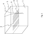
- Fig. 2 also shows the treated solid body 1, wherein on at least one surface of the solid body 1, in particular partially or completely covering or overlying the surface 5, a receiving layer 140 for introducing stresses into the solid body 1 is arranged, in particular attached or generated.
- the receiving layer 140 preferably consists of a polymer material or comprises a polymer material, in particular PDMS.
- the receiving layer 140 contracts and thereby introduces stresses into the solid body 1, through which a crack triggered and/or generated and/or guided to separate the solid portion from solid 1.
- At least individual, several or the majority of the regions in which the modification blocks 91, 92 are generated are many times larger, in particular at least 1.1 times or 1.5 times or 1.8 times or 2 times or 2.5 times or 3 times or 4 times, than the regions in which no modifications 9 or fewer modifications 9 are generated.
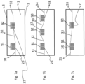
- the Figures 6a-6c show a further embodiment of the present invention.
- the modification blocks 91, 92 serve to generate local material weakenings or local solid cracks or local stress increases.
- Reference numeral 25 denotes a first partial detachment region or crack portion in which the local material weakenings or local Solid-state cracks or local stress increases occur
- the reference numeral 27 designates a second partial detachment region or crack portion in which the local material weakening or local solid-state cracks or local stress increases also occur.
- the individual partial detachment regions or crack portions preferably form ends 71, 72, beyond which the respective partial detachment region or crack portion can be enlarged.
- the enlargement of the partial detachment regions or crack portions preferably occurs as a result of a by means of the receiving layer 140 (cf. Fig. 2 ) caused force introduction.
- the detachment region 2 is formed by the following components: crack 31 between the outer edge and the first modification block 91, followed by the first crack portion 25, which is directly generated by the first block 91 at modifications 9, followed by crack 32 between the two modification blocks 91 and 92, followed by the second crack portion 27, which is directly generated by the second block 92 at modifications 9, followed by the crack 33 between the modification block 92 and the further outer edge of the solid body 1. It is thereby apparent that the detachment region 2 can be predetermined in such a way that a crack for separating the solid layer 12 from the solid body 1 can run in sections on different levels.
- the detachment area 2 can be selected such that the crack path contains several geometric turning points.
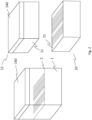
- FIGs 8a-8c show a multiple processing of a solid body 1, in particular an ingot, wherein the solid body 1 is thinned by a solid portion 12, in particular a solid layer 12.
- a receiving layer 140 for receiving the solid portion 12 and for initiating and/or supporting a crack can also be arranged on the surface 5, 502, 504.
- the Figures 8a-8c thus each show the exposure of the solid body 1 to LASER radiation from the LASER light source, wherein the laser beams penetrate into the solid body 1 via a surface 5, 502, 504 of the solid body layer 12 to be separated.
- LASER radiation a predetermined portion of the solid body 1 inside the solid body 1 is tempered in a defined manner to form a detachment region 2 or several partial detachment regions.
- the temperature generated in the predetermined portion of the solid body 1 is preferably so high that the material forming the predetermined portion undergoes modification 9 in the form of a predetermined material transformation.
- the number and arrangement of the modifications 9 is adjustable and is preferably predetermined.
- the residual solid body 1 is again exposed to laser radiation from the laser light source, whereby the laser radiation heats a predetermined portion of the residual solid body 1 inside the residual solid body 1 to form a detachment region 2, and the temperature generated in the predetermined portion of the residual solid body 1 is again sufficiently high that the material forming the predetermined portion undergoes a predetermined material transformation.
- solid portions 12 of the same, similar, or different thicknesses, in particular solid layers 12, in particular wafers can be separated from a solid body 1.
- the solid body 1 has a length such that a plurality, in particular more than 2 or more than 5 or more than 10 or more than 20 or more than 50 or more than 100 or more than 150 or more than 200, solid body layers 12 with a thickness of less than 1000 ⁇ m, in particular less than 800 ⁇ m or less than 500 ⁇ m or less than 300 ⁇ m or less than 200 ⁇ m or less than 150 ⁇ m or less than 110 ⁇ m or less than 75 ⁇ m or less than 50 ⁇ m, can be separated therefrom.
- the newly exposed surface 502, 504 of the remaining solid body 1 is machined.
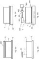
- Fig. 9a shows the provision of the solid 1, in particular an ingot.
- the provided solid body 1 is arranged on a cooling device 3.
- the cooling device 3 is preferably a cooling chuck.
- the solid body 1 is particularly preferably coupled or glued or welded or screwed or clamped to a tool carrier (chuck), wherein the tool carrier preferably comprises a cooling functionality and thereby preferably becomes the cooling device 3.
- the tool carrier preferably consists of an alloy with a composition of 45%-60%, in particular 54%, iron, 20%-40%, in particular 29% nickel and 10%-30%, in particular 17% cobalt. The percentages refer to the proportion of the total mass.
- An example of a preferred cooling device 3 is shown in Fig. 11 shown.
- the solid body 1 and the cooling device 3 preferably have the same or a similar thermal expansion.
- Similar thermal expansion is preferably understood here as any thermal expansion with a temperature increase of 10°C in a temperature range from -200°C to 200°C, in which the difference between the thermal expansions of the solid body 1 and the cooling device 3 is less than 50%, in particular less than 25% or less than 10%, of the thermal expansion of the object expanding the most (cooling device or ingot).
- the thermal expansion of the solid body 1 is preferably less than 10 ppm/K, in particular less than 8 ppm/K or less than 5 ppm/K, such as less than 4 ppm/K or substantially 4 ppm/K or exactly 4 ppm/K.
- the solid body 1 is preferably fixed, in particular glued, to the cooling device 3 in the longitudinal direction with its underside 7, which is preferably located longitudinally opposite the surface 5.
- the laser beams are introduced into the solid body 1 in the direction of the cooling device 3 via the surface 5, which is part of the solid layer 12 to be separated.
- Fig. 9c shows schematically the generation of the modifications 9 by means of the laser beams.
- the cooling device 3 ensures that the energy or heat introduced into the solid body 1 by the laser beams is at least partially, and preferably mostly, dissipated from the solid body 1.
- Fig. 9d shows a schematic sectional view of the solid body 1 after the creation of the modifications 9.
- four blocks of modifications 9 can be seen, which lead to the four crack portions 25, 27, 28, 29.
- Fig. 9e shows a state in which a receiving layer 140, in particular comprising a polymer material, is arranged or produced on the surface 5 through which the laser beams penetrated the solid body 1.
- the receiving layer 140 is preferably produced as a film and, after its production, is adhered to the surface 5.
- Fig. 9f schematically shows a temperature control of the receiving layer 140.
- the receiving layer 140 is tempered, in particular cooled, to a temperature below the ambient temperature, in particular to a temperature of less than 20°C, or less than 1°C, or less than 0°C, or less than -10°C, or less than -50°C, or less than -100°C.
- the material of the receiving layer 140 undergoes a glass transition as a result of the cooling.
- the temperature control of the receiving layer 140 is carried out using liquid nitrogen. Due to the temperature control, in particular due to the glass transition, the receiving layer 140 contracts, thereby generating mechanical stresses in the solid body 1. Due to the mechanical stresses, a crack connecting the crack portions 25, 27, 28, 29 is triggered, through which the solid body portion 12 is separated from the solid body 1.
- Fig. 10a shows a representation according to the Fig. 9f shown tempering of the receiving layer 140.
- the solid body portion 12 is separated from the solid body 1 with the receiving layer 140 still arranged thereon.
- Fig. 10b shows a further step of introducing modifications 9 into the residual solid body 1, which is reduced in length at least by the already separated solid layer 12.
- Fig. 10c schematically shows a further preferred embodiment.
- the cooling device 3 is coupled, on the one hand, to the solid body 1 and, on the other hand, to a displacement device 30, in particular an X/Y displacement device or a rotary table.
- the displacement device 30 causes a movement of the solid body 1, whereby it can be moved in a defined manner relative to the environment and a laser optics system, in particular a scanner.
- Fig. 10d shows a more detailed schematic representation of the Fig. 10c
- the round arrow within the displacement device 30 indicates that it is rotatable.
- a coupling layer in particular an adhesive layer, is provided between the solid body 1 and the cooling device 3.
- the coupling layer 30 is preferably designed such that it can withstand a plurality of processing cycles, in particular more than 200 or more than 300 or more than 500 processing cycles, under high mechanical and thermal stress.
- the laser beam source 401 preferably guides laser beams along a first laser beam guide 402 to an optics 40, from where the laser beams reach a scanner via a further laser beam guide 403.
- at least the laser beam source 401 and the scanner 400 are provided.
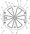
- Fig. 11 shows the cooling device 3.
- the cooling device 3 preferably has a guide-support structure, which is preferably formed by a tool carrier, in particular a chuck.
- the guide-support structure preferably has a round basic shape. This is advantageous because imbalance can be more easily avoided with regard to spinning processes.
- the round basic shape is preferably provided with flattened portions 95-98. These flattened portions are advantageous because they allow or facilitate rough alignment and/or cassette assembly.
- the cooling device 3, in particular the guide-support structure of the cooling device 3, has good thermal conductivity.
- the cooling device 3 is preferably made of anodized aluminum, which reduces or prevents abrasion particles. This is advantageous because it increases cleanroom compatibility.
- the chuck is preferably compatible with the detachment process.
- the alignment elements 65-68 are preferably provided.
- the alignment elements 65-68 are preferably designed as alignment holes, slots, or pins.
- the alignment elements 65-68 preferably form drivers for the non-positive and/or positive rotation transmission.
- the alignment elements 65-68 preferably have steel or ceramic inserts, thereby achieving high wear resistance.
- the alignment elements 65-68 preferably serve to couple the cooling device 3 to the displacement device 30.
- dowel pins can be provided, which can be designed, for example, as hold-down devices, whereby, for example, a force and/or form fit with the guide-support structure can be generated.
- a notch, groove, or marking 76 is preferably provided on the cooling device 3. This feature is advantageous because it allows the solid orientation, in particular the ingot orientation, to be identified. Knowledge of the orientation of the solid, in particular the ingot, can be utilized to adapt the modifications 9 produced by the laser beams to the crystallographic orientation.
- Reference numeral 75 denotes, purely by way of example, an optional data carrier element and/or data transmission element and/or data acquisition element.
- the element denoted by reference numeral 75 is preferably embodied as a barcode and/or RFID element and/or SAW sensor. This particularly allows for integration into a Manufacturing Execution System (MES).
- MES Manufacturing Execution System
- cooling channels for conducting a cooling fluid are preferably provided or formed on or in the guide-support structure.
- the cooling channel(s) 78 can serve to control the temperature of the solid body 1, the cooling device 3, and/or a machine mount, in particular the displacement device 30.
- Cooling fluid in particular a liquid, can be fed into the cooling channel 78 via an inlet 77 and removed via an outlet 79.
- the interface or the coupling layer between the solid body 1 and the cooling device 3 preferably has a high thermal conductivity, in particular corresponding to the thermal conductivity of the solid body 1 or the cooling device 3.
- the cooling device 3 can additionally or alternatively be cooled via the air interface. At high rotational speeds or displacement speeds of the displacement device 30, the air layer forming around the cooling device 3 is very thin, whereby heat can be dissipated very well.
- active thermostatting is preferably integrated into the MES. Additionally or alternatively, process monitoring for different substrate sizes and thicknesses is provided.
- the fluid channels are preferably sealed by pressing when mounted in a fixed position and by means of a central ring seal when rotating.
- Reference numeral 69 denotes an optional sensor device, which is preferably designed as a temperature sensor.
- the sensor device is preferably a SAW temperature sensor.
- the method according to the invention preferably also comprises the step of providing an optics 40, 608, wherein the optics 608 preferably has at least two deflection elements 610, 612 for deflecting light beam components 616, 618.
- the light beams 616, 618 are preferably generated and emitted by the laser beam source 401.
- the method according to the invention preferably comprises the step of deflecting at least two mutually different light beam components 616, 618 of the emitted light beam 606 by means of the deflection elements 610, 612, 613, wherein the light beam components 616, 618 are deflected such that they penetrate the solid body 1.
- the method according to the invention preferably comprises the step of deflecting the light beams 606 by means of the deflection elements 610, 612, 613, wherein the light beams 606 are deflected such that they penetrate into the solid body 1 and wherein the mutually different deflected light beams 606 meet in a focus 620 within the solid body 1 and the physical modification 9, in particular in the form of a lattice defect, is generated by the light beams meeting in the focus 620 (6) is generated.
- At least two mutually different light beam components 616, 618 of at least one emitted light beam 606, in particular the light beam components of a plurality of emitted light beams, or the plurality of emitted light beams 606 are deflected by means of the deflection elements 610, 612, 613, wherein the light beam components 616, 618 or the light beams 606 are deflected in such a way that they penetrate into the solid body 1 and wherein the mutually different deflected light beam components 616, 618 or the mutually different deflected light beams 606 meet in a focus 620 within the solid body 1 and the physical modification 9, in particular in the form of a lattice defect, is generated by the light beam components 616, 618 or light beams 606 meeting in the focus 620.
- At least two light beams 606 and preferably all light beams 606 can be divided into light beam components 616, 618 which are different from one another, in particular travel different paths, and penetrate into the solid body 1 at spaced-apart surface components 622, 624 of the solid body 1, wherein the light beam components 616, 618 of a respective light beam are deflected by means of deflection elements 610, 612, 613 which are different from one another.
- the optics 608 preferably has at least one light beam splitting means 633, in particular a half mirror or beam splitter, and at least one light beam 606 is split into at least two light beam components 616, 618 by means of at least the light beam splitting means 633.
- a light beam 606 is split into at least two light beam components 616, 618 by means of a light beam splitting means 633, in particular a half mirror, wherein a light beam component 616 is deflected by means of at least two deflection elements 610, 612, 613, in particular mirrors, is deflected such that it coincides with the other light beam portion 618 in the interior of the solid body 1 to form a focus 620 for generating the physical modification 9.
- a plurality of physical modifications 9 are generated, wherein the physical modifications 9 preferably form or describe a plane and/or a contour and/or a silhouette and/or the external shape of a body.
- the at least one light beam 606 emitted by the laser beam source 401 preferably consists of coherent light, and the light waves of the light beam components 616, 618 converging at the focus 620 preferably have the same phase and the same frequency.
- At least one light beam portion 616, 618 or at least one light beam 606 is deflected and focused by a deflection element 610, 612, 613 designed as a parabolic mirror.
- the at least one light beam portion 616, 618 or the at least one light beam 606 preferably passes through a deflection element 610, 612, 613, in particular the parabolic mirror, a beam shaping device, in particular a 1D telescope, for changing the focus shape before deflection and focusing.
- the laser beam source 401 preferably generates at least or exactly two light beams, wherein the light beams 606 are generated with different colors depending on the band gap of the material of the solid body 1 such that the modification 9 is generated by a two-photon process.
- a first laser field is formed by a first light beam 606, wherein the first light beam 606 comprises photons with a first energy
- a second laser field is preferably formed by a second light beam 606, wherein the second laser beam 606 comprises photons with a second energy, wherein the first laser field is weaker than the second laser field and the first energy is greater than the second energy.
- Fig. 13 shows the creation of modifications using two laser beams or two laser beam components in a schematic representation.
- the modifications 9 preferably have a vertical dimension of less than 50 ⁇ m, preferably less than 30 ⁇ m, and particularly preferably less than 20 ⁇ m.
- the focus 620 is preferably less than 1000 ⁇ m and preferably less than 500 ⁇ m and more preferably less than 200 ⁇ m from a penetration surface 626 of the solid 1, wherein at least individual light beam components 616, 618 penetrate into the solid body 1 via the penetration surface 626 to produce the physical modification 9.
- the focus 620 is preferably generated in an overlapping portion of at least two intersecting light beam waists 630, 632, wherein the light beam waists 630, 632 are generated by the light beam portions 616, 618 or light beams 606.
- Fig. 14a to 14c show different microscopic representations of a solid body 1 conditioned or modified by means of a laser, in particular predominantly or substantially or completely consisting of, for example, a semiconductor material, in particular of SiC.
- FIG. 14a A 6H-SiC line defect field 1E is shown, which was generated with pulse spacings of 0.4 ⁇ m, line spacings of line-generated crystal lattice modifications 20, 22 of 2 ⁇ m, and a pulse repetition frequency of 128 kHz.
- the pulse spacings can be set between 0.01 ⁇ m and 10 ⁇ m and/or the line spacings can be set between 0.01 ⁇ m and 20 ⁇ m and/or the pulse repetition frequency can be set between 16 kHz and 1024 kHz.
- Fig. 14b is an enlarged detail of the frame in Fig. 14a marked area. It can be seen that the block spacings 24, 26 are preferably uniform and amount to, for example, 66 ⁇ m. Fig. 14c also shows block spacings of approximately 66 ⁇ m. However, it is also conceivable that the block spacings lie in other ranges, such as between 4 ⁇ m and 1000 ⁇ m.
- the representation of the Fig. 14a represents a plan view of a solid through a polished surface of the solid.
- the structure shown is thus formed within the solid or has been created by modification, in particular by means of a laser.
- FIG. 15a show microscopic representations of solids modified according to the invention.
- Reference numeral 14 preferably designates the location of a processing start, ie the location at which the modification of the crystal lattice of the solid body 1 is preferably started.
- Reference numeral 9 designates the modified region in the solid body 1. It is evident from this illustration that off-center of the modified region 9 or offset from the center 15 of the modified region 9, a crack 13 propagates in the solid body 1. It is possible here for the location and direction of propagation of the crack 13 to be predetermined by defined parameters for generating the modification, with the crack 13 in the example shown preferably running parallel or substantially parallel to the main surface 18. The crack 13 can thus be specifically generated, triggered, and guided through the modifications 9, at the edge of the modifications 9, or at a distance from the modifications 9, by setting the parameters.
- the underside of the solid body 1, in particular of the wafer, is indicated by reference numeral 7.
- reference numeral 17 indicates a reference length, which preferably measures 50 ⁇ m.
- the cross-sectional area shown extends perpendicular to the main surface 18 of the solid body 1, i.e., over the height of the lateral surface 19, wherein the modifications 9 are preferably introduced into the solid body 1 via the main surface 18, or the generation of the modifications 9 is preferably effected through the main surface 18.
- the main surface 18 is particularly preferably many times larger than the lateral surface 19, in particular at least twice, at least three times, at least four times, at least 10 times, at least 20 times, or at least 50 times.
- Fig. 15a preferably shows a 6H-SiC line defect field 1C, which was generated with pulse spacings of 0.2 ⁇ m, line spacings of line-generated crystal lattice modifications 20, 22 of 3 ⁇ m, and a pulse repetition frequency of 128 kHz.
- the pulse spacings can be provided between 0.01 ⁇ m and 10 ⁇ m and/or the line spacings can be provided between 0.01 ⁇ m and 20 ⁇ m and/or the pulse repetition frequency can be provided between 16 kHz and 1024 kHz.
- Fig. 15b shows a plan view of a part of the solid body 1 and through the polished main surface 18 onto the modifications 9.
- the individual modifications 9 are produced in such a way that several of them form a line 20, 22.
- the modifications are produced homogeneously, at least partially, in more than one direction, in particular in two directions, in at least two directions, or in three directions.
- the modifications 9 are particularly preferably produced uniformly or homogeneously distributed in a plane parallel to the main surface 18.
- in one direction length or width or height
- the modifications 9 are created in such a way that they represent patterns.
- the modifications 9 within the meaning of the present invention can be created in different regions of the solid body 1, wherein the regions preferably have the same dimensions, in different numbers and/or with different parameters.
- the reference number 17 indicates Fig. 14b a reference length, preferably measuring 100 ⁇ m.
- Fig. 16a preferably shows a 6H-SiC line defect field 1A, which was generated with pulse spacings of 0.2 ⁇ m, line spacings of line-generated crystal lattice modifications 20, 22 of 1 ⁇ m and a pulse repetition frequency of 128 kHz.
- the pulse spacings can be provided between 0.01 ⁇ m and 10 ⁇ m and/or the line spacings can be provided between 0.01 ⁇ m and 20 ⁇ m and/or the pulse repetition frequency can be provided between 16 kHz and 1024 kHz.
- a crack 13 propagates in the solid body 1 at a distance from the generated modifications 9.
- the crack 13 thus propagates at a distance from the center of the modifications 9, or the crack propagates in a region of the solid body 1 that is at a distance from the main modification portion.
- the main modification portion is, for example, in the case of modifications 9 generated by a laser, preferably the portion of the solid body 1 in which the laser has its focus.
- the reference number 17 denotes a reference length, which is preferably 100 ⁇ m.
- Figures 17a to 176f show different representations of the modification-crack generation relationship.
- Fig. 6a shows, for example, a modification 9 shaped according to the shape of a laser waist.
- the shape of the modification 9 is only shown schematically.
- a modification 9 can preferably have a shape that lies in the design space between a spherical shape, in particular a circle, and a polygon, in particular a quadrilateral, in particular a rectangle, such as a square.
- the Fig. 6a that the detachment region 2 does not extend through the center Z of the modification 9.
- the Detachment area 2 spaced by 1/20 or 1/10 or 1/5 or 1/4 or 1/3 or half of the maximum length of modification 9 from the center of the modification.
- Fig. 17b shows, for example, a variant according to which the detachment region 2 runs past the modification 9 at the outer edge or in the region of the outer edge of the modification 9 and the modification therefore particularly preferably only passes outside but does not run through the modification.
- Fig. 17c shows a further variant according to which the detachment region 2 is preferably spaced from the modification 9 by at least 0.01 ⁇ m or by at least 0.1 ⁇ m or by at least 1 ⁇ m or by at least 5 ⁇ m or by at least 10 ⁇ m.
- Figures 6d to 6f are analogous to the Figures 17a to 17c built.
- the Figures 17d to 17e show a variant according to which the effect achieved by modification 9, namely the local severing of the crystal lattice of the solid 1, only arises through the interaction of several modifications 9, in particular of at least 2, 5, 10, 20, 50 or at least 100 modifications.
- the Figures 18a to 18d show various arrangements of modifications 9 and the detachment areas 2 resulting from the modification 9.
- the parameters required to generate the modification can therefore be set in such a way that the detachment area 2 runs through the modifications 9 (cf. Fig. 18a and 18b ) or that the detachment area is spaced from the modifications 9. (cf. Fig. 18c-18d ).
- FIGS 19a-19d show further variants according to which a detachment region 2 is formed as a result of the generation of modifications 9 in a solid body 1.
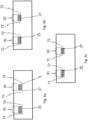
- the centers of the modifications 9 and 23 can be provided on one side of the detachment region 2.
- the modifications are generated identically except for the location of their generation (in particular the distance to the main surface).
- the focus and/or the amount of energy and/or the exposure time, etc. change.
- Figures 19c to 19d the centers of modifications 9 and 23 are each on different sides of the detachment area 2.
- the centers of the modifications 9, 23 are formed at the same distance or at different distances from the detachment region 2. Furthermore, it is conceivable that, in addition to or as an alternative to the location of the modifications 9, 23, the focus and/or the amount of energy and/or the exposure time, etc., change or are set differently.
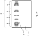
- Fig. 20 shows an arrangement according to which the modifications 9 are generated locally in different concentrations (AD) and/or distributions.
- AD concentrations
- Fig. 20 shows an arrangement according to which the modifications 9 are generated locally in different concentrations (AD) and/or distributions.
- AD concentrations
- Fig. 20 shows an arrangement according to which the modifications 9 are generated locally in different concentrations (AD) and/or distributions.
- AD concentrations
- Fig. 20 shows an arrangement according to which the modifications 9 are generated locally in different concentrations (AD) and/or distributions.
- AD concentrations
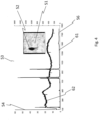
- Fig. 21 shows a top view of a 6H-SiC line defect parameter field 1C, preferably with a laser damage area of 1 cm2 and a thickness of 245 ⁇ 3 ⁇ m.
- the top view is taken through the polished main surface of the solid body 1 and shows a state before the separation of a solid body layer 11 along the detachment region 2.
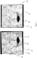
- Fig. 22a and 22b preferably show two views of a 6H-SiC line defect parameter field 1C, wherein a laser damage of 1 cm 2 and a thickness of 120 +/-3 ⁇ m is preferably present.
- the two surface structures shown were created by the separation of the solid body 1 into two parts.
- the reference numeral 60 denotes cracks extending in or substantially in the horizontal direction.
- the Fig. 22a In addition to the cracks 60 also laser damage.
- Fig. 22b shown surface is opposite to that in Fig. 22a The surface shown is significantly more homogeneous and exhibits fewer damages and/or cracks.
- Reference numeral 17 denotes a reference length, which is preferably 1000 ⁇ m.
- Fig. 23 shows schematically that the crystal lattice of the solid body 1 is altered by the introduction or generation of modifications 9 in such a way that crack-guiding stresses 50 are generated, preferably at a distance from the center Z of the modification(s) 9.
- crack-guiding stresses 50 are generated in the crystal lattice by the modifications 9 in at least one solid body region surrounding a modification 9 in such a way that a crack separating the solid body 1 is guided by the crack-guiding stresses 50, in particular offset from the center Z of the respective modifications 9.
- the oval-shaped crack guiding stresses 50 define, according to the invention, a detachment area 2 along and through which a crack caused by mechanical Tensions generated crack is guided.
- the mechanical stresses are preferably generated or introduced into the solid body 1 via the tempering of a layer arranged or generated on the solid body 1.
- the present invention can relate to a method for separating at least one solid portion from a solid, in particular a wafer.
- the method comprises at least the following steps: modifying the crystal lattice of the solid using a laser, in particular a picosecond or femtosecond laser, wherein a plurality of modifications are generated in the crystal lattice, wherein the crystal lattice cracks at least in one portion each in the regions surrounding the modifications as a result of the modifications, wherein the cracks in the region of the modifications define one or more partial detachment regions.
- the method can comprise the step of providing a solid 1 to be processed, wherein the solid 1 preferably consists of a chemical compound.
- a LASER light source can be provided, in particular as a modification device.
- the solid body 1 is preferably additionally exposed to LASER radiation from the LASER light source, wherein the LASER radiation heats a predetermined portion of the solid body 1 inside the solid body 1 in a defined manner to form a detachment region (2), wherein the temperature generated in the predetermined portion of the solid body 1 is so high that the material forming the predetermined portion undergoes a predetermined material transformation.
- the detachment of the solid layer from the solid body can thus result solely from the modifications produced according to the invention.
- a receiving layer on the solid body to hold the solid body portion and then to subject the receiving layer to thermal stress to generate, in particular mechanical, stresses in the solid body, whereby the stresses a crack, in particular a main crack, in which the solid propagates along the detachment region through which the solid layer is separated from the solid, preferably at least the majority of the partial cracks possibly previously generated in the region of the modifications are connected to one another by the crack.
- a method for creating a detachment region in a solid body for detaching a solid portion, in particular a solid layer, from the solid body is described, wherein the solid portion to be detached is thinner than the solid body reduced by the solid portion, at least comprising the steps of: providing a solid body to be processed, wherein the solid body preferably consists of a chemical compound; providing a laser light source; Exposure to the solid body with LASER beams from the LASER light source, wherein the laser beams penetrate into the solid body via a surface of the solid body portion to be separated, wherein the LASER beams apply a defined action to a predetermined portion of the solid body inside the solid body to form a detachment region or a plurality of partial detachment regions, characterized in that the laser exposure successively produces a plurality of modifications in the crystal lattice of the solid body, wherein the crystal lattice cracks as a result of the modifications in the regions surrounding the modifications, at least in a portion thereof, wherein the crack
- a method for separating at least one solid portion from a solid, in particular a wafer is described, at least comprising the steps of: modifying the crystal lattice of the solid by means of a modifying agent, in particular a laser, in particular a picosecond or femtosecond laser, wherein a plurality of modifications are generated in the crystal lattice, wherein the crystal lattice tears as a result of the modifications in the regions surrounding the modifications, at least in a respective portion thereof, wherein a detachment region is defined by the cracks in the region of the modifications, arranging a receiving layer on the solid for holding the solid portion, thermally loading the receiving layer for, in particular mechanically, generating stresses in the solid, wherein the stresses cause a main crack in the solid to propagate along the detachment region, which connects at least the majority of the cracks in the region of the modifications to one another.
- a modifying agent in particular a laser, in particular a picosecond or femtosecond laser
Landscapes
- Engineering & Computer Science (AREA)
- Physics & Mathematics (AREA)
- Optics & Photonics (AREA)
- Mechanical Engineering (AREA)
- Plasma & Fusion (AREA)
- General Chemical & Material Sciences (AREA)
- Chemical Kinetics & Catalysis (AREA)
- Chemical & Material Sciences (AREA)
- Power Engineering (AREA)
- Microelectronics & Electronic Packaging (AREA)
- Computer Hardware Design (AREA)
- Manufacturing & Machinery (AREA)
- General Physics & Mathematics (AREA)
- Condensed Matter Physics & Semiconductors (AREA)
- Oil, Petroleum & Natural Gas (AREA)
- Laser Beam Processing (AREA)
- Mechanical Treatment Of Semiconductor (AREA)
- Processing Of Stones Or Stones Resemblance Materials (AREA)
- Crystals, And After-Treatments Of Crystals (AREA)
- Dicing (AREA)
- Physical Or Chemical Processes And Apparatus (AREA)
Priority Applications (1)
| Application Number | Priority Date | Filing Date | Title |
|---|---|---|---|
| EP25158308.4A EP4530010A3 (de) | 2014-11-27 | 2015-11-27 | Festkörperteilung mittels stoffumwandlung |
Applications Claiming Priority (8)
| Application Number | Priority Date | Filing Date | Title |
|---|---|---|---|
| DE102014017583 | 2014-11-27 | ||
| DE102014017582 | 2014-11-27 | ||
| DE102014018841.8A DE102014018841A1 (de) | 2014-11-27 | 2014-12-17 | Laserbasiertes Trennverfahren |
| DE102014018720.9A DE102014018720A1 (de) | 2014-11-27 | 2014-12-17 | Festkörpertrennverfahren mit laserbasierter Vorschädigung |
| DE102015000449.2A DE102015000449A1 (de) | 2015-01-15 | 2015-01-15 | Festkörperteilung mittels Stoffumwandlung |
| EP15801449.8A EP3223993A2 (de) | 2014-11-27 | 2015-11-27 | Festkörperteilung mittels stoffumwandlung |
| EP20151833.9A EP3666445B1 (de) | 2014-11-27 | 2015-11-27 | Festkörperteilung mittels stoffumwandlung |
| PCT/EP2015/077981 WO2016083610A2 (de) | 2014-11-27 | 2015-11-27 | Festkörperteilung mittels stoffumwandlung |
Related Parent Applications (3)
| Application Number | Title | Priority Date | Filing Date |
|---|---|---|---|
| EP15801449.8A Division EP3223993A2 (de) | 2014-11-27 | 2015-11-27 | Festkörperteilung mittels stoffumwandlung |
| EP20151833.9A Division EP3666445B1 (de) | 2014-11-27 | 2015-11-27 | Festkörperteilung mittels stoffumwandlung |
| EP20151833.9A Division-Into EP3666445B1 (de) | 2014-11-27 | 2015-11-27 | Festkörperteilung mittels stoffumwandlung |
Related Child Applications (1)
| Application Number | Title | Priority Date | Filing Date |
|---|---|---|---|
| EP25158308.4A Division EP4530010A3 (de) | 2014-11-27 | 2015-11-27 | Festkörperteilung mittels stoffumwandlung |
Publications (2)
| Publication Number | Publication Date |
|---|---|
| EP4122633A1 EP4122633A1 (de) | 2023-01-25 |
| EP4122633B1 true EP4122633B1 (de) | 2025-03-19 |
Family
ID=56075088
Family Applications (6)
| Application Number | Title | Priority Date | Filing Date |
|---|---|---|---|
| EP22195120.5A Active EP4122633B1 (de) | 2014-11-27 | 2015-11-27 | Festkörperteilung mittels stoffumwandlung |
| EP15801449.8A Withdrawn EP3223993A2 (de) | 2014-11-27 | 2015-11-27 | Festkörperteilung mittels stoffumwandlung |
| EP25158308.4A Pending EP4530010A3 (de) | 2014-11-27 | 2015-11-27 | Festkörperteilung mittels stoffumwandlung |
| EP20151833.9A Active EP3666445B1 (de) | 2014-11-27 | 2015-11-27 | Festkörperteilung mittels stoffumwandlung |
| EP18175761.8A Active EP3395489B1 (de) | 2014-11-27 | 2015-11-27 | Festkörperteilung mittels stoffumwandlung |
| EP18178276.4A Active EP3399542B1 (de) | 2014-11-27 | 2015-11-27 | Festkörperteilung mittels stoffumwandlung |
Family Applications After (5)
| Application Number | Title | Priority Date | Filing Date |
|---|---|---|---|
| EP15801449.8A Withdrawn EP3223993A2 (de) | 2014-11-27 | 2015-11-27 | Festkörperteilung mittels stoffumwandlung |
| EP25158308.4A Pending EP4530010A3 (de) | 2014-11-27 | 2015-11-27 | Festkörperteilung mittels stoffumwandlung |
| EP20151833.9A Active EP3666445B1 (de) | 2014-11-27 | 2015-11-27 | Festkörperteilung mittels stoffumwandlung |
| EP18175761.8A Active EP3395489B1 (de) | 2014-11-27 | 2015-11-27 | Festkörperteilung mittels stoffumwandlung |
| EP18178276.4A Active EP3399542B1 (de) | 2014-11-27 | 2015-11-27 | Festkörperteilung mittels stoffumwandlung |
Country Status (8)
Families Citing this family (41)
| Publication number | Priority date | Publication date | Assignee | Title |
|---|---|---|---|---|
| DE102015000449A1 (de) | 2015-01-15 | 2016-07-21 | Siltectra Gmbh | Festkörperteilung mittels Stoffumwandlung |
| EP4122633B1 (de) | 2014-11-27 | 2025-03-19 | Siltectra GmbH | Festkörperteilung mittels stoffumwandlung |
| WO2016083609A2 (de) | 2014-11-27 | 2016-06-02 | Siltectra Gmbh | Laserbasiertes trennverfahren |
| JP6698468B2 (ja) * | 2016-08-10 | 2020-05-27 | 株式会社ディスコ | ウエーハ生成方法 |
| DE102017010284A1 (de) * | 2017-11-07 | 2019-05-09 | Siltectra Gmbh | Verfahren zum Dünnen von mit Bauteilen versehenen Festkörperschichten |
| KR102775360B1 (ko) | 2017-04-20 | 2025-03-05 | 실텍트라 게엠베하 | 구성 요소가 제공된 고상 층의 두께를 감소시키는 방법 |
| DE102017003830A1 (de) | 2017-04-20 | 2018-10-25 | Siltectra Gmbh | Verfahren zur Waferherstellung mit definiert ausgerichteten Modifikationslinien |
| DE102017007585A1 (de) | 2017-08-11 | 2019-02-14 | Siltectra Gmbh | Vorrichtung und Verfahren zum Beaufschlagen von Spannungserzeugungsschichten mit Druck zum verbesserten Führen eines Abtrennrisses |
| JP6923877B2 (ja) * | 2017-04-26 | 2021-08-25 | 国立大学法人埼玉大学 | 基板製造方法 |
| DE102017007586A1 (de) | 2017-08-11 | 2019-02-14 | Siltectra Gmbh | Fertigungsanlage zum Abtrennen von Wafern von Spendersubstraten |
| MY207820A (en) * | 2017-09-04 | 2025-03-20 | Lintec Corp | Thinned plate member production method and thinned plate member production device |
| JP6943388B2 (ja) * | 2017-10-06 | 2021-09-29 | 国立大学法人埼玉大学 | 基板製造方法 |
| CN107731887B (zh) * | 2017-11-22 | 2020-05-19 | 武汉华星光电半导体显示技术有限公司 | 柔性oled显示面板的制备方法 |
| DE102018001327A1 (de) * | 2018-02-20 | 2019-08-22 | Siltectra Gmbh | Verfahren zum Erzeugen von kurzen unterkritischen Rissen in Festkörpern |
| JP7256604B2 (ja) * | 2018-03-16 | 2023-04-12 | 株式会社ディスコ | 非破壊検出方法 |
| US10940611B2 (en) | 2018-07-26 | 2021-03-09 | Halo Industries, Inc. | Incident radiation induced subsurface damage for controlled crack propagation in material cleavage |
| US11309191B2 (en) | 2018-08-07 | 2022-04-19 | Siltectra Gmbh | Method for modifying substrates based on crystal lattice dislocation density |
| JP7327920B2 (ja) * | 2018-09-28 | 2023-08-16 | 株式会社ディスコ | ダイヤモンド基板生成方法 |
| CN113056346B (zh) | 2018-10-30 | 2023-12-15 | 浜松光子学株式会社 | 激光加工装置及激光加工方法 |
| JP7120904B2 (ja) | 2018-10-30 | 2022-08-17 | 浜松ホトニクス株式会社 | レーザ加工装置及びレーザ加工方法 |
| WO2020090894A1 (ja) | 2018-10-30 | 2020-05-07 | 浜松ホトニクス株式会社 | レーザ加工装置及びレーザ加工方法 |
| JP7246919B2 (ja) * | 2018-12-21 | 2023-03-28 | 浜松ホトニクス株式会社 | レーザ加工方法、半導体部材製造方法及びレーザ加工装置 |
| US11024501B2 (en) | 2018-12-29 | 2021-06-01 | Cree, Inc. | Carrier-assisted method for parting crystalline material along laser damage region |
| US10562130B1 (en) * | 2018-12-29 | 2020-02-18 | Cree, Inc. | Laser-assisted method for parting crystalline material |
| US10576585B1 (en) * | 2018-12-29 | 2020-03-03 | Cree, Inc. | Laser-assisted method for parting crystalline material |
| DE102019201438B4 (de) * | 2019-02-05 | 2024-05-02 | Disco Corporation | Verfahren zum Herstellen eines Substrats und System zum Herstellen eines Substrats |
| JP7178491B2 (ja) * | 2019-04-19 | 2022-11-25 | 東京エレクトロン株式会社 | 処理装置及び処理方法 |
| DE102019111985A1 (de) | 2019-05-08 | 2020-11-12 | Infineon Technologies Ag | Verfahren zum herstellen von siliziumcarbid-vorrichtungen und wafer-verbund, der mit laser modifizierte zonen in einem handhabungssubstrat enthält |
| US10611052B1 (en) | 2019-05-17 | 2020-04-07 | Cree, Inc. | Silicon carbide wafers with relaxed positive bow and related methods |
| SE1950611A1 (en) | 2019-05-23 | 2020-09-29 | Ascatron Ab | Crystal efficient SiC device wafer production |
| US12098476B2 (en) | 2019-08-06 | 2024-09-24 | Kwansei Gakuin Educational Foundation | Method for producing a SiC substrate via an etching step, growth step, and peeling step |
| DE102019122614B4 (de) | 2019-08-22 | 2025-05-15 | Infineon Technologies Ag | Ausgangssubstrat, wafer-verbund und verfahren zum herstellen von kristallinen substraten und halbleitervorrichtungen |
| US20220375749A1 (en) | 2019-09-27 | 2022-11-24 | Kwansei Gakuin Educational Foundation | Method of manufacturing sic semiconductor device and sic semiconductor device |
| WO2021060365A1 (ja) | 2019-09-27 | 2021-04-01 | 学校法人関西学院 | 半導体基板の製造方法及び半導体基板の製造装置 |
| EP3984687A1 (de) * | 2020-10-16 | 2022-04-20 | Bystronic Laser AG | Strahlbearbeitungskopf und verfahren zur strahlbearbeitung |
| JP7706126B2 (ja) * | 2021-10-07 | 2025-07-11 | 株式会社デンソー | ウエハの製造方法 |
| EP4163046A1 (en) * | 2021-10-07 | 2023-04-12 | Denso Corporation | Method for manufacturing wafers |
| JP2023108103A (ja) * | 2022-01-25 | 2023-08-04 | 株式会社ディスコ | 単結晶シリコン基板の製造方法 |
| CN114453770A (zh) * | 2022-03-10 | 2022-05-10 | 浙江大学杭州国际科创中心 | 一种SiC衬底双脉冲飞秒激光切片的方法 |
| TW202434383A (zh) | 2022-08-23 | 2024-09-01 | 環球晶圓股份有限公司 | 單晶材料的加工方法 |
| DE102023200049A1 (de) | 2023-01-03 | 2024-07-04 | Robert Bosch Gesellschaft mit beschränkter Haftung | Herstellungsverfahren mit temporärem Schutz von Mikrostrukturen |
Family Cites Families (52)
| Publication number | Priority date | Publication date | Assignee | Title |
|---|---|---|---|---|
| FR2681472B1 (fr) * | 1991-09-18 | 1993-10-29 | Commissariat Energie Atomique | Procede de fabrication de films minces de materiau semiconducteur. |
| JPH06124913A (ja) | 1992-06-26 | 1994-05-06 | Semiconductor Energy Lab Co Ltd | レーザー処理方法 |
| JPH0929472A (ja) * | 1995-07-14 | 1997-02-04 | Hitachi Ltd | 割断方法、割断装置及びチップ材料 |
| US6676878B2 (en) * | 2001-01-31 | 2004-01-13 | Electro Scientific Industries, Inc. | Laser segmented cutting |
| US7176108B2 (en) * | 2002-11-07 | 2007-02-13 | Soitec Silicon On Insulator | Method of detaching a thin film at moderate temperature after co-implantation |
| US7176528B2 (en) * | 2003-02-18 | 2007-02-13 | Corning Incorporated | Glass-based SOI structures |
| US7052978B2 (en) | 2003-08-28 | 2006-05-30 | Intel Corporation | Arrangements incorporating laser-induced cleaving |
| US20060240275A1 (en) * | 2005-04-25 | 2006-10-26 | Gadkaree Kishor P | Flexible display substrates |
| JP4907984B2 (ja) | 2005-12-27 | 2012-04-04 | 浜松ホトニクス株式会社 | レーザ加工方法及び半導体チップ |
| WO2007087354A2 (en) * | 2006-01-24 | 2007-08-02 | Baer Stephen C | Cleaving wafers from silicon crystals |
| US20070298529A1 (en) * | 2006-05-31 | 2007-12-27 | Toyoda Gosei, Co., Ltd. | Semiconductor light-emitting device and method for separating semiconductor light-emitting devices |
| US20080070340A1 (en) | 2006-09-14 | 2008-03-20 | Nicholas Francis Borrelli | Image sensor using thin-film SOI |
| US7727790B2 (en) * | 2007-01-30 | 2010-06-01 | Goldeneye, Inc. | Method for fabricating light emitting diodes |
| AU2008325223A1 (en) | 2007-11-02 | 2009-05-14 | President And Fellows Of Harvard College | Production of free-standing solid state layers by thermal processing of substrates with a polymer |
| CN101740331B (zh) * | 2008-11-07 | 2012-01-25 | 东莞市中镓半导体科技有限公司 | 利用固体激光器无损剥离GaN与蓝宝石衬底的方法 |
| KR20100070159A (ko) * | 2008-12-17 | 2010-06-25 | 삼성전자주식회사 | 웨이퍼 가공방법 |
| JP5762973B2 (ja) * | 2008-12-23 | 2015-08-12 | ジルテクトラ ゲゼルシャフト ミット ベシュレンクテル ハフツング | 構造化表面を備えた固体状材料の薄い独立層を生産する方法 |
| KR101651206B1 (ko) | 2009-05-26 | 2016-08-25 | 가부시키가이샤 한도오따이 에네루기 켄큐쇼 | Soi 기판의 제작 방법 |
| TWI541093B (zh) * | 2009-12-07 | 2016-07-11 | Ipg Microsystems Llc | 雷射剝離系統及方法 |
| JP5614738B2 (ja) * | 2010-01-26 | 2014-10-29 | 国立大学法人埼玉大学 | 基板加工方法 |
| JP5479924B2 (ja) | 2010-01-27 | 2014-04-23 | 浜松ホトニクス株式会社 | レーザ加工方法 |
| KR20110114972A (ko) * | 2010-04-14 | 2011-10-20 | 삼성전자주식회사 | 레이저 빔을 이용한 기판의 가공 방법 |
| JP5775266B2 (ja) | 2010-05-18 | 2015-09-09 | 株式会社 オプト・システム | ウェハ状基板の分割方法 |
| DE102010030358B4 (de) | 2010-06-22 | 2014-05-22 | Osram Opto Semiconductors Gmbh | Verfahren zum Abtrennen einer Substratscheibe |
| RU2013102422A (ru) * | 2010-07-12 | 2014-08-20 | ФАЙЛЭЙСЕР ЮЭс-Эй ЭлЭлСи | Способ обработки материалов с использованием филаментации |
| JP2012096274A (ja) * | 2010-11-04 | 2012-05-24 | Disco Corp | レーザー加工装置 |
| RU2459691C2 (ru) | 2010-11-29 | 2012-08-27 | Юрий Георгиевич Шретер | Способ отделения поверхностного слоя полупроводникового кристалла (варианты) |
| JP5480169B2 (ja) | 2011-01-13 | 2014-04-23 | 浜松ホトニクス株式会社 | レーザ加工方法 |
| WO2012108056A1 (ja) | 2011-02-10 | 2012-08-16 | 信越ポリマー株式会社 | 内部応力層形成単結晶部材および単結晶基板製造方法 |
| WO2012108052A1 (ja) * | 2011-02-10 | 2012-08-16 | 信越ポリマー株式会社 | 単結晶基板製造方法および内部改質層形成単結晶部材 |
| JP5950269B2 (ja) * | 2011-02-10 | 2016-07-13 | 国立大学法人埼玉大学 | 基板加工方法及び基板 |
| JP5875121B2 (ja) | 2011-02-10 | 2016-03-02 | 信越ポリマー株式会社 | 単結晶基板の製造方法および内部改質層形成単結晶部材の製造方法 |
| RU2469433C1 (ru) * | 2011-07-13 | 2012-12-10 | Юрий Георгиевич Шретер | Способ лазерного отделения эпитаксиальной пленки или слоя эпитаксиальной пленки от ростовой подложки эпитаксиальной полупроводниковой структуры (варианты) |
| JP2013046924A (ja) * | 2011-07-27 | 2013-03-07 | Toshiba Mach Co Ltd | レーザダイシング方法 |
| JP5917862B2 (ja) | 2011-08-30 | 2016-05-18 | 浜松ホトニクス株式会社 | 加工対象物切断方法 |
| JP5899513B2 (ja) | 2012-01-12 | 2016-04-06 | パナソニックIpマネジメント株式会社 | 基板製造方法、および改質層形成装置 |
| JP5843393B2 (ja) | 2012-02-01 | 2016-01-13 | 信越ポリマー株式会社 | 単結晶基板の製造方法、単結晶基板、および、内部改質層形成単結晶部材の製造方法 |
| JP5995045B2 (ja) * | 2012-02-06 | 2016-09-21 | 信越ポリマー株式会社 | 基板加工方法及び基板加工装置 |
| KR20140140053A (ko) * | 2012-02-26 | 2014-12-08 | 솔렉셀, 인크. | 레이저 분할 및 디바이스 층 전사를 위한 시스템 및 방법 |
| CN102664221B (zh) | 2012-05-18 | 2015-05-27 | 杭州士兰明芯科技有限公司 | Led衬底的剥离方法 |
| CN202655797U (zh) * | 2012-05-18 | 2013-01-09 | 杭州士兰明芯科技有限公司 | 激光剥离led衬底的系统 |
| EP2754524B1 (de) * | 2013-01-15 | 2015-11-25 | Corning Laser Technologies GmbH | Verfahren und Vorrichtung zum laserbasierten Bearbeiten von flächigen Substraten, d.h. Wafer oder Glaselement, unter Verwendung einer Laserstrahlbrennlinie |
| US10041187B2 (en) * | 2013-01-16 | 2018-08-07 | QMAT, Inc. | Techniques for forming optoelectronic devices |
| KR102215918B1 (ko) | 2013-03-27 | 2021-02-16 | 하마마츠 포토닉스 가부시키가이샤 | 레이저 가공 장치 및 레이저 가공 방법 |
| DE102013007672A1 (de) * | 2013-05-03 | 2014-11-06 | Siltectra Gmbh | Verfahren und Vorrichtung zur Waferherstellung mit vordefinierter Bruchauslösestelle |
| CN103380842B (zh) | 2013-08-09 | 2015-03-18 | 山西省农业科学院经济作物研究所 | 利用绿豆全株粉制备保健早茶的方法 |
| JP6531885B2 (ja) * | 2013-10-07 | 2019-06-19 | 信越ポリマー株式会社 | 内部加工層形成単結晶部材およびその製造方法 |
| DE102014013107A1 (de) | 2013-10-08 | 2015-04-09 | Siltectra Gmbh | Neuartiges Waferherstellungsverfahren |
| DE102015000449A1 (de) * | 2015-01-15 | 2016-07-21 | Siltectra Gmbh | Festkörperteilung mittels Stoffumwandlung |
| WO2016083609A2 (de) * | 2014-11-27 | 2016-06-02 | Siltectra Gmbh | Laserbasiertes trennverfahren |
| EP4122633B1 (de) * | 2014-11-27 | 2025-03-19 | Siltectra GmbH | Festkörperteilung mittels stoffumwandlung |
| US11309191B2 (en) * | 2018-08-07 | 2022-04-19 | Siltectra Gmbh | Method for modifying substrates based on crystal lattice dislocation density |
-
2015
- 2015-11-27 EP EP22195120.5A patent/EP4122633B1/de active Active
- 2015-11-27 KR KR1020227014422A patent/KR102587022B1/ko active Active
- 2015-11-27 JP JP2016570350A patent/JP6396505B2/ja active Active
- 2015-11-27 KR KR1020237033908A patent/KR102753492B1/ko active Active
- 2015-11-27 KR KR1020207001035A patent/KR20200006641A/ko not_active Ceased
- 2015-11-27 WO PCT/EP2015/077981 patent/WO2016083610A2/de active Application Filing
- 2015-11-27 KR KR1020177017549A patent/KR101864558B1/ko active Active
- 2015-11-27 EP EP15801449.8A patent/EP3223993A2/de not_active Withdrawn
- 2015-11-27 EP EP25158308.4A patent/EP4530010A3/de active Pending
- 2015-11-27 CN CN201810564712.4A patent/CN108857049A/zh active Pending
- 2015-11-27 EP EP20151833.9A patent/EP3666445B1/de active Active
- 2015-11-27 CN CN201810563830.3A patent/CN108838562B/zh active Active
- 2015-11-27 MY MYPI2018001009A patent/MY199526A/en unknown
- 2015-11-27 EP EP18175761.8A patent/EP3395489B1/de active Active
- 2015-11-27 EP EP18178276.4A patent/EP3399542B1/de active Active
- 2015-11-27 MY MYPI2017701927A patent/MY174094A/en unknown
- 2015-11-27 KR KR1020187014524A patent/KR20180059569A/ko not_active Ceased
- 2015-11-27 KR KR1020257000572A patent/KR20250011236A/ko active Pending
- 2015-11-27 CN CN201580064710.3A patent/CN107107260B/zh active Active
- 2015-11-27 SG SG11201704275UA patent/SG11201704275UA/en unknown
- 2015-11-27 US US15/531,329 patent/US11407066B2/en active Active
-
2018
- 2018-05-08 JP JP2018090077A patent/JP6748144B2/ja active Active
- 2018-06-08 US US16/003,221 patent/US11833617B2/en active Active
-
2023
- 2023-11-01 US US18/499,716 patent/US20240058899A1/en active Pending
Also Published As
Similar Documents
| Publication | Publication Date | Title |
|---|---|---|
| EP4122633B1 (de) | Festkörperteilung mittels stoffumwandlung | |
| EP3253529B1 (de) | Festkörperteilung mittels stoffumwandlung | |
| EP3055098B1 (de) | Kombiniertes waferherstellungsverfahren mit laserbehandlung und temperaturinduzierten spannungen | |
| EP3612342B1 (de) | Verfahren zur waferherstellung mit definiert ausgerichteten modifikationslinien | |
| EP3223994B1 (de) | Laserbasiertes trennverfahren | |
| EP3281223B1 (de) | Verfahren zum verlustarmen herstellen von mehrkomponentenwafern | |
| EP3245665B1 (de) | Verfahren zum herstellen eines unebenen wafers | |
| WO2015052218A1 (de) | Erzeugung einer rissauslösestelle oder einer rissführung zum verbesserten abspalten einer festkörperschicht von einem festkörper | |
| DE102014002600A1 (de) | Kombiniertes Waferherstellungsverfahren mit Laserbehandlung und temperaturinduzierten Spannungen | |
| DE102015004603A1 (de) | Kombiniertes Waferherstellungsverfahren mit Laserbehandlung und temperaturinduzierten Spannungen | |
| EP3137657B1 (de) | Kombiniertes festkörperherstellungsverfahren mit laserbehandlung und temperaturinduzierten spannungen zur erzeugung dreidimensionaler festkörper | |
| EP3147068B1 (de) | Neuartiges waferherstellungsverfahren | |
| EP3361495A1 (de) | Polymer-hybrid-material, verfahren zu dessen herstellung sowie dessen verwendung und splitting-verfahren | |
| WO2016050596A1 (de) | Kombiniertes waferherstellungsverfahren mit einer löcher aufweisenden aufnahmeschicht | |
| EP3608048B1 (de) | Herstellungsverfahren für festkörperelemente mittels laserbehandlung und temperaturinduzierten spannungen | |
| DE102015004347A1 (de) | Erzeugung von physischen Modifikationen mittels LASER im Inneren eines Festkörpers |
Legal Events
| Date | Code | Title | Description |
|---|---|---|---|
| PUAI | Public reference made under article 153(3) epc to a published international application that has entered the european phase |
Free format text: ORIGINAL CODE: 0009012 |
|
| STAA | Information on the status of an ep patent application or granted ep patent |
Free format text: STATUS: THE APPLICATION HAS BEEN PUBLISHED |
|
| AC | Divisional application: reference to earlier application |
Ref document number: 3223993 Country of ref document: EP Kind code of ref document: P Ref document number: 3666445 Country of ref document: EP Kind code of ref document: P |
|
| AK | Designated contracting states |
Kind code of ref document: A1 Designated state(s): AL AT BE BG CH CY CZ DE DK EE ES FI FR GB GR HR HU IE IS IT LI LT LU LV MC MK MT NL NO PL PT RO RS SE SI SK SM TR |
|
| STAA | Information on the status of an ep patent application or granted ep patent |
Free format text: STATUS: REQUEST FOR EXAMINATION WAS MADE |
|
| 17P | Request for examination filed |
Effective date: 20230712 |
|
| RBV | Designated contracting states (corrected) |
Designated state(s): AL AT BE BG CH CY CZ DE DK EE ES FI FR GB GR HR HU IE IS IT LI LT LU LV MC MK MT NL NO PL PT RO RS SE SI SK SM TR |
|
| GRAP | Despatch of communication of intention to grant a patent |
Free format text: ORIGINAL CODE: EPIDOSNIGR1 |
|
| STAA | Information on the status of an ep patent application or granted ep patent |
Free format text: STATUS: GRANT OF PATENT IS INTENDED |
|
| INTG | Intention to grant announced |
Effective date: 20241009 |
|
| GRAS | Grant fee paid |
Free format text: ORIGINAL CODE: EPIDOSNIGR3 |
|
| GRAA | (expected) grant |
Free format text: ORIGINAL CODE: 0009210 |
|
| STAA | Information on the status of an ep patent application or granted ep patent |
Free format text: STATUS: THE PATENT HAS BEEN GRANTED |
|
| AC | Divisional application: reference to earlier application |
Ref document number: 3223993 Country of ref document: EP Kind code of ref document: P Ref document number: 3666445 Country of ref document: EP Kind code of ref document: P |
|
| AK | Designated contracting states |
Kind code of ref document: B1 Designated state(s): AL AT BE BG CH CY CZ DE DK EE ES FI FR GB GR HR HU IE IS IT LI LT LU LV MC MK MT NL NO PL PT RO RS SE SI SK SM TR |
|
| REG | Reference to a national code |
Ref country code: GB Ref legal event code: FG4D Free format text: NOT ENGLISH |
|
| REG | Reference to a national code |
Ref country code: CH Ref legal event code: EP |
|
| REG | Reference to a national code |
Ref country code: IE Ref legal event code: FG4D Free format text: LANGUAGE OF EP DOCUMENT: GERMAN |
|
| REG | Reference to a national code |
Ref country code: DE Ref legal event code: R096 Ref document number: 502015017054 Country of ref document: DE |
|
| PG25 | Lapsed in a contracting state [announced via postgrant information from national office to epo] |
Ref country code: RS Free format text: LAPSE BECAUSE OF FAILURE TO SUBMIT A TRANSLATION OF THE DESCRIPTION OR TO PAY THE FEE WITHIN THE PRESCRIBED TIME-LIMIT Effective date: 20250619 |
|
| PG25 | Lapsed in a contracting state [announced via postgrant information from national office to epo] |
Ref country code: FI Free format text: LAPSE BECAUSE OF FAILURE TO SUBMIT A TRANSLATION OF THE DESCRIPTION OR TO PAY THE FEE WITHIN THE PRESCRIBED TIME-LIMIT Effective date: 20250319 |
|
| REG | Reference to a national code |
Ref country code: LT Ref legal event code: MG9D |
|
| PG25 | Lapsed in a contracting state [announced via postgrant information from national office to epo] |
Ref country code: NO Free format text: LAPSE BECAUSE OF FAILURE TO SUBMIT A TRANSLATION OF THE DESCRIPTION OR TO PAY THE FEE WITHIN THE PRESCRIBED TIME-LIMIT Effective date: 20250619 |
|
| PG25 | Lapsed in a contracting state [announced via postgrant information from national office to epo] |
Ref country code: HR Free format text: LAPSE BECAUSE OF FAILURE TO SUBMIT A TRANSLATION OF THE DESCRIPTION OR TO PAY THE FEE WITHIN THE PRESCRIBED TIME-LIMIT Effective date: 20250319 |
|
| PG25 | Lapsed in a contracting state [announced via postgrant information from national office to epo] |
Ref country code: LV Free format text: LAPSE BECAUSE OF FAILURE TO SUBMIT A TRANSLATION OF THE DESCRIPTION OR TO PAY THE FEE WITHIN THE PRESCRIBED TIME-LIMIT Effective date: 20250319 |
|
| PG25 | Lapsed in a contracting state [announced via postgrant information from national office to epo] |
Ref country code: GR Free format text: LAPSE BECAUSE OF FAILURE TO SUBMIT A TRANSLATION OF THE DESCRIPTION OR TO PAY THE FEE WITHIN THE PRESCRIBED TIME-LIMIT Effective date: 20250620 Ref country code: BG Free format text: LAPSE BECAUSE OF FAILURE TO SUBMIT A TRANSLATION OF THE DESCRIPTION OR TO PAY THE FEE WITHIN THE PRESCRIBED TIME-LIMIT Effective date: 20250319 |
|
| REG | Reference to a national code |
Ref country code: NL Ref legal event code: MP Effective date: 20250319 |
|
| PG25 | Lapsed in a contracting state [announced via postgrant information from national office to epo] |
Ref country code: NL Free format text: LAPSE BECAUSE OF FAILURE TO SUBMIT A TRANSLATION OF THE DESCRIPTION OR TO PAY THE FEE WITHIN THE PRESCRIBED TIME-LIMIT Effective date: 20250319 |