EP4099566A1 - Integrierte schaltung und steuerverfahren und -system - Google Patents
Integrierte schaltung und steuerverfahren und -system Download PDFInfo
- Publication number
- EP4099566A1 EP4099566A1 EP20918402.7A EP20918402A EP4099566A1 EP 4099566 A1 EP4099566 A1 EP 4099566A1 EP 20918402 A EP20918402 A EP 20918402A EP 4099566 A1 EP4099566 A1 EP 4099566A1
- Authority
- EP
- European Patent Office
- Prior art keywords
- pull
- resistor
- switchable
- integrated circuit
- control
- Prior art date
- Legal status (The legal status is an assumption and is not a legal conclusion. Google has not performed a legal analysis and makes no representation as to the accuracy of the status listed.)
- Pending
Links
- 238000000034 method Methods 0.000 title claims abstract description 34
- 230000002093 peripheral effect Effects 0.000 abstract description 9
- 238000010586 diagram Methods 0.000 description 12
- 238000004590 computer program Methods 0.000 description 7
- 230000006870 function Effects 0.000 description 6
- 230000000694 effects Effects 0.000 description 4
- 239000000306 component Substances 0.000 description 3
- 238000005516 engineering process Methods 0.000 description 3
- 238000004519 manufacturing process Methods 0.000 description 3
- 238000006243 chemical reaction Methods 0.000 description 2
- 239000008358 core component Substances 0.000 description 2
- 238000012986 modification Methods 0.000 description 2
- 230000004048 modification Effects 0.000 description 2
- 239000003990 capacitor Substances 0.000 description 1
- 238000007599 discharging Methods 0.000 description 1
- 239000004973 liquid crystal related substance Substances 0.000 description 1
- 238000004377 microelectronic Methods 0.000 description 1
- 230000003287 optical effect Effects 0.000 description 1
- 239000004065 semiconductor Substances 0.000 description 1
Images


Classifications
-
- H—ELECTRICITY
- H03—ELECTRONIC CIRCUITRY
- H03K—PULSE TECHNIQUE
- H03K17/00—Electronic switching or gating, i.e. not by contact-making and –breaking
- H03K17/22—Modifications for ensuring a predetermined initial state when the supply voltage has been applied
- H03K17/223—Modifications for ensuring a predetermined initial state when the supply voltage has been applied in field-effect transistor switches
-
- H—ELECTRICITY
- H03—ELECTRONIC CIRCUITRY
- H03K—PULSE TECHNIQUE
- H03K17/00—Electronic switching or gating, i.e. not by contact-making and –breaking
- H03K17/51—Electronic switching or gating, i.e. not by contact-making and –breaking characterised by the components used
- H03K17/56—Electronic switching or gating, i.e. not by contact-making and –breaking characterised by the components used by the use, as active elements, of semiconductor devices
-
- H—ELECTRICITY
- H03—ELECTRONIC CIRCUITRY
- H03K—PULSE TECHNIQUE
- H03K19/00—Logic circuits, i.e. having at least two inputs acting on one output; Inverting circuits
- H03K19/0175—Coupling arrangements; Interface arrangements
- H03K19/0185—Coupling arrangements; Interface arrangements using field effect transistors only
- H03K19/018557—Coupling arrangements; Impedance matching circuits
Definitions
- This application relates to the field of integrated circuit technologies, and in particular, to an integrated circuit, a control method, and a system.
- SoC system on chip
- the SoC may control, by using a power supply control pin, a target chip to be powered on. After controlling the target chip to be powered on, the SoC may further configure a parameter of the target chip by using a configuration pin.
- a corresponding pull-up resistor usually needs to be disposed for each configuration pin in a peripheral circuit of the SoC. One end of the pull-up resistor is connected to the corresponding configuration pin, and the other end is connected to a pull-up power supply.
- a pull-up power supply of a pull-up resistor and a power supply of a SoC are usually a same power supply in a current electronic device.
- the pull-up power supply of the pull-up resistor starts discharging. Consequently, a configuration pin is pulled up, a target chip receives a signal from the configuration pin of the SoC before the target chip is powered on, and the target chip operates abnormally.
- Embodiments of this application provide an integrated circuit, a control method, and a system, to improve reliability of the integrated circuit.
- an embodiment of this application provides an integrated circuit, and the integrated circuit mainly includes a power supply pin, a configuration pin, a switchable pull-up resistor, and a control unit.
- the integrated circuit provided in this embodiment of this application can provide a control signal for a target chip by using the configuration pin of the integrated circuit.
- a first end of the switchable pull-up resistor is connected to the power supply pin
- a second end of the switchable pull-up resistor is connected to the configuration pin
- a control end of the switchable pull-up resistor is connected to the control unit.
- the power supply pin can receive a power supply voltage of the integrated circuit.
- the control unit can control the switchable pull-up resistor to be in an off state before the target chip is powered on.
- the switchable pull-up resistor is a controllable switchable resistor.
- the control unit controls the switchable pull-up resistor to be in the off state before the target chip is powered on, so that a pull-up voltage (the power supply voltage of the integrated circuit) received by the switchable pull-up resistor is not transmitted to the configuration pin, and is neither transmitted to the target chip. Therefore, this embodiment of this application helps prevent the target chip from receiving an error signal from the configuration pin of the integrated circuit before the target chip is powered on. In this way, reliability of the integrated circuit is improved.
- the switchable pull-up resistor is inside the integrated circuit, the power supply voltage of the integrated circuit is used to provide the pull-up voltage for the switchable pull-up resistor. This implementation helps simplify a structure of a peripheral circuit of the integrated circuit, and reduce a board area occupied by the peripheral circuit and production costs.
- control unit can control the switchable pull-up resistor to be in an off state before the target chip is powered on specifically may be that the control unit controls the switchable pull-up resistor to be in the off state before a target time point, where the target time point is not earlier than a time point at which the power-on voltage of the target chip reaches a target voltage. It may be understood that, in a power-on process of the target chip, the power-on voltage provided for the target chip may gradually increase from a low initial voltage to the target voltage. In this embodiment of this application, before the target time point, the control unit controls the switchable pull-up resistor to be in the off state.
- control unit controls the switchable pull-up resistor to be in the off state before the power-on voltage of the target chip reaches the target voltage. This helps prevent the target chip from receiving the error signal from the configuration pin of the integrated circuit in the power-on process. Therefore, this technical solution helps further improve reliability of the integrated circuit.
- the integrated circuit may further include a power supply control pin.
- the control unit may further output a power-on signal by using the power supply control pin, where the power-on signal is used to connect a path for powering on the target chip.
- the integrated circuit may further calculate the target time point based on a time point of outputting the power-on signal and a delay for the power-on voltage of the target chip to reach the target voltage.
- the integrated circuit can output the control signal to the target chip by using the configuration pin.
- the integrated circuit further includes a switchable pull-down resistor, a first end of the switchable pull-down resistor is connected to the configuration pin, a second end of the switchable pull-down resistor is grounded, and a control end of the switchable pull-down resistor is connected to the control unit.
- the control unit may further control the switchable pull-up resistor to be in an on state or the off state, and control the switchable pull-down resistor to be in an on state or an off state, to generate the control signal; and output the control signal to the target chip by using the configuration pin.
- the integrated circuit provided in this embodiment of this application may include a plurality of switchable pull-up resistors connected in parallel.
- the control unit may determine one or more target switchable pull-up resistors in the plurality of switchable pull-up resistors; and control the one or more target switchable pull-up resistors to be in an on state or an off state.
- the target switchable pull-up resistor can adjust a high-level voltage of the control signal.
- parallel resistors of the plurality of target switchable pull-up resistors can adjust the high-level voltage of the control signal.
- the one or more target switchable pull-up resistors determined by the control unit are adjusted, so that the integrated circuit is applicable to different types of target chips.
- the switchable pull-down resistor may include a pull-down switch and a pull-down resistor.
- the pull-down switch includes the first end, a second end, and the control end. The first end of the pull-down switch is connected to the configuration pin, the second end of the pull-down switch is connected to one end of the pull-down resistor, the control end of the pull-down switch is connected to the control unit, and the other end of the pull-down resistor is grounded.
- the control end of the pull-down switch is the control end of the switchable pull-down resistor.
- the control unit can turn on the pull-down switch, to control the switchable pull-down resistor to be in the on state.
- the control unit can also turn off the pull-down switch, to control the switchable pull-down resistor to be in the off state.
- the switchable pull-up resistor may include a pull-up switch and a pull-up resistor.
- the pull-up switch includes the first end, a second end, and the control end. The first end of the pull-up switch is connected to the configuration pin, the second end of the pull-up switch is connected to one end of the pull-up resistor, the control end of the pull-up switch is connected to the control unit, and the other end of the pull-up resistor is connected to the power supply pin.
- the control end of the pull-up switch is the control end of the switchable pull-up resistor.
- the control unit can turn on the pull-up switch, to control the switchable pull-up resistor to be in the on state.
- the control unit can also turn off the pull-up switch, to control the switchable pull-up resistor to be in the off state.
- a resistance value of the switchable pull-up resistor is adapted to the target chip.
- the resistance value of the switchable pull-up resistor may include any resistance value from 4.7 k ⁇ to 10 k ⁇ .
- an embodiment of this application provides a control method.
- the method may be applied to an integrated circuit.
- the integrated circuit applicable to this embodiment of this application may include a switchable pull-up resistor, a power supply pin, and a configuration pin. A first end of the switchable pull-up resistor is connected to the power supply pin, and a second end of the switchable pull-up resistor is connected to the configuration pin.
- the integrated circuit can provide a control signal for a target chip by using the configuration pin.
- the integrated circuit may receive a power supply voltage by using the power supply pin.
- the integrated circuit controls the switchable pull-up resistor to be in an off state before the target chip is powered on.
- the integrated circuit may determine, based on a target time point, whether to continue to control the switchable pull-up resistor to be in the off state.
- the target time point is not earlier than a time point at which a power-on voltage of the target chip reaches a target voltage.
- the integrated circuit may control the switchable pull-up resistor to be in the off state before the target time point.
- the integrated circuit may further output a power-on signal by using a power supply control pin, where the power-on signal is used to connect a path for powering on the target chip; and calculate the target time point based on a time point of outputting the power-on signal and a delay for the power-on voltage of the target chip to reach the target voltage.
- the integrated circuit may further include a switchable pull-down resistor.
- a first end of the switchable pull-down resistor is connected to the configuration pin, and a second end of the switchable pull-down resistor is grounded.
- the integrated circuit may further control the switchable pull-up resistor to be in an on state or the off state, and control the switchable pull-down resistor to be in an on state or an off state, to generate the control signal; and output the control signal to the target chip by using the configuration pin.
- the integrated circuit provided in this embodiment of this application may include a plurality of switchable pull-up resistors connected in parallel.
- the integrated circuit when generating the control signal, the integrated circuit may determine one or more target switchable pull-up resistors in the plurality of switchable pull-up resistors.
- the integrated circuit may further control the one or more target switchable pull-up resistors to be in an on state or an off state.
- a resistance value of the switchable pull-up resistor is adapted to the target chip.
- the resistance value of the switchable pull-up resistor includes any resistance value from 4.7 k ⁇ to 10 k ⁇ .
- an embodiment of this application provides a system.
- the system may be an electronic device.
- the system provided in this embodiment of this application may include the target chip and the integrated circuit provided in the first aspect.
- a "connection" is an electrical connection, and a connection between two electrical elements may be a direct or indirect connection between the two electrical elements.
- a connection between A and B may represent that A and B are directly connected to each other, or A and B are indirectly connected to each other by using one or more other electrical elements.
- the connection between A and B may also represent that A is directly connected to C, C is directly connected to B, and A and B are connected to each other through C.
- An integrated circuit is a micro electronic device or component, and may be understood as a circuit that has a specific function and that uses a semiconductor technology to integrate a specific quantity of commonly-used electronic components, such as a resistor, a capacitor, and a transistor, and connection lines between these components.
- chips such as a SoC and a central processing unit (central processing unit, CPU) may be implemented by using the integrated circuit.
- the SoC is used as an example.
- the SoC may also be referred to as a system on chip or a system chip.
- the SoC is an integrated circuit to achieve a dedicated objective.
- Most core components of an electronic device may be integrated into the SoC, to form a micro system.
- a screen driver chip is further disposed in a smart television, and the screen driver chip may also be referred to as a timing control (timing control, TCON) chip.
- TCON timing control
- the TCON chip is a processing chip, in the smart television, that receives an image signal and converts the image signal into a time sequence signal for controlling a liquid crystal display.
- a baseband chip is further disposed in a smart terminal.
- the baseband chip is a chip, in the smart terminal, that is used to synthesize a baseband signal to be transmitted outside or decode a received baseband signal.
- Types of functional chips may also vary with types of electronic devices, and are not provided one by one in embodiments of this application.
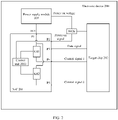
- FIG. 1 is an example of a schematic diagram of a structure of an electronic device.
- an electronic device 100 mainly includes a SoC 101, a TCON chip 102, and a power supply module 103.
- the SoC 101 may include a power supply pin P1, a power supply control pin P2, a data pin P3, a configuration pin P4, and a configuration pin P5.
- the power supply pin P1 is connected to the power supply module 103
- the power supply control pin P2 is connected to a power supply switch MOS
- the data pin P3, the configuration pin P4, and the configuration pin P5 are separately connected to corresponding pins in the TCON chip 102.
- the power supply switch MOS is disposed on a SoC board in which the SoC is located.
- the power supply switch MOS mainly includes a control end, a first end, and a second end.
- the control end of the power supply switch MOS is connected to the power supply control pin P2 of the SoC, the first end of the power supply switch MOS is connected to the power supply module 103, and the second end of the power supply switch MOS is connected to the TCON chip.
- the power supply module 103 may include a battery, a power management unit (power management unit, PMU), a direct-current conversion circuit (direct-current conversion circuit), and the like.
- the power supply module 103 is connected to the SoC 101 and the first end of the power supply switch MOS.
- the power supply module 103 can provide a power supply voltage to the SoC 101.
- the power supply voltage provided by the power supply module 103 to the SoC may be a 3V3 voltage.
- the power supply voltage is 3.3 V
- the voltage may also be another voltage.
- the power supply voltage may also be a 1.8 V voltage.
- the SoC 101 may receive the power supply voltage by using the power supply pin P1, to complete power-on.
- the SoC 101 may continue to control the TCON chip to be powered on. Specifically, the SoC 101 may send a power-on signal to the power supply switch MOS by using the power supply control pin P2. The power-on signal may be used to turn on the power supply switch MOS and connect a path between the power supply module 103 and the TCON chip 102.
- the power supply module 103 outputs a power-on voltage VCC to the power supply switch MOS, and the power-on voltage VCC is transmitted to the TCON chip by using the power supply switch MOS.
- the TCON chip receives the power-on voltage VCC to complete power-on.
- the SoC 101 may continue to send a control signal 1 to the TCON chip by using the configuration pin P4, and send a control signal 2 to the TCON chip by using the configuration pin P5, to control the TCON chip by using the control signal 1 and the control signal 2.
- the SoC 101 may configure the TCON chip by using the control signal 1 and the control signal 2, for example, configure parameters such as a display area and a quantity of bits of the TCON chip.
- the control signal 1 may be a high-level signal corresponding to a digit 1, or may be a low-level signal corresponding to a digit 0.
- the SoC 101 may indicate a specific configuration type of the TOCN chip by using the control signal 1 and the control signal 2.
- the specific configuration type is any one of the four configuration types, so that the TCON chip 102 can complete configuration based on the specific configuration type indicated by the SoC 101.
- the SoC 101 may transmit a data signal Data to the TCON chip 102 by using the data pin P3, so that the TCON chip 102 can control, based on the data signal Data, a display panel to display an image.
- a pull-up resistor R1 corresponding to the configuration pin P4 and a pull-up resistor R2 corresponding to the configuration pin P5 may also be disposed in a peripheral circuit of the SoC 101.
- the pull-up resistor R1 is used as an example. One end of the pull-up resistor R1 is connected to the power supply module 103, and the other end is connected to the configuration pin P4.
- the pull-up resistor R1 may receive a pull-up voltage from the power supply module 103.
- the pull-up resistor R1 may divide the received pull-up voltage, to suppress a voltage of the control signal 1 and protect the TCON chip 102.
- a resistance value of the pull-up resistor R1 is set based on the TCON chip 102, so that when the control signal 1 is a high-level signal, the voltage of the control signal 1 can be identified by the TCON chip 102, and the TCON chip 102 is not damaged due to an excessively large current.
- the pull-up voltage of the pull-up resistor R1 and the power supply voltage of the SoC 101 have a same source. Therefore, when the SoC 101 is powered on, the pull-up resistor R1 also receives the pull-up voltage, and the pull-up resistor R1 may provide a high-level signal for the TCON chip 102.
- the SoC 101 usually does not immediately turn on the power supply switch MOS after being powered on. For example, the SoC 101 needs to first complete initialization, and then turn on the power supply switch MOS. Therefore, when receiving the high-level signal provided by the pull-up resistor R1, the TCON chip 102 is not powered on yet. After receiving the high-level signal provided by the pull-up resistor R1, the TCON chip 102 may make false determining.
- an embodiment of this application provides an integrated circuit.
- the integrated circuit may be a SoC, or may be an integrated circuit having a control function, such as a CPU or a microcontroller unit (microcontroller unit, MCU). This is not limited in this embodiment of this application.
- the SoC is still used as an example for description in the following embodiments of this application.
- FIG. 2 is an example of a schematic diagram of a system structure of an electronic device to which an embodiment of this application is applicable.
- an electronic device 200 includes a SoC 201 and a target chip 202.
- the target chip 202 may be a functional chip controlled by the SoC 201, for example, a baseband chip, a TCON chip, a sensor chip, or another functional chip that is located in a power supply domain different from that of the SoC 201.
- the electronic device 200 may further include a power supply module 203, and the power supply module 203 may supply power to the SoC 201 and the target chip 202.
- the power supply module 203 refer to the power supply module 103. Details are not described herein again.
- the SoC 201 mainly includes a power supply pin P1, configuration pins P4 and P5, switchable pull-up resistors (KR1 and KR2), and a control unit 2011. It should be understood that the SoC 201 may include one or more configuration pins, and each configuration pin corresponds to a switchable pull-up resistor. As shown in FIG. 2 , the configuration pin P4 corresponds to the switchable pull-up resistor KR1, and the configuration pin P5 corresponds to the switchable pull-up resistor KR2. The SoC 201 can provide a control signal for the target chip by using the configuration pins P4 and P5.
- the switchable pull-up resistor KR1 includes a first end, a second end, and a control end.
- the first end of the switchable pull-up resistor KR1 is connected to the power supply pin P1. Therefore, after the SoC 201 receives a power supply voltage by using the power supply pin P1, the power supply voltage may also be used as a pull-up voltage of the switchable pull-up resistor KR1.
- the second end of the switchable pull-up resistor KR1 is connected to the configuration pin P4, and the control end of the switchable pull-up resistor KR1 is connected to the control unit 2011.
- the control unit 2011 may control the switchable pull-up resistor KR1 to be in an off state before the target chip 202 is powered on.
- the SoC 201 may include only one configuration pin, for example, include only the configuration pin P4; or the SoC 201 may include a plurality of configuration pins, for example, include the configuration pins P4 and P5.
- the plurality of configuration pins also correspond to switchable pull-up resistors, and a connection manner between each configuration pin and a corresponding switchable pull-up resistor is similar to that between the configuration pin P4 and the switchable pull-up resistor KR1.
- the configuration pin P5 corresponds to the switchable pull-up resistor KR2.
- the switchable pull-up resistor KR2 includes a first end, a second end, and a control end.
- the first end of the switchable pull-up resistor KR2 is connected to the power supply pin P1. Therefore, after the SoC 201 receives the power supply voltage by using the power supply pin P1, the power supply voltage may also be used as a pull-up voltage of the switchable pull-up resistor KR2.
- the second end of the switchable pull-up resistor KR2 is connected to the configuration pin P5, and the control end of the switchable pull-up resistor KR2 is connected to the control unit 2011.
- the control unit 2011 may control the switchable pull-up resistor KR2 to be in an off state before the target chip 202 is powered on.
- configuration pin P4 and the switchable pull-up resistor KR1 are used as examples for description.
- Another configuration pin (for example, P5) and another switchable pull-up resistor (for example, KR2) in the SoC 201 may have a similar implementation, and details are not described herein again.
- the switchable pull-up resistor KR1 is a controllable switchable resistor.
- the control unit 2011 keeps the switchable pull-up resistor KR1 off before the target chip 202 is powered on, so that the pull-up voltage (the power supply voltage of the SoC 201) received by the switchable pull-up resistor KR1 is not transmitted to the configuration pin P4, and is neither transmitted to the target chip 202. Therefore, this embodiment of this application helps prevent the target chip 202 from receiving an error signal from the configuration pin P4 before the target chip 202 is powered on. In this way, reliability of the SoC 201 is improved.
- the switchable pull-up resistor KR1 is inside the SoC 201, the power supply voltage of the SoC is used to provide the pull-up voltage for the switchable pull-up resistor KR1.
- This implementation helps simplify a structure of a peripheral circuit of the SoC, and reduce a board area occupied by the peripheral circuit and production costs.
- the SoC 201 may send a control signal 1 by using the configuration pin P4.
- a specific implementation of the control signal 1 is mainly determined based on a type of the target chip 202.
- the control signal 1 may be a high-level signal or a low-level signal, to indicate a configuration type to the target chip 202, for example, the foregoing configuration of the TCON chip 102.
- the control signal 1 may also carry configuration information of the target chip 202, for example, a value of each parameter that needs to be configured by the target chip 202; and the target chip 202 may complete configuration based on the configuration information.
- the SoC 201 may further include a switchable pull-down resistor KR3 corresponding to the configuration pin P4.
- the switchable pull-down resistor KR3 includes a first end, a second end, and a control end. The first end of the switchable pull-down resistor KR3 is connected to the configuration pin P4, and the second end of the switchable pull-down resistor KR3 is grounded.
- the control unit 2011 may control the switchable pull-up resistor KR1 to be in an on state or the off state, and control the switchable pull-down resistor KR3 to be in an on state or an off state, to generate the control signal 1. Then, the control signal 1 is output to the target chip by using the configuration pin P4.
- the control signal 1 when the switchable pull-up resistor KR1 is in the on state, and the switchable pull-down resistor KR3 is in the off state, the control signal 1 is at a high level.
- the control signal 1 is at a low level. Therefore, the control unit 2011 may control the switchable pull-up resistor KR1 to be in the on state or the off state and control the switchable pull-down resistor KR3 to be in the on state or the off state, to generate the control signal 1.
- a resistance value of the switchable pull-up resistor KR1 may be adapted to the target chip. In this way, when the control signal 1 is at the high level, the control signal 1 can be identified by the target chip 202, and the target chip 202 is not damaged due to an excessively large current.
- the resistance value of the switchable pull-up resistor may include any resistance value from 4.7 k ⁇ to 10 k ⁇ .
- the switchable pull-up resistor KR1 includes a pull-up switch Ku and a pull-up resistor Ru.
- the pull-up switch Ku includes the first end, a second end, and the control end.
- the first end of the pull-up switch Ku is connected to the configuration pin P4
- the second end of the pull-up switch Ku is connected to one end of the pull-up resistor Ru
- the control end of the pull-up switch Ku is connected to the control unit 2011, and the other end of the pull-up resistor Ru is connected to the power supply pin P1.
- the control end of the pull-up switch Ku is the control end of the switchable pull-up resistor KR1.
- the control unit 2011 may turn on the pull-up switch Ku, to control the switchable pull-up resistor KR1 to be in the on state.
- the control unit 2011 may also turn off the pull-up switch Ku, to control the switchable pull-up resistor KR1 to be in the off state.
- a resistance value of the pull-up resistor Ru is the resistance value of the switchable pull-up resistor KR1.
- the resistance value of the pull-up resistor Ru may be adapted to the target chip 202.
- the resistance value of the pull-up resistor Ru may include any resistance value from 4.7 k ⁇ to 10 k ⁇ .
- the switchable pull-down resistor KR3 may include a pull-down switch Kd and a pull-down resistor Rd.
- the pull-down switch Kd includes the first end, a second end, and the control end.
- the first end of the pull-down switch Kd is connected to the configuration pin P4
- the second end of the pull-down switch Kd is connected to one end of the pull-down resistor Rd
- the control end of the pull-down switch Kd is connected to the control unit 2011, and the other end of the pull-down resistor Rd is grounded.
- the control end of the pull-down switch Kd is the control end of the switchable pull-down resistor KR3.
- the control unit 2011 may turn on the pull-down switch Kd, to control the switchable pull-down resistor KR3 to be in the on state.
- the control unit 2011 may also turn off the pull-down switch Kd, to control the switchable pull-down resistor KR3 to be in the off state.
- the pull-down resistor Rd has a large resistance value. This can reduce a magnitude of a current that passes through the switchable pull-down resistor KR3 when the pull-down switch Kd is turned on, and helps protect the pull-down switch Kd.
- control unit 2011 may control the switchable pull-up resistor KR1 to be in the off state before the target chip 202 is powered on. It should be understood that, before the target chip is powered on, the switchable pull-up resistor KR1 keeps being in the off state.
- the control unit 2011 may output a power-on signal by using the power supply control pin P2.
- the power-on signal may be used to connect a path for powering on the target chip 202.
- the power-on signal may be used to turn on the power supply switch MOS, so that a path between the power supply module 203 and the target chip 202 is connected, and the power-on voltage output by the power supply module 203 can be transmitted to the target chip 202.
- the power-on voltage gradually increases from a low initial voltage to a target voltage. It may be considered that the target chip 202 completes power-on only after the power-on voltage is stabilized at the target voltage.
- control unit 2011 may control the switchable pull-up resistor KR1 to be in the off state before a target time point.
- the target time point is not earlier than a time point at which the power-on voltage of the target chip 202 reaches the target voltage, namely, a time point at which the target chip 202 completes power-on.
- control unit 2011 may calculate the target time point based on a time point of outputting the power-on signal and a delay for the power-on voltage of the target chip 202 to reach the target voltage.
- a delay between a time point at which the target chip 202 starts to be powered on and the time point at which the power-on voltage of the target chip 202 reaches the target voltage is a power-on delay of the target chip 202.
- the power-on delay may be preset in the SoC 201.
- control unit 2011 may also start timing after outputting the power-on signal. Before timing duration reaches a first delay, the switchable pull-up resistor KR1 is controlled to be in the off state. A time length of the first delay is not less than that of the power-on delay of the target chip 202.
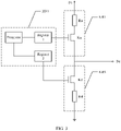
- control unit 2011 may include a processor and one or more registers.
- the processor and the registers may be integrated into a same module, or may be disposed independently. This is not limited in this embodiment of this application.
- the one or more registers in the control unit 2011 one-to-one correspond to switchable resistors controlled by the control unit 2011.
- the control unit 2011 includes a register 1 and a register 2.
- the register 1 corresponds to the switchable pull-up resistor KR1, in other words, the register 1 is connected to the control end of the switchable pull-up resistor KR1.
- the register 2 corresponds to the switchable pull-down resistor KR3, in other words, the register 2 is connected to the control end of the switchable pull-down resistor KR3.
- the SoC 201 may include N switchable pull-up resistors (KR11 to KR1N, where N is an integer greater than 1) that correspond to the configuration pin P4.
- the control unit 2011 includes registers 11 to IN and the register 2.
- the register 11 to the register IN correspond to the switchable pull-up resistors KR11 to KR1N, and the register 2 corresponds to the switchable pull-down resistor KR3.
- the processor and the register 1 in FIG. 3 are used as examples.
- the processor may write control information of the switchable pull-up resistor KR1 into the register 1.
- the register 1 then generates a drive signal based on the control information of the switchable pull-up resistor KR1, where the drive signal may control the switchable pull-up resistor KR1 to be on or off.
- the processor may write data 1 into the register 1.
- the register 1 generates a drive signal a based on the written data 1, and provides the drive signal a for the switchable pull-up resistor KR1, to turn on the switchable pull-up resistor KR1.
- the processor may write data 0 into the register 1.
- the register 1 generates a drive signal b based on the written data 0, and provides the drive signal b for the switchable pull-up resistor KR1, to turn off the switchable pull-up resistor KR1.
- control unit 2011 controls another switchable resistor is similar to that of the switchable pull-up resistor KR1, and details are not described herein again.
- the N switchable pull-up resistors in the SoC 201 are connected in parallel between the power supply pin P1 and the configuration pin P4.
- the control unit 2011 may determine one or more target switchable pull-up resistors in the N switchable pull-up resistors, control the one or more target switchable pull-up resistors to be in an on state or an off state, and control the switchable pull-down resistor KR3 to be in the on state or off state, to generate the control signal 1.
- resistance values of the N switchable pull-up resistors may be set based on a possible type of the target chip 202. Resistance values of different switchable pull-up resistors may be the same or may be different.
- information about the target switchable pull-up resistors may be set for the SoC 201 based on the target chip 202.
- the control unit 2011 may determine the one or more target switchable pull-up resistors in the N switchable pull-up resistors based on the information about the target switchable pull-up resistors.
- the target switchable pull-up resistor can adjust a high-level voltage of the control signal 1.
- the target switchable pull-up resistor can adjust the high-level voltage of the control signal 1.
- an embodiment of this application further provides a control method.
- the method may be used in an integrated circuit.
- the integrated circuit may be the integrated circuit (SoC) provided in any one of the foregoing embodiments. Details are not described in this embodiment of this application again.
- FIG. 5 is an example of a schematic flowchart of a control method according to an embodiment of this application. As shown in FIG. 5 , the method mainly includes the following steps.
- S501 Receive a power supply voltage by using a power supply pin.
- S502 Control a switchable pull-up resistor to be in an off state before a target chip is powered on.
- the switchable pull-up resistor is a controllable switchable resistor, and an integrated circuit keeps the switchable pull-up resistor off before the target chip is powered on, so that a pull-up voltage (namely, a power supply voltage of the integrated circuit) received by the switchable pull-up resistor is not transmitted to a configuration pin, and is neither transmitted to the target chip. Therefore, this embodiment of this application helps prevent the target chip from receiving an error signal from the configuration pin before the target chip is powered on. In this way, reliability of the integrated circuit is improved.
- the switchable pull-up resistor in this application is inside the integrated circuit, the power supply voltage of the integrated circuit is used to provide the pull-up voltage for the switchable pull-up resistor.
- This implementation helps simplify a structure of a peripheral circuit of the integrated circuit, and reduce a board area occupied by the peripheral circuit and production costs.
- the integrated circuit may determine, based on a target time point, whether to continue to control the switchable pull-up resistor to be in the off state.
- the target time point is not earlier than a time point at which a power-on voltage of the target chip reaches a target voltage.
- the integrated circuit may control the switchable pull-up resistor to be in the off state before the target time point.
- the integrated circuit may further output a power-on signal by using a power supply control pin, where the power-on signal is used to connect a path for powering on the target chip; and calculate the target time point based on a time point of outputting the power-on signal and a delay for the power-on voltage of the target chip to reach the target voltage.
- the integrated circuit may further include a switchable pull-down resistor.
- a first end of the switchable pull-down resistor is connected to the configuration pin, and a second end of the switchable pull-down resistor is grounded.
- the integrated circuit may further control the switchable pull-up resistor to be in an on state or the off state, and control the switchable pull-down resistor to be in an on state or an off state, to generate a control signal; and output the control signal to the target chip by using the configuration pin.
- the integrated circuit provided in this embodiment of this application may include a plurality of switchable pull-up resistors connected in parallel.
- the integrated circuit when generating the control signal, the integrated circuit may determine one or more target switchable pull-up resistors in the plurality of switchable pull-up resistors.
- the integrated circuit may further control the one or more target switchable pull-up resistors to be in an on state or an off state.
- FIG. 6 is a schematic flowchart of a control method according to an embodiment of this application. As shown in FIG. 6 , the control method mainly includes the following steps.
- S601 Power on the SoC 201.
- the SoC 201 may receive, by using the power supply pin P1, the power supply voltage provided by the power supply module 203, to complete power-on.
- the SoC 201 may further perform an operation such as initialization.
- the SoC 201 controls the switchable pull-up resistors KR1 and KR2 to be in the off state.
- the SoC 201 outputs the power-on signal. Specifically, the SoC 201 may output the power-on signal to the power supply switch MOS by using the power supply control pin P2. The power-on signal may be used to turn on the power supply switch MOS, so that the path between the power supply module 203 and the target chip 202 is connected, and the power-on voltage output by the power supply module 203 can be transmitted to the target chip 202.
- the SoC 201 controls the switchable pull-up resistors KR1 and KR2 to be in the off state.
- the SoC 201 waits for the first delay.
- the time length of the first delay is not less than that of the power-on delay of the target chip 202.
- the SoC 201 outputs the power-on signal, it may be considered that the target chip 202 starts to be powered on.
- the SoC 201 controls the switchable pull-up resistors KR1 and KR2 to be in the off state.
- the SoC 201 outputs the control signal.
- the SoC 201 may control the switchable pull-up resistor KR1 to be in the on state or the off state, to generate the control signal 1.
- the SoC 201 may control the switchable pull-up resistor KR2 to be in the on state or the off state, to generate the control signal 2. Therefore, the SoC 201 may control the target chip 202 by using the control signal 1 and the control signal 2.
- this application may be provided as a method, a system, or a computer program product. Therefore, this application may use a form of hardware only embodiments, software only embodiments, or embodiments with a combination of software and hardware. Moreover, this application may use a form of a computer program product that is implemented on one or more computer-usable storage media (including but not limited to a disk memory, a CD-ROM, an optical memory, and the like) that include computer usable program code.
- a computer-usable storage media including but not limited to a disk memory, a CD-ROM, an optical memory, and the like
- These computer program instructions may be provided for a general-purpose computer, a dedicated computer, an embedded processor, or a processor of any other programmable data processing device to generate a machine, so that the instructions executed by a computer or the processor of any other programmable data processing device generate an apparatus for implementing a specific function in one or more processes in the flowcharts and/or in one or more blocks in the block diagrams.
- These computer program instructions may be saved in a computer-readable memory that can indicate the computer or any other programmable data processing device to work in a specific manner, so that the instructions saved in the computer-readable memory generate an artifact that includes an instruction apparatus.
- the instruction apparatus implements a specific function in one or more processes in the flowcharts and/or in one or more blocks in the block diagrams.
- These computer program instructions may be loaded onto a computer or another programmable data processing device, so that a series of operations and steps are performed on the computer or the another programmable device, to generate computer-implemented processing. Therefore, the instructions executed on the computer or the another programmable device provide steps for implementing a specific function in one or more processes in the flowcharts and/or in one or more blocks in the block diagrams.
Applications Claiming Priority (1)
| Application Number | Priority Date | Filing Date | Title |
|---|---|---|---|
| PCT/CN2020/075421 WO2021159526A1 (zh) | 2020-02-14 | 2020-02-14 | 一种集成电路、控制方法及系统 |
Publications (2)
| Publication Number | Publication Date |
|---|---|
| EP4099566A1 true EP4099566A1 (de) | 2022-12-07 |
| EP4099566A4 EP4099566A4 (de) | 2023-01-25 |
Family
ID=77292952
Family Applications (1)
| Application Number | Title | Priority Date | Filing Date |
|---|---|---|---|
| EP20918402.7A Pending EP4099566A4 (de) | 2020-02-14 | 2020-02-14 | Integrierte schaltung und steuerverfahren und -system |
Country Status (4)
| Country | Link |
|---|---|
| US (1) | US11855616B2 (de) |
| EP (1) | EP4099566A4 (de) |
| CN (1) | CN115104259A (de) |
| WO (1) | WO2021159526A1 (de) |
Family Cites Families (15)
| Publication number | Priority date | Publication date | Assignee | Title |
|---|---|---|---|---|
| KR100729916B1 (ko) * | 2004-04-08 | 2007-06-18 | 주식회사 하이닉스반도체 | 온 다이 터미네이션 회로 |
| JP4337711B2 (ja) * | 2004-11-17 | 2009-09-30 | 株式会社デンソー | 半導体素子制御装置 |
| US7921231B2 (en) * | 2008-01-04 | 2011-04-05 | Silicon Image, Inc. | Discovery of electronic devices utilizing a control bus |
| DE102009052947B3 (de) * | 2009-11-12 | 2010-12-16 | Sinitec Vertriebsgesellschaft Mbh | Energiesparschaltung für ein Peripheriegerät, Peripheriegerät, Vermittlungsgerät und Arbeitsverfahren |
| JP5671269B2 (ja) * | 2010-06-24 | 2015-02-18 | ラピスセミコンダクタ株式会社 | バス接続回路を備えた半導体装置及びそのバス接続方法 |
| CN103545784B (zh) * | 2012-07-12 | 2017-04-12 | 上海电科电器科技有限公司 | 控制与保护开关电器的脉冲控制器 |
| KR102226370B1 (ko) * | 2015-01-13 | 2021-03-15 | 삼성전자주식회사 | 집적 회로 및 집적 회로를 포함하는 스토리지 장치 |
| US10386913B2 (en) * | 2016-04-01 | 2019-08-20 | Platina Systems Corporation | Priority based power-off during partial power loss |
| US10289589B2 (en) * | 2016-08-31 | 2019-05-14 | Intel Corporation | Apparatuses to resolve roles for dual role serial bus devices |
| CN206251066U (zh) * | 2016-12-13 | 2017-06-13 | 深圳Tcl数字技术有限公司 | 芯片复位电路及电子设备 |
| US10141045B2 (en) * | 2016-12-15 | 2018-11-27 | Taiwan Semiconductor Manufacturing Co., Ltd. | Dual rail device with power detector for controlling power to first and second power domains |
| CN106685023B (zh) * | 2017-03-28 | 2019-03-29 | 湖南科技大学 | 仪器内部供电串联电池组的平衡管理模块 |
| CN106787031B (zh) * | 2017-03-28 | 2019-03-29 | 湖南科技大学 | 一种串联电池组快平衡充电装置 |
| US10637462B1 (en) * | 2019-05-30 | 2020-04-28 | Xilinx, Inc. | System and method for SoC power-up sequencing |
| TWI715498B (zh) * | 2020-05-19 | 2021-01-01 | 瑞昱半導體股份有限公司 | 連接埠控制裝置 |
-
2020
- 2020-02-14 CN CN202080096598.2A patent/CN115104259A/zh active Pending
- 2020-02-14 EP EP20918402.7A patent/EP4099566A4/de active Pending
- 2020-02-14 WO PCT/CN2020/075421 patent/WO2021159526A1/zh unknown
-
2022
- 2022-08-12 US US17/887,176 patent/US11855616B2/en active Active
Also Published As
| Publication number | Publication date |
|---|---|
| WO2021159526A1 (zh) | 2021-08-19 |
| US11855616B2 (en) | 2023-12-26 |
| EP4099566A4 (de) | 2023-01-25 |
| US20220393677A1 (en) | 2022-12-08 |
| CN115104259A (zh) | 2022-09-23 |
Similar Documents
| Publication | Publication Date | Title |
|---|---|---|
| CN105786421B (zh) | 一种服务器显示方法及装置 | |
| US10042801B2 (en) | System for detecting universal serial bus (USB) device and method thereof | |
| US9716497B2 (en) | Calibration circuit and calibration apparatus including the same | |
| CN108205393B (zh) | 半导体设备、人机接口设备及电子装置 | |
| US20140118330A1 (en) | Display device and method for driving the same | |
| GB2373080A (en) | Providing USB device identification information | |
| US10504478B2 (en) | Semiconductor device having shifted operation voltages in different modes and electronic apparatus thereof | |
| CN110444156B (zh) | 显示装置及其驱动器 | |
| CN111800658B (zh) | 一种芯片参数写入方法、电视机及存储介质 | |
| CN108446139B (zh) | 一种fpga芯片的唤醒方法及装置 | |
| JP2003241730A (ja) | 表示装置 | |
| EP3002701A1 (de) | Verfahren und vorrichtung zur programmdatenaktualisierung | |
| US8994445B2 (en) | Electronic device | |
| US20160342800A1 (en) | Electronic device and hard disk device of electronic device | |
| EP4099566A1 (de) | Integrierte schaltung und steuerverfahren und -system | |
| US11289040B2 (en) | Driving circuit and driving method of liquid crystal display | |
| US10977206B2 (en) | Data communication device and method for data communication | |
| CN112750389A (zh) | 测试装置 | |
| KR102352751B1 (ko) | 터치표시장치 및 그 구동방법 | |
| CN210270878U (zh) | 显示器主板及显示器 | |
| US6530048B1 (en) | I2C test single chip | |
| JP5897866B2 (ja) | 電源回路、及び液晶表示装置 | |
| CN103634642A (zh) | 一种降低功耗的方法及装置 | |
| KR102611839B1 (ko) | 반도체 칩 및 이를 포함하는 전자 장치 | |
| JP6360320B2 (ja) | 半導体装置 |
Legal Events
| Date | Code | Title | Description |
|---|---|---|---|
| STAA | Information on the status of an ep patent application or granted ep patent |
Free format text: STATUS: THE INTERNATIONAL PUBLICATION HAS BEEN MADE |
|
| PUAI | Public reference made under article 153(3) epc to a published international application that has entered the european phase |
Free format text: ORIGINAL CODE: 0009012 |
|
| STAA | Information on the status of an ep patent application or granted ep patent |
Free format text: STATUS: REQUEST FOR EXAMINATION WAS MADE |
|
| 17P | Request for examination filed |
Effective date: 20220902 |
|
| AK | Designated contracting states |
Kind code of ref document: A1 Designated state(s): AL AT BE BG CH CY CZ DE DK EE ES FI FR GB GR HR HU IE IS IT LI LT LU LV MC MK MT NL NO PL PT RO RS SE SI SK SM TR |
|
| A4 | Supplementary search report drawn up and despatched |
Effective date: 20230103 |
|
| RIC1 | Information provided on ipc code assigned before grant |
Ipc: H03K 19/0175 20060101ALI20221221BHEP Ipc: G06F 1/24 20060101ALI20221221BHEP Ipc: H02J 7/00 20060101ALI20221221BHEP Ipc: H03K 17/22 20060101AFI20221221BHEP |
|
| DAV | Request for validation of the european patent (deleted) | ||
| DAX | Request for extension of the european patent (deleted) | ||
| STAA | Information on the status of an ep patent application or granted ep patent |
Free format text: STATUS: EXAMINATION IS IN PROGRESS |
|
| 17Q | First examination report despatched |
Effective date: 20240313 |