EP4047762A1 - Creating arbitrary patterns on a 2-d uniform grid vcsel array - Google Patents
Creating arbitrary patterns on a 2-d uniform grid vcsel array Download PDFInfo
- Publication number
- EP4047762A1 EP4047762A1 EP22159829.5A EP22159829A EP4047762A1 EP 4047762 A1 EP4047762 A1 EP 4047762A1 EP 22159829 A EP22159829 A EP 22159829A EP 4047762 A1 EP4047762 A1 EP 4047762A1
- Authority
- EP
- European Patent Office
- Prior art keywords
- optoelectronic
- cells
- optoelectronic cells
- epitaxial layers
- array
- Prior art date
- Legal status (The legal status is an assumption and is not a legal conclusion. Google has not performed a legal analysis and makes no representation as to the accuracy of the status listed.)
- Granted
Links
Images



Classifications
-
- H—ELECTRICITY
- H01—ELECTRIC ELEMENTS
- H01S—DEVICES USING THE PROCESS OF LIGHT AMPLIFICATION BY STIMULATED EMISSION OF RADIATION [LASER] TO AMPLIFY OR GENERATE LIGHT; DEVICES USING STIMULATED EMISSION OF ELECTROMAGNETIC RADIATION IN WAVE RANGES OTHER THAN OPTICAL
- H01S5/00—Semiconductor lasers
- H01S5/10—Construction or shape of the optical resonator, e.g. extended or external cavity, coupled cavities, bent-guide, varying width, thickness or composition of the active region
- H01S5/18—Surface-emitting [SE] lasers, e.g. having both horizontal and vertical cavities
- H01S5/183—Surface-emitting [SE] lasers, e.g. having both horizontal and vertical cavities having only vertical cavities, e.g. vertical cavity surface-emitting lasers [VCSEL]
- H01S5/18308—Surface-emitting [SE] lasers, e.g. having both horizontal and vertical cavities having only vertical cavities, e.g. vertical cavity surface-emitting lasers [VCSEL] having a special structure for lateral current or light confinement
- H01S5/18322—Position of the structure
- H01S5/18327—Structure being part of a DBR
-
- H—ELECTRICITY
- H01—ELECTRIC ELEMENTS
- H01S—DEVICES USING THE PROCESS OF LIGHT AMPLIFICATION BY STIMULATED EMISSION OF RADIATION [LASER] TO AMPLIFY OR GENERATE LIGHT; DEVICES USING STIMULATED EMISSION OF ELECTROMAGNETIC RADIATION IN WAVE RANGES OTHER THAN OPTICAL
- H01S5/00—Semiconductor lasers
- H01S5/02—Structural details or components not essential to laser action
- H01S5/026—Monolithically integrated components, e.g. waveguides, monitoring photo-detectors, drivers
-
- H—ELECTRICITY
- H01—ELECTRIC ELEMENTS
- H01S—DEVICES USING THE PROCESS OF LIGHT AMPLIFICATION BY STIMULATED EMISSION OF RADIATION [LASER] TO AMPLIFY OR GENERATE LIGHT; DEVICES USING STIMULATED EMISSION OF ELECTROMAGNETIC RADIATION IN WAVE RANGES OTHER THAN OPTICAL
- H01S5/00—Semiconductor lasers
- H01S5/04—Processes or apparatus for excitation, e.g. pumping, e.g. by electron beams
- H01S5/042—Electrical excitation ; Circuits therefor
- H01S5/0425—Electrodes, e.g. characterised by the structure
- H01S5/04256—Electrodes, e.g. characterised by the structure characterised by the configuration
-
- H—ELECTRICITY
- H01—ELECTRIC ELEMENTS
- H01S—DEVICES USING THE PROCESS OF LIGHT AMPLIFICATION BY STIMULATED EMISSION OF RADIATION [LASER] TO AMPLIFY OR GENERATE LIGHT; DEVICES USING STIMULATED EMISSION OF ELECTROMAGNETIC RADIATION IN WAVE RANGES OTHER THAN OPTICAL
- H01S5/00—Semiconductor lasers
- H01S5/10—Construction or shape of the optical resonator, e.g. extended or external cavity, coupled cavities, bent-guide, varying width, thickness or composition of the active region
- H01S5/12—Construction or shape of the optical resonator, e.g. extended or external cavity, coupled cavities, bent-guide, varying width, thickness or composition of the active region the resonator having a periodic structure, e.g. in distributed feedback [DFB] lasers
-
- H—ELECTRICITY
- H01—ELECTRIC ELEMENTS
- H01S—DEVICES USING THE PROCESS OF LIGHT AMPLIFICATION BY STIMULATED EMISSION OF RADIATION [LASER] TO AMPLIFY OR GENERATE LIGHT; DEVICES USING STIMULATED EMISSION OF ELECTROMAGNETIC RADIATION IN WAVE RANGES OTHER THAN OPTICAL
- H01S5/00—Semiconductor lasers
- H01S5/10—Construction or shape of the optical resonator, e.g. extended or external cavity, coupled cavities, bent-guide, varying width, thickness or composition of the active region
- H01S5/18—Surface-emitting [SE] lasers, e.g. having both horizontal and vertical cavities
- H01S5/183—Surface-emitting [SE] lasers, e.g. having both horizontal and vertical cavities having only vertical cavities, e.g. vertical cavity surface-emitting lasers [VCSEL]
- H01S5/18308—Surface-emitting [SE] lasers, e.g. having both horizontal and vertical cavities having only vertical cavities, e.g. vertical cavity surface-emitting lasers [VCSEL] having a special structure for lateral current or light confinement
-
- H—ELECTRICITY
- H01—ELECTRIC ELEMENTS
- H01S—DEVICES USING THE PROCESS OF LIGHT AMPLIFICATION BY STIMULATED EMISSION OF RADIATION [LASER] TO AMPLIFY OR GENERATE LIGHT; DEVICES USING STIMULATED EMISSION OF ELECTROMAGNETIC RADIATION IN WAVE RANGES OTHER THAN OPTICAL
- H01S5/00—Semiconductor lasers
- H01S5/10—Construction or shape of the optical resonator, e.g. extended or external cavity, coupled cavities, bent-guide, varying width, thickness or composition of the active region
- H01S5/18—Surface-emitting [SE] lasers, e.g. having both horizontal and vertical cavities
- H01S5/183—Surface-emitting [SE] lasers, e.g. having both horizontal and vertical cavities having only vertical cavities, e.g. vertical cavity surface-emitting lasers [VCSEL]
- H01S5/18308—Surface-emitting [SE] lasers, e.g. having both horizontal and vertical cavities having only vertical cavities, e.g. vertical cavity surface-emitting lasers [VCSEL] having a special structure for lateral current or light confinement
- H01S5/18311—Surface-emitting [SE] lasers, e.g. having both horizontal and vertical cavities having only vertical cavities, e.g. vertical cavity surface-emitting lasers [VCSEL] having a special structure for lateral current or light confinement using selective oxidation
-
- H—ELECTRICITY
- H01—ELECTRIC ELEMENTS
- H01S—DEVICES USING THE PROCESS OF LIGHT AMPLIFICATION BY STIMULATED EMISSION OF RADIATION [LASER] TO AMPLIFY OR GENERATE LIGHT; DEVICES USING STIMULATED EMISSION OF ELECTROMAGNETIC RADIATION IN WAVE RANGES OTHER THAN OPTICAL
- H01S5/00—Semiconductor lasers
- H01S5/10—Construction or shape of the optical resonator, e.g. extended or external cavity, coupled cavities, bent-guide, varying width, thickness or composition of the active region
- H01S5/18—Surface-emitting [SE] lasers, e.g. having both horizontal and vertical cavities
- H01S5/183—Surface-emitting [SE] lasers, e.g. having both horizontal and vertical cavities having only vertical cavities, e.g. vertical cavity surface-emitting lasers [VCSEL]
- H01S5/18308—Surface-emitting [SE] lasers, e.g. having both horizontal and vertical cavities having only vertical cavities, e.g. vertical cavity surface-emitting lasers [VCSEL] having a special structure for lateral current or light confinement
- H01S5/18322—Position of the structure
- H01S5/1833—Position of the structure with more than one structure
- H01S5/18333—Position of the structure with more than one structure only above the active layer
-
- H—ELECTRICITY
- H01—ELECTRIC ELEMENTS
- H01S—DEVICES USING THE PROCESS OF LIGHT AMPLIFICATION BY STIMULATED EMISSION OF RADIATION [LASER] TO AMPLIFY OR GENERATE LIGHT; DEVICES USING STIMULATED EMISSION OF ELECTROMAGNETIC RADIATION IN WAVE RANGES OTHER THAN OPTICAL
- H01S5/00—Semiconductor lasers
- H01S5/10—Construction or shape of the optical resonator, e.g. extended or external cavity, coupled cavities, bent-guide, varying width, thickness or composition of the active region
- H01S5/18—Surface-emitting [SE] lasers, e.g. having both horizontal and vertical cavities
- H01S5/183—Surface-emitting [SE] lasers, e.g. having both horizontal and vertical cavities having only vertical cavities, e.g. vertical cavity surface-emitting lasers [VCSEL]
- H01S5/18361—Structure of the reflectors, e.g. hybrid mirrors
- H01S5/18369—Structure of the reflectors, e.g. hybrid mirrors based on dielectric materials
-
- H—ELECTRICITY
- H01—ELECTRIC ELEMENTS
- H01S—DEVICES USING THE PROCESS OF LIGHT AMPLIFICATION BY STIMULATED EMISSION OF RADIATION [LASER] TO AMPLIFY OR GENERATE LIGHT; DEVICES USING STIMULATED EMISSION OF ELECTROMAGNETIC RADIATION IN WAVE RANGES OTHER THAN OPTICAL
- H01S5/00—Semiconductor lasers
- H01S5/10—Construction or shape of the optical resonator, e.g. extended or external cavity, coupled cavities, bent-guide, varying width, thickness or composition of the active region
- H01S5/18—Surface-emitting [SE] lasers, e.g. having both horizontal and vertical cavities
- H01S5/185—Surface-emitting [SE] lasers, e.g. having both horizontal and vertical cavities having only horizontal cavities, e.g. horizontal cavity surface-emitting lasers [HCSEL]
- H01S5/187—Surface-emitting [SE] lasers, e.g. having both horizontal and vertical cavities having only horizontal cavities, e.g. horizontal cavity surface-emitting lasers [HCSEL] using Bragg reflection
-
- H—ELECTRICITY
- H01—ELECTRIC ELEMENTS
- H01S—DEVICES USING THE PROCESS OF LIGHT AMPLIFICATION BY STIMULATED EMISSION OF RADIATION [LASER] TO AMPLIFY OR GENERATE LIGHT; DEVICES USING STIMULATED EMISSION OF ELECTROMAGNETIC RADIATION IN WAVE RANGES OTHER THAN OPTICAL
- H01S5/00—Semiconductor lasers
- H01S5/20—Structure or shape of the semiconductor body to guide the optical wave ; Confining structures perpendicular to the optical axis, e.g. index or gain guiding, stripe geometry, broad area lasers, gain tailoring, transverse or lateral reflectors, special cladding structures, MQW barrier reflection layers
- H01S5/2054—Methods of obtaining the confinement
- H01S5/2059—Methods of obtaining the confinement by means of particular conductivity zones, e.g. obtained by particle bombardment or diffusion
- H01S5/2063—Methods of obtaining the confinement by means of particular conductivity zones, e.g. obtained by particle bombardment or diffusion obtained by particle bombardment
-
- H—ELECTRICITY
- H01—ELECTRIC ELEMENTS
- H01S—DEVICES USING THE PROCESS OF LIGHT AMPLIFICATION BY STIMULATED EMISSION OF RADIATION [LASER] TO AMPLIFY OR GENERATE LIGHT; DEVICES USING STIMULATED EMISSION OF ELECTROMAGNETIC RADIATION IN WAVE RANGES OTHER THAN OPTICAL
- H01S5/00—Semiconductor lasers
- H01S5/30—Structure or shape of the active region; Materials used for the active region
- H01S5/34—Structure or shape of the active region; Materials used for the active region comprising quantum well or superlattice structures, e.g. single quantum well [SQW] lasers, multiple quantum well [MQW] lasers or graded index separate confinement heterostructure [GRINSCH] lasers
-
- H—ELECTRICITY
- H01—ELECTRIC ELEMENTS
- H01S—DEVICES USING THE PROCESS OF LIGHT AMPLIFICATION BY STIMULATED EMISSION OF RADIATION [LASER] TO AMPLIFY OR GENERATE LIGHT; DEVICES USING STIMULATED EMISSION OF ELECTROMAGNETIC RADIATION IN WAVE RANGES OTHER THAN OPTICAL
- H01S5/00—Semiconductor lasers
- H01S5/40—Arrangement of two or more semiconductor lasers, not provided for in groups H01S5/02 - H01S5/30
- H01S5/42—Arrays of surface emitting lasers
- H01S5/423—Arrays of surface emitting lasers having a vertical cavity
-
- H—ELECTRICITY
- H10—SEMICONDUCTOR DEVICES; ELECTRIC SOLID-STATE DEVICES NOT OTHERWISE PROVIDED FOR
- H10D—INORGANIC ELECTRIC SEMICONDUCTOR DEVICES
- H10D62/00—Semiconductor bodies, or regions thereof, of devices having potential barriers
- H10D62/80—Semiconductor bodies, or regions thereof, of devices having potential barriers characterised by the materials
- H10D62/81—Semiconductor bodies, or regions thereof, of devices having potential barriers characterised by the materials of structures exhibiting quantum-confinement effects, e.g. single quantum wells; of structures having periodic or quasi-periodic potential variation
- H10D62/815—Semiconductor bodies, or regions thereof, of devices having potential barriers characterised by the materials of structures exhibiting quantum-confinement effects, e.g. single quantum wells; of structures having periodic or quasi-periodic potential variation of structures having periodic or quasi-periodic potential variation, e.g. superlattices or multiple quantum wells [MQW]
- H10D62/8161—Semiconductor bodies, or regions thereof, of devices having potential barriers characterised by the materials of structures exhibiting quantum-confinement effects, e.g. single quantum wells; of structures having periodic or quasi-periodic potential variation of structures having periodic or quasi-periodic potential variation, e.g. superlattices or multiple quantum wells [MQW] potential variation due to variations in composition or crystallinity, e.g. heterojunction superlattices
- H10D62/8162—Semiconductor bodies, or regions thereof, of devices having potential barriers characterised by the materials of structures exhibiting quantum-confinement effects, e.g. single quantum wells; of structures having periodic or quasi-periodic potential variation of structures having periodic or quasi-periodic potential variation, e.g. superlattices or multiple quantum wells [MQW] potential variation due to variations in composition or crystallinity, e.g. heterojunction superlattices having quantum effects only in the vertical direction, i.e. layered structures having quantum effects solely resulting from vertical potential variation
-
- H—ELECTRICITY
- H01—ELECTRIC ELEMENTS
- H01S—DEVICES USING THE PROCESS OF LIGHT AMPLIFICATION BY STIMULATED EMISSION OF RADIATION [LASER] TO AMPLIFY OR GENERATE LIGHT; DEVICES USING STIMULATED EMISSION OF ELECTROMAGNETIC RADIATION IN WAVE RANGES OTHER THAN OPTICAL
- H01S2301/00—Functional characteristics
- H01S2301/17—Semiconductor lasers comprising special layers
- H01S2301/176—Specific passivation layers on surfaces other than the emission facet
-
- H—ELECTRICITY
- H01—ELECTRIC ELEMENTS
- H01S—DEVICES USING THE PROCESS OF LIGHT AMPLIFICATION BY STIMULATED EMISSION OF RADIATION [LASER] TO AMPLIFY OR GENERATE LIGHT; DEVICES USING STIMULATED EMISSION OF ELECTROMAGNETIC RADIATION IN WAVE RANGES OTHER THAN OPTICAL
- H01S5/00—Semiconductor lasers
- H01S5/04—Processes or apparatus for excitation, e.g. pumping, e.g. by electron beams
- H01S5/042—Electrical excitation ; Circuits therefor
- H01S5/0425—Electrodes, e.g. characterised by the structure
Definitions
- the present invention relates generally to optoelectronic devices, and particularly to devices configurable to emit patterned illumination.
- Imaging devices also commonly known as depth sensors or depth mappers, enable the remote measurement of distance (and often intensity) of each point on a target scene - so-called target scene depth - by illuminating the target scene with one or more optical beams and analyzing the reflected optical signal.
- an optoelectronic device comprises a semiconductor die on which a monolithic array of vertical-cavity surface-emitting laser (VCSEL) diodes is formed in a two-dimensional pattern that is not a regular lattice.
- VCSEL vertical-cavity surface-emitting laser
- regular lattice means a two-dimensional pattern in which the spacing between adjacent elements in the pattern (for example, between adjacent emitters in a VCSEL array) is constant and is synonymous with a periodic lattice.
- the pattern can be uncorrelated, in the sense that the auto-correlation of the positions of the laser diodes as a function of transverse shift is insignificant for any shift larger than the diode size. Random, pseudo-random, and quasi-periodic patterns are examples of such uncorrelated patterns.
- Embodiments of the present invention that are described hereinbelow provide improved methods for fabricating patterned light sources and light sources that can be produced by such methods.
- an optoelectronic device including a semiconductor substrate and an array of optoelectronic cells, which are formed on the semiconductor substrate.
- the cells include first epitaxial layers defining a lower distributed Bragg-reflector (DBR) stack; second epitaxial layers formed over the lower DBR stack, defining a quantum well structure; third epitaxial layers, formed over the quantum well structure, defining an upper DBR stack; and electrodes formed over the upper DBR stack, which are configurable to inject an excitation current into the quantum well structure of each optoelectronic cell.
- DBR distributed Bragg-reflector
- the array includes a first set of the optoelectronic cells that are configured to emit laser radiation in response to the excitation current and a second set of the optoelectronic cells, interleaved with the first set, in which at least one element of the optoelectronic cells, selected from among the epitaxial layers and the electrodes, is configured so that the optoelectronic cells in the second set do not emit the laser radiation.
- the array is a regular array, while the first set of the optoelectronic cells are arranged in an uncorrelated pattern within the array.
- the second set of the optoelectronic cells include implanted ions in the upper DBR stack, which increase an electrical resistance of the upper DBR stack by an amount sufficient to reduce the excitation current injected into the quantum well structure to below a threshold required for emitting laser radiation.
- the electrodes of the second set of the optoelectronic cells are configured so as not to inject the excitation current into the quantum well structure.
- the optoelectronic cells include an isolation layer between the epitaxial layers and the electrodes, and a part of the isolation layer is etched away in the first set of the optoelectronic cells and is not etched in the second set of the optoelectronic cells, so that the excitation current is not injected into the quantum well structure of the second set of the optoelectronic cells.
- the device includes conductors configured to feed electrical current to the optoelectronic cells, and an isolation layer, which isolates the electrodes of the second set of the optoelectronic cells from the conductors, so that the electrical current is not fed to the electrodes of the second set of the optoelectronic cells.
- the device includes an isolation layer formed between the lower and upper DBR stacks, wherein the isolation layer is etched out of an area of the quantum well structure in the first set of the optoelectronic cells and is not etched out of the second set of the optoelectronic cells.
- a method for manufacturing an optoelectronic device includes depositing first epitaxial layers on a semiconductor substrate to define a lower distributed Bragg-reflector (DBR) stack. Second epitaxial layers are deposited over the first epitaxial layers to define a quantum well structure. Third epitaxial layers are deposited over the second epitaxial layers to define an upper DBR stack. The epitaxial layers are etched to define an array of optoelectronic cells.
- DBR distributed Bragg-reflector
- Electrodes are deposited over the third epitaxial layers electrodes and are configurable to inject an excitation current into the quantum well structure of each optoelectronic cell so as to cause a first set of the optoelectronic cells to emit laser radiation in response to the excitation current.
- At least one element, selected from among the epitaxial layers and the electrodes, of a second set the optoelectronic cells, which is interleaved with the first set, is configured so that the optoelectronic cells in the second set do not emit the laser radiation.
- Light sources emitting multiple beams are used, inter alia , in 3-D (three-dimensional) mapping applications based on optical triangulation.
- a light source that projects a random or pseudo-random pattern on the target to be mapped.
- a desirable emitter for such a light source is a VCSEL (vertical-cavity surface-emitting laser) array, due to low power consumption, high reliability, and good beam quality.
- a random or pseudo-random pattern of emitters in a VCSEL array can be generated by a corresponding photolithographic mask. The non-periodic distribution of the emitters, however, may lead to reduced control over the photoresist pattern CD (critical dimensions), as well as poor etch uniformity due to uneven etch load effects.
- the embodiments of the present invention address the above limitations by fabricating a VCSEL array on a uniform grid, and disabling individual emitters.
- the disabled emitters can be interleaved with the enabled (operating) emitters in substantially any desired pattern, for example in a pseudo-random or otherwise uncorrelated pattern.
- the disclosed embodiments selectively disable emitters using modifications in the VCSEL fabrication process, for example by modifying the epitaxial layers or the electrodes of the VCSELs. As the design is based on a uniform grid, it can be manufactured reliably using standard photolithographic methods.
- Fig. 1 is a schematic top view of an optoelectronic device comprising a semiconductor die 10 on which a monolithic array of enabled optoelectronic cells 12, such as VCSELs, has been formed in an uncorrelated two-dimensional pattern, in accordance with an embodiment of the present invention.
- the array is formed on the semiconductor substrate by the same sort of photolithographic methods as are used to produce VCSEL arrays that are known in the art, with suitable thin film layer structures forming the VCSELs, and conductors providing electric power and ground connections from contact pads 14 to VCSELs 12 in the array.
- the sort of uncorrelated pattern of enabled VCSELs 12 is produced using substantially the same processes as are used in fabricating a regular array (i.e., an array in the form of a regular lattice) of VCSEL-like cells. In contrast to a conventional regular array, however, only VCSELs 12 are selectively enabled, while disabling the remaining VCSEL-like cells. These disabled cells are referred to herein as "dummy cells 16," since they are nearly identical in structure to VCSELs 12 but are incapable of laser emission due to thin film layer properties that are configured in the manufacturing process. In the following, the terms “disabling” and “disabled” are used synonymously with “not enabling” and “not enabled”, respectively.
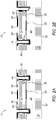
- Figs. 2-7 are schematic sectional views of enabled and disabled VCSELs. Each figure compares an enabled VCSEL (that can be used as the basis for enabled VCSELs 12), in a figure labeled by "a", to a disabled VCSEL (as a possible basis for dummy cells 16), in a figure labeled by "b". As the enabled and disabled VCSELs share most of the same elements, a detailed description of an enabled VCSEL is given with reference to Fig. 2a , below.
- Figs. 2a-b are schematic sectional views of an enabled VCSEL 17 and a disabled VCSEL 18, in accordance with an embodiment of the present invention.
- Enabled VCSEL 17 in Fig. 2a is formed on a semiconductor substrate 19.
- Epitaxial semiconductor layers of a VCSEL (a lower n-type distributed Bragg-reflector [n-DBR] stack 20, a quantum well structure 22, and an upper p-DBR stack 24) are deposited over an area of semiconductor substrate 19.
- a confinement layer 36 typically Al-oxide, is formed and patterned.
- an isolation layer 28 is deposited and patterned, and one or more p-electrodes 30 and n-electrodes 32 are deposited and patterned.
- Isolation trenches 34 are etched to define the array of VCSELs and to isolate neighboring VCSELs. Additionally, an isolation implant 38, such as a proton implant, may be deposited adjacent to p-DBR stack 24 and quantum well structure 22 for increased isolation between neighboring VCSELs.
- an isolation implant 38 such as a proton implant
- Disabled VCSEL 18 in Fig. 2b differs from enabled VCSEL 17 in that in the disabled VCSEL, isolation implant 38 extends into p-DBR stack 24 and possibly into quantum well structure 22. Due to the lattice damage caused by the ion implantation, the resistance of the implanted layers increases from the non-implanted state, lowering the excitation current injected into quantum well structure 22 to below the threshold required for emitting laser radiation. As a result, the VCSEL is disabled and will not emit laser radiation.
- Disabling of VCSEL 18 is achieved in the fabrication process by a modification of the photomask responsible for defining the lateral distribution of the deposition of isolation implant 38 so as to permit implantation ions to reach p-DBR stack 24 and possibly quantum well structure 22.
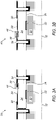
- Figs. 3a-b are schematic sectional views of an enabled VCSEL 39 and a disabled VCSEL 40, in accordance with another embodiment of the present invention.
- Enabled VCSEL 39 is substantially similar to enabled VCSEL 17 of Fig. 2a , except that the present embodiment does not necessarily comprise isolation implant 38 for isolating neighboring VCSELs.
- Disabling VCSEL 40 is accomplished by preventing the injection of excitation current into p-DBR stack 24 and quantum well structure 22.
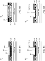
- the differences between enabled VCSEL 39 and disabled VCSEL 40 in three alternative embodiments of the present invention are shown in Figs. 4-6 . These figures refer to Figs. 3a-b , and show an area 44 (marked by a dotted line) for enabled VCSEL 39 and an area 46 (marked by a dotted line) for disabled VCSEL 40.
- Figs. 4a-b are schematic sectional views of areas 44 and 46 of enabled and disabled VCSELs 39 and 40 of Figs. 3a-b , respectively, in accordance with an embodiment of the present invention.
- an electrical contact between p-electrode 30 and p-DBR stack 24 is produced by etching a via in a location 41 in isolation layer 28 prior to deposition of the metal layer (M1) that serves as the p-electrode, thus enabling the flow of excitation current from the p-electrode to the p-DBR stack and further to quantum well structure 22.
- M1 metal layer
- disabled VCSEL 40 no via is etched, as is shown by contiguous isolation layer 28 in a location 42, thus preventing the flow of excitation current from p-electrode 30 into p-DBR stack 24 and further to quantum well structure 22.
- Disabling of VCSEL 40 is achieved in the fabrication process by a modification of the photomask responsible for delineating the etch of isolation layer 28 so as not to etch a via in location 42.
- Figs. 5a-b are schematic sectional views of areas 44 and 46 of enabled and disabled VCSELs 39 and 40 of Figs. 3a-b , respectively, in accordance with another embodiment of the present invention.
- a via is etched in isolation layer 28 in locations 62 and 64, respectively.
- a second isolation layer 60 is deposited over isolation layer 28, and a via is etched in enabled VCSEL 39 in location 62, whereas no via is etched in disabled VCSEL 40 in location 64.
- p-electrode 30 is deposited over second isolation layer 60, and the via etched in location 62 enables electrical contact between the p-electrode and p-DBR stack 24, thus enabling the flow of excitation current from the p-electrode to the p-DBR stack and further to quantum well structure 22.
- Disabling of VCSEL 40 is achieved in the fabrication process by a modification of the photomask responsible for delineating the etch of isolation layer 60 so as to prevent the etching of a via in location 64.
- Figs. 6a-b are schematic sectional views of areas 44 and 46 of enabled and disabled VCSELs 39 and 40 of Figs. 3a-b , respectively, in accordance with yet another embodiment of the present invention.
- an electrical contact between p-electrode 30 and p-DBR stack 24 is generated by etching a via in a location 41 in isolation layer 28, similarly to enabled VCSEL of Fig. 4a .
- a second isolation layer 66 is deposited over p-electrode 30 (as opposed to depositing over isolation layer 28, as in Figs. 5a-b ).
- a via is etched in second isolation layer 66 in a location 72, but no via is etched in a location 74.
- a conducting layer 76 is deposited on second isolation layer 66 for feeding electrical current to the array of optoelectronic cells.
- conducting layer 76 is in electrical contact with p-electrode 30, and thereby with p-DBR stack 24, enabling the flow of excitation current from the second metal layer to the p-DBR stack and further to quantum well structure 22.
- contiguous second isolation layer 66 in location 74 p-electrode 30 of disabled VCSEL 40 is isolated from conducting layer 76, thus preventing feeding of electrical current to the p-electrode.
- Disabling of VCSEL 40 is achieved in the fabrication process by a modification of the photomask responsible for delineating the etch of isolation layer 60 so as to prevent the etching of a via in location 74.
- Figs. 7a-b are schematic sectional views of an enabled VCSEL 80 and a disabled VCSEL 82, in accordance with an embodiment of the present invention.
- Enabled VCSEL 80 is substantially similar to enabled VCSEL 39 of Fig. 3a .
- Disabled VCSEL 82 differs from enabled VCSEL 80 in that confinement layer 36 is not etched in location 84, preventing the growth of quantum well structure 22.
- Disabling of VCSEL 80 is achieved in the fabrication process by a modification of the photomask so as to prevent the etch of confinement layer 36 in location 84.
Landscapes
- Physics & Mathematics (AREA)
- Condensed Matter Physics & Semiconductors (AREA)
- General Physics & Mathematics (AREA)
- Electromagnetism (AREA)
- Optics & Photonics (AREA)
- Geometry (AREA)
- Semiconductor Lasers (AREA)
Abstract
Description
- The present invention relates generally to optoelectronic devices, and particularly to devices configurable to emit patterned illumination.
- Existing and emerging consumer applications have created an increasing need for real-time three-dimensional (3D) imagers. These imaging devices, also commonly known as depth sensors or depth mappers, enable the remote measurement of distance (and often intensity) of each point on a target scene - so-called target scene depth - by illuminating the target scene with one or more optical beams and analyzing the reflected optical signal.
- Various methods are known in the art for generating light sources based on arrays of multiple light-emitting elements of optical radiation on a monolithic semiconductor substrate.
-
United States Patent Application Publication 2014/0211215 , whose disclosure is incorporated herein by reference, describes an optical apparatus, which includes a beam source configured to generate an optical beam having a pattern imposed thereon. In one embodiment, an optoelectronic device comprises a semiconductor die on which a monolithic array of vertical-cavity surface-emitting laser (VCSEL) diodes is formed in a two-dimensional pattern that is not a regular lattice. The term "regular lattice" means a two-dimensional pattern in which the spacing between adjacent elements in the pattern (for example, between adjacent emitters in a VCSEL array) is constant and is synonymous with a periodic lattice. The pattern can be uncorrelated, in the sense that the auto-correlation of the positions of the laser diodes as a function of transverse shift is insignificant for any shift larger than the diode size. Random, pseudo-random, and quasi-periodic patterns are examples of such uncorrelated patterns. - Embodiments of the present invention that are described hereinbelow provide improved methods for fabricating patterned light sources and light sources that can be produced by such methods.
- There is therefore provided, in accordance with an embodiment of the invention, an optoelectronic device, including a semiconductor substrate and an array of optoelectronic cells, which are formed on the semiconductor substrate. The cells include first epitaxial layers defining a lower distributed Bragg-reflector (DBR) stack; second epitaxial layers formed over the lower DBR stack, defining a quantum well structure; third epitaxial layers, formed over the quantum well structure, defining an upper DBR stack; and electrodes formed over the upper DBR stack, which are configurable to inject an excitation current into the quantum well structure of each optoelectronic cell. The array includes a first set of the optoelectronic cells that are configured to emit laser radiation in response to the excitation current and a second set of the optoelectronic cells, interleaved with the first set, in which at least one element of the optoelectronic cells, selected from among the epitaxial layers and the electrodes, is configured so that the optoelectronic cells in the second set do not emit the laser radiation.
- In a disclosed embodiment, the array is a regular array, while the first set of the optoelectronic cells are arranged in an uncorrelated pattern within the array.
- In one embodiment, the second set of the optoelectronic cells include implanted ions in the upper DBR stack, which increase an electrical resistance of the upper DBR stack by an amount sufficient to reduce the excitation current injected into the quantum well structure to below a threshold required for emitting laser radiation.
- In other embodiments, the electrodes of the second set of the optoelectronic cells are configured so as not to inject the excitation current into the quantum well structure. In one such embodiment, the optoelectronic cells include an isolation layer between the epitaxial layers and the electrodes, and a part of the isolation layer is etched away in the first set of the optoelectronic cells and is not etched in the second set of the optoelectronic cells, so that the excitation current is not injected into the quantum well structure of the second set of the optoelectronic cells. In another embodiment, the device includes conductors configured to feed electrical current to the optoelectronic cells, and an isolation layer, which isolates the electrodes of the second set of the optoelectronic cells from the conductors, so that the electrical current is not fed to the electrodes of the second set of the optoelectronic cells.
- Additionally or alternatively, the device includes an isolation layer formed between the lower and upper DBR stacks, wherein the isolation layer is etched out of an area of the quantum well structure in the first set of the optoelectronic cells and is not etched out of the second set of the optoelectronic cells.
- There is also provided, in accordance with an embodiment of the invention, a method for manufacturing an optoelectronic device. The method includes depositing first epitaxial layers on a semiconductor substrate to define a lower distributed Bragg-reflector (DBR) stack. Second epitaxial layers are deposited over the first epitaxial layers to define a quantum well structure. Third epitaxial layers are deposited over the second epitaxial layers to define an upper DBR stack. The epitaxial layers are etched to define an array of optoelectronic cells. Electrodes are deposited over the third epitaxial layers electrodes and are configurable to inject an excitation current into the quantum well structure of each optoelectronic cell so as to cause a first set of the optoelectronic cells to emit laser radiation in response to the excitation current. At least one element, selected from among the epitaxial layers and the electrodes, of a second set the optoelectronic cells, which is interleaved with the first set, is configured so that the optoelectronic cells in the second set do not emit the laser radiation.
- The present invention will be more fully understood from the following detailed description of the embodiments thereof, taken together with the drawings in which:
-
-
Fig. 1 is a schematic top view of an optoelectronic device comprising a semiconductor die on which a monolithic array of VCSELs has been formed in a two-dimensional pattern, in accordance with an embodiment of the present invention; -
Figs. 2a-b are schematic sectional views of an enabled VCSEL and a disabled VCSEL, in accordance with an embodiment of the present invention; -
Figs. 3a-b are schematic sectional views of an enabled VCSEL and a disabled VCSEL, in accordance with another embodiment of the present invention; -
Figs. 4a-b are schematic sectional views of areas of enabled and disabled VCSELs, in accordance with yet another embodiment of the present invention; -
Figs. 5a-b are schematic sectional views of areas of enabled and disabled VCSELs, in accordance with a further embodiment of the present invention; -
Figs. 6a-b are schematic sectional views of areas of enabled and disabled VCSELs, in accordance with still another embodiment of the present invention; and -
Figs. 7a-b are schematic sectional views of an enabled VCSEL and a disabled VCSEL, in accordance with an alternative embodiment of the present invention. - Light sources emitting multiple beams are used, inter alia, in 3-D (three-dimensional) mapping applications based on optical triangulation. As described in the above-mentioned
United States Patent Application Publication 2014/0211215 , it is advantageous to use a light source that projects a random or pseudo-random pattern on the target to be mapped. A desirable emitter for such a light source is a VCSEL (vertical-cavity surface-emitting laser) array, due to low power consumption, high reliability, and good beam quality. A random or pseudo-random pattern of emitters in a VCSEL array can be generated by a corresponding photolithographic mask. The non-periodic distribution of the emitters, however, may lead to reduced control over the photoresist pattern CD (critical dimensions), as well as poor etch uniformity due to uneven etch load effects. - The embodiments of the present invention that are described herein address the above limitations by fabricating a VCSEL array on a uniform grid, and disabling individual emitters. The disabled emitters can be interleaved with the enabled (operating) emitters in substantially any desired pattern, for example in a pseudo-random or otherwise uncorrelated pattern. The disclosed embodiments selectively disable emitters using modifications in the VCSEL fabrication process, for example by modifying the epitaxial layers or the electrodes of the VCSELs. As the design is based on a uniform grid, it can be manufactured reliably using standard photolithographic methods.
-
Fig. 1 is a schematic top view of an optoelectronic device comprising a semiconductor die 10 on which a monolithic array of enabledoptoelectronic cells 12, such as VCSELs, has been formed in an uncorrelated two-dimensional pattern, in accordance with an embodiment of the present invention. The array is formed on the semiconductor substrate by the same sort of photolithographic methods as are used to produce VCSEL arrays that are known in the art, with suitable thin film layer structures forming the VCSELs, and conductors providing electric power and ground connections fromcontact pads 14 toVCSELs 12 in the array. - The sort of uncorrelated pattern of enabled VCSELs 12 is produced using substantially the same processes as are used in fabricating a regular array (i.e., an array in the form of a regular lattice) of VCSEL-like cells. In contrast to a conventional regular array, however, only
VCSELs 12 are selectively enabled, while disabling the remaining VCSEL-like cells. These disabled cells are referred to herein as "dummy cells 16," since they are nearly identical in structure toVCSELs 12 but are incapable of laser emission due to thin film layer properties that are configured in the manufacturing process. In the following, the terms "disabling" and "disabled" are used synonymously with "not enabling" and "not enabled", respectively. - The ability to create an array of operating emitters in substantially any desired pattern, for example in a pseudo-random or otherwise uncorrelated pattern, based on a regular array of cells, has several advantages:
- an improved dry etch uniformity is achieved by minimizing so-called etch loading effects;
- a tighter control of photoresist CD is achieved due to the periodical structure of the uniform grid; and
- a more uniform temperature distribution of die 10 can be achieved, leading to a better optical power uniformity, by filling the trenches between cells with a resin, such as polyimide.
-
Figs. 2-7 are schematic sectional views of enabled and disabled VCSELs. Each figure compares an enabled VCSEL (that can be used as the basis for enabled VCSELs 12), in a figure labeled by "a", to a disabled VCSEL (as a possible basis for dummy cells 16), in a figure labeled by "b". As the enabled and disabled VCSELs share most of the same elements, a detailed description of an enabled VCSEL is given with reference toFig. 2a , below. -
Figs. 2a-b are schematic sectional views of an enabledVCSEL 17 and adisabled VCSEL 18, in accordance with an embodiment of the present invention. - Enabled
VCSEL 17 inFig. 2a is formed on asemiconductor substrate 19. Epitaxial semiconductor layers of a VCSEL (a lower n-type distributed Bragg-reflector [n-DBR]stack 20, aquantum well structure 22, and an upper p-DBR stack 24) are deposited over an area ofsemiconductor substrate 19. Between n-DBR stack 20 and p-DBR stack 24 aconfinement layer 36, typically Al-oxide, is formed and patterned. Following the deposition of p-DBR stack 24, anisolation layer 28 is deposited and patterned, and one or more p-electrodes 30 and n-electrodes 32 are deposited and patterned.Isolation trenches 34 are etched to define the array of VCSELs and to isolate neighboring VCSELs. Additionally, anisolation implant 38, such as a proton implant, may be deposited adjacent to p-DBR stack 24 andquantum well structure 22 for increased isolation between neighboring VCSELs. -
Disabled VCSEL 18 inFig. 2b differs from enabledVCSEL 17 in that in the disabled VCSEL,isolation implant 38 extends into p-DBR stack 24 and possibly intoquantum well structure 22. Due to the lattice damage caused by the ion implantation, the resistance of the implanted layers increases from the non-implanted state, lowering the excitation current injected intoquantum well structure 22 to below the threshold required for emitting laser radiation. As a result, the VCSEL is disabled and will not emit laser radiation. - Disabling of
VCSEL 18 is achieved in the fabrication process by a modification of the photomask responsible for defining the lateral distribution of the deposition ofisolation implant 38 so as to permit implantation ions to reach p-DBR stack 24 and possiblyquantum well structure 22. -
Figs. 3a-b are schematic sectional views of an enabledVCSEL 39 and adisabled VCSEL 40, in accordance with another embodiment of the present invention. EnabledVCSEL 39 is substantially similar to enabledVCSEL 17 ofFig. 2a , except that the present embodiment does not necessarily compriseisolation implant 38 for isolating neighboring VCSELs. DisablingVCSEL 40 is accomplished by preventing the injection of excitation current into p-DBR stack 24 andquantum well structure 22. The differences between enabledVCSEL 39 anddisabled VCSEL 40 in three alternative embodiments of the present invention are shown inFigs. 4-6 . These figures refer toFigs. 3a-b , and show an area 44 (marked by a dotted line) for enabledVCSEL 39 and an area 46 (marked by a dotted line) fordisabled VCSEL 40. -
Figs. 4a-b are schematic sectional views ofareas disabled VCSELs Figs. 3a-b , respectively, in accordance with an embodiment of the present invention. - In enabled
VCSEL 39 an electrical contact between p-electrode 30 and p-DBR stack 24 is produced by etching a via in alocation 41 inisolation layer 28 prior to deposition of the metal layer (M1) that serves as the p-electrode, thus enabling the flow of excitation current from the p-electrode to the p-DBR stack and further toquantum well structure 22. Indisabled VCSEL 40 no via is etched, as is shown bycontiguous isolation layer 28 in alocation 42, thus preventing the flow of excitation current from p-electrode 30 into p-DBR stack 24 and further toquantum well structure 22. - Disabling of
VCSEL 40 is achieved in the fabrication process by a modification of the photomask responsible for delineating the etch ofisolation layer 28 so as not to etch a via inlocation 42. -
Figs. 5a-b are schematic sectional views ofareas disabled VCSELs Figs. 3a-b , respectively, in accordance with another embodiment of the present invention. - In both enabled
VCSEL 39 and disabled VCSEL 40 a via is etched inisolation layer 28 inlocations second isolation layer 60 is deposited overisolation layer 28, and a via is etched in enabledVCSEL 39 inlocation 62, whereas no via is etched indisabled VCSEL 40 inlocation 64. p-electrode 30 is deposited oversecond isolation layer 60, and the via etched inlocation 62 enables electrical contact between the p-electrode and p-DBR stack 24, thus enabling the flow of excitation current from the p-electrode to the p-DBR stack and further toquantum well structure 22. However, no electrical contact is established between p-electrode 30 and p-DBR stack 24 ofdisabled VCSEL 40 due to contiguoussecond isolation layer 60 inlocation 64, thus preventing the flow of excitation current from the p-electrode into the p-DBR stack and further toquantum well structure 22. - Disabling of
VCSEL 40 is achieved in the fabrication process by a modification of the photomask responsible for delineating the etch ofisolation layer 60 so as to prevent the etching of a via inlocation 64. -
Figs. 6a-b are schematic sectional views ofareas disabled VCSELs Figs. 3a-b , respectively, in accordance with yet another embodiment of the present invention. - In both enabled
VCSEL 39 anddisabled VCSEL 40 an electrical contact between p-electrode 30 and p-DBR stack 24 is generated by etching a via in alocation 41 inisolation layer 28, similarly to enabled VCSEL ofFig. 4a . Asecond isolation layer 66 is deposited over p-electrode 30 (as opposed to depositing overisolation layer 28, as inFigs. 5a-b ). A via is etched insecond isolation layer 66 in alocation 72, but no via is etched in alocation 74. A conductinglayer 76 is deposited onsecond isolation layer 66 for feeding electrical current to the array of optoelectronic cells. Due to the via etched inlocation 72, conductinglayer 76 is in electrical contact with p-electrode 30, and thereby with p-DBR stack 24, enabling the flow of excitation current from the second metal layer to the p-DBR stack and further toquantum well structure 22. However, due to contiguoussecond isolation layer 66 inlocation 74, p-electrode 30 ofdisabled VCSEL 40 is isolated from conductinglayer 76, thus preventing feeding of electrical current to the p-electrode. - Disabling of
VCSEL 40 is achieved in the fabrication process by a modification of the photomask responsible for delineating the etch ofisolation layer 60 so as to prevent the etching of a via inlocation 74. -
Figs. 7a-b are schematic sectional views of an enabledVCSEL 80 and adisabled VCSEL 82, in accordance with an embodiment of the present invention. EnabledVCSEL 80 is substantially similar to enabledVCSEL 39 ofFig. 3a .Disabled VCSEL 82 differs from enabledVCSEL 80 in thatconfinement layer 36 is not etched inlocation 84, preventing the growth ofquantum well structure 22. - Disabling of
VCSEL 80 is achieved in the fabrication process by a modification of the photomask so as to prevent the etch ofconfinement layer 36 inlocation 84. - It will be appreciated that the embodiments described above are cited by way of example, and that the present invention is not limited to what has been particularly shown and described hereinabove. Rather, the scope of the present invention includes both combinations and subcombinations of the various features described hereinabove, as well as variations and modifications thereof which would occur to persons skilled in the art upon reading the foregoing description and which are not disclosed in the prior art.
-
- 1. An optoelectronic device, comprising:
- a semiconductor substrate; and
- an array of optoelectronic cells, which are formed on the semiconductor substrate and comprise:
- first epitaxial layers defining a lower distributed Bragg-reflector (DBR) stack;
- second epitaxial layers formed over the lower DBR stack, defining a quantum well structure;
- third epitaxial layers, formed over the quantum well structure, defining an upper DBR stack; and
- electrodes formed over the upper DBR stack, which are configurable to inject an excitation current into the quantum well structure of each optoelectronic cell,
- wherein the array comprises a first set of the optoelectronic cells that are configured to emit laser radiation in response to the excitation current and a second set of the optoelectronic cells, interleaved with the first set, in which at least one element of the optoelectronic cells, selected from among the epitaxial layers and the electrodes, is configured so that the optoelectronic cells in the second set do not emit the laser radiation.
- 2. The optoelectronic device of
statement 1, wherein the array is a regular array, while the first set of the optoelectronic cells are arranged in an uncorrelated pattern within the array. - 3. The optoelectronic device of
statement - 4. The optoelectronic device of
statement - 5. The optoelectronic device of statement 4, wherein the optoelectronic cells comprise an isolation layer between the epitaxial layers and the electrodes, and wherein a part of the isolation layer is etched away in the first set of the optoelectronic cells and is not etched in the second set of the optoelectronic cells, so that the excitation current is not injected into the quantum well structure of the second set of the optoelectronic cells.
- 6. The optoelectronic device of statement 4, and comprising conductors configured to feed electrical current to the optoelectronic cells, and an isolation layer, which isolates the electrodes of the second set of the optoelectronic cells from the conductors, so that the electrical current is not fed to the electrodes of the second set of the optoelectronic cells.
- 7. The optoelectronic device of
statement - 8. A method for manufacturing an optoelectronic device, the method comprising:
- depositing first epitaxial layers on a semiconductor substrate to define a lower distributed Bragg-reflector (DBR) stack;
- depositing second epitaxial layers over the first epitaxial layers to define a quantum well structure;
- depositing third epitaxial layers over the second epitaxial layers to define an upper DBR stack;
- etching the epitaxial layers to define an array of optoelectronic cells;
- depositing over the third epitaxial layers electrodes configurable to inject an excitation current into the quantum well structure of each optoelectronic cell so as to cause a first set of the optoelectronic cells to emit laser radiation in response to the excitation current; and
- configuring at least one element, selected from among the epitaxial layers and the electrodes, of a second set the optoelectronic cells, which is interleaved with the first set, so that the optoelectronic cells in the second set do not emit the laser radiation.
- 9. The method of statement 8, wherein the array is a regular array, while the first set of the optoelectronic cells are arranged in an uncorrelated pattern within the array.
- 10. The method of statement 8 or 9, wherein configuring the at least one element comprises implanting ions in the upper DBR stack, which increase the electrical resistance of the upper DBR stack by an amount sufficient to reduce the excitation current injected into the quantum well structure to below a threshold required for emitting laser radiation.
- 11. The method of statement 8 or 9, wherein configuring the at least one element comprises configuring the electrodes of the second set not to inject the excitation current into the quantum well structure.
- 12. The method of statement 11, wherein configuring the electrodes comprises forming an isolation layer between epitaxial layers and the electrodes, and etching away a part of the isolation layer in the first set of the optoelectronic cells while not etching the isolation layer in the second set of the optoelectronic cells, so that the excitation current is not injected into the quantum well structure of the second set of the optoelectronic cells.
- 13. The method of statement 11, wherein configuring the electrodes comprises configuring conductors to feed electrical current to the array of optoelectronic cells, and depositing and patterning an isolation layer so as to isolate the electrodes of the second set of the optoelectronic cells from the conductors, so that the electrical current is not fed to the electrodes of the second set of the optoelectronic cells.
- 14. The method of statement 8 or 9, wherein configuring the at least one element comprises depositing an isolation layer between the lower and upper DBR stacks and etching the isolation layer out of an area of the quantum well structure in the first set of the optoelectronic cells while not etching the isolation layer out of the second set of the optoelectronic cells.
Claims (10)
- An optoelectronic device (10), comprising:a semiconductor substrate; andan array of optoelectronic cells (12, 16), which are formed on the semiconductor substrate and comprise:first epitaxial layers (20) defining a lower distributed Bragg-reflector, DBR, stack;second epitaxial layers (22) formed over the lower DBR stack, defining a quantum well structure;third epitaxial layers (24), formed over the quantum well structure, defining an upper DBR stack; andelectrodes (30) formed over the upper DBR stack, which are configurable to inject an excitation current into the quantum well structure of each optoelectronic cell,wherein the array comprises a first set of the optoelectronic cells (12) that are configured to emit laser radiation in response to the excitation current and a second set of the optoelectronic cells (16), interleaved with the first set, in which the electrodes are configured so as not to inject the excitation current into the quantum well structure,whereby the optoelectronic cells in the second set do not emit the laser radiation.
- The optoelectronic device of claim 1, wherein the array is a regular array, while the first set of the optoelectronic cells are arranged in an uncorrelated pattern within the array.
- The optoelectronic device of claim 1 or 2, wherein the optoelectronic cells comprise an isolation layer between the epitaxial layers and the electrodes, and wherein a part of the isolation layer is etched away in the first set of the optoelectronic cells and is not etched in the second set of the optoelectronic cells, so that the excitation current is not injected into the quantum well structure of the second set of the optoelectronic cells.
- The optoelectronic device of claim 1 or 2, and comprising conductors configured to feed electrical current to the optoelectronic cells, and an isolation layer, which isolates the electrodes of the second set of the optoelectronic cells from the conductors, so that the electrical current is not fed to the electrodes of the second set of the optoelectronic cells.
- An optoelectronic device (10), comprising:a semiconductor substrate (19); andan array of optoelectronic cells (12, 16), which are formed on the semiconductor substrate and comprise:first epitaxial layers (20) defining a lower distributed Bragg-reflector, DBR, stack;second epitaxial layers (22) formed over the lower DBR stack, defining a quantum well structure;third epitaxial layers (24), formed over the quantum well structure, defining an upper DBR stack; andelectrodes (30) formed over the upper DBR stack, which are configurable to inject an excitation current into the quantum well structure of each optoelectronic cell,wherein the array comprises a first set of the optoelectronic cells that are configured to emit laser radiation in response to the excitation current and a second set of the optoelectronic cells, interleaved with the first set, in which ions are implanted in the upper DBR stack so as to increase an electrical resistance of the upper DBR stack by an amount sufficient to reduce the excitation current injected into the quantum well structure to below a threshold required for emitting laser radiation, whereby the optoelectronic cells in the second set do not emit the laser radiation.
- The optoelectronic device of claim 5, wherein the array is a regular array, while the first set of the optoelectronic cells are arranged in an uncorrelated pattern within the array.
- A method for manufacturing an optoelectronic device (10), the method comprising:depositing first epitaxial layers (20) on a semiconductor substrate (19) to define a lower distributed Bragg-reflector, DBR, stack;depositing second epitaxial layers (22) over the first epitaxial layers to define a quantum well structure;depositing third epitaxial layers (24) over the second epitaxial layers to define an upper DBR stack;etching the epitaxial layers to define an array of optoelectronic cells (12, 16);depositing over the third epitaxial layers electrodes (30) configured to inject an excitation current into the quantum well structure of at least some of the optoelectronic cells so as to cause a first set of the optoelectronic cells (12) to emit laser radiation in response to the excitation current; andconfiguring the electrodes of a second set the optoelectronic cells, which is interleaved with the first set, so as not to inject the excitation current into the quantum well structure of the optoelectronic cells in the second set (16), whereby the optoelectronic cells in the second set do not emit the laser radiation.
- The method of claim 7, wherein the array is a regular array, while the first set of the optoelectronic cells are arranged in an uncorrelated pattern within the array.
- The method of claim 7 or 8, wherein configuring the electrodes comprises forming an isolation layer between epitaxial layers and the electrodes, and etching away a part of the isolation layer in the first set of the optoelectronic cells while not etching the isolation layer in the second set of the optoelectronic cells, so that the excitation current is not injected into the quantum well structure of the second set of the optoelectronic cells.
- The method of claim 7 or 8, wherein configuring the electrodes comprises configuring conductors to feed electrical current to the array of optoelectronic cells, and depositing and patterning an isolation layer so as to isolate the electrodes of the second set of the optoelectronic cells from the conductors, so that the electrical current is not fed to the electrodes of the second set of the optoelectronic cells.
Applications Claiming Priority (4)
| Application Number | Priority Date | Filing Date | Title |
|---|---|---|---|
| US201762552406P | 2017-08-31 | 2017-08-31 | |
| US15/844,662 US10153614B1 (en) | 2017-08-31 | 2017-12-18 | Creating arbitrary patterns on a 2-D uniform grid VCSEL array |
| PCT/US2018/040531 WO2019045873A1 (en) | 2017-08-31 | 2018-07-02 | Creating arbitrary patterns on a 2-d uniform grid vcsel array |
| EP18743354.5A EP3656028B1 (en) | 2017-08-31 | 2018-07-02 | Creating arbitrary patterns on a 2-d uniform grid vcsel array |
Related Parent Applications (2)
| Application Number | Title | Priority Date | Filing Date |
|---|---|---|---|
| EP18743354.5A Division-Into EP3656028B1 (en) | 2017-08-31 | 2018-07-02 | Creating arbitrary patterns on a 2-d uniform grid vcsel array |
| EP18743354.5A Division EP3656028B1 (en) | 2017-08-31 | 2018-07-02 | Creating arbitrary patterns on a 2-d uniform grid vcsel array |
Publications (2)
| Publication Number | Publication Date |
|---|---|
| EP4047762A1 true EP4047762A1 (en) | 2022-08-24 |
| EP4047762B1 EP4047762B1 (en) | 2024-10-23 |
Family
ID=64535818
Family Applications (2)
| Application Number | Title | Priority Date | Filing Date |
|---|---|---|---|
| EP18743354.5A Active EP3656028B1 (en) | 2017-08-31 | 2018-07-02 | Creating arbitrary patterns on a 2-d uniform grid vcsel array |
| EP22159829.5A Active EP4047762B1 (en) | 2017-08-31 | 2018-07-02 | Creating arbitrary patterns on a 2-d uniform grid vcsel array |
Family Applications Before (1)
| Application Number | Title | Priority Date | Filing Date |
|---|---|---|---|
| EP18743354.5A Active EP3656028B1 (en) | 2017-08-31 | 2018-07-02 | Creating arbitrary patterns on a 2-d uniform grid vcsel array |
Country Status (7)
| Country | Link |
|---|---|
| US (4) | US10153614B1 (en) |
| EP (2) | EP3656028B1 (en) |
| JP (2) | JP6931419B2 (en) |
| KR (2) | KR102351103B1 (en) |
| CN (2) | CN109428261B (en) |
| TW (3) | TWI720744B (en) |
| WO (1) | WO2019045873A1 (en) |
Families Citing this family (17)
| Publication number | Priority date | Publication date | Assignee | Title |
|---|---|---|---|---|
| US10153614B1 (en) * | 2017-08-31 | 2018-12-11 | Apple Inc. | Creating arbitrary patterns on a 2-D uniform grid VCSEL array |
| US10666020B2 (en) * | 2017-09-20 | 2020-05-26 | Lumentum Operations Llc | Reconfigurable emitter array |
| US11594860B2 (en) * | 2017-11-20 | 2023-02-28 | Ii-Vi Delaware, Inc. | VCSEL array layout |
| US20190237940A1 (en) | 2018-01-26 | 2019-08-01 | Lumentum Operations Llc | Modified emitter array |
| CN108923261B (en) * | 2018-10-24 | 2019-01-29 | 常州纵慧芯光半导体科技有限公司 | Dot structure of vertical cavity surface emitting laser and preparation method thereof |
| US11549799B2 (en) * | 2019-07-01 | 2023-01-10 | Apple Inc. | Self-mixing interference device for sensing applications |
| DE112021000652T5 (en) * | 2020-01-20 | 2022-11-24 | Hamamatsu Photonics K.K. | light source module |
| JP6891327B1 (en) * | 2020-09-25 | 2021-06-18 | 浜松ホトニクス株式会社 | Light source module |
| JP7308157B2 (en) * | 2020-01-20 | 2023-07-13 | 浜松ホトニクス株式会社 | light source module |
| CN114175428B (en) * | 2020-02-24 | 2024-10-11 | 深圳瑞识智能科技有限公司 | VCSEL arrays with non-isolated emitters |
| US12586986B2 (en) * | 2020-06-25 | 2026-03-24 | Sony Group Corporation | Light-emitting device |
| WO2023019384A1 (en) * | 2021-08-16 | 2023-02-23 | Shenzhen Raysees AI Technology Co., Ltd. | Vcsel array with different emitter structures |
| US12413043B2 (en) | 2021-09-21 | 2025-09-09 | Apple Inc. | Self-mixing interference device with tunable microelectromechanical system |
| CN114188816B (en) * | 2021-11-16 | 2024-04-12 | 深圳市嘉敏利光电有限公司 | Flip VCSEL structure of high refractive index contrast DBR and process method thereof |
| CN116845694A (en) * | 2022-03-23 | 2023-10-03 | 浙江睿熙科技有限公司 | Flow-controlled balanced VCSEL chip and preparation method thereof |
| US12613131B2 (en) | 2022-09-22 | 2026-04-28 | Apple Inc. | Optical proximity sensor |
| US12601583B2 (en) | 2023-05-17 | 2026-04-14 | Apple Inc. | Multi-channel self-mixing interferometric sensor |
Citations (6)
| Publication number | Priority date | Publication date | Assignee | Title |
|---|---|---|---|---|
| JP2000114656A (en) * | 1998-10-05 | 2000-04-21 | Fuji Xerox Co Ltd | Surface-emission laser array apparatus |
| JP2011003748A (en) * | 2009-06-19 | 2011-01-06 | Fuji Xerox Co Ltd | Surface emitting semiconductor laser, surface emitting semiconductor laser device, optical transmission device, and information processing device |
| JP2014135371A (en) * | 2013-01-10 | 2014-07-24 | Ricoh Co Ltd | Surface emitting laser, surface emitting laser array and optical scanning device |
| US20140211215A1 (en) | 2011-08-09 | 2014-07-31 | Primesense Ltd. | Projectors of structured light |
| US20160072258A1 (en) * | 2014-09-10 | 2016-03-10 | Princeton Optronics Inc. | High Resolution Structured Light Source |
| US20160164261A1 (en) * | 2009-02-17 | 2016-06-09 | Trilumina Corp. | Compact multi-zone infrared laser illuminator |
Family Cites Families (113)
| Publication number | Priority date | Publication date | Assignee | Title |
|---|---|---|---|---|
| JPS5243095B2 (en) | 1973-08-03 | 1977-10-28 | ||
| US4390234A (en) | 1980-08-14 | 1983-06-28 | Embach James T | Viewer/projector for display of 360 degree holographic film cassettes |
| DE3212809C2 (en) | 1982-04-06 | 1984-12-20 | Fa. Carl Zeiss, 7920 Heidenheim | Measuring device for the stabilization of lasers |
| US5082339A (en) | 1988-07-11 | 1992-01-21 | Telefunken Electronic Gmbh | Optical read-write head with diffraction grating structure |
| EP0452793B1 (en) | 1990-04-12 | 1998-01-28 | Matsushita Electric Industrial Co., Ltd. | Optical head having a hologram associated with the objective lens |
| US6732929B2 (en) | 1990-09-10 | 2004-05-11 | Metrologic Instruments, Inc. | Led-based planar light illumination beam generation module employing a focal lens for reducing the image size of the light emmiting surface of the led prior to beam collimation and planarization |
| US5325386A (en) * | 1992-04-21 | 1994-06-28 | Bandgap Technology Corporation | Vertical-cavity surface emitting laser assay display system |
| US5477383A (en) * | 1993-02-05 | 1995-12-19 | Apa Optics, Inc. | Optical array method and apparatus |
| JP3537881B2 (en) | 1994-03-29 | 2004-06-14 | 株式会社リコー | LED array head |
| JPH08328511A (en) * | 1995-03-30 | 1996-12-13 | Toshiba Corp | LED display device and display control method thereof |
| US5809053A (en) | 1995-07-05 | 1998-09-15 | Hitachi, Ltd. | Semiconductor laser device and optical printing apparatus using the same |
| US6144685A (en) | 1996-01-23 | 2000-11-07 | Fuji Xerox Co., Ltd. | Two-dimensional surface emitting laser array, two-dimensional surface emitting laser beam scanner, two-dimensional surface emitting laser beam recorder, and two-dimensional surface emitting laser beam recording method |
| JP3631551B2 (en) | 1996-01-23 | 2005-03-23 | 株式会社ミツトヨ | Optical encoder |
| US5784396A (en) * | 1996-09-17 | 1998-07-21 | Xerox Corporation | VCSEL integral feedback assembly two-etch structure |
| JPH10254370A (en) | 1997-03-10 | 1998-09-25 | Canon Inc | Display panel and projection display device using the same |
| US6243407B1 (en) | 1997-03-21 | 2001-06-05 | Novalux, Inc. | High power laser devices |
| US7028899B2 (en) | 1999-06-07 | 2006-04-18 | Metrologic Instruments, Inc. | Method of speckle-noise pattern reduction and apparatus therefore based on reducing the temporal-coherence of the planar laser illumination beam before it illuminates the target object by applying temporal phase modulation techniques during the transmission of the plib towards the target |
| JPH11168262A (en) * | 1997-09-30 | 1999-06-22 | Canon Inc | Surface type optical device, manufacturing method thereof, and display device |
| US6026110A (en) * | 1997-10-16 | 2000-02-15 | Nortel Networks Corporation | Distributed feedback semiconductor laser with gain modulation |
| US6061485A (en) | 1997-11-03 | 2000-05-09 | Motorola, Inc. | Method for wavelength division multiplexing utilizing donut mode vertical cavity surface emitting lasers |
| US6002705A (en) * | 1997-12-03 | 1999-12-14 | Xerox Corporation | Wavelength and polarization multiplexed vertical cavity surface emitting lasers |
| US6084900A (en) | 1997-12-24 | 2000-07-04 | Motorola, Inc. | Annular waveguide vertical cavity surface emitting laser array and method of fabrication |
| US6597713B2 (en) | 1998-07-22 | 2003-07-22 | Canon Kabushiki Kaisha | Apparatus with an optical functional device having a special wiring electrode and method for fabricating the same |
| US6636538B1 (en) | 1999-03-29 | 2003-10-21 | Cutting Edge Optronics, Inc. | Laser diode packaging |
| EP1067362A1 (en) | 1999-07-09 | 2001-01-10 | Hewlett-Packard Company | Document imaging system |
| US6888871B1 (en) | 2000-07-12 | 2005-05-03 | Princeton Optronics, Inc. | VCSEL and VCSEL array having integrated microlenses for use in a semiconductor laser pumped solid state laser system |
| WO2002037410A1 (en) | 2000-11-06 | 2002-05-10 | Koninklijke Philips Electronics N.V. | Method of measuring the movement of an input device. |
| US6734981B1 (en) | 2000-11-28 | 2004-05-11 | Honeywell International Inc. | Multiple laser optical systems and methods |
| DE10111871A1 (en) * | 2001-03-13 | 2002-09-19 | Heidelberger Druckmasch Ag | Imaging device for a printing form with an array of VCSEL light sources |
| US6611000B2 (en) * | 2001-03-14 | 2003-08-26 | Matsushita Electric Industrial Co., Ltd. | Lighting device |
| US6639177B2 (en) | 2001-03-29 | 2003-10-28 | Gsi Lumonics Corporation | Method and system for processing one or more microstructures of a multi-material device |
| WO2002089221A1 (en) | 2001-04-23 | 2002-11-07 | Matsushita Electric Works, Ltd. | Light emitting device comprising led chip |
| US6680963B2 (en) | 2001-07-24 | 2004-01-20 | Lux Net Corporation | Vertical-cavity surface emitting laser utilizing a reversed biased diode for improved current confinement |
| EP2009676B8 (en) | 2002-05-08 | 2012-11-21 | Phoseon Technology, Inc. | A semiconductor materials inspection system |
| US7279069B2 (en) | 2002-07-18 | 2007-10-09 | Origin Electric Company Limited | Adhesive curing method, curing apparatus, and optical disc lamination apparatus using the curing apparatus |
| KR100624405B1 (en) | 2002-10-01 | 2006-09-18 | 삼성전자주식회사 | Optical component mounting board and its manufacturing method |
| US6853660B2 (en) * | 2002-10-16 | 2005-02-08 | Eastman Kodak Company | Organic laser cavity arrays |
| US7257141B2 (en) * | 2003-07-23 | 2007-08-14 | Palo Alto Research Center Incorporated | Phase array oxide-confined VCSELs |
| US7164702B1 (en) | 2003-08-29 | 2007-01-16 | The United States Of America As Represented By The Secretary Of The Army | Optical transmitters and interconnects using surface-emitting lasers and micro-optical elements |
| US8009358B2 (en) | 2003-10-17 | 2011-08-30 | Explay Ltd. | Optical system and method for use in projection systems |
| KR20070018805A (en) | 2003-10-17 | 2007-02-14 | 익스플레이 엘티디. | Optical system and method for use in projection systems |
| DE602004030376D1 (en) | 2003-12-22 | 2011-01-13 | Panasonic Corp | SURFACE EMISSIONS LASER AND LASER PROJECTOR |
| JP4572312B2 (en) | 2004-02-23 | 2010-11-04 | スタンレー電気株式会社 | LED and manufacturing method thereof |
| WO2005111693A1 (en) | 2004-05-17 | 2005-11-24 | Olympus Corporation | Head-mounted type image display device |
| JP5128047B2 (en) | 2004-10-07 | 2013-01-23 | Towa株式会社 | Optical device and optical device production method |
| IL165212A (en) | 2004-11-15 | 2012-05-31 | Elbit Systems Electro Optics Elop Ltd | Device for scanning light |
| US7750356B2 (en) | 2005-05-04 | 2010-07-06 | Avago Technologies Fiber Ip (Singapore) Pte. Ltd. | Silicon optical package with 45 degree turning mirror |
| JP2007105205A (en) | 2005-10-13 | 2007-04-26 | Erecta International Corp | Control method and rice cooking method of catering unit |
| US8018579B1 (en) | 2005-10-21 | 2011-09-13 | Apple Inc. | Three-dimensional imaging and display system |
| US8792978B2 (en) | 2010-05-28 | 2014-07-29 | Lockheed Martin Corporation | Laser-based nerve stimulators for, E.G., hearing restoration in cochlear prostheses and method |
| KR101408959B1 (en) | 2006-03-14 | 2014-07-02 | 프라임센스 엘티디. | Depth-varying light fields for three dimensional sensing |
| JP2008109083A (en) | 2006-09-29 | 2008-05-08 | Seiko Epson Corp | Laser light source device, illumination device, monitor device, and projector |
| US20080144183A1 (en) | 2006-12-18 | 2008-06-19 | Motorola, Inc. | Compact three color laser system with light intensity sensor |
| JP2008244431A (en) * | 2007-02-28 | 2008-10-09 | Canon Inc | Surface emitting laser array, method of manufacturing the same, and image forming apparatus including surface emitting laser array |
| WO2008108468A1 (en) | 2007-03-08 | 2008-09-12 | Rohm Co., Ltd. | Led illumination device and its drive method |
| JP5029079B2 (en) | 2007-03-15 | 2012-09-19 | 富士ゼロックス株式会社 | Semiconductor element and optical device |
| US8150142B2 (en) | 2007-04-02 | 2012-04-03 | Prime Sense Ltd. | Depth mapping using projected patterns |
| WO2008120217A2 (en) | 2007-04-02 | 2008-10-09 | Prime Sense Ltd. | Depth mapping using projected patterns |
| JP5228363B2 (en) | 2007-04-18 | 2013-07-03 | ソニー株式会社 | Light emitting element |
| JP5183111B2 (en) * | 2007-07-05 | 2013-04-17 | キヤノン株式会社 | Vertical cavity surface emitting laser array and image forming apparatus using vertical cavity surface emitting laser array |
| KR101439434B1 (en) | 2007-10-05 | 2014-09-12 | 삼성전자주식회사 | Image sensor and manufacturing method thereof |
| US8384997B2 (en) | 2008-01-21 | 2013-02-26 | Primesense Ltd | Optical pattern projection |
| EP2235584B1 (en) | 2008-01-21 | 2020-09-16 | Apple Inc. | Optical designs for zero order reduction |
| EP2250818A1 (en) | 2008-02-08 | 2010-11-17 | Koninklijke Philips Electronics N.V. | Light module device |
| JP5171318B2 (en) * | 2008-03-05 | 2013-03-27 | キヤノン株式会社 | Surface emitting laser array |
| US7821649B2 (en) | 2008-03-05 | 2010-10-26 | Ge Inspection Technologies, Lp | Fringe projection system and method for a probe suitable for phase-shift analysis |
| FR2932562B1 (en) | 2008-06-12 | 2010-08-27 | Univ Pasteur | LIGHT PROJECTION DEVICE STRUCTURED BY MEANS OF VCSEL AND PHASE DIFFRACTIVE OPTICAL COMPONENTS. |
| US8456517B2 (en) | 2008-07-09 | 2013-06-04 | Primesense Ltd. | Integrated processor for 3D mapping |
| EP2311092B1 (en) | 2008-07-25 | 2021-01-27 | Cornell University | Light field image sensor, method and applications |
| JP5446635B2 (en) | 2008-09-16 | 2014-03-19 | 株式会社リコー | Image forming apparatus and image forming method |
| US8717416B2 (en) | 2008-09-30 | 2014-05-06 | Texas Instruments Incorporated | 3D camera using flash with structured light |
| US8107147B2 (en) | 2009-03-27 | 2012-01-31 | Microvision, Inc. | Two-mirror scanning system |
| US8287386B2 (en) * | 2009-06-08 | 2012-10-16 | Cfph, Llc | Electrical transmission among interconnected gaming systems |
| KR101733422B1 (en) | 2009-08-20 | 2017-05-10 | 코닌클리케 필립스 엔.브이. | Laser device with configurable intensity distribution |
| JP5588310B2 (en) | 2009-11-15 | 2014-09-10 | プライムセンス リミテッド | Optical projector with beam monitor |
| US8320621B2 (en) | 2009-12-21 | 2012-11-27 | Microsoft Corporation | Depth projector system with integrated VCSEL array |
| US20110188054A1 (en) | 2010-02-02 | 2011-08-04 | Primesense Ltd | Integrated photonics module for optical projection |
| US20110187878A1 (en) | 2010-02-02 | 2011-08-04 | Primesense Ltd. | Synchronization of projected illumination with rolling shutter of image sensor |
| JP5626559B2 (en) | 2010-02-09 | 2014-11-19 | アイシン精機株式会社 | Defect determination apparatus and defect determination method |
| DE102010012604A1 (en) | 2010-03-24 | 2011-09-29 | Osram Opto Semiconductors Gmbh | Semiconductor laser light source |
| JP2011228553A (en) | 2010-04-21 | 2011-11-10 | Hamamatsu Photonics Kk | Semiconductor light-emitting element array |
| US8330804B2 (en) | 2010-05-12 | 2012-12-11 | Microsoft Corporation | Scanned-beam depth mapping to 2D image |
| US8654152B2 (en) | 2010-06-21 | 2014-02-18 | Microsoft Corporation | Compartmentalizing focus area within field of view |
| JP5605042B2 (en) | 2010-07-15 | 2014-10-15 | 株式会社リコー | Semiconductor laser driving device and image forming apparatus provided with the driving device |
| WO2012020380A1 (en) | 2010-08-11 | 2012-02-16 | Primesense Ltd. | Scanning projectors and image capture modules for 3d mapping |
| WO2012027410A1 (en) | 2010-08-23 | 2012-03-01 | Lighttime, Llc | Ladar using mems scanning |
| US9620934B2 (en) | 2010-08-31 | 2017-04-11 | Avago Technologies General Ip (Singapore) Pte. Ltd. | Flip-chip assembly comprising an array of vertical cavity surface emitting lasers (VCSELs) |
| EP2643659B1 (en) | 2010-11-19 | 2019-12-25 | Apple Inc. | Depth mapping using time-coded illumination |
| JP2012122844A (en) | 2010-12-08 | 2012-06-28 | Aisin Seiki Co Ltd | Surface inspection device |
| US9052512B2 (en) | 2011-03-03 | 2015-06-09 | Asahi Glass Company, Limited | Diffractive optical element and measuring apparatus |
| JP2012195434A (en) | 2011-03-16 | 2012-10-11 | Ricoh Co Ltd | Surface light emitting laser module, optical scanner using surface light emitting laser module, and image formation device |
| JP5698578B2 (en) | 2011-03-24 | 2015-04-08 | オリンパス株式会社 | Head-mounted display device |
| CN102694341A (en) * | 2011-03-25 | 2012-09-26 | 长春理工大学 | Etching heat dissipation enhanced type vertical-cavity surface-emitting laser |
| KR101212802B1 (en) | 2011-03-31 | 2012-12-14 | 한국과학기술연구원 | Method and apparatus for generating image with depth-of-field highlighted |
| EP2772676B1 (en) | 2011-05-18 | 2015-07-08 | Sick Ag | 3D camera and method for three dimensional surveillance of a surveillance area |
| US10054430B2 (en) | 2011-08-09 | 2018-08-21 | Apple Inc. | Overlapping pattern projector |
| US20160025993A1 (en) | 2014-07-28 | 2016-01-28 | Apple Inc. | Overlapping pattern projector |
| JP6303255B2 (en) * | 2011-12-02 | 2018-04-04 | 株式会社リコー | Surface emitting laser element and atomic oscillator |
| US9651417B2 (en) | 2012-02-15 | 2017-05-16 | Apple Inc. | Scanning depth engine |
| JP2013190298A (en) | 2012-03-13 | 2013-09-26 | Fuji Xerox Co Ltd | Sample reading apparatus |
| CN203385981U (en) * | 2012-03-15 | 2014-01-08 | 普莱姆森斯有限公司 | Projector of structured light |
| CN102611002B (en) | 2012-03-23 | 2013-11-27 | 中国科学院长春光学精密机械与物理研究所 | Low Divergence Angle Full Bragg Reflective Waveguide Semiconductor Laser Array |
| KR101341620B1 (en) | 2012-06-14 | 2013-12-13 | 전자부품연구원 | System and method for measuring three dimensional shape |
| JP2014007335A (en) * | 2012-06-26 | 2014-01-16 | Hamamatsu Photonics Kk | Semiconductor light-emitting element |
| DE112013003679B4 (en) | 2012-07-26 | 2023-05-04 | Apple Inc. | Dual axis scanning mirror and method of scanning |
| BR112015012073A2 (en) | 2012-11-29 | 2017-07-11 | Koninklijke Philips Nv | laser device to project a structured light pattern over a scene, and use a device |
| US9153171B2 (en) | 2012-12-17 | 2015-10-06 | LuxVue Technology Corporation | Smart pixel lighting and display microcontroller |
| US20140199844A1 (en) * | 2013-01-15 | 2014-07-17 | Nikon Corporation | Array description system for large patterns |
| CN113745962A (en) | 2013-06-19 | 2021-12-03 | 苹果公司 | Integrated structured light projector |
| US20150260830A1 (en) * | 2013-07-12 | 2015-09-17 | Princeton Optronics Inc. | 2-D Planar VCSEL Source for 3-D Imaging |
| DE102013113185A1 (en) | 2013-11-28 | 2015-05-28 | Osram Opto Semiconductors Gmbh | Method for producing an optoelectronic semiconductor component as well as optoelectronic semiconductor component and optoelectronic assembly |
| CN105048282B (en) | 2015-07-30 | 2018-06-22 | 中国科学院长春光学精密机械与物理研究所 | Single-chip integration electric pump Bragg reflection waveguide thz laser device |
| US10153614B1 (en) * | 2017-08-31 | 2018-12-11 | Apple Inc. | Creating arbitrary patterns on a 2-D uniform grid VCSEL array |
-
2017
- 2017-12-18 US US15/844,662 patent/US10153614B1/en active Active
-
2018
- 2018-07-02 JP JP2020511434A patent/JP6931419B2/en active Active
- 2018-07-02 WO PCT/US2018/040531 patent/WO2019045873A1/en not_active Ceased
- 2018-07-02 EP EP18743354.5A patent/EP3656028B1/en active Active
- 2018-07-02 EP EP22159829.5A patent/EP4047762B1/en active Active
- 2018-07-02 KR KR1020217024641A patent/KR102351103B1/en active Active
- 2018-07-02 KR KR1020207004497A patent/KR102288103B1/en active Active
- 2018-08-13 CN CN201810914530.5A patent/CN109428261B/en active Active
- 2018-08-13 CN CN201821292011.1U patent/CN209088263U/en not_active Withdrawn - After Issue
- 2018-08-27 TW TW108146208A patent/TWI720744B/en active
- 2018-08-27 TW TW107129761A patent/TWI683348B/en active
- 2018-08-27 TW TW107211641U patent/TWM575621U/en unknown
- 2018-11-05 US US16/180,041 patent/US10411437B2/en active Active
-
2019
- 2019-07-29 US US16/524,313 patent/US10700493B2/en active Active
-
2020
- 2020-05-06 US US16/867,594 patent/US10951008B2/en active Active
-
2021
- 2021-08-13 JP JP2021131861A patent/JP7210663B2/en active Active
Patent Citations (6)
| Publication number | Priority date | Publication date | Assignee | Title |
|---|---|---|---|---|
| JP2000114656A (en) * | 1998-10-05 | 2000-04-21 | Fuji Xerox Co Ltd | Surface-emission laser array apparatus |
| US20160164261A1 (en) * | 2009-02-17 | 2016-06-09 | Trilumina Corp. | Compact multi-zone infrared laser illuminator |
| JP2011003748A (en) * | 2009-06-19 | 2011-01-06 | Fuji Xerox Co Ltd | Surface emitting semiconductor laser, surface emitting semiconductor laser device, optical transmission device, and information processing device |
| US20140211215A1 (en) | 2011-08-09 | 2014-07-31 | Primesense Ltd. | Projectors of structured light |
| JP2014135371A (en) * | 2013-01-10 | 2014-07-24 | Ricoh Co Ltd | Surface emitting laser, surface emitting laser array and optical scanning device |
| US20160072258A1 (en) * | 2014-09-10 | 2016-03-10 | Princeton Optronics Inc. | High Resolution Structured Light Source |
Also Published As
| Publication number | Publication date |
|---|---|
| US20190089128A1 (en) | 2019-03-21 |
| TW201913741A (en) | 2019-04-01 |
| US10700493B2 (en) | 2020-06-30 |
| TWI720744B (en) | 2021-03-01 |
| US10951008B2 (en) | 2021-03-16 |
| KR102288103B1 (en) | 2021-08-12 |
| KR102351103B1 (en) | 2022-01-14 |
| JP2021182640A (en) | 2021-11-25 |
| EP3656028B1 (en) | 2022-05-04 |
| US20190356112A1 (en) | 2019-11-21 |
| JP7210663B2 (en) | 2023-01-23 |
| EP3656028A1 (en) | 2020-05-27 |
| US20200266608A1 (en) | 2020-08-20 |
| TWM575621U (en) | 2019-03-11 |
| WO2019045873A1 (en) | 2019-03-07 |
| TWI683348B (en) | 2020-01-21 |
| US10411437B2 (en) | 2019-09-10 |
| KR20210099202A (en) | 2021-08-11 |
| JP6931419B2 (en) | 2021-09-01 |
| KR20200030100A (en) | 2020-03-19 |
| TW202015105A (en) | 2020-04-16 |
| CN209088263U (en) | 2019-07-09 |
| US10153614B1 (en) | 2018-12-11 |
| CN109428261A (en) | 2019-03-05 |
| CN109428261B (en) | 2021-01-01 |
| JP2020532131A (en) | 2020-11-05 |
| EP4047762B1 (en) | 2024-10-23 |
Similar Documents
| Publication | Publication Date | Title |
|---|---|---|
| US10951008B2 (en) | Creating arbitrary patterns on a 2-d uniform grid VCSEL array | |
| KR102739595B1 (en) | Vertical-cavity surface-emitting laser array with multiple metal layers for addressing different groups of emitters | |
| US11418010B2 (en) | VCSEL array with tight pitch and high efficiency | |
| CN111048996B (en) | Emitter array with multiple groups of interspersed emitters | |
| KR20040054217A (en) | Vertical cavity surface emitting laser and method for fabricating the same | |
| KR102620327B1 (en) | Modified emitter array | |
| US12237648B2 (en) | Bi-directional vertical cavity surface emitting lasers | |
| US11451012B2 (en) | Emitter array that includes inhomogeneous emitter distribution to flatten a beam profile of the emitter array | |
| CN113169519A (en) | Vertical Cavity Surface Emitting Laser (VCSEL) array and method of manufacture | |
| CN114175428B (en) | VCSEL arrays with non-isolated emitters | |
| US20240356308A1 (en) | Light emitting apparatus | |
| CN119542916A (en) | Conical Mesa Vertical Cavity Surface Emitting Laser | |
| CN116417901A (en) | Addressable VCSEL chip and preparation method thereof |
Legal Events
| Date | Code | Title | Description |
|---|---|---|---|
| PUAI | Public reference made under article 153(3) epc to a published international application that has entered the european phase |
Free format text: ORIGINAL CODE: 0009012 |
|
| STAA | Information on the status of an ep patent application or granted ep patent |
Free format text: STATUS: REQUEST FOR EXAMINATION WAS MADE |
|
| 17P | Request for examination filed |
Effective date: 20220302 |
|
| AC | Divisional application: reference to earlier application |
Ref document number: 3656028 Country of ref document: EP Kind code of ref document: P |
|
| AK | Designated contracting states |
Kind code of ref document: A1 Designated state(s): AL AT BE BG CH CY CZ DE DK EE ES FI FR GB GR HR HU IE IS IT LI LT LU LV MC MK MT NL NO PL PT RO RS SE SI SK SM TR |
|
| GRAP | Despatch of communication of intention to grant a patent |
Free format text: ORIGINAL CODE: EPIDOSNIGR1 |
|
| STAA | Information on the status of an ep patent application or granted ep patent |
Free format text: STATUS: GRANT OF PATENT IS INTENDED |
|
| INTG | Intention to grant announced |
Effective date: 20240514 |
|
| GRAS | Grant fee paid |
Free format text: ORIGINAL CODE: EPIDOSNIGR3 |
|
| GRAA | (expected) grant |
Free format text: ORIGINAL CODE: 0009210 |
|
| STAA | Information on the status of an ep patent application or granted ep patent |
Free format text: STATUS: THE PATENT HAS BEEN GRANTED |
|
| AC | Divisional application: reference to earlier application |
Ref document number: 3656028 Country of ref document: EP Kind code of ref document: P |
|
| AK | Designated contracting states |
Kind code of ref document: B1 Designated state(s): AL AT BE BG CH CY CZ DE DK EE ES FI FR GB GR HR HU IE IS IT LI LT LU LV MC MK MT NL NO PL PT RO RS SE SI SK SM TR |
|
| REG | Reference to a national code |
Ref country code: GB Ref legal event code: FG4D |
|
| REG | Reference to a national code |
Ref country code: CH Ref legal event code: EP |
|
| REG | Reference to a national code |
Ref country code: DE Ref legal event code: R096 Ref document number: 602018075880 Country of ref document: DE |
|
| REG | Reference to a national code |
Ref country code: IE Ref legal event code: FG4D |
|
| REG | Reference to a national code |
Ref country code: LT Ref legal event code: MG9D |
|
| REG | Reference to a national code |
Ref country code: NL Ref legal event code: MP Effective date: 20241023 |
|
| REG | Reference to a national code |
Ref country code: AT Ref legal event code: MK05 Ref document number: 1735631 Country of ref document: AT Kind code of ref document: T Effective date: 20241023 |
|
| PG25 | Lapsed in a contracting state [announced via postgrant information from national office to epo] |
Ref country code: NL Free format text: LAPSE BECAUSE OF FAILURE TO SUBMIT A TRANSLATION OF THE DESCRIPTION OR TO PAY THE FEE WITHIN THE PRESCRIBED TIME-LIMIT Effective date: 20241023 |
|
| PG25 | Lapsed in a contracting state [announced via postgrant information from national office to epo] |
Ref country code: NL Free format text: LAPSE BECAUSE OF FAILURE TO SUBMIT A TRANSLATION OF THE DESCRIPTION OR TO PAY THE FEE WITHIN THE PRESCRIBED TIME-LIMIT Effective date: 20241023 |
|
| PG25 | Lapsed in a contracting state [announced via postgrant information from national office to epo] |
Ref country code: PT Free format text: LAPSE BECAUSE OF FAILURE TO SUBMIT A TRANSLATION OF THE DESCRIPTION OR TO PAY THE FEE WITHIN THE PRESCRIBED TIME-LIMIT Effective date: 20250224 Ref country code: HR Free format text: LAPSE BECAUSE OF FAILURE TO SUBMIT A TRANSLATION OF THE DESCRIPTION OR TO PAY THE FEE WITHIN THE PRESCRIBED TIME-LIMIT Effective date: 20241023 Ref country code: IS Free format text: LAPSE BECAUSE OF FAILURE TO SUBMIT A TRANSLATION OF THE DESCRIPTION OR TO PAY THE FEE WITHIN THE PRESCRIBED TIME-LIMIT Effective date: 20250223 |
|
| PG25 | Lapsed in a contracting state [announced via postgrant information from national office to epo] |
Ref country code: FI Free format text: LAPSE BECAUSE OF FAILURE TO SUBMIT A TRANSLATION OF THE DESCRIPTION OR TO PAY THE FEE WITHIN THE PRESCRIBED TIME-LIMIT Effective date: 20241023 |
|
| PG25 | Lapsed in a contracting state [announced via postgrant information from national office to epo] |
Ref country code: BG Free format text: LAPSE BECAUSE OF FAILURE TO SUBMIT A TRANSLATION OF THE DESCRIPTION OR TO PAY THE FEE WITHIN THE PRESCRIBED TIME-LIMIT Effective date: 20241023 |
|
| PG25 | Lapsed in a contracting state [announced via postgrant information from national office to epo] |
Ref country code: ES Free format text: LAPSE BECAUSE OF FAILURE TO SUBMIT A TRANSLATION OF THE DESCRIPTION OR TO PAY THE FEE WITHIN THE PRESCRIBED TIME-LIMIT Effective date: 20241023 |
|
| PG25 | Lapsed in a contracting state [announced via postgrant information from national office to epo] |
Ref country code: NO Free format text: LAPSE BECAUSE OF FAILURE TO SUBMIT A TRANSLATION OF THE DESCRIPTION OR TO PAY THE FEE WITHIN THE PRESCRIBED TIME-LIMIT Effective date: 20250123 |
|
| PG25 | Lapsed in a contracting state [announced via postgrant information from national office to epo] |
Ref country code: LV Free format text: LAPSE BECAUSE OF FAILURE TO SUBMIT A TRANSLATION OF THE DESCRIPTION OR TO PAY THE FEE WITHIN THE PRESCRIBED TIME-LIMIT Effective date: 20241023 Ref country code: AT Free format text: LAPSE BECAUSE OF FAILURE TO SUBMIT A TRANSLATION OF THE DESCRIPTION OR TO PAY THE FEE WITHIN THE PRESCRIBED TIME-LIMIT Effective date: 20241023 Ref country code: GR Free format text: LAPSE BECAUSE OF FAILURE TO SUBMIT A TRANSLATION OF THE DESCRIPTION OR TO PAY THE FEE WITHIN THE PRESCRIBED TIME-LIMIT Effective date: 20250124 |
|
| PG25 | Lapsed in a contracting state [announced via postgrant information from national office to epo] |
Ref country code: PL Free format text: LAPSE BECAUSE OF FAILURE TO SUBMIT A TRANSLATION OF THE DESCRIPTION OR TO PAY THE FEE WITHIN THE PRESCRIBED TIME-LIMIT Effective date: 20241023 |
|
| PG25 | Lapsed in a contracting state [announced via postgrant information from national office to epo] |
Ref country code: RS Free format text: LAPSE BECAUSE OF FAILURE TO SUBMIT A TRANSLATION OF THE DESCRIPTION OR TO PAY THE FEE WITHIN THE PRESCRIBED TIME-LIMIT Effective date: 20250123 |
|
| PG25 | Lapsed in a contracting state [announced via postgrant information from national office to epo] |
Ref country code: SM Free format text: LAPSE BECAUSE OF FAILURE TO SUBMIT A TRANSLATION OF THE DESCRIPTION OR TO PAY THE FEE WITHIN THE PRESCRIBED TIME-LIMIT Effective date: 20241023 |
|
| PG25 | Lapsed in a contracting state [announced via postgrant information from national office to epo] |
Ref country code: DK Free format text: LAPSE BECAUSE OF FAILURE TO SUBMIT A TRANSLATION OF THE DESCRIPTION OR TO PAY THE FEE WITHIN THE PRESCRIBED TIME-LIMIT Effective date: 20241023 |
|
| PG25 | Lapsed in a contracting state [announced via postgrant information from national office to epo] |
Ref country code: EE Free format text: LAPSE BECAUSE OF FAILURE TO SUBMIT A TRANSLATION OF THE DESCRIPTION OR TO PAY THE FEE WITHIN THE PRESCRIBED TIME-LIMIT Effective date: 20241023 |
|
| PG25 | Lapsed in a contracting state [announced via postgrant information from national office to epo] |
Ref country code: RO Free format text: LAPSE BECAUSE OF FAILURE TO SUBMIT A TRANSLATION OF THE DESCRIPTION OR TO PAY THE FEE WITHIN THE PRESCRIBED TIME-LIMIT Effective date: 20241023 |
|
| REG | Reference to a national code |
Ref country code: DE Ref legal event code: R097 Ref document number: 602018075880 Country of ref document: DE |
|
| PG25 | Lapsed in a contracting state [announced via postgrant information from national office to epo] |
Ref country code: SK Free format text: LAPSE BECAUSE OF FAILURE TO SUBMIT A TRANSLATION OF THE DESCRIPTION OR TO PAY THE FEE WITHIN THE PRESCRIBED TIME-LIMIT Effective date: 20241023 |
|
| PG25 | Lapsed in a contracting state [announced via postgrant information from national office to epo] |
Ref country code: CZ Free format text: LAPSE BECAUSE OF FAILURE TO SUBMIT A TRANSLATION OF THE DESCRIPTION OR TO PAY THE FEE WITHIN THE PRESCRIBED TIME-LIMIT Effective date: 20241023 |
|
| PG25 | Lapsed in a contracting state [announced via postgrant information from national office to epo] |
Ref country code: IT Free format text: LAPSE BECAUSE OF FAILURE TO SUBMIT A TRANSLATION OF THE DESCRIPTION OR TO PAY THE FEE WITHIN THE PRESCRIBED TIME-LIMIT Effective date: 20241023 |
|
| PLBE | No opposition filed within time limit |
Free format text: ORIGINAL CODE: 0009261 |
|
| STAA | Information on the status of an ep patent application or granted ep patent |
Free format text: STATUS: NO OPPOSITION FILED WITHIN TIME LIMIT |
|
| PG25 | Lapsed in a contracting state [announced via postgrant information from national office to epo] |
Ref country code: SE Free format text: LAPSE BECAUSE OF FAILURE TO SUBMIT A TRANSLATION OF THE DESCRIPTION OR TO PAY THE FEE WITHIN THE PRESCRIBED TIME-LIMIT Effective date: 20241023 |
|
| 26N | No opposition filed |
Effective date: 20250724 |
|
| PGFP | Annual fee paid to national office [announced via postgrant information from national office to epo] |
Ref country code: DE Payment date: 20250604 Year of fee payment: 8 |
|
| REG | Reference to a national code |
Ref country code: CH Ref legal event code: H13 Free format text: ST27 STATUS EVENT CODE: U-0-0-H10-H13 (AS PROVIDED BY THE NATIONAL OFFICE) Effective date: 20260224 |
|
| PG25 | Lapsed in a contracting state [announced via postgrant information from national office to epo] |
Ref country code: LU Free format text: LAPSE BECAUSE OF NON-PAYMENT OF DUE FEES Effective date: 20250702 |
|
| GBPC | Gb: european patent ceased through non-payment of renewal fee |
Effective date: 20250702 |
|
| REG | Reference to a national code |
Ref country code: BE Ref legal event code: MM Effective date: 20250731 |
|
| PG25 | Lapsed in a contracting state [announced via postgrant information from national office to epo] |
Ref country code: GB Free format text: LAPSE BECAUSE OF NON-PAYMENT OF DUE FEES Effective date: 20250702 |
|
| PG25 | Lapsed in a contracting state [announced via postgrant information from national office to epo] |
Ref country code: BE Free format text: LAPSE BECAUSE OF NON-PAYMENT OF DUE FEES Effective date: 20250731 |
|
| PG25 | Lapsed in a contracting state [announced via postgrant information from national office to epo] |
Ref country code: FR Free format text: LAPSE BECAUSE OF NON-PAYMENT OF DUE FEES Effective date: 20250731 |
|
| PG25 | Lapsed in a contracting state [announced via postgrant information from national office to epo] |
Ref country code: CH Free format text: LAPSE BECAUSE OF NON-PAYMENT OF DUE FEES Effective date: 20250731 |