JP6303255B2 - Surface emitting laser element and atomic oscillator - Google Patents
Surface emitting laser element and atomic oscillator Download PDFInfo
- Publication number
- JP6303255B2 JP6303255B2 JP2012234113A JP2012234113A JP6303255B2 JP 6303255 B2 JP6303255 B2 JP 6303255B2 JP 2012234113 A JP2012234113 A JP 2012234113A JP 2012234113 A JP2012234113 A JP 2012234113A JP 6303255 B2 JP6303255 B2 JP 6303255B2
- Authority
- JP
- Japan
- Prior art keywords
- emitting laser
- surface emitting
- wavelength
- layer
- adjustment layer
- Prior art date
- Legal status (The legal status is an assumption and is not a legal conclusion. Google has not performed a legal analysis and makes no representation as to the accuracy of the status listed.)
- Active
Links
- 239000000463 material Substances 0.000 claims description 47
- 230000003287 optical effect Effects 0.000 claims description 22
- 229910052783 alkali metal Inorganic materials 0.000 claims description 20
- 238000010030 laminating Methods 0.000 claims description 20
- 230000010355 oscillation Effects 0.000 claims description 19
- 229910001218 Gallium arsenide Inorganic materials 0.000 claims description 15
- 150000001340 alkali metals Chemical class 0.000 claims description 12
- TVFDJXOCXUVLDH-UHFFFAOYSA-N caesium atom Chemical compound [Cs] TVFDJXOCXUVLDH-UHFFFAOYSA-N 0.000 claims description 4
- 230000031700 light absorption Effects 0.000 claims description 4
- 229910052792 caesium Inorganic materials 0.000 claims description 3
- 230000000694 effects Effects 0.000 claims description 3
- 239000003989 dielectric material Substances 0.000 claims description 2
- 229910052701 rubidium Inorganic materials 0.000 claims description 2
- IGLNJRXAVVLDKE-UHFFFAOYSA-N rubidium atom Chemical compound [Rb] IGLNJRXAVVLDKE-UHFFFAOYSA-N 0.000 claims description 2
- 239000010408 film Substances 0.000 description 46
- 239000004065 semiconductor Substances 0.000 description 44
- 238000005530 etching Methods 0.000 description 36
- 239000000758 substrate Substances 0.000 description 36
- 125000006850 spacer group Chemical group 0.000 description 30
- 239000012788 optical film Substances 0.000 description 17
- 238000001039 wet etching Methods 0.000 description 16
- 239000000243 solution Substances 0.000 description 14
- 239000013078 crystal Substances 0.000 description 13
- 238000000034 method Methods 0.000 description 13
- 239000011259 mixed solution Substances 0.000 description 12
- 230000003647 oxidation Effects 0.000 description 10
- 238000007254 oxidation reaction Methods 0.000 description 10
- XLYOFNOQVPJJNP-UHFFFAOYSA-N water Chemical compound O XLYOFNOQVPJJNP-UHFFFAOYSA-N 0.000 description 9
- 239000011347 resin Substances 0.000 description 8
- 229920005989 resin Polymers 0.000 description 8
- 230000007704 transition Effects 0.000 description 8
- 230000008859 change Effects 0.000 description 7
- 229920002120 photoresistant polymer Polymers 0.000 description 7
- VEXZGXHMUGYJMC-UHFFFAOYSA-N Hydrochloric acid Chemical compound Cl VEXZGXHMUGYJMC-UHFFFAOYSA-N 0.000 description 6
- MHAJPDPJQMAIIY-UHFFFAOYSA-N Hydrogen peroxide Chemical compound OO MHAJPDPJQMAIIY-UHFFFAOYSA-N 0.000 description 6
- QAOWNCQODCNURD-UHFFFAOYSA-N Sulfuric acid Chemical compound OS(O)(=O)=O QAOWNCQODCNURD-UHFFFAOYSA-N 0.000 description 6
- 238000004519 manufacturing process Methods 0.000 description 6
- 238000001451 molecular beam epitaxy Methods 0.000 description 6
- 239000003960 organic solvent Substances 0.000 description 6
- 230000001681 protective effect Effects 0.000 description 6
- 238000010586 diagram Methods 0.000 description 5
- 229910000980 Aluminium gallium arsenide Inorganic materials 0.000 description 4
- KRHYYFGTRYWZRS-UHFFFAOYSA-M Fluoride anion Chemical compound [F-] KRHYYFGTRYWZRS-UHFFFAOYSA-M 0.000 description 4
- 239000007789 gas Substances 0.000 description 4
- 230000002093 peripheral effect Effects 0.000 description 4
- 238000002310 reflectometry Methods 0.000 description 4
- 229910000530 Gallium indium arsenide Inorganic materials 0.000 description 3
- 239000004642 Polyimide Substances 0.000 description 3
- 229910004298 SiO 2 Inorganic materials 0.000 description 3
- 229910010413 TiO 2 Inorganic materials 0.000 description 3
- 230000004888 barrier function Effects 0.000 description 3
- 230000007797 corrosion Effects 0.000 description 3
- 238000005260 corrosion Methods 0.000 description 3
- 238000005516 engineering process Methods 0.000 description 3
- 238000010438 heat treatment Methods 0.000 description 3
- 239000000203 mixture Substances 0.000 description 3
- 229920001721 polyimide Polymers 0.000 description 3
- 230000007423 decrease Effects 0.000 description 2
- 238000001312 dry etching Methods 0.000 description 2
- 150000004767 nitrides Chemical class 0.000 description 2
- 229910052757 nitrogen Inorganic materials 0.000 description 2
- 238000004544 sputter deposition Methods 0.000 description 2
- 230000002411 adverse Effects 0.000 description 1
- 238000005229 chemical vapour deposition Methods 0.000 description 1
- 230000001427 coherent effect Effects 0.000 description 1
- 150000001875 compounds Chemical class 0.000 description 1
- 230000007547 defect Effects 0.000 description 1
- 238000009826 distribution Methods 0.000 description 1
- 230000010354 integration Effects 0.000 description 1
- 229910052751 metal Inorganic materials 0.000 description 1
- 239000002184 metal Substances 0.000 description 1
- 229910052698 phosphorus Inorganic materials 0.000 description 1
- 238000000206 photolithography Methods 0.000 description 1
- 239000010409 thin film Substances 0.000 description 1
- 238000001771 vacuum deposition Methods 0.000 description 1
Images


Classifications
-
- H—ELECTRICITY
- H01—ELECTRIC ELEMENTS
- H01S—DEVICES USING THE PROCESS OF LIGHT AMPLIFICATION BY STIMULATED EMISSION OF RADIATION [LASER] TO AMPLIFY OR GENERATE LIGHT; DEVICES USING STIMULATED EMISSION OF ELECTROMAGNETIC RADIATION IN WAVE RANGES OTHER THAN OPTICAL
- H01S5/00—Semiconductor lasers
- H01S5/10—Construction or shape of the optical resonator, e.g. extended or external cavity, coupled cavities, bent-guide, varying width, thickness or composition of the active region
- H01S5/18—Surface-emitting [SE] lasers, e.g. having both horizontal and vertical cavities
- H01S5/183—Surface-emitting [SE] lasers, e.g. having both horizontal and vertical cavities having only vertical cavities, e.g. vertical cavity surface-emitting lasers [VCSEL]
- H01S5/18308—Surface-emitting [SE] lasers, e.g. having both horizontal and vertical cavities having only vertical cavities, e.g. vertical cavity surface-emitting lasers [VCSEL] having a special structure for lateral current or light confinement
- H01S5/18311—Surface-emitting [SE] lasers, e.g. having both horizontal and vertical cavities having only vertical cavities, e.g. vertical cavity surface-emitting lasers [VCSEL] having a special structure for lateral current or light confinement using selective oxidation
- H01S5/18313—Surface-emitting [SE] lasers, e.g. having both horizontal and vertical cavities having only vertical cavities, e.g. vertical cavity surface-emitting lasers [VCSEL] having a special structure for lateral current or light confinement using selective oxidation by oxidizing at least one of the DBR layers
-
- H—ELECTRICITY
- H01—ELECTRIC ELEMENTS
- H01S—DEVICES USING THE PROCESS OF LIGHT AMPLIFICATION BY STIMULATED EMISSION OF RADIATION [LASER] TO AMPLIFY OR GENERATE LIGHT; DEVICES USING STIMULATED EMISSION OF ELECTROMAGNETIC RADIATION IN WAVE RANGES OTHER THAN OPTICAL
- H01S5/00—Semiconductor lasers
- H01S5/10—Construction or shape of the optical resonator, e.g. extended or external cavity, coupled cavities, bent-guide, varying width, thickness or composition of the active region
- H01S5/18—Surface-emitting [SE] lasers, e.g. having both horizontal and vertical cavities
- H01S5/183—Surface-emitting [SE] lasers, e.g. having both horizontal and vertical cavities having only vertical cavities, e.g. vertical cavity surface-emitting lasers [VCSEL]
- H01S5/18358—Surface-emitting [SE] lasers, e.g. having both horizontal and vertical cavities having only vertical cavities, e.g. vertical cavity surface-emitting lasers [VCSEL] containing spacer layers to adjust the phase of the light wave in the cavity
-
- H—ELECTRICITY
- H01—ELECTRIC ELEMENTS
- H01S—DEVICES USING THE PROCESS OF LIGHT AMPLIFICATION BY STIMULATED EMISSION OF RADIATION [LASER] TO AMPLIFY OR GENERATE LIGHT; DEVICES USING STIMULATED EMISSION OF ELECTROMAGNETIC RADIATION IN WAVE RANGES OTHER THAN OPTICAL
- H01S5/00—Semiconductor lasers
- H01S5/10—Construction or shape of the optical resonator, e.g. extended or external cavity, coupled cavities, bent-guide, varying width, thickness or composition of the active region
- H01S5/18—Surface-emitting [SE] lasers, e.g. having both horizontal and vertical cavities
- H01S5/185—Surface-emitting [SE] lasers, e.g. having both horizontal and vertical cavities having only horizontal cavities, e.g. horizontal cavity surface-emitting lasers [HCSEL]
- H01S5/187—Surface-emitting [SE] lasers, e.g. having both horizontal and vertical cavities having only horizontal cavities, e.g. horizontal cavity surface-emitting lasers [HCSEL] using Bragg reflection
-
- B—PERFORMING OPERATIONS; TRANSPORTING
- B82—NANOTECHNOLOGY
- B82Y—SPECIFIC USES OR APPLICATIONS OF NANOSTRUCTURES; MEASUREMENT OR ANALYSIS OF NANOSTRUCTURES; MANUFACTURE OR TREATMENT OF NANOSTRUCTURES
- B82Y20/00—Nanooptics, e.g. quantum optics or photonic crystals
-
- G—PHYSICS
- G04—HOROLOGY
- G04F—TIME-INTERVAL MEASURING
- G04F5/00—Apparatus for producing preselected time intervals for use as timing standards
- G04F5/14—Apparatus for producing preselected time intervals for use as timing standards using atomic clocks
- G04F5/145—Apparatus for producing preselected time intervals for use as timing standards using atomic clocks using Coherent Population Trapping
-
- H—ELECTRICITY
- H01—ELECTRIC ELEMENTS
- H01L—SEMICONDUCTOR DEVICES NOT COVERED BY CLASS H10
- H01L33/00—Semiconductor devices having potential barriers specially adapted for light emission; Processes or apparatus specially adapted for the manufacture or treatment thereof or of parts thereof; Details thereof
- H01L33/02—Semiconductor devices having potential barriers specially adapted for light emission; Processes or apparatus specially adapted for the manufacture or treatment thereof or of parts thereof; Details thereof characterised by the semiconductor bodies
- H01L33/10—Semiconductor devices having potential barriers specially adapted for light emission; Processes or apparatus specially adapted for the manufacture or treatment thereof or of parts thereof; Details thereof characterised by the semiconductor bodies with a light reflecting structure, e.g. semiconductor Bragg reflector
- H01L33/105—Semiconductor devices having potential barriers specially adapted for light emission; Processes or apparatus specially adapted for the manufacture or treatment thereof or of parts thereof; Details thereof characterised by the semiconductor bodies with a light reflecting structure, e.g. semiconductor Bragg reflector with a resonant cavity structure
-
- H—ELECTRICITY
- H01—ELECTRIC ELEMENTS
- H01S—DEVICES USING THE PROCESS OF LIGHT AMPLIFICATION BY STIMULATED EMISSION OF RADIATION [LASER] TO AMPLIFY OR GENERATE LIGHT; DEVICES USING STIMULATED EMISSION OF ELECTROMAGNETIC RADIATION IN WAVE RANGES OTHER THAN OPTICAL
- H01S5/00—Semiconductor lasers
- H01S5/04—Processes or apparatus for excitation, e.g. pumping, e.g. by electron beams
- H01S5/042—Electrical excitation ; Circuits therefor
- H01S5/0421—Electrical excitation ; Circuits therefor characterised by the semiconducting contacting layers
-
- H—ELECTRICITY
- H01—ELECTRIC ELEMENTS
- H01S—DEVICES USING THE PROCESS OF LIGHT AMPLIFICATION BY STIMULATED EMISSION OF RADIATION [LASER] TO AMPLIFY OR GENERATE LIGHT; DEVICES USING STIMULATED EMISSION OF ELECTROMAGNETIC RADIATION IN WAVE RANGES OTHER THAN OPTICAL
- H01S5/00—Semiconductor lasers
- H01S5/30—Structure or shape of the active region; Materials used for the active region
- H01S5/34—Structure or shape of the active region; Materials used for the active region comprising quantum well or superlattice structures, e.g. single quantum well [SQW] lasers, multiple quantum well [MQW] lasers or graded index separate confinement heterostructure [GRINSCH] lasers
- H01S5/3407—Structure or shape of the active region; Materials used for the active region comprising quantum well or superlattice structures, e.g. single quantum well [SQW] lasers, multiple quantum well [MQW] lasers or graded index separate confinement heterostructure [GRINSCH] lasers characterised by special barrier layers
-
- H—ELECTRICITY
- H01—ELECTRIC ELEMENTS
- H01S—DEVICES USING THE PROCESS OF LIGHT AMPLIFICATION BY STIMULATED EMISSION OF RADIATION [LASER] TO AMPLIFY OR GENERATE LIGHT; DEVICES USING STIMULATED EMISSION OF ELECTROMAGNETIC RADIATION IN WAVE RANGES OTHER THAN OPTICAL
- H01S5/00—Semiconductor lasers
- H01S5/30—Structure or shape of the active region; Materials used for the active region
- H01S5/34—Structure or shape of the active region; Materials used for the active region comprising quantum well or superlattice structures, e.g. single quantum well [SQW] lasers, multiple quantum well [MQW] lasers or graded index separate confinement heterostructure [GRINSCH] lasers
- H01S5/343—Structure or shape of the active region; Materials used for the active region comprising quantum well or superlattice structures, e.g. single quantum well [SQW] lasers, multiple quantum well [MQW] lasers or graded index separate confinement heterostructure [GRINSCH] lasers in AIIIBV compounds, e.g. AlGaAs-laser, InP-based laser
- H01S5/34313—Structure or shape of the active region; Materials used for the active region comprising quantum well or superlattice structures, e.g. single quantum well [SQW] lasers, multiple quantum well [MQW] lasers or graded index separate confinement heterostructure [GRINSCH] lasers in AIIIBV compounds, e.g. AlGaAs-laser, InP-based laser with a well layer having only As as V-compound, e.g. AlGaAs, InGaAs
-
- H—ELECTRICITY
- H01—ELECTRIC ELEMENTS
- H01S—DEVICES USING THE PROCESS OF LIGHT AMPLIFICATION BY STIMULATED EMISSION OF RADIATION [LASER] TO AMPLIFY OR GENERATE LIGHT; DEVICES USING STIMULATED EMISSION OF ELECTROMAGNETIC RADIATION IN WAVE RANGES OTHER THAN OPTICAL
- H01S5/00—Semiconductor lasers
- H01S5/40—Arrangement of two or more semiconductor lasers, not provided for in groups H01S5/02 - H01S5/30
- H01S5/4025—Array arrangements, e.g. constituted by discrete laser diodes or laser bar
- H01S5/4087—Array arrangements, e.g. constituted by discrete laser diodes or laser bar emitting more than one wavelength
-
- H—ELECTRICITY
- H01—ELECTRIC ELEMENTS
- H01S—DEVICES USING THE PROCESS OF LIGHT AMPLIFICATION BY STIMULATED EMISSION OF RADIATION [LASER] TO AMPLIFY OR GENERATE LIGHT; DEVICES USING STIMULATED EMISSION OF ELECTROMAGNETIC RADIATION IN WAVE RANGES OTHER THAN OPTICAL
- H01S5/00—Semiconductor lasers
- H01S5/40—Arrangement of two or more semiconductor lasers, not provided for in groups H01S5/02 - H01S5/30
- H01S5/42—Arrays of surface emitting lasers
- H01S5/423—Arrays of surface emitting lasers having a vertical cavity
-
- H—ELECTRICITY
- H03—ELECTRONIC CIRCUITRY
- H03B—GENERATION OF OSCILLATIONS, DIRECTLY OR BY FREQUENCY-CHANGING, BY CIRCUITS EMPLOYING ACTIVE ELEMENTS WHICH OPERATE IN A NON-SWITCHING MANNER; GENERATION OF NOISE BY SUCH CIRCUITS
- H03B17/00—Generation of oscillations using radiation source and detector, e.g. with interposed variable obturator
-
- H—ELECTRICITY
- H03—ELECTRONIC CIRCUITRY
- H03L—AUTOMATIC CONTROL, STARTING, SYNCHRONISATION OR STABILISATION OF GENERATORS OF ELECTRONIC OSCILLATIONS OR PULSES
- H03L7/00—Automatic control of frequency or phase; Synchronisation
- H03L7/26—Automatic control of frequency or phase; Synchronisation using energy levels of molecules, atoms, or subatomic particles as a frequency reference
-
- H—ELECTRICITY
- H01—ELECTRIC ELEMENTS
- H01S—DEVICES USING THE PROCESS OF LIGHT AMPLIFICATION BY STIMULATED EMISSION OF RADIATION [LASER] TO AMPLIFY OR GENERATE LIGHT; DEVICES USING STIMULATED EMISSION OF ELECTROMAGNETIC RADIATION IN WAVE RANGES OTHER THAN OPTICAL
- H01S2301/00—Functional characteristics
- H01S2301/16—Semiconductor lasers with special structural design to influence the modes, e.g. specific multimode
- H01S2301/166—Single transverse or lateral mode
-
- H—ELECTRICITY
- H01—ELECTRIC ELEMENTS
- H01S—DEVICES USING THE PROCESS OF LIGHT AMPLIFICATION BY STIMULATED EMISSION OF RADIATION [LASER] TO AMPLIFY OR GENERATE LIGHT; DEVICES USING STIMULATED EMISSION OF ELECTROMAGNETIC RADIATION IN WAVE RANGES OTHER THAN OPTICAL
- H01S2301/00—Functional characteristics
- H01S2301/17—Semiconductor lasers comprising special layers
- H01S2301/176—Specific passivation layers on surfaces other than the emission facet
-
- H—ELECTRICITY
- H01—ELECTRIC ELEMENTS
- H01S—DEVICES USING THE PROCESS OF LIGHT AMPLIFICATION BY STIMULATED EMISSION OF RADIATION [LASER] TO AMPLIFY OR GENERATE LIGHT; DEVICES USING STIMULATED EMISSION OF ELECTROMAGNETIC RADIATION IN WAVE RANGES OTHER THAN OPTICAL
- H01S5/00—Semiconductor lasers
- H01S5/02—Structural details or components not essential to laser action
- H01S5/026—Monolithically integrated components, e.g. waveguides, monitoring photo-detectors, drivers
-
- H—ELECTRICITY
- H01—ELECTRIC ELEMENTS
- H01S—DEVICES USING THE PROCESS OF LIGHT AMPLIFICATION BY STIMULATED EMISSION OF RADIATION [LASER] TO AMPLIFY OR GENERATE LIGHT; DEVICES USING STIMULATED EMISSION OF ELECTROMAGNETIC RADIATION IN WAVE RANGES OTHER THAN OPTICAL
- H01S5/00—Semiconductor lasers
- H01S5/10—Construction or shape of the optical resonator, e.g. extended or external cavity, coupled cavities, bent-guide, varying width, thickness or composition of the active region
- H01S5/18—Surface-emitting [SE] lasers, e.g. having both horizontal and vertical cavities
- H01S5/183—Surface-emitting [SE] lasers, e.g. having both horizontal and vertical cavities having only vertical cavities, e.g. vertical cavity surface-emitting lasers [VCSEL]
- H01S5/18308—Surface-emitting [SE] lasers, e.g. having both horizontal and vertical cavities having only vertical cavities, e.g. vertical cavity surface-emitting lasers [VCSEL] having a special structure for lateral current or light confinement
- H01S5/18311—Surface-emitting [SE] lasers, e.g. having both horizontal and vertical cavities having only vertical cavities, e.g. vertical cavity surface-emitting lasers [VCSEL] having a special structure for lateral current or light confinement using selective oxidation
-
- H—ELECTRICITY
- H01—ELECTRIC ELEMENTS
- H01S—DEVICES USING THE PROCESS OF LIGHT AMPLIFICATION BY STIMULATED EMISSION OF RADIATION [LASER] TO AMPLIFY OR GENERATE LIGHT; DEVICES USING STIMULATED EMISSION OF ELECTROMAGNETIC RADIATION IN WAVE RANGES OTHER THAN OPTICAL
- H01S5/00—Semiconductor lasers
- H01S5/10—Construction or shape of the optical resonator, e.g. extended or external cavity, coupled cavities, bent-guide, varying width, thickness or composition of the active region
- H01S5/18—Surface-emitting [SE] lasers, e.g. having both horizontal and vertical cavities
- H01S5/183—Surface-emitting [SE] lasers, e.g. having both horizontal and vertical cavities having only vertical cavities, e.g. vertical cavity surface-emitting lasers [VCSEL]
- H01S5/18341—Intra-cavity contacts
-
- H—ELECTRICITY
- H01—ELECTRIC ELEMENTS
- H01S—DEVICES USING THE PROCESS OF LIGHT AMPLIFICATION BY STIMULATED EMISSION OF RADIATION [LASER] TO AMPLIFY OR GENERATE LIGHT; DEVICES USING STIMULATED EMISSION OF ELECTROMAGNETIC RADIATION IN WAVE RANGES OTHER THAN OPTICAL
- H01S5/00—Semiconductor lasers
- H01S5/10—Construction or shape of the optical resonator, e.g. extended or external cavity, coupled cavities, bent-guide, varying width, thickness or composition of the active region
- H01S5/18—Surface-emitting [SE] lasers, e.g. having both horizontal and vertical cavities
- H01S5/183—Surface-emitting [SE] lasers, e.g. having both horizontal and vertical cavities having only vertical cavities, e.g. vertical cavity surface-emitting lasers [VCSEL]
- H01S5/18344—Surface-emitting [SE] lasers, e.g. having both horizontal and vertical cavities having only vertical cavities, e.g. vertical cavity surface-emitting lasers [VCSEL] characterized by the mesa, e.g. dimensions or shape of the mesa
-
- H—ELECTRICITY
- H01—ELECTRIC ELEMENTS
- H01S—DEVICES USING THE PROCESS OF LIGHT AMPLIFICATION BY STIMULATED EMISSION OF RADIATION [LASER] TO AMPLIFY OR GENERATE LIGHT; DEVICES USING STIMULATED EMISSION OF ELECTROMAGNETIC RADIATION IN WAVE RANGES OTHER THAN OPTICAL
- H01S5/00—Semiconductor lasers
- H01S5/10—Construction or shape of the optical resonator, e.g. extended or external cavity, coupled cavities, bent-guide, varying width, thickness or composition of the active region
- H01S5/18—Surface-emitting [SE] lasers, e.g. having both horizontal and vertical cavities
- H01S5/183—Surface-emitting [SE] lasers, e.g. having both horizontal and vertical cavities having only vertical cavities, e.g. vertical cavity surface-emitting lasers [VCSEL]
- H01S5/18361—Structure of the reflectors, e.g. hybrid mirrors
- H01S5/18369—Structure of the reflectors, e.g. hybrid mirrors based on dielectric materials
-
- H—ELECTRICITY
- H01—ELECTRIC ELEMENTS
- H01S—DEVICES USING THE PROCESS OF LIGHT AMPLIFICATION BY STIMULATED EMISSION OF RADIATION [LASER] TO AMPLIFY OR GENERATE LIGHT; DEVICES USING STIMULATED EMISSION OF ELECTROMAGNETIC RADIATION IN WAVE RANGES OTHER THAN OPTICAL
- H01S5/00—Semiconductor lasers
- H01S5/20—Structure or shape of the semiconductor body to guide the optical wave ; Confining structures perpendicular to the optical axis, e.g. index or gain guiding, stripe geometry, broad area lasers, gain tailoring, transverse or lateral reflectors, special cladding structures, MQW barrier reflection layers
- H01S5/2054—Methods of obtaining the confinement
- H01S5/2081—Methods of obtaining the confinement using special etching techniques
- H01S5/2086—Methods of obtaining the confinement using special etching techniques lateral etch control, e.g. mask induced
-
- H—ELECTRICITY
- H01—ELECTRIC ELEMENTS
- H01S—DEVICES USING THE PROCESS OF LIGHT AMPLIFICATION BY STIMULATED EMISSION OF RADIATION [LASER] TO AMPLIFY OR GENERATE LIGHT; DEVICES USING STIMULATED EMISSION OF ELECTROMAGNETIC RADIATION IN WAVE RANGES OTHER THAN OPTICAL
- H01S5/00—Semiconductor lasers
- H01S5/30—Structure or shape of the active region; Materials used for the active region
- H01S5/34—Structure or shape of the active region; Materials used for the active region comprising quantum well or superlattice structures, e.g. single quantum well [SQW] lasers, multiple quantum well [MQW] lasers or graded index separate confinement heterostructure [GRINSCH] lasers
- H01S5/343—Structure or shape of the active region; Materials used for the active region comprising quantum well or superlattice structures, e.g. single quantum well [SQW] lasers, multiple quantum well [MQW] lasers or graded index separate confinement heterostructure [GRINSCH] lasers in AIIIBV compounds, e.g. AlGaAs-laser, InP-based laser
- H01S5/34346—Structure or shape of the active region; Materials used for the active region comprising quantum well or superlattice structures, e.g. single quantum well [SQW] lasers, multiple quantum well [MQW] lasers or graded index separate confinement heterostructure [GRINSCH] lasers in AIIIBV compounds, e.g. AlGaAs-laser, InP-based laser characterised by the materials of the barrier layers
- H01S5/34373—Structure or shape of the active region; Materials used for the active region comprising quantum well or superlattice structures, e.g. single quantum well [SQW] lasers, multiple quantum well [MQW] lasers or graded index separate confinement heterostructure [GRINSCH] lasers in AIIIBV compounds, e.g. AlGaAs-laser, InP-based laser characterised by the materials of the barrier layers based on InGa(Al)AsP
Landscapes
- Physics & Mathematics (AREA)
- General Physics & Mathematics (AREA)
- Optics & Photonics (AREA)
- Condensed Matter Physics & Semiconductors (AREA)
- Electromagnetism (AREA)
- Engineering & Computer Science (AREA)
- Nanotechnology (AREA)
- Chemical & Material Sciences (AREA)
- Life Sciences & Earth Sciences (AREA)
- Crystallography & Structural Chemistry (AREA)
- Biophysics (AREA)
- Ecology (AREA)
- Spectroscopy & Molecular Physics (AREA)
- Power Engineering (AREA)
- Microelectronics & Electronic Packaging (AREA)
- Computer Hardware Design (AREA)
- Manufacturing & Machinery (AREA)
- Semiconductor Lasers (AREA)
Description
本発明は、面発光レーザ素子、面発光レーザ素子の製造方法及び原子発振器に関する。 The present invention relates to a surface emitting laser element, a method for manufacturing the surface emitting laser element, and an atomic oscillator.
面発光レーザ(VCSEL:Vertical Cavity Surface Emitting LASER)は、基板面に対し垂直方向に光を出射する半導体レーザであり、端面発光型の半導体レーザと比較して、低価格、低消費電力、小型であって高性能であること、また2次元的に集積化しやすいといった特徴を有している。 A VCSEL (Vertical Cavity Surface Emitting LASER) is a semiconductor laser that emits light in a direction perpendicular to the surface of a substrate. Compared with an edge-emitting semiconductor laser, it is low in cost, low power consumption, and compact. Therefore, it has the characteristics of high performance and easy integration in two dimensions.
面発光レーザは、活性層を含む共振器領域と、共振器領域の上下に設けられた上部反射鏡及び下部反射鏡とからなる共振器構造を有している(例えば、特許文献1)。よって、共振器領域は、発振波長λの光を得るために、共振器領域において波長λの光が共振するように所定の光学的な厚さで形成されている。上部反射鏡及び下部反射鏡は、屈折率の異なる材料、即ち、低屈折率材料と高屈折率材料とを交互に積層形成することにより形成されており、波長λにおいて高い反射率が得られるように、低屈折率材料と高屈折率材料の光学的な膜厚がλ/4となるように形成されている。 The surface emitting laser has a resonator structure including a resonator region including an active layer, and an upper reflecting mirror and a lower reflecting mirror provided above and below the resonator region (for example, Patent Document 1). Therefore, in order to obtain light having the oscillation wavelength λ, the resonator region is formed with a predetermined optical thickness so that the light having the wavelength λ resonates in the resonator region. The upper reflecting mirror and the lower reflecting mirror are formed by alternately laminating materials having different refractive indexes, that is, a low refractive index material and a high refractive index material, so that a high reflectance can be obtained at the wavelength λ. In addition, the optical film thickness of the low refractive index material and the high refractive index material is formed to be λ / 4.
また、チップ内に波長の異なる素子を形成することも開示されている(例えば、特許文献2〜5)。このような多波長面発光レーザ素子は、エッチング液の異なる2つの材料を交互に積層形成した構造の波長調整層を面発光レーザ素子の共振器領域に形成し、この波長調整層を各々の面発光レーザごとに一層ずつウエットエッチングにより除去し、波長調整層の厚みを変えることにより形成することができる。
It is also disclosed that elements having different wavelengths are formed in a chip (for example,
一方、極めて正確な時間を計る時計として原子時計(原子発振器)があり、この原子時計を小型化する技術等の検討がなされている。原子時計とは、アルカリ金属等の原子を構成している電子の遷移エネルギー量を基準とする発振器であり、特に、アルカリ金属の原子における電子の遷移エネルギーは外乱がない状態では、非常に精密な値が得られるため、水晶発振器に比べて、数桁高い周波数安定性を得ることができる。 On the other hand, there is an atomic clock (atomic oscillator) as a clock for measuring extremely accurate time, and a technique for downsizing the atomic clock has been studied. An atomic clock is an oscillator based on the amount of transition energy of electrons constituting atoms such as alkali metals, and in particular, the transition energy of electrons in alkali metal atoms is very precise in the absence of disturbance. Since the value is obtained, frequency stability that is several orders of magnitude higher than that of the crystal oscillator can be obtained.
このような原子時計には、幾つかの方式があるが、中でも、CPT(Coherent Population Trapping)方式の原子時計は、従来の水晶発振器に比べて周波数安定性が3桁程度高く、また、超小型、超低消費電力を望むことができる(例えば、非特許文献1、2、特許文献6)。
There are several types of such atomic clocks. Among them, the CPT (Coherent Population Trapping) type atomic clock has a frequency stability that is about three orders of magnitude higher than that of a conventional crystal oscillator, and is ultra-compact. Therefore, ultra-low power consumption can be desired (for example, Non-Patent
CPT方式の原子時計では、レーザ素子と、アルカリ金属を封入したセルと、セルを透過したレーザ光を受光する受光素子とを有しており、レーザ光は変調され、特定波長である搬送波の両側に出現するサイドバンド波長により、アルカリ金属原子における電子の2つの遷移を同時に行ない、励起する。この遷移における遷移エネルギーは不変であり、レーザ光のサイドバンド波長と遷移エネルギーに対応する波長とが一致したときに、アルカリ金属における光の吸収率が低下する透明化現象が生じる。このように、アルカリ金属による光の吸収率が低下するように、搬送波の波長を調整するとともに、受光素子において検出された信号を変調器にフィードバックし、変調器によりレーザ素子からのレーザ光の変調周波数を調整することを特徴とした原子時計である。尚、この原子時計では、レーザ素子から出射されたレーザ光は、コリメートレンズ、λ/4波長板を介し、アルカリ金属を封入したセルに照射される。 The CPT type atomic clock has a laser element, a cell in which an alkali metal is sealed, and a light receiving element that receives laser light that has passed through the cell. The laser light is modulated and both sides of a carrier wave having a specific wavelength. The two side transitions of electrons in the alkali metal atom are simultaneously performed and excited by the sideband wavelength appearing in. The transition energy in this transition is invariant, and when the sideband wavelength of the laser light coincides with the wavelength corresponding to the transition energy, a transparency phenomenon occurs in which the light absorption rate in the alkali metal is lowered. In this way, the wavelength of the carrier wave is adjusted so that the light absorption rate by the alkali metal is lowered, and the signal detected by the light receiving element is fed back to the modulator, and the modulator modulates the laser light from the laser element. It is an atomic clock characterized by adjusting the frequency. In this atomic clock, the laser light emitted from the laser element is applied to a cell in which an alkali metal is sealed through a collimating lens and a λ / 4 wavelength plate.
このような超小型の原子時計の光源としては、小型で超低消費電力であり、波長品質の高い面発光レーザが適しており、搬送波の波長精度としては、特定波長に対し±1nmが求められる(例えば、非特許文献3)。 As a light source for such an ultra-small atomic clock, a surface emitting laser with a small size and ultra-low power consumption and high wavelength quality is suitable, and the wavelength accuracy of the carrier wave is required to be ± 1 nm with respect to a specific wavelength. (For example, Non-Patent Document 3).
ところで、原子時計に面発光レーザ素子を用いる場合には、各々の面発光レーザごとに狭い波長間隔(5nm)とする必要がある。よって、面発光レーザの共振器領域に波長調整層を形成することにより、このような狭い波長間隔で面発光レーザを形成する場合には、波長調整層における各々の膜の膜厚は極めて薄く形成する必要がある。しかしながら、波長調整層を形成している各々の膜の膜厚を極めて薄く均一に形成することは、半導体層を形成する際の成長速度のバラツキ、膜厚の分布ムラ等により困難である。 By the way, when a surface emitting laser element is used for an atomic clock, it is necessary to set a narrow wavelength interval (5 nm) for each surface emitting laser. Therefore, by forming the wavelength adjustment layer in the cavity region of the surface emitting laser, when forming the surface emitting laser with such a narrow wavelength interval, the film thickness of each film in the wavelength adjusting layer should be extremely thin. There is a need to. However, it is difficult to form each film forming the wavelength adjustment layer so as to be extremely thin and uniform due to variations in growth rate when forming the semiconductor layer, uneven film thickness distribution, and the like.
具体的には、特許文献2に示されるように、共振器領域に波長調整層を形成した場合では、発振させる波長間隔を5nm以内にしようとすると、波長調整層の膜厚は1.2nm以下にする必要があり、現在の化合物半導体の結晶成長の技術では、このような薄い膜厚の制御は極めて困難である。このように、膜厚が僅かに変化しただけでも、発振波長に影響を与えてしまう。
Specifically, as shown in
本発明は、上記に鑑みなされたものであり、所望の波長間隔で正確に発振させることのできる複数の面発光レーザを有する面発光レーザ素子を提供することを目的とするものである。 The present invention has been made in view of the above, and an object of the present invention is to provide a surface emitting laser element having a plurality of surface emitting lasers that can oscillate accurately at a desired wavelength interval.
本発明は、異なる波長のレーザビームを各々出射する複数の面発光レーザを有する面発光レーザ素子であって、各々の面発光レーザは、活性層を含む共振器と、前記共振器を挟んで配置される上部ブラッグ反射鏡および下部ブラッグ反射鏡と、を有し、前記複数の面発光レーザは、前記上部ブラッグ反射鏡または前記下部ブラッグ反射鏡内に形成されていてそれぞれ厚さの異なる波長調整層を有する面発光レーザを含み、前記波長調整層は、M層の調整層(Mは正の整数)からなる波長調整領域と位相調整領域とコンタクト層のうち少なくともいずれかを含むものであって、前記複数の面発光レーザの前記波長調整層のうち最厚の波長調整層の光学的な厚さPは、λを前記最厚の波長調整層を有する前記面発光レーザの波長とした場合に、λ/4≦P<λ/2であることを特徴とする。 The present invention relates to a surface emitting laser element having a plurality of surface emitting lasers each emitting laser beams of different wavelengths, and each surface emitting laser is disposed with a resonator including an active layer and the resonator interposed therebetween. An upper Bragg reflector and a lower Bragg reflector, wherein the plurality of surface emitting lasers are formed in the upper Bragg reflector or the lower Bragg reflector and have different wavelength adjustment layers. The wavelength adjustment layer includes at least one of a wavelength adjustment region, a phase adjustment region, and a contact layer made of an adjustment layer of M layers (M is a positive integer), optical thickness P of the thickest wavelength adjustment layer of said wavelength adjusting layer of the plurality of surface emitting lasers, when the wavelength of the surface emitting laser having a wavelength adjustment layer of the thickest a λ , λ Characterized in that it is a 4 ≦ P <λ / 2.
また、本発明は、半導体基板の上に形成された下部ブラッグ反射鏡と、前記下部ブラッグ反射鏡の上に形成された活性層を含む共振器と、前記共振器の上に形成された上部ブラッグ反射鏡と、を有する面発光レーザ素子の製造方法において、前記上部ブラッグ反射鏡または前記下部ブラッグ反射鏡内には、波長調整層が形成されており、前記波長調整層の厚さを変えることにより、異なる波長を各々出射する複数の面発光レーザを有するものであって、前記波長調整層は、2の種類の異なる材料により形成される各々の調整層を積層することにより形成されており、前記波長調整層の厚さは、前記波長調整層における前記調整層を前記調整層ごとに除去し層数を変えることにより、変えたものであって、前記波長調整層における2の種類の異なる材料により形成される各々の調整層のうち、一方の調整層を第1のエッチング液により除去する工程と、前記波長調整層における2の種類の異なる材料により形成される各々の調整層のうち、他方の調整層を第2のエッチング液により除去する工程と、を有し、前記第1のエッチング液と前記第2のエッチング液とが異なるものであることを特徴とする。 The present invention also provides a lower Bragg reflector formed on a semiconductor substrate, a resonator including an active layer formed on the lower Bragg reflector, and an upper Bragg formed on the resonator. In the method of manufacturing the surface emitting laser element having a reflecting mirror, a wavelength adjusting layer is formed in the upper Bragg reflecting mirror or the lower Bragg reflecting mirror, and the thickness of the wavelength adjusting layer is changed. , Having a plurality of surface emitting lasers each emitting different wavelengths, the wavelength adjustment layer is formed by laminating each adjustment layer formed of two different types of materials, The thickness of the wavelength adjustment layer is changed by removing the adjustment layer in the wavelength adjustment layer for each of the adjustment layers and changing the number of layers. Of the adjustment layers formed of the materials to be adjusted, one of the adjustment layers is removed by the first etching solution, and of the adjustment layers formed of two different types of materials in the wavelength adjustment layer A step of removing the other adjustment layer with a second etching solution, wherein the first etching solution and the second etching solution are different from each other.
本発明によれば、波長調整層を形成している膜の膜厚を厚くすることができるため、所望の波長間隔で正確に発振させることのできる複数の面発光レーザを有する面発光レーザ素子を提供することができる。 According to the present invention, since the film thickness of the film forming the wavelength adjusting layer can be increased, a surface emitting laser element having a plurality of surface emitting lasers capable of accurately oscillating at a desired wavelength interval is provided. Can be provided.
本発明を実施するための形態について、以下に説明する。尚、同じ部材等については、同一の符号を付して説明を省略する。 The form for implementing this invention is demonstrated below. In addition, about the same member etc., the same code | symbol is attached | subjected and description is abbreviate | omitted.
〔第1の実施の形態〕
(面発光レーザ素子の構造)
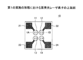
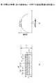
第1の実施の形態における面発光レーザ素子について説明する。本実施の形態における面発光レーザ素子10は、図1及び図2に示すように、複数の面発光レーザを有しており、具体的には、第1の面発光レーザ11、第2の面発光レーザ12、第3の面発光レーザ13、第4の面発光レーザ14を有している。尚、図1は本実施の形態の説明のため簡略化されており、便宜上コンタクト層等の記載は省略されている。また、図2は、図1における一点鎖線1A−1Bにおいて切断した断面図である。
[First Embodiment]
(Structure of surface emitting laser element)
The surface emitting laser element in the first embodiment will be described. As shown in FIGS. 1 and 2, the surface-emitting
本実施の形態における面発光レーザ素子10は、300μm角の半導体チップ上に形成されており、この半導体チップ上に形成された第1の面発光レーザ11、第2の面発光レーザ12、第3の面発光レーザ13、第4の面発光レーザ14は、各々に対応して設けられた電極パッドに接続されている。具体的には、第1の面発光レーザ11には電極パッド21が接続されており、第2の面発光レーザ12には電極パッド22が接続されており、第3の面発光レーザ13には電極パッド23が接続されており、第4の面発光レーザ14には電極パッド24が接続されている。
The surface emitting
また、第1の面発光レーザ11、第2の面発光レーザ12、第3の面発光レーザ13、第4の面発光レーザ14は、出射される光の波長が相互に異なるものである。即ち、第1の面発光レーザ11より出射される波長λ1、第2の面発光レーザ12より出射される波長λ2、第3の面発光レーザ13より出射される波長λ3、第4の面発光レーザ14より出射される波長λ4は、相互に異なる波長である。
The first
尚、本実施の形態における面発光レーザ素子は、発振波長が894.6nmとなる面発光レーザを得るためのものであり、300μm角の半導体チップ(基板)に4つの面発光レーザが形成されている。面発光レーザ素子では、狭い領域に複数の面発光レーザを形成することができるため、発光させる面発光レーザを切換えた場合であっても、発光位置は殆ど変わらない。従って、基板の大きさとしては、500μm×500μm以下の大きさとすることにより、光軸調整等が不要または極めて容易となる。 The surface-emitting laser element in this embodiment is for obtaining a surface-emitting laser having an oscillation wavelength of 894.6 nm. Four surface-emitting lasers are formed on a 300 μm-square semiconductor chip (substrate). Yes. In the surface emitting laser element, since a plurality of surface emitting lasers can be formed in a narrow area, even if the surface emitting laser to emit light is switched, the light emission position hardly changes. Therefore, by adjusting the size of the substrate to 500 μm × 500 μm or less, it is unnecessary or extremely easy to adjust the optical axis.
本実施の形態における面発光レーザ素子は、半導体等からなる基板101上に、屈折率の異なる半導体材料を交互に積層形成することにより、下部ブラッグ反射鏡102を形成し、下部ブラッグ反射鏡102上には、下部スペーサ層103、活性層104、上部スペーサ層105を形成する。上部スペーサ層105上には、第1の上部ブラッグ反射鏡106、コンタクト層110、波長調整領域120、第2の上部ブラッグ反射鏡107が形成されている。また、コンタクト層110の上には上部電極111が形成され接続されており、基板101の裏面には下部電極112が形成されている。本実施の形態では、コンタクト層110と波長調整領域120により波長調整層130が形成されているが、波長調整領域120に隣接してコンタクト層110が形成されていない場合には、波長調整層130は、波長調整領域120のみにより形成される場合がある。尚、基板101上に形成される半導体層となる下部ブラッグ反射鏡102、下部スペーサ層103、活性層104、上部スペーサ層105、第1の上部ブラッグ反射鏡106、コンタクト層110、波長調整領域120は、半導体材料をエピタキシャル成長させることにより形成されている。具体的には、これらの半導体層は、MOCVD(Metal Organic Chemical Vapor Deposition)またはMBE(Molecular Beam Epitaxy)によるエピタキシャル成長により形成されている。尚、本願明細書において記載されているブラッグ反射鏡は、DBRと記載される場合がある。
The surface emitting laser element according to the present embodiment forms a
また、波長調整層130の上には、第2の上部ブラッグ反射鏡107が各々の面発光レーザごとに形成されている。第2の上部ブラッグ反射鏡107は、酸化物、窒化物、フッ化物等からなる誘電体膜であって高屈折率材料膜と低屈折率材料膜とを交互に積層形成することにより形成されている。尚、本実施の形態では、第1の上部ブラッグ反射鏡106、波長調整層130、第2の上部ブラッグ反射鏡107により、上部ブラッグ反射鏡が形成されている。また、波長調整層130は、下部ブラッグ反射鏡102の内部に形成したものであってもよい。
On the
本実施の形態における面発光レーザ素子では、第1の面発光レーザ11、第2の面発光レーザ12、第3の面発光レーザ13、第4の面発光レーザ14において、各々波長調整層130における波長調整領域120の厚さが異なっている。具体的には、図3に示すように、波長調整領域120は、コンタクト層110の上に形成されており、波長調整領域120は、第1の調整層121、第2の調整層122、第3の調整層123により形成されている。本実施の形態では、第1の調整層121及び第3の調整層123はGaInPにより形成されており、第2の調整層122はGaAsPにより形成されている。尚、第1の調整層121、第2の調整層122、第3の調整層123を形成している材料は、この逆であってもよい。
In the surface emitting laser element according to the present embodiment, each of the first
このように本実施の形態における面発光レーザ素子は、第1の面発光レーザ11、第2の面発光レーザ12、第3の面発光レーザ13、第4の面発光レーザ14における波長調整領域120の厚さが異なるものである。
As described above, the surface emitting laser element according to the present embodiment includes the
具体的には、第1の面発光レーザ11には、波長調整領域120において、第1の調整層121、第2の調整層122、第3の調整層123が形成されており、この波長調整領域120とコンタクト層110との和である波長調整層130の厚さに対応した波長λ1の光が出射される。
Specifically, in the first
また、第2の面発光レーザ12には、波長調整領域120のうち、第1の調整層121、第2の調整層122が形成されており、この波長調整領域120とコンタクト層110との和である波長調整層130の厚さに対応した波長λ2の光が出射される。
Further, in the second
また、第3の面発光レーザ13には、波長調整領域120において、第1の調整層121が形成されており、この波長調整領域120とコンタクト層110との和である波長調整層130の厚さに対応した波長λ3の光が出射される。
The third
また、第4の面発光レーザ14には、波長調整領域120は形成されないため、コンタクト層110の厚さと等しい波長調整層130の厚さに対応した波長λ4の光が出射される。
Further, in the fourth
このようにして、第1の面発光レーザ11、第2の面発光レーザ12、第3の面発光レーザ13、第4の面発光レーザ14における波長調整層130の厚さを少しずつ変えることができ、波長調整層130における各々の厚さに対応した波長の光を各々出射させることができる。
In this manner, the thickness of the
(面発光レーザ素子の製造方法)
本実施の形態においては、基板101は、n−GaAs基板を用いている。また、下部ブラッグ反射鏡102は、n−Al0.1Ga0.9As高屈折率層とn−Al0.9Ga0.1As低屈折率層とを各々の層の光学的な膜厚がλ/4となるように35.5ペア積層することにより形成されている。
(Method for manufacturing surface-emitting laser element)
In the present embodiment, the
下部ブラッグ反射鏡102の上には、Al0.2Ga0.8Asからなる下部スペーサ層103を介し、GaInAs量子井戸層/GaInPAs障壁層からなる活性層104が形成されている。活性層104上には、Al0.2Ga0.8Asからなる上部スペーサ層105、第1の上部ブラッグ反射鏡106が形成されている。尚、下部スペーサ層103、活性層104、上部スペーサ層105により1波長光学厚さとなる共振器領域が形成されている。
An
第1の上部ブラッグ反射鏡106は、n−Al0.1Ga0.9As高屈折率層とn−Al0.9Ga0.1As低屈折率層とを各々の層の光学的な膜厚がλ/4となるように6ペア積層することにより形成されている。第1の上部ブラッグ反射鏡106の低屈折率層の一つは、AlAsからなる電流狭窄層108により形成されており、電流狭窄層108の周辺部分は選択酸化されて選択酸化領域108aが形成されており、中心部分は酸化されていない電流狭窄領域108bが形成されている。
The first
第1の上部ブラッグ反射鏡106の上には、p−GaAsからなるコンタクト層110、第1の調整層121、第2の調整層122、第3の調整層123からなる波長調整領域120が形成されている。尚、上述したように、各々の面発光レーザより出射される波長に対応して波長調整領域120における層の一部は除去されている。
On the first
本実施の形態における面発光レーザ素子では、各々の面発光レーザはメサ構造となっており、このメサ構造は、形成される面発光レーザ間の半導体層をエッチングにより除去することにより形成される。メサ構造を形成した後、水蒸気中で熱処理を行なうことにより、電流狭窄層108をメサ構造の周囲より酸化し、周辺部分の選択酸化領域108a(酸化されている領域)と中心部分の酸化されていない電流狭窄領域108bとが形成される。つまり、電流狭窄層108は、酸化された選択酸化領域108aと、酸化されていない電流狭窄領域108bとから構成されており、電流狭窄構造となっている。尚、メサ構造の上部より見た形状は、円形となるように形成してもよく、楕円形、正方形、長方形等の形状となるように形成してもよい。
In the surface emitting laser element in the present embodiment, each surface emitting laser has a mesa structure, and this mesa structure is formed by removing a semiconductor layer between formed surface emitting lasers by etching. After forming the mesa structure, the
また、各々の面発光レーザに対応してエッチングにより除去された波長調整層130の上には、第2の上部ブラッグ反射鏡107が形成されている。第2の上部ブラッグ反射鏡107はTiO2高屈折率層とSiO2低屈折率層とを各々の層の光学的な膜厚がλ/4となるように8.5ペア積層することにより形成されている。尚、第2の上部ブラッグ反射鏡107は、誘電体材料であって、高屈折率材料と低屈折率材料とを積層して形成したものであればよく、具体的には、酸化物、窒化物、フッ化物等の材料が挙げられる。高屈折率材料としては、TiO2の他、Ta2O5、HfO2等が挙げられる。また、低屈折率材料としては、SiO2の他、MgF2等が挙げられる。第2の上部ブラッグ反射鏡107におけるTiO2高屈折率層とSiO2低屈折率層の形成方法は、スパッタリングまたは真空蒸着等により形成される。更に、全体にはSiNからなる保護膜140が形成されており、各々の面発光レーザのメサの間にはポリイミド等の樹脂材料からなる樹脂層141が形成されている。
A second
この後、p側電極となる上部電極111を形成する。この上部電極111は、各々の面発光レーザに対応して各々形成されており、各々の上部電極111は、各々電極パッド21〜24と接続されている。また、基板101の裏面にはn側電極となる下部電極112が形成されている。
Thereafter, the
次に、本実施の形態における面発光レーザ素子における波長調整層130の形成方法について詳しく説明する。
Next, a method for forming the
最初に、基板101上に、半導体材料からなる下部ブラッグ反射鏡102、下部スペーサ層103、活性層104、上部スペーサ層105、第1の上部ブラッグ反射鏡106、コンタクト層110、波長調整領域120をMOCVDまたはMBEによるエピタキシャル成長より形成する。尚、波長調整層130は、コンタクト層110と波長調整領域120により形成されており、波長調整領域120は、第1の調整層121、第2の調整層122、第3の調整層123を積層することにより形成されている。ここで、前述したように、第1の調整層121及び第3の調整層123は、GaInPにより形成されており、第2の調整層122は、GaAsPにより形成されている。
First, a
次に、第1の面発光レーザ11が形成される領域にレジストパターンを形成する。具体的には、波長調整領域120における第3の調整層123上にフォトレジストを塗布し、露光装置による露光、現像を行なうことにより、レジストパターンを形成する。
Next, a resist pattern is formed in a region where the first
次に、レジストパターンの形成されていない領域の第3の調整層123をウエットエッチングにより除去する。具体的には、第3の調整層123は、GaInPにより形成されているため、塩酸と水の混合液によりウエットエッチングを行なう。これによりレジストパターンが形成されていない領域の第3の調整層123のみを除去し、第2の調整層122の表面を露出させる。尚、この混合液は、第3の調整層123を形成しているGaInPをエッチングすることはできるが、第2の調整層122を形成しているGaAsPは殆どエッチングすることができないものである。この混合液は第1のエッチング液とも記載する場合がある。この後、有機溶剤等によりレジストパターンを除去する。
Next, the
次に、第1の面発光レーザ11及び第2の面発光レーザ12が形成される領域にレジストパターンを形成する。具体的には、波長調整領域120の第3の調整層123及び第2の調整層122上にフォトレジストを塗布し、露光装置による露光、現像を行なうことにより、レジストパターンを形成する。
Next, a resist pattern is formed in a region where the first
次に、レジストパターンの形成されていない領域の第2の調整層122をウエットエッチングにより除去する。具体的には、第2の調整層122は、GaAsPにより形成されているため、硫酸と過酸化水素と水の混合液によりウエットエッチングを行なう。これによりレジストパターンが形成されていない領域の第2の調整層122のみを除去し、第1の調整層121の表面を露出させる。尚、この混合液は、第2の調整層122を形成しているGaAsPをエッチングすることはできるが、第1の調整層121を形成しているGaInPは殆どエッチングすることができないものである。この混合液を第2のエッチング液と記載する場合がある。この後、有機溶剤等によりレジストパターンを除去する。
Next, the
次に、第1の面発光レーザ11、第2の面発光レーザ12及び第3の面発光レーザ13が形成される領域にレジストパターンを形成する。具体的には、波長調整領域120における第1の調整層121、第2の調整層122及び第3の調整層123上にフォトレジストを塗布し、露光装置による露光、現像を行なうことにより、レジストパターンを形成する。
Next, a resist pattern is formed in a region where the first
次に、レジストパターンの形成されていない領域の第1の調整層121をウエットエッチングにより除去する。具体的には、第1のエッチング液によりレジストパターンの形成されていない領域の第1の調整層121を除去する。これによりレジストパターンが形成されていない領域の第1の調整層121のみを除去し、コンタクト層110の表面を露出させる。この後、有機溶剤等によりレジストパターンを除去する。
Next, the
次に、第2の上部ブラッグ反射鏡107を形成する。具体的には、スパッタリング等により、酸化物、窒化物、フッ化物等からなる高屈折率材料からなる誘電体膜と低屈折率材料からなる誘電体膜を所定の膜厚ごとに交互に積層することにより形成する。尚、第2の上部ブラッグ反射鏡107は、屈折率の異なる半導体材料を積層形成したものにより形成することも可能である。
Next, the second
これにより、本実施の形態における面発光レーザ素子における波長調整層130及び第2の上部ブラッグ反射鏡107を形成することができる。
Thereby, the
本実施の形態においては、波長調整層130における波長調整領域120を形成している第1の調整層121、第2の調整層122、第3の調整層123には、Alを含んでいないため、エッチング後に酸化等がされにくく、エッチング後もきれいな表面状態を維持することができる。即ち、Alは極めて腐食されやすいため、Alを含んだ材料により第1の調整層121、第2の調整層122、第3の調整層123のいずれかを形成した場合、ウエットエッチング等を行なった後の表面状態は劣悪なものとなり、この上に第2の上部ブラッグ反射鏡107を形成しても、剥がれてしまう場合や、厚さが不均一となる場合等がある。しかしながら、本実施の形態における面発光レーザ素子では、波長調整領域120はAlを含まない材料により形成されているため、Alの腐食等が生じることはなく、このような問題が生じることはない。
In the present embodiment, the
また、本実施の形態においては、波長調整層130における波長調整領域120は、GaAsPとGaInPとを交互に形成したものであり、ウエットエッチングを行う際には、相互に一方はエッチングをすることができるが他方はエッチングすることができない2種類のエッチング液を用いてエッチングを行なっている。このような2種類のエッチング液を用いてエッチングを行なうことにより、エッチング後の表面は平坦になり、オーバーエッチングされることなく所定の厚さで形成することができる。これにより、特性の安定した面発光レーザ素子を得ることができる。
In the present embodiment, the
尚、本実施の形態における説明では、GaAsPとGaInPとの組み合わせの場合について説明したが、Alを含まない材料であって、更にエッチング液が異なり、発振波長よりもバンドギャップエネルギーの大きい他の半導体材料の組み合わせでもよい。本実施の形態における発振波長である894.6nmの場合、このような半導体材料の組み合わせとしては、例えばGaInAsP/GaInP、GaAs/GaInP、GaAs/GaInAsP、GaAsP/GaInAsP等が挙げられる。また、GaAsN/GaInP、GaInNAs/GaInP、GaAsSb/GaInP等のようにN、Sbが添加されていてもよい。 In the description of the present embodiment, the case of a combination of GaAsP and GaInP has been described. However, other semiconductors that do not contain Al, have different etchants, and have a larger band gap energy than the oscillation wavelength. A combination of materials may be used. In the case of 894.6 nm which is the oscillation wavelength in this embodiment, examples of such a combination of semiconductor materials include GaInAsP / GaInP, GaAs / GaInP, GaAs / GaInAsP, and GaAsP / GaInAsP. Further, N and Sb may be added like GaAsN / GaInP, GaInNAs / GaInP, GaAsSb / GaInP, or the like.
以上により、本実施の形態における面発光レーザ素子では、1つの基板101において、波長の異なる光を出射する複数の面発光レーザを形成することができる。これにより、面発光レーザ素子を製造する際に半導体層等において膜厚変動が生じた場合であっても、所望の波長に最も近い波長の光を出射するものを第1の面発光レーザ11から第4の面発光レーザ14のうちから選ぶことにより、所望の波長の半導体レーザを容易に得ることができる。これにより、所定の波長で発光する面発光レーザを有する面発光レーザ素子を低コストで製造することができる。
As described above, in the surface emitting laser element according to the present embodiment, a plurality of surface emitting lasers that emit light having different wavelengths can be formed on one
尚、波長調整領域120の上にコンタクト層110を形成した場合では、波長調整領域120の厚さに依存して各々の面発光レーザに流すことのできる電流量等も変化し、各々の面発光レーザにおける電気的な特性及び発光特性も大きく異なるものとなる。また、波長調整領域120に電流を通す場合、各層の界面におけるバンド不連続により電気抵抗が増加してしまう。しかしながら、本実施の形態における面発光レーザ素子では、コンタクト層110は波長調整領域120の下に形成されているため、面発光レーザに注入される電流は波長調整領域120を通過することはなく、波長調整領域120の厚さに依存して抵抗等が変化することはない。
When the
次に、波長調整層130と共振器領域の間に形成される第1の上部ブラッグ反射鏡106の利点について説明する。例えば、波長調整層が1波長分の光学長を持つ共振器領域の中に形成されている場合、波長895nmを中心として波長1nm間隔で4波長とすると、波長調整層を構成する1層あたり1.3nmとなり、現状の結晶成長技術ではウエハ面内において均一に形成することは極めて困難である。そこで、本実施の形態においては、共振器領域と波長調整層130との間に上部ブラッグ反射鏡の一部となる第1の上部ブラッグ反射鏡106を形成する。具体的には、第1の上部ブラッグ反射鏡106として、n−Al0.1Ga0.9As高屈折率層とn−Al0.9Ga0.1As低屈折率層とを各々の層の光学的な膜厚がλ/4となるように6ペア積層することにより形成する。更に、第1の上部ブラッグ反射鏡106の上に、コンタクト層110を形成し、コンタクト層110の上に、波長調整領域120を形成する。波長調整領域120を形成している第1の調整層121、第2の調整層122及び第3の調整層123は、GaInP/GaAsP/GaInPの膜厚がそれぞれ16nm/16nm/16nmとなるように形成されており、現状の結晶成長技術で十分に均一に製造できるものである。よって、面発光レーザ間における波長間隔のバラつきを減らすことができる。
Next, advantages of the first
また、このような構造で形成することにより、同時に電気抵抗を低減させることもできる。即ち、波長調整層130の上部には誘電体による第2の上部ブラッグ反射鏡107が形成され、その周囲に上部電極111が形成されるが、共振器領域の中に波長調整層を設けた場合、層構造上、コンタクト層に近い位置にAlAs被選択酸化層を設ける必要があり電流経路が非常に狭くなり電気抵抗が増加する。そこで、本実施の形態では、波長調整層130(波長調整領域120の下にコンタクト層110が形成されている)と共振器領域との間に第1の上部ブラッグ反射鏡106を形成することにより、電流経路を拡大させることができ、電気抵抗を低減させることができる。
Moreover, by forming with such a structure, electrical resistance can be reduced simultaneously. That is, the second
尚、第2の上部ブラッグ反射鏡107を7ペア以上とすることにより、波長調整層130における波長調整領域120の各層の膜厚を更に増やすことができ、均一な製造が容易となり、電気抵抗も低減する。しかしながら、第2の上部ブラッグ反射鏡107におけるペア数が増えると、波長調整層130における光学厚さがλ/4より大きくなり、上部ブラッグ反射鏡全体の反射率が低下してしまう。このように第2の上部ブラッグ反射鏡107には、波長調整層130の光学的厚さをλ/4に近くすることができるような最適ペア数が存在する。
By setting the second
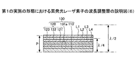
次に、波長調整層130の厚さについて説明する。図4(a)に示されるように、波長調整層130の光学的な厚さPが、λ/4≦P<λ/2である場合には、図4(b)に示されるように、第1の面発光レーザ11、第2の面発光レーザ12、第3の面発光レーザ13、第4の面発光レーザ14における上部ブラッグ反射鏡の反射率を略一定にすることができる。尚、L1は第1の面発光レーザ11における波長調整層130の表面であり、L2は第2の面発光レーザ12における波長調整層130の表面であり、L3は第3の面発光レーザ13における波長調整層130の表面であり、L4は第4の面発光レーザ14における波長調整層130の表面を示す。
Next, the thickness of the
一方、図5(a)に示されるように、波長調整層130の光学的な厚さPが、λ/2<Pである場合には、図5(b)に示されるように、第1の面発光レーザ11、第2の面発光レーザ12、第3の面発光レーザ13、第4の面発光レーザ14における上部ブラッグ反射鏡の反射率が大きく異なってしまう。
On the other hand, as shown in FIG. 5A, when the optical thickness P of the
また、図6(a)に示されるように、波長調整層130の光学的な厚さPが、P<λ/4である場合には、図6(b)に示されるように、第1の面発光レーザ11、第2の面発光レーザ12、第3の面発光レーザ13、第4の面発光レーザ14における上部ブラッグ反射鏡の反射率が大きく異なってしまう。
Further, as shown in FIG. 6A, when the optical thickness P of the
以上より、波長調整層130の光学的な厚さPは、
λ/4≦P<λ/2
であることが好ましく、このことを一般化するならば、
(2N−1)λ/4≦P<Nλ/2
であることが好ましい。尚、Nは正の整数であるが、光吸収の影響を受け、閾値電流の増加などの弊害を考慮した場合には、Nは小さい方が好ましい。
From the above, the optical thickness P of the
λ / 4 ≦ P <λ / 2
It is preferable that if this is generalized,
(2N-1) λ / 4 ≦ P <Nλ / 2
It is preferable that Note that N is a positive integer, but it is preferable that N is small in view of adverse effects such as an increase in threshold current due to the influence of light absorption.
また、波長調整領域120の厚さが薄く、波長調整領域120とコンタクト層110の光学的な厚さの和がλ/4未満の場合には、図7(a)に示すように波長調整層130に位相調整領域131を設けてもよい。これにより、波長調整層130における光学的な厚さPをλ/4≦P<λ/2、一般的には、(2N−1)λ/4≦P<2Nλ/4とすることができ、図7(b)に示されるように、第1の面発光レーザ11、第2の面発光レーザ12、第3の面発光レーザ13、第4の面発光レーザ14における上部ブラッグ反射鏡の反射率を略一定にすることができる。尚、この場合、波長調整層130は、コンタクト層110、波長調整領域120、位相調整領域131により形成される。また、位相調整領域131は、AlGaAsにより形成されており、図7(a)に示すように、位相調整領域131は、コンタクト層110の下に形成してもよく、図8に示すように、位相調整領域131は、コンタクト層110と波長調整領域120との間に形成してもよい。更には、図9に示すように、位相調整領域131aをGaAsPとGaInPとを交互に積層した積層膜により形成してもよい。
When the
また、本実施の形態における面発光レーザ素子は、波長調整領域120において複数の膜を形成した構造のものであるが、波長調整層130において、光学的な膜厚がλ/4となる位置は、形成されている膜(調整層)の層数をMとした場合(Mは正の整数)、Mが奇数の場合には、上から(M+1)/2番目の膜(調整層)であり、Mが偶数の場合には、上からM/2番目または、(M/2)+1番目の膜(調整層)となるように形成されていることが好ましい。
The surface-emitting laser element in the present embodiment has a structure in which a plurality of films are formed in the
〔第2の実施の形態〕
次に、第2の実施の形態における面発光レーザ素子について説明する。尚、本実施の形態における面発光レーザ素子は、波長が894.6nmの面発光レーザであって、波長調整領域が下部ブラッグ反射鏡に設けられている構造のものである。本実施の形態における面発光レーザ素子150は、図10及び図11に示すように、複数の面発光レーザを有しており、具体的には、第1の面発光レーザ151、第2の面発光レーザ152、第3の面発光レーザ153、第4の面発光レーザ154を有している。尚、図10は本実施の形態の説明のため簡略化されており、便宜上コンタクト層等の記載は省略されている。また、図11は、図10における一点鎖線10A−10Bにおいて切断した断面図である。
[Second Embodiment]
Next, a surface emitting laser element according to the second embodiment will be described. The surface emitting laser element in the present embodiment is a surface emitting laser having a wavelength of 894.6 nm and has a structure in which a wavelength adjustment region is provided in the lower Bragg reflector. As shown in FIGS. 10 and 11, the surface-emitting
本実施の形態における面発光レーザ素子150は、300μm角の半導体チップ上に形成されており、この半導体チップ上に形成された第1の面発光レーザ151、第2の面発光レーザ152、第3の面発光レーザ153、第4の面発光レーザ154は、各々に対応して設けられた電極パッドに接続されている。具体的には、第1の面発光レーザ151には電極パッド161が接続されており、第2の面発光レーザ152には電極パッド162が接続されており、第3の面発光レーザ153には電極パッド163が接続されており、第4の面発光レーザ154には電極パッド164が接続されている。
The surface emitting
また、第1の面発光レーザ151、第2の面発光レーザ152、第3の面発光レーザ153、第4の面発光レーザ154は、出射される光の波長が相互に異なるものである。即ち、第1の面発光レーザ151より出射される波長λ1、第2の面発光レーザ152より出射される波長λ2、第3の面発光レーザ153より出射される波長λ3、第4の面発光レーザ154より出射される波長λ4は、相互に異なる波長である。
The first surface-emitting
尚、本実施の形態における面発光レーザ素子は、発振波長が894.6nmとなる面発光レーザを得るためのものであり、300μm角の半導体チップ(基板)に4つの面発光レーザが形成されている。面発光レーザ素子では、狭い領域に複数の面発光レーザを形成することができるため、発光させる面発光レーザを切換えた場合であっても、発光位置は殆ど変わらない。 The surface-emitting laser element in this embodiment is for obtaining a surface-emitting laser having an oscillation wavelength of 894.6 nm. Four surface-emitting lasers are formed on a 300 μm-square semiconductor chip (substrate). Yes. In the surface emitting laser element, since a plurality of surface emitting lasers can be formed in a narrow area, even if the surface emitting laser to emit light is switched, the light emission position hardly changes.
本実施の形態における面発光レーザ素子は、半導体等からなる基板101上に、屈折率の異なる半導体材料を交互に積層形成することにより、第1の下部ブラッグ反射鏡172を形成し、第1の下部ブラッグ反射鏡172上には、位相調整領域173、波長調整領域180、第2の下部ブラッグ反射鏡174、下部スペーサ層103、活性層104、上部スペーサ層105が形成されている。上部スペーサ層105上には、上部ブラッグ反射鏡176、コンタクト層177が形成されている。また、コンタクト層177の上には上部電極178が形成され接続されており、基板101の裏面には下部電極112が形成されている。尚、本実施の形態では、波長調整領域180と位相調整領域173とにより波長調整層190が形成されており、第1の下部ブラッグ反射鏡172、位相調整領域173、波長調整領域180、第2の下部ブラッグ反射鏡174により、下部ブラッグ反射鏡170が形成されている。
In the surface emitting laser element according to the present embodiment, the first
また、基板101上に形成される半導体層となる第1の下部ブラッグ反射鏡172、位相調整領域173、波長調整領域180、第2の下部ブラッグ反射鏡174、下部スペーサ層103、活性層104、上部スペーサ層105、上部ブラッグ反射鏡176、コンタクト層177は、半導体材料をエピタキシャル成長させることにより形成されている。具体的には、これらの半導体層は、MOCVDまたはMBEによるエピタキシャル成長により形成されている。
In addition, a first
本実施の形態における面発光レーザ素子では、第1の面発光レーザ151、第2の面発光レーザ152、第3の面発光レーザ153、第4の面発光レーザ154において、各々の波長調整領域180の厚さが異なっている。具体的には、波長調整領域180は、第1の調整層181、第2の調整層182、第3の調整層183により形成されている。本実施の形態では、第1の調整層181及び第3の調整層183はGaInPにより形成されており、第2の調整層182はGaAsPにより形成されている。尚、第1の調整層181、第2の調整層182、第3の調整層183を形成している材料は、この逆であってもよい。
In the surface emitting laser element according to the present embodiment, in each of the first
このように本実施の形態における面発光レーザ素子は、第1の面発光レーザ151、第2の面発光レーザ152、第3の面発光レーザ153、第4の面発光レーザ154における波長調整領域180の厚さ、即ち、波長調整層190の厚さが異なるものである。
As described above, the surface emitting laser element according to this embodiment includes the wavelength adjustment region 180 in the first
具体的には、第1の面発光レーザ151には、波長調整領域180において、第1の調整層181、第2の調整層182、第3の調整層183が形成されており、この波長調整領域180を含む波長調整層190の厚さに対応した波長λ1の光が出射される。
Specifically, in the first
また、第2の面発光レーザ152には、波長調整領域180のうち、第1の調整層181、第2の調整層182が形成されており、この波長調整領域180を含む波長調整層190の厚さに対応した波長λ2の光が出射される。
The second
また、第3の面発光レーザ153には、波長調整領域180において、第1の調整層181が形成されており、この波長調整領域180を含む波長調整層190の厚さに対応した波長λ3の光が出射される。
The third
また、第4の面発光レーザ154には、波長調整領域180は形成されないため、波長調整領域180が形成されていない場合の波長調整層190の厚さに対応した波長λ4の光が出射される。
In addition, since the wavelength adjustment region 180 is not formed in the fourth
このようにして、第1の面発光レーザ151、第2の面発光レーザ152、第3の面発光レーザ153、第4の面発光レーザ154における波長調整領域180の厚さを少しずつ変えることができ、波長調整領域180における各々の厚さに対応した波長の光を各々出射させることができる。
In this way, the thickness of the wavelength adjustment region 180 in the first
本実施の形態においては、基板101は、n−GaAs基板を用いている。また、下部ブラッグ反射鏡170は、n−Al0.1Ga0.9As高屈折率層とn−Al0.9Ga0.1As低屈折率層とを各々の層の光学的な膜厚がλ/4となるように35.5ペア積層することにより形成されている。
In the present embodiment, the
下部ブラッグ反射鏡170は前述したように、基板101の上に、第1の下部ブラッグ反射鏡172、位相調整領域173、波長調整領域180、第2の下部ブラッグ反射鏡174により形成されている。従って、位相調整領域173及び波長調整領域180は、下部ブラッグ反射鏡170の内部に形成されている。尚、本実施の形態においては、図12に示されるように、位相調整領域173の光学的な膜厚と波長調整領域180の光学的な膜厚の半分との和、即ち、位相調整領域173の下部から波長調整領域180の中心部分までの光学的な膜厚がλ/4となるように形成されている。
As described above, the lower Bragg reflector 170 is formed on the
下部ブラッグ反射鏡170の上には、Al0.2Ga0.8Asからなる下部スペーサ層103を介し、GaInAs量子井戸層/GaInPAs障壁層からなる活性層104が形成されている。活性層104上には、Al0.2Ga0.8Asからなる上部スペーサ層105が形成されている。尚、下部スペーサ層103、活性層104、上部スペーサ層105により1波長光学厚さとなる共振器領域が形成されている。
An
上部ブラッグ反射鏡176は、n−Al0.1Ga0.9As高屈折率層とn−Al0.9Ga0.1As低屈折率層とを各々の層の光学的な膜厚がλ/4となるように24ペア積層することにより形成されている。上部ブラッグ反射鏡176の低屈折率層の一つは、AlAsからなる電流狭窄層108により形成されており、電流狭窄層108の周辺部分は選択酸化されて選択酸化領域108aが形成されており、中心部分は酸化されていない電流狭窄領域108bが形成されている。また、上部ブラッグ反射鏡176の上には、p−GaAsからなるコンタクト層177が形成されている。
Top Bragg reflector 176, the optical thickness of the n-Al 0.1 Ga 0.9 As high refractive index layer and the n-Al 0.9 Ga 0.1 As low refractive index layer and each layer It is formed by laminating 24 pairs so that λ / 4. One of the low refractive index layers of the
図12(a)に示されるように、位相調整領域173の光学的な膜厚の値と波長調整領域180の光学的な膜厚の半分の値との和が約λ/4である場合には、図12(b)に示されるように、第1の面発光レーザ151、第2の面発光レーザ152、第3の面発光レーザ153、第4の面発光レーザ154における下部ブラッグ反射鏡の反射率を略一定にすることができる。尚、L1は第1の面発光レーザ151における波長調整層190の表面であり、L2は第2の面発光レーザ152における波長調整層190の表面であり、L3は第3の面発光レーザ153における波長調整層190の表面であり、L4は第4の面発光レーザ154における波長調整層190の表面を示す。
As shown in FIG. 12A, when the sum of the optical film thickness value of the
本実施の形態における面発光レーザ素子では、各々の面発光レーザはメサ構造となっており、このメサ構造は、形成される面発光レーザ間の半導体層をドライエッチング等により除去することにより形成される。メサ構造を形成した後、水蒸気中で熱処理を行なうことにより、電流狭窄層108をメサ構造の周囲より酸化し、周辺部分の選択酸化領域108a(酸化されている領域)と中心部分の酸化されていない電流狭窄領域108bとが形成される。つまり、電流狭窄層108は、酸化された選択酸化領域108aと、酸化されていない電流狭窄領域108bとから構成されており、電流狭窄構造となっている。具体的には、電流狭窄層108を形成しているAlAsを水蒸気中で熱処理することにより酸化させてAlxOyを形成し、このように形成されたAlxOyにより選択酸化領域108aが形成される。この際、電流狭窄層108において酸化されていないAlAsにより電流狭窄領域108bが形成される。尚、メサ構造の上部より見た形状は、円形となるように形成してもよく、楕円形、正方形、長方形等の形状となるように形成してもよい。
In the surface emitting laser element according to the present embodiment, each surface emitting laser has a mesa structure, and this mesa structure is formed by removing a semiconductor layer between formed surface emitting lasers by dry etching or the like. The After forming the mesa structure, the
更に、全体にはSiNからなる保護膜140が形成されており、各々の面発光レーザのメサの間にはポリイミド等の樹脂材料を埋め込むことにより樹脂層141が形成されている。この後、p側電極となる上部電極178を形成する。この上部電極178は、各々の面発光レーザに対応して各々形成されており、各々の上部電極178は、各々電極パッド161〜164と接続されている。
Further, a
具体的には、SiNからなる保護膜140を形成し、各々の面発光レーザのメサの間にポリイミド等の樹脂材料を埋め込み平坦化することにより樹脂層141を形成する。この後、コンタクト層177の上の保護膜140及び樹脂層141を除去し、コンタクト層177を露出させ、コンタクト層177の上に、上部電極178を形成する。尚、基板101の裏面にはn側電極となる下部電極112が形成されている。
Specifically, a
本実施の形態における面発光レーザ素子は、基板101側とは反対側にレーザ光が出射されるものである。尚、本実施の形態においては、SiNにより形成されている保護膜140により、メサエッチングで現れた腐食しやすいAlを含む層の側面や底面を誘電体により保護することができるため、信頼性を向上させることができる。
The surface emitting laser element according to the present embodiment emits laser light on the side opposite to the
次に、波長調整領域180と共振器の間に形成される第2の下部ブラッグ反射鏡174の利点について説明する。波長調整領域が1波長分の光学長を持つ共振器の中に形成されている場合、波長895nmを中心として波長1nm間隔で4波長とすると、波長調整領域を構成する調整層の1層あたりが1nm程度となり、現状の結晶成長技術ではウエハ面内における均一化は極めて困難である。
Next, advantages of the second
そこで、本実施の形態においては、共振器と波長調整領域180の間に下部ブラッグ反射鏡170の一部となる第2の下部ブラッグ反射鏡174を形成する。具体的には、第2の下部ブラッグ反射鏡174として、n−Al0.1Ga0.9As高屈折率層とn−Al0.9Ga0.1As低屈折率層とを各々の層の光学的な膜厚がλ/4となるように10ペア積層することにより形成する。これにより、波長調整領域180を形成している第1の調整層181、第2の調整層182及び第3の調整層183におけるGaInP/GaAsP/GaInPの膜厚が、それぞれ16nm/16nm/16nmとすることができ、現状の結晶成長技術により十分に均一に製造することができるため、第1の実施の形態と同様に、波長間隔のバラつきを改善することができる。
Therefore, in the present embodiment, a second
尚、第2の下部ブラッグ反射鏡174を11ペア以上形成した場合、波長調整領域180における各々の層の膜厚をより一層厚くすることが可能であるため、均一性をさらに高めることができる。しかしながら、図13に示されるように、第2の下部ブラッグ反射鏡174におけるペア数が増加すると、波長調整領域180における光学膜厚がλ/4(ブラッグ反射鏡の光学膜厚)より大幅に厚くなるため、下部ブラッグ反射鏡170全体の反射率が低下してしまい好ましくない。このように第2の下部ブラッグ反射鏡には、波長調整領域180の光学的膜厚がλ/4に近くなるべき最適ペア数が存在する。
When 11 pairs or more of the second
一方、図13(a)に示されるように、位相調整領域173の光学的な膜厚の値と波長調整領域180の光学的な膜厚の半分の値との和がλ/4以上である場合には、図13(b)に示されるように、第1の面発光レーザ151、第2の面発光レーザ152、第3の面発光レーザ153、第4の面発光レーザ154における各々の下部ブラッグ反射鏡の反射率が大きく異なってしまう。これに対し、本実施の形態においては、図12(b)に示されるように、各々の下部ブラッグ反射鏡における反射率の均一性を高めることができる。
On the other hand, as shown in FIG. 13A, the sum of the optical film thickness value of the
次に、本実施の形態における面発光レーザ素子における波長調整領域180の形成方法について詳しく説明する。 Next, a method for forming the wavelength adjustment region 180 in the surface emitting laser element according to the present embodiment will be described in detail.
最初に、基板101上に、半導体材料からなる第1の下部ブラッグ反射鏡172、位相調整領域173、波長調整領域180をMOCVDまたはMBEによるエピタキシャル成長より形成する。前述したように、波長調整層190は、位相調整領域173と波長調整領域180により形成されており、波長調整領域180は、第1の調整層181、第2の調整層182、第3の調整層183を積層することにより形成されている。尚、第1の調整層181及び第3の調整層183は、GaInPにより形成されており、第2の調整層182は、GaAsPにより形成されている。
First, a first
次に、第1の面発光レーザ151が形成される領域にレジストパターンを形成する。具体的には、波長調整領域180における第3の調整層183上にフォトレジストを塗布し、露光装置による露光、現像を行なうことにより、レジストパターンを形成する。
Next, a resist pattern is formed in a region where the first
次に、レジストパターンの形成されていない領域の第3の調整層183をウエットエッチングにより除去する。具体的には、第3の調整層183は、GaInPにより形成されているため、塩酸と水の混合液によりウエットエッチングを行なう。これによりレジストパターンが形成されていない領域の第3の調整層183のみを除去し、第2の調整層182の表面を露出させる。尚、この混合液は、第3の調整層183を形成しているGaInPをエッチングすることはできるが、第2の調整層182を形成しているGaAsPは殆どエッチングすることができない。この混合液は第1のエッチング液とも記載する場合がある。この後、有機溶剤等によりレジストパターンを除去する。
Next, the
次に、第1の面発光レーザ151及び第2の面発光レーザ152が形成される領域にレジストパターンを形成する。具体的には、波長調整領域180の第3の調整層183及び第2の調整層182上にフォトレジストを塗布し、露光装置による露光、現像を行なうことにより、レジストパターンを形成する。
Next, a resist pattern is formed in a region where the first
次に、レジストパターンの形成されていない領域の第2の調整層182をウエットエッチングにより除去する。具体的には、第2の調整層182は、GaAsPにより形成されているため、硫酸と過酸化水素と水の混合液によりウエットエッチングを行なう。これによりレジストパターンが形成されていない領域の第2の調整層182のみを除去し、第1の調整層181の表面を露出させる。尚、この混合液は、第2の調整層182を形成しているGaAsPをエッチングすることはできるが、第1の調整層181を形成しているGaInPは殆どエッチングすることができない。この混合液を第2のエッチング液と記載する場合がある。この後、有機溶剤等によりレジストパターンを除去する。
Next, the second adjustment layer 182 in the region where the resist pattern is not formed is removed by wet etching. Specifically, since the second adjustment layer 182 is formed of GaAsP, wet etching is performed using a mixed solution of sulfuric acid, hydrogen peroxide, and water. Thereby, only the second adjustment layer 182 in the region where the resist pattern is not formed is removed, and the surface of the
次に、第1の面発光レーザ151、第2の面発光レーザ152及び第3の面発光レーザ153が形成される領域にレジストパターンを形成する。具体的には、波長調整領域180における第1の調整層181、第2の調整層182及び第3の調整層183上にフォトレジストを塗布し、露光装置による露光、現像を行なうことにより、レジストパターンを形成する。
Next, a resist pattern is formed in a region where the first
次に、レジストパターンの形成されていない領域の第1の調整層181をウエットエッチングにより除去する。具体的には、第1のエッチング液によりレジストパターンの形成されていない領域の第1の調整層181を除去する。これによりレジストパターンが形成されていない領域の第1の調整層181のみを除去し、位相調整領域173の表面を露出させる。この後、有機溶剤等によりレジストパターンを除去する。
Next, the
次に、第2の下部ブラッグ反射鏡174を形成する。これにより、本実施の形態における面発光レーザ素子における波長調整領域180を含む下部ブラッグ反射鏡170を形成することができる。
Next, a second
本実施の形態では、波長調整層190において波長調整領域180を形成している第1の調整層181、第2の調整層182、第3の調整層183には、Alが含まれていないため、エッチング後に酸化等がされにくく、エッチング後もきれいな表面状態を維持することができる。即ち、Alは極めて腐食されやすいため、Alを含んだ材料により第1の調整層181、第2の調整層182、第3の調整層183のいずれかを形成した場合、ウエットエッチング等を行なった後の表面状態は劣悪なものとなり、この上に第2の下部ブラッグ反射鏡174を形成しても、剥がれてしまう場合や、厚さが不均一となる場合等がある。しかしながら、本実施の形態における面発光レーザ素子では、波長調整領域180はAlを含まない材料により形成されているため、Alの腐食等が生じることはなく、このような問題が生じることはない。
In the present embodiment, the
また、本実施の形態では、波長調整層190における波長調整領域180は、GaAsPとGaInPとを交互に形成したものであり、ウエットエッチングを行う際には、相互に一方はエッチングをすることができるが他方はエッチングすることができない2種類のエッチング液を用いてエッチングを行なっている。このような2種類のエッチング液を用いてエッチングを行なうことにより、エッチング後の表面は平坦になり、オーバーエッチングされることなく所定の厚さで形成することができる。これにより、特性の安定した面発光レーザ素子を得ることができる。
In the present embodiment, the wavelength adjustment region 180 in the
尚、本実施の形態における説明では、GaAsPとGaInPとの組み合わせの場合について説明したが、Alを含まない材料であって、更にエッチング液が異なり、発振波長よりもバンドギャップエネルギーの大きい他の半導体材料の組み合わせでもよい。本実施の形態における発振波長である894.6nmの場合、このような半導体材料の組み合わせとしては、例えばGaInAsP/GaInP、GaAs/GaInP、GaAs/GaInAsP、GaAsP/GaInAsP等が挙げられる。また、GaAsN/GaInP、GaInNAs/GaInP、GaAsSb/GaInP等のようにN、Sbが添加されていてもよい。 In the description of the present embodiment, the case of a combination of GaAsP and GaInP has been described. However, other semiconductors that do not contain Al, have different etchants, and have a larger band gap energy than the oscillation wavelength. A combination of materials may be used. In the case of 894.6 nm which is the oscillation wavelength in this embodiment, examples of such a combination of semiconductor materials include GaInAsP / GaInP, GaAs / GaInP, GaAs / GaInAsP, and GaAsP / GaInAsP. Further, N and Sb may be added like GaAsN / GaInP, GaInNAs / GaInP, GaAsSb / GaInP, or the like.
以上により、本実施の形態における面発光レーザ素子では、1つの基板101において、波長の異なる光を出射する複数の面発光レーザを形成することができる。これにより、面発光レーザ素子を製造する際に半導体層等において膜厚変動が生じた場合であっても、所望の波長に最も近い波長の光を出射するものを第1の面発光レーザ151から第4の面発光レーザ154のうちから選ぶことにより、所望の波長の半導体レーザを容易に得ることができる。これにより、所定の波長で発光する面発光レーザを有する面発光レーザ素子を低コストで製造することができる。
As described above, in the surface emitting laser element according to the present embodiment, a plurality of surface emitting lasers that emit light having different wavelengths can be formed on one
尚、上記以外の内容については、第1の実施の形態と同様である。 The contents other than the above are the same as in the first embodiment.
〔第3の実施の形態〕
次に、第3の実施の形態について説明する。本実施の形態における面発光レーザは、波長780nmの12chの面発光レーザ素子であり、図14及び図15に基づき説明する。尚、図14は、本実施の形態における面発光レーザ素子の上面図であり、図15(a)は、図14における一点鎖線14A−14Bにおいて切断した断面図、図15(b)は、図14における一点鎖線14C−14Dにおいて切断した断面図である。
[Third Embodiment]
Next, a third embodiment will be described. The surface emitting laser in the present embodiment is a 12ch surface emitting laser element having a wavelength of 780 nm, and will be described with reference to FIGS. 14 is a top view of the surface emitting laser element according to the present embodiment. FIG. 15A is a cross-sectional view taken along the alternate long and short dash line 14A-14B in FIG. 14, and FIG. 14 is a cross-sectional view taken along an alternate long and short dash line 14C-14D in FIG.
本実施の形態における面発光レーザ素子200は、300μm角の半導体チップ上に形成されており、この半導体チップ上に形成された第1の面発光レーザ201、第2の面発光レーザ202、第3の面発光レーザ203、第4の面発光レーザ204、第5の面発光レーザ205、第6の面発光レーザ206、第7の面発光レーザ207、第8の面発光レーザ208、第9の面発光レーザ209、第10の面発光レーザ210、第11の面発光レーザ211、第12の面発光レーザ212は、各々に対応して設けられた電極パッドに接続されている。
The surface emitting
具体的には、第1の面発光レーザ201には電極パッド221が接続されており、第2の面発光レーザ202には電極パッド222が接続されており、第3の面発光レーザ203には電極パッド223が接続されており、第4の面発光レーザ204には電極パッド224が接続されており、第5の面発光レーザ205には電極パッド225が接続されており、第6の面発光レーザ206には電極パッド226が接続されており、第7の面発光レーザ207には電極パッド227が接続されており、第8の面発光レーザ208には電極パッド228が接続されており、第9の面発光レーザ209には電極パッド229が接続されており、第10の面発光レーザ210には電極パッド230が接続されており、第11の面発光レーザ211には電極パッド231が接続されており、第12の面発光レーザ212には電極パッド232が接続されている。
Specifically, an
また、第1の面発光レーザ201、第2の面発光レーザ202、第3の面発光レーザ203、第4の面発光レーザ204、第5の面発光レーザ205、第6の面発光レーザ206、第7の面発光レーザ207、第8の面発光レーザ208、第9の面発光レーザ209、第10の面発光レーザ210、第11の面発光レーザ211、第12の面発光レーザ212は、出射される光の波長が相互に異なるものである。即ち、第1の面発光レーザ201より出射される波長λ1、第2の面発光レーザ202より出射される波長λ2、第3の面発光レーザ203より出射される波長λ3、第4の面発光レーザ204より出射される波長λ4、第5の面発光レーザ205より出射される波長λ5、第6の面発光レーザ206より出射される波長λ6、第7の面発光レーザ207より出射される波長λ7、第8の面発光レーザ208より出射される波長λ8、第9の面発光レーザ209より出射される波長λ9、第10の面発光レーザ210より出射される波長λ10、第11の面発光レーザ211より出射される波長λ11、第12の面発光レーザ212より出射される波長λ12は、相互に異なる波長である。
The first
本実施の形態における面発光レーザ素子は、半導体等からなる基板101上に、下部ブラッグ反射鏡102、下部スペーサ層103、活性層104、上部スペーサ層105、第1の上部ブラッグ反射鏡106が形成されており、第1の上部ブラッグ反射鏡106の上には、第1の波長調整層250、第2の上部ブラッグ反射鏡271、第2の波長調整層260、第3の上部ブラッグ反射鏡272、コンタクト層240、上部電極111が形成されている。また、コンタクト層240は上部電極111と接続されており、基板101の裏面には下部電極112が形成されている。尚、本実施の形態では、基板101上に形成される半導体層となる下部ブラッグ反射鏡102、下部スペーサ層103、活性層104、上部スペーサ層105、第1の上部ブラッグ反射鏡106、第1の波長調整層250、第2の上部ブラッグ反射鏡271、第2の波長調整層260、第3の上部ブラッグ反射鏡272、コンタクト層240は、半導体材料をエピタキシャル成長させることにより形成されている。具体的には、これら半導体層は、MOCVDまたはMBEによるエピタキシャル成長により形成されている。尚、本実施の形態では、第1の上部ブラッグ反射鏡106、第1の波長調整層250、第2の上部ブラッグ反射鏡271、第2の波長調整層260、第3の上部ブラッグ反射鏡272により上部ブラッグ反射鏡が形成されている。また、第1の波長調整層250、第2の波長調整層260は下部ブラッグ反射鏡102の内部に形成したものであってもよい。
In the surface emitting laser element according to the present embodiment, a
本実施の形態においては、基板101は、n−GaAs基板を用いている。また、下部ブラッグ反射鏡102は、n−Al0.1Ga0.9As高屈折率層とn−Al0.9Ga0.1As低屈折率層とを各々の層の光学的な膜厚がλ/4となるように35.5ペア積層することにより形成されている。
In the present embodiment, the
下部ブラッグ反射鏡102の上には、Al0.2Ga0.8Asからなる下部スペーサ層103を介し、GaInAs量子井戸層/GaInPAs障壁層からなる活性層104が形成されている。活性層104上には、Al0.2Ga0.8Asからなる上部スペーサ層105、第1の上部ブラッグ反射鏡106が形成されている。尚、下部スペーサ層103、活性層104、上部スペーサ層105は1波長光学厚さとなる共振器領域が形成されている。
An
第1の上部ブラッグ反射鏡106は、n−Al0.1Ga0.9As高屈折率層とn−Al0.9Ga0.1As低屈折率層とを各々の層の光学的な膜厚がλ/4となるように3.5ペア積層することにより形成されている。尚、第1の上部ブラッグ反射鏡106の低屈折率層の一つは、図15には不図示のAlAsからなる電流狭窄層により形成されている。
The first
第1の上部ブラッグ反射鏡106の上には、第1の波長調整層250が形成されている。第1の波長調整層250は、p−Al0.1Ga0.9Asからなる位相調整領域254、GaInPからなる第1の調整層251、GaAsPからなる第2の調整層252、GaInPからなる第3の調整層253を積層することにより形成されている。
A first
第1の波長調整層250の上には、第2の上部ブラッグ反射鏡271が形成されている。第2の上部ブラッグ反射鏡271は、n−Al0.1Ga0.9As高屈折率層とn−Al0.9Ga0.1As低屈折率層とを各々の層の光学的な膜厚がλ/4となるように4.5ペア積層することにより形成されている。
A second upper Bragg reflector 271 is formed on the first
第2の上部ブラッグ反射鏡271の上には、第2の波長調整層260が形成されている。第2の波長調整層260は、p−Al0.1Ga0.9Asからなる位相調整領域263、GaInPからなる第4の調整層261、GaAsPからなる第5の調整層262を積層することにより形成されている。 A second wavelength adjusting layer 260 is formed on the second upper Bragg reflector 271. The second wavelength adjustment layer 260 includes a phase adjustment region 263 made of p-Al 0.1 Ga 0.9 As, a fourth adjustment layer 261 made of GaInP, and a fifth adjustment layer 262 made of GaAsP. It is formed by.
第2の波長調整層260の上には、第3の上部ブラッグ反射鏡272が形成されている。第3の上部ブラッグ反射鏡272は、n−Al0.1Ga0.9As高屈折率層とn−Al0.9Ga0.1As低屈折率層とを各々の層の光学的な膜厚がλ/4となるように17ペア積層することにより形成されている。 A third upper Bragg reflector 272 is formed on the second wavelength adjustment layer 260. The third upper Bragg reflector 272 includes an n-Al 0.1 Ga 0.9 As high-refractive index layer and an n-Al 0.9 Ga 0.1 As low-refractive index layer. It is formed by laminating 17 pairs so that the film thickness becomes λ / 4.
第3の上部ブラッグ反射鏡272の上には、p−GaAsからなるコンタクト層240が形成されており、コンタクト層240の上には上部電極111が形成され、基板101の裏面には下部電極112が形成されている。
A
本実施の形態では、各々の面発光レーザに対応して各々のchごとに、第1の波長調整層250及び第2の波長調整層260が異なる厚さとなるように形成されている。尚、厚さの異なる第1の波長調整層250及び第2の波長調整層260は、第1の実施の形態と同様の方法により形成することができる。具体的には、フォトリソグラフィと選択的エッチングを行なうことにより、波長調整層の層数を異なるように形成することができる。例えば、GaAsP(GaAsの場合も同様)をエッチングする際には、硫酸、過酸化水素、水の混合液を用いることができ、GaInPをエッチングする際には、塩酸、水の混合液を用いることができる。第1の波長調整層250の選択エッチングを行なった後に、第2の上部ブラッグ反射鏡271及び第2の波長調整層260を結晶成長により形成し、第2の波長調整層260の選択エッチングを行い、第3の上部BDR272及びコンタクト層240を結晶成長により形成する。尚、各々の面発光レーザの形成に必要となるメサのエッチングは、ドライエッチング法により行なわれている。また、図15に示されるように、コンタクト層240上に各々面発光レーザのp側電極となる上部電極111を形成し、基板101の裏面にn側共通電極となる下部電極112を形成する。本実施の形態における面発光レーザ素子では、基板101と反対側にレーザ光が放射される。
In the present embodiment, the first
特許文献2では、波長調整層は1波長分の光学長を持つ共振器領域の中に形成されている。例えば、この場合、波長780nmを中心として波長3nm間隔とすると、波長調整層を構成する1層あたり0.9nmとなる。これは約3原子層に相当する厚さであり、現状の結晶成長技術ではウエハ面内において均一に形成することは困難である。また、X波長分(X=2、3、、、、、)の光学長を持つ共振器領域とすると、波長調整層を構成する1層あたり0.9×Xnmとなり膜厚が増加するが、この場合、緩和振動周波数がX−1/2倍だけ悪化し、高速変調動作が困難となるなどの弊害が生じる。
In
そこで、図15に示されるように、本実施の形態における面発光レーザ素子においては、共振器領域と第1の波長調整層250との間に第1の上部ブラッグ反射鏡106を形成する。具体的には、第1の波長調整層250と共振器領域との間に、4.5ペアのp-Al0.1Ga0.9As高屈折率層とn−Al0.9Ga0.1As低屈折率層とを交互に積層することにより第1の上部ブラッグ反射鏡106を形成する。この場合、異なる発光素子間での発振波長間隔を3nmとしても、第1の波長調整層250を形成しているGaInP/GaAsP/GaInPの膜厚は、それぞれ11.6nm/11.6nm/11.6nmとなり、現状の結晶成長技術で十分に均一に製造することができる。よって、面発光レーザ間における波長間隔のバラつきを減らすことができる。
Therefore, as shown in FIG. 15, in the surface emitting laser element according to the present embodiment, the first
また、更に、第1の波長調整層250の上に、第2の上部ブラッグ反射鏡271及び第2の波長調整層260を形成する。これにより、第1の波長調整層250をより均一に発振波長間隔を狭くして形成することができる。図16は、図14及び図15に示される本実施の形態における面発光レーザ素子において、第1の波長調整層250及び第2の波長調整層260の膜厚(光学的な膜厚で示す。λ/4を0.25とする。)と発振波長の関係を示す。尚、第1の波長調整層250の膜厚は、第1の波長調整層250を形成しているGaInP/GaAsP/GaInPについて選択エッチングをすることにより変化させることができる。同様に、第2の波長調整層260の膜厚は、第2の波長調整層260を形成しているGaInP/GaAsPについて選択エッチングをすることにより変化させることができる。
Furthermore, a second upper Bragg reflector 271 and a second wavelength adjustment layer 260 are formed on the first
図16に示されるように、第2の波長調整層260が同じ膜厚においては、第1の波長調整層250の膜厚を変化させること、即ち、第1の波長調整層250を形成している11.6nm/11.6nm/11.6nmのGaInP/GaAsP/GaInPを1層ずつエッチングすることで、約3nmの発振波長変化を得ることができる。また、第1の波長調整層250が同じ膜厚とし、第2の波長調整層260の膜厚を変化させること、即ち、第2の波長調整層260を形成している14nm/11nmのGaInP/GaAsPを1層ずつエッチングすることにより、約1nmの発振波長変化を得ることができる。このように、図15に示されるように、第1の波長調整層250及び第2の波長調整層260の膜厚をそれぞれ4水準及び3水準で変化させることで、4×3=12水準で発振波長を異なる面発光レーザを形成することができる。また、第1の波長調整層250及び第2の波長調整層260の膜厚を調整することにより、図16に示されるように、12個の面発光レーザを全て約1nm間隔の異なる波長で発振させることができる。
As shown in FIG. 16, when the second wavelength adjustment layer 260 has the same film thickness, the thickness of the first
次に、第1の波長調整層250に形成される位相調整領域254について説明する。図17(a)に示されるように、位相調整領域254を形成することなく第1の調整層251、第2の調整層252及び第3の調整層253を形成した場合において、GaInP/GaAsP/GaInPの各々の層をウエットエッチングにより除去した場合の反射率を図17(b)に示す。図17(b)に示されるように、位相調整領域254を形成しない場合には、第1の波長調整層250の厚さが変化することにより反射率が大きく変化してしまう。これは、各々の波長において閾値電流等のレーザ特性におけるバラツキが大きくなることを意味する。
Next, the
一方、図18(a)に示すように、第1の波長調整層250に位相調整領域254を形成することにより、第1の波長調整層250における光学的な厚さがλ/4となる位置をGaAsPからなる第2の調整層252が形成されている位置にすることができる。これにより、図18(b)に示されるように、反射率の変化を少なくすることができる。
On the other hand, as shown in FIG. 18A, by forming the
即ち、第1の波長調整層250の光学的な厚さP1は、
λ/4≦P1<λ/2
であることが好ましく、このことを一般化するならば、
(2N−1)λ/4≦P1<2Nλ/4
であることが好ましい。尚、Nは正の整数である。
That is, the optical thickness P1 of the first
λ / 4 ≦ P1 <λ / 2
It is preferable that if this is generalized,
(2N-1) λ / 4 ≦ P1 <2Nλ / 4
It is preferable that N is a positive integer.
また、第1の波長調整層250において光学的な膜厚がλ/4となる位置は、形成されている膜(調整層)の層数をMとした場合(Mは正の整数)、Mが奇数の場合には、上から(M+1)/2番目の膜(調整層)であり、Mが偶数の場合には、上からM/2番目または、(M/2)+1の膜(調整層)となるように形成されていることが好ましい。
Further, the position where the optical film thickness is λ / 4 in the first
図19(a)に示されるように、位相調整領域254は、p−Al0.1Ga0.9Asにより形成してもよく、図19(b)に示されるように、GaInP及びGaAsPを交互に積層することに位相調整領域254aを形成してもよい。尚、上記においては、第1の波長調整層250について説明したが、第2の波長調整層260についても同様である。
As shown in FIG. 19A, the
ところで、波長調整層としては、特許文献4ではAlGaAsとInGaPの組み合わせが開示されており、特許文献2ではGaAsとAlGaAsの組み合わせが開示されている。いずれもAlを含むAlGaAsを用いているが、Alを含んでいるので酸化など腐食しやすく信頼性に問題があった。特に、本実施の形態のように波長調整層のエッチング後に半導体層の結晶成長を行う場合においては、波長調整層表面は製造工程において大気に触れるため、Alの表面が酸化され、その上に上部ブラッグ反射鏡を結晶成長させることは極めて困難である。そこで、本実施の形態における面発光レーザ素子では、特許文献2、4とは異なり、Alを含まないGaInPとGaAsPとにより波長調整層を形成することにより、製造工程における腐食の進行を極めて遅くすることができ、高い信頼性を得ることができる。
By the way, as the wavelength adjustment layer,
尚、本実施の形態における説明では、GaAsPとGaInPとの組み合わせの場合について説明したが、Alを含まない材料であって、更にエッチング液が異なり、発振波長よりもバンドギャップエネルギーの大きい他の半導体材料の組み合わせでもよい。本実施の形態における発振波長である780nmの場合、このような半導体材料の組み合わせとしては、例えばGaInAsP/GaInP、GaAsP/GaInAsP等が挙げられる。また、波長が1μm以上の長波長においてはGaAsPの代わりにGaAsを用いこともできる。この場合には、GaAs基板に対してGaAsPのように歪を有していないので扱いやすい。 In the description of the present embodiment, the case of a combination of GaAsP and GaInP has been described. However, other semiconductors that do not contain Al, have different etchants, and have a larger band gap energy than the oscillation wavelength. A combination of materials may be used. In the case of the oscillation wavelength of 780 nm in the present embodiment, examples of such a combination of semiconductor materials include GaInAsP / GaInP, GaAsP / GaInAsP, and the like. In addition, GaAs can be used instead of GaAsP for long wavelengths of 1 μm or longer. In this case, the GaAs substrate is easy to handle because it does not have a strain like GaAsP.
尚、上記以外の内容については、第1の実施の形態と同様である。 The contents other than the above are the same as in the first embodiment.
〔第4の実施の形態〕
次に、第4の実施の形態について説明する。図20に基づき、本実施の形態における面発光レーザ素子について説明する。本実施の形態における面発光レーザ素子300は、基板301上に8個の面発光レーザを有するものであり、第1から第3の実施の形態により異なる波長を出射する面発光レーザが形成されているものであって、更に、同じ波長を発光する面発光レーザが2個ずつ形成されているものである。
[Fourth Embodiment]
Next, a fourth embodiment will be described. Based on FIG. 20, the surface emitting laser element in the present embodiment will be described. The surface-emitting
具体的には、本実施の形態における面発光レーザ素子300は、基板301上に第1の面発光レーザ311、第2の面発光レーザ312、第3の面発光レーザ313、第4の面発光レーザ314、第5の面発光レーザ315、第6の面発光レーザ316、第7の面発光レーザ317、第8の面発光レーザ318を有している。第1の面発光レーザ311から第8の面発光レーザ318は、各々電極パッドに接続されている。具体的には、第1の面発光レーザ311には電極パッド321が接続されており、第2の面発光レーザ312には電極パッド322が接続されており、第3の面発光レーザ313には電極パッド323が接続されており、第4の面発光レーザ314には電極パッド324が接続されており、第5の面発光レーザ315には電極パッド325が接続されており、第6の面発光レーザ316には電極パッド326が接続されており、第7の面発光レーザ317には電極パッド327が接続されており、第8の面発光レーザ318には電極パッド328が接続されている。
Specifically, the surface emitting
また、第1の面発光レーザ311から第8の面発光レーザ318は、同じ波長のものが2個ずつとなるように形成されている。具体的には、第1の面発光レーザ311及び第2の面発光レーザ312より出射される光は同じ波長λ1、第3の面発光レーザ313及び第4の面発光レーザ314より出射される光は同じ波長λ2、第5の面発光レーザ315及び第6の面発光レーザ316より出射される光は同じ波長λ3、第7の面発光レーザ317及び第8の面発光レーザ318より出射される光は同じ波長λ4であり、波長λ1からλ4は、相互に異なる波長である。このように各々の面発光レーザにおいて異なる波長の光を出射させるために、第1の実施の形態と同様に波長調整層を設け、各々の面発光レーザごとに、波長調整層の厚さを変えて形成している。尚、電極パッド321から328の大きさは、各々約50μm角であり、基板301は300μm角の大きさの半導体チップである。
The first
本実施の形態における面発光レーザ素子では、同じ波長の光を発光する面発光レーザが2個ずつ存在しているため、不良や故障等により、同じ波長の光を出射する面発光レーザのうち、一方が発光しなくなったとしても他方を用いることができる。よって、面発光レーザ素子の寿命を長寿命にすることができるとともに、歩留りをより向上させることができる。また、本実施の形態における面発光レーザ素子では、必要な波長に最も近い波長の素子のみならず、2番目に近い波長の素子を用いてもよく、それを予備の面発光レーザとして用いることで長寿命化させることができる。 In the surface emitting laser element according to the present embodiment, since there are two surface emitting lasers that emit light of the same wavelength, among surface emitting lasers that emit light of the same wavelength due to defects or failures, Even if one stops emitting light, the other can be used. Therefore, the lifetime of the surface emitting laser element can be extended and the yield can be further improved. Further, in the surface emitting laser element in the present embodiment, not only the element having the wavelength closest to the required wavelength but also the element having the second closest wavelength may be used, and by using it as a spare surface emitting laser. The life can be extended.
尚、上記以外の内容については、第1から第3の実施の形態と同様である。 The contents other than the above are the same as in the first to third embodiments.
〔第5の実施の形態〕
次に、第5の実施の形態について説明する。本実施の形態は、第1から第4の実施の形態における面発光レーザ素子を用いた原子発振器である。図21に基づき本実施の形態における原子発振器について説明する。本実施の形態における原子発振器は、CPT方式の小型原子発振器であり、光源410、コリメートレンズ420、λ/4波長板430、アルカリ金属セル440、光検出器450、変調器460を有している。
[Fifth Embodiment]
Next, a fifth embodiment will be described. The present embodiment is an atomic oscillator using the surface emitting laser element according to the first to fourth embodiments. The atomic oscillator in the present embodiment will be described based on FIG. The atomic oscillator in this embodiment is a CPT type small atomic oscillator, and includes a
光源410は、第1から第4の実施の形態における面発光レーザ素子が用いられている。アルカリ金属セル440には、アルカリ金属としてCs(セシウム)原子ガスが封入されており、D1ラインの遷移を用いるものである。光検出器450は、フォトダイオードが用いられている。
As the
本実施の形態のおける原子発振器では、光源410より出射された光をセシウム原子ガスが封入されたアルカリ金属セル440に照射し、セシウム原子における電子を励起する。アルカリ金属セル440を透過した光は光検出器450において検出され、光検出器450において検出された信号は変調器460にフィードバックされ、変調器460により光源410における面発光レーザ素子を変調する。
In the atomic oscillator according to the present embodiment, the light emitted from the
図22に、CPTに関連する原子エネルギー準位の構造を示す。二つの基底準位から励起準位に電子が同時に励起されると光の吸収率が低下することを利用する。面発光レーザは搬送波波長が894.6nmに近い素子を用いている。搬送波の波長は面発光レーザの温度、もしくは出力を変化させてチューニングすることができる。温度や出力を上げると長波長にシフトするため、アルカリ金属セルの光密度の変動は好ましくないので温度変化を利用するのが好ましい。具体的に、波長の温度依存性は0.05nm/℃程度で調整できる。図23に示すように、変調をかけることで搬送波の両側にサイドバンドが発生し、その周波数差がCs原子の固有振動数である9.2GHzに一致するように4.6GHzで変調させている。図24に示すように、励起されたCsガスを通過するレーザ光はサイドバンド周波数差がCs原子の固有周波数差に一致した時に最大となるので、光検出器450の出力が最大値を保持するように変調器460においてフィードバックして光源410における面発光レーザ素子の変調周波数を調整する。原子の固有振動数が極めて安定なので変調周波数は安定した値となり、この情報がアウトプットとして取り出される。尚、波長が894.6nmの場合では、±1nmの範囲の波長の光源が必要となる。即ち、893.6nm〜895.6nmの範囲の波長の光源が必要となる。
FIG. 22 shows the structure of atomic energy levels related to CPT. Utilizing the fact that the light absorptance decreases when electrons are excited simultaneously from two ground levels to the excited level. The surface emitting laser uses an element having a carrier wavelength close to 894.6 nm. The wavelength of the carrier wave can be tuned by changing the temperature or output of the surface emitting laser. When the temperature and output are increased, the wavelength shifts to a longer wavelength, and therefore the variation in the light density of the alkali metal cell is not preferable, so it is preferable to use the temperature change. Specifically, the temperature dependence of the wavelength can be adjusted at about 0.05 nm / ° C. As shown in FIG. 23, sidebands are generated on both sides of the carrier wave by modulation, and the frequency difference is modulated at 4.6 GHz so that the frequency difference coincides with the natural frequency of the Cs atom, 9.2 GHz. . As shown in FIG. 24, the laser light passing through the excited Cs gas becomes the maximum when the sideband frequency difference matches the natural frequency difference of the Cs atoms, so the output of the
本実施の形態における原子発振器は第1から第4の実施の形態における面発光レーザ素子を用いているため、原子発振器を低コストで作製し提供することができる。また、更に、第3の実施の形態及び第4の実施の形態における面発光レーザ素子を用いることにより、より長寿命の原子発振器を提供することができる。 Since the atomic oscillator in the present embodiment uses the surface emitting laser elements in the first to fourth embodiments, the atomic oscillator can be manufactured and provided at low cost. Furthermore, by using the surface emitting laser element according to the third embodiment and the fourth embodiment, an atomic oscillator having a longer lifetime can be provided.
また、本実施例ではアルカリ金属としてCsを用い、そのD1ラインの遷移を用いるために波長が894.6nmの面発光レーザを用いたが、CsのD2ラインを利用する場合は852.3nmを用いることもできる。また、アルカリ金属としてRb(ルビジウム)を用いることもでき、D1ラインを利用する場合は795.0nm、D2ラインを利用する場合は780.2nmを用いることができる。活性層の材料組成などは波長に応じて設計することができる。また、Rbを用いる場合の変調周波数は、87Rbでは3.4GHz、85Rbでは1.5GHzで変調させる。尚、これらの波長においても、±1nmの範囲の波長の光源が必要となる。即ち、CsのD2ラインを利用する場合は851.3nm〜853.3nmの範囲の波長の光源が必要となる。また、RbのD1ラインを利用する場合は794.0nm〜796.0nmの範囲の波長の光源が必要となる。また、RbのD2ラインを利用する場合は779.2nm〜781.2nmの範囲の波長の光源が必要となる。 In this embodiment, Cs is used as an alkali metal, and a surface emitting laser having a wavelength of 894.6 nm is used in order to use the transition of the D1 line. However, when the D2 line of Cs is used, 852.3 nm is used. You can also. Rb (rubidium) can also be used as the alkali metal, and 795.0 nm can be used when the D1 line is used, and 780.2 nm can be used when the D2 line is used. The material composition of the active layer can be designed according to the wavelength. The modulation frequency when using Rb is modulated at 3.4 GHz for 87 Rb and 1.5 GHz for 85 Rb. Even at these wavelengths, a light source having a wavelength in the range of ± 1 nm is required. That is, when the Cs D2 line is used, a light source having a wavelength in the range of 851.3 nm to 853.3 nm is required. Further, when the Rb D1 line is used, a light source having a wavelength in the range of 794.0 nm to 796.0 nm is required. Further, when the Rb D2 line is used, a light source having a wavelength in the range of 779.2 nm to 781.2 nm is required.
以上、本発明の実施に係る形態について説明したが、上記内容は、発明の内容を限定するものではない。また、本発明の実施に係る形態では、面発光レーザ素子を原子発振器に用いた場合について説明したが、第1から第4の実施の形態における面発光レーザ素子は、ガスセンサー等の所定の波長の光が必要な他の装置等に用いることができる。この場合、これらの装置等においても、用途に応じた所定の波長の面発光レーザ光を用いることにより、同様の効果を得ることができる。 As mentioned above, although the form which concerns on implementation of this invention was demonstrated, the said content does not limit the content of invention. Further, in the embodiment according to the present invention, the case where the surface emitting laser element is used for the atomic oscillator has been described. However, the surface emitting laser element in the first to fourth embodiments has a predetermined wavelength such as a gas sensor. It can be used for other devices that require a large amount of light. In this case, in these apparatuses and the like, the same effect can be obtained by using surface emitting laser light having a predetermined wavelength according to the application.
10 面発光レーザ素子
11 第1の面発光レーザ
12 第2の面発光レーザ
13 第3の面発光レーザ
14 第4の面発光レーザ
21 電極パッド
22 電極パッド
23 電極パッド
24 電極パッド
101 基板
102 下部ブラッグ反射鏡
103 下部スペーサ層
104 活性層
105 上部スペーサ層
106 第1の上部ブラッグ反射鏡
107 第2の上部ブラッグ反射鏡
108 電流狭窄層
108a 選択酸化領域
108b 電流狭窄領域
110 コンタクト層
111 上部電極
112 下部電極
120 波長調整領域
121 第1の調整層
122 第2の調整層
123 第3の調整層
124 第4の調整層
130 波長調整層
131 位相調整領域
140 保護膜
141 樹脂層
DESCRIPTION OF
Claims (12)
各々の面発光レーザは、
活性層を含む共振器と、
前記共振器を挟んで配置される上部ブラッグ反射鏡および下部ブラッグ反射鏡と、
を有し、
前記複数の面発光レーザは、前記上部ブラッグ反射鏡または前記下部ブラッグ反射鏡内に形成されていてそれぞれ厚さの異なる波長調整層を有する面発光レーザを含み、
前記波長調整層は、M層の調整層(Mは正の整数)からなる波長調整領域と位相調整領域とコンタクト層のうち少なくともいずれかを含むものであって、
前記複数の面発光レーザの前記波長調整層のうち最厚の波長調整層の光学的な厚さPは、λを前記最厚の波長調整層を有する前記面発光レーザの波長とした場合に、
λ/4≦P<λ/2
であることを特徴とする面発光レーザ素子。 A surface emitting laser element having a plurality of surface emitting lasers each emitting laser beams of different wavelengths,
Each surface emitting laser
A resonator including an active layer;
An upper Bragg reflector and a lower Bragg reflector disposed across the resonator;
Have
The plurality of surface emitting lasers include a surface emitting laser formed in the upper Bragg reflector or the lower Bragg reflector and having wavelength adjustment layers having different thicknesses, respectively .
The wavelength adjustment layer includes at least one of a wavelength adjustment region, a phase adjustment region, and a contact layer formed of M adjustment layers (M is a positive integer),
Optical thickness P of the thickest wavelength adjustment layer of said wavelength adjusting layer of the plurality of surface emitting lasers, when the wavelength of the surface emitting laser having a wavelength adjustment layer of the thickest a λ ,
λ / 4 ≦ P <λ / 2
A surface-emitting laser element, wherein
前記コンタクト層は、一方の電極と接続されていることを特徴とする請求項3に記載の面発光レーザ素子。 The wavelength adjustment layer includes a contact layer formed closer to the resonator than the wavelength adjustment region,
4. The surface emitting laser element according to claim 3, wherein the contact layer is connected to one of the electrodes.
前記複数の異なる材料は、
第1のエッチング液により除去される材料と、前記第1のエッチング液とは異なる第2のエッチング液により除去される材料と、を含むことを特徴とする請求項2に記載の面発光レーザ素子。 Each of the surface emitting lasers has a different film thickness of the wavelength adjusting layer due to a different number of the adjusting layers in the wavelength adjusting layer,
The plurality of different materials are:
The surface-emitting laser element according to claim 2, comprising: a material removed by a first etchant; and a material removed by a second etchant different from the first etchant. .
前記第2の上部ブラッグ反射鏡は、屈折率の異なる誘電体を交互に積層形成することにより形成されたものであることを特徴とする請求項1から8のいずれかに記載の面発光レーザ素子。 The upper Bragg reflector includes those in which the first upper Bragg reflector, the wavelength adjustment layer, and the second upper Bragg reflector are formed in this order from the side on which the active layer is formed. There,
9. The surface emitting laser element according to claim 1, wherein the second upper Bragg reflector is formed by alternately laminating dielectrics having different refractive indexes. .
アルカリ金属を封入したアルカリ金属セルと、
前記面発光レーザ素子における面発光レーザより前記アルカリ金属セルに照射した光のうち、前記アルカリ金属セルを透過した光を検出する光検出器と、
を有し、前記面発光レーザより出射したサイドバンドを含む光のうち、2つの異なる波長の光を前記アルカリ金属セルに入射させることにより、2種類の共鳴光による量子干渉効果による光吸収特性により発振周波数を制御することを特徴とする原子発振器。 A surface-emitting laser element according to any one of claims 1 to 10,
An alkali metal cell encapsulating an alkali metal;
A light detector that detects light transmitted through the alkali metal cell out of light irradiated to the alkali metal cell from the surface emitting laser in the surface emitting laser element;
Of the light including the sideband emitted from the surface emitting laser, and by making light of two different wavelengths incident on the alkali metal cell, the light absorption characteristics due to the quantum interference effect by two types of resonance light An atomic oscillator characterized by controlling an oscillation frequency.
Priority Applications (8)
| Application Number | Priority Date | Filing Date | Title |
|---|---|---|---|
| JP2012234113A JP6303255B2 (en) | 2011-12-02 | 2012-10-23 | Surface emitting laser element and atomic oscillator |
| CN201280068530.9A CN104081599A (en) | 2011-12-02 | 2012-11-29 | Surface-emitting laser element, method for manufacturing a surface-emitting laser element, and atomic oscillator |
| IN4207CHN2014 IN2014CN04207A (en) | 2011-12-02 | 2012-11-29 | |
| RU2014121933/28A RU2599601C2 (en) | 2011-12-02 | 2012-11-29 | Surface emission laser element, method of surface emission laser element production and nuclear oscillator |
| EP12854434.3A EP2786457B1 (en) | 2011-12-02 | 2012-11-29 | Surface-emitting laser element, method for manufacturing a surface-emitting laser element, and atomic oscillator |
| PCT/JP2012/081582 WO2013081176A1 (en) | 2011-12-02 | 2012-11-29 | Surface-emitting laser element, method for manufacturing a surface-emitting laser element, and atomic oscillator |
| BR112014013366-2A BR112014013366B1 (en) | 2011-12-02 | 2012-11-29 | SURFACE EMITTING LASER ELEMENT, METHOD FOR THE MANUFACTURING OF A SURFACE EMITTING LASER ELEMENT AND ATOMIC OSCILLATOR |
| US14/357,804 US9496686B2 (en) | 2011-12-02 | 2012-11-29 | Surface-emitting laser element, method for manufacturing a surface-emitting laser element, and atomic oscillator |
Applications Claiming Priority (3)
| Application Number | Priority Date | Filing Date | Title |
|---|---|---|---|
| JP2011264908 | 2011-12-02 | ||
| JP2011264908 | 2011-12-02 | ||
| JP2012234113A JP6303255B2 (en) | 2011-12-02 | 2012-10-23 | Surface emitting laser element and atomic oscillator |
Publications (3)
| Publication Number | Publication Date |
|---|---|
| JP2013138176A JP2013138176A (en) | 2013-07-11 |
| JP2013138176A5 JP2013138176A5 (en) | 2015-11-19 |
| JP6303255B2 true JP6303255B2 (en) | 2018-04-04 |
Family
ID=48535619
Family Applications (1)
| Application Number | Title | Priority Date | Filing Date |
|---|---|---|---|
| JP2012234113A Active JP6303255B2 (en) | 2011-12-02 | 2012-10-23 | Surface emitting laser element and atomic oscillator |
Country Status (8)
| Country | Link |
|---|---|
| US (1) | US9496686B2 (en) |
| EP (1) | EP2786457B1 (en) |
| JP (1) | JP6303255B2 (en) |
| CN (1) | CN104081599A (en) |
| BR (1) | BR112014013366B1 (en) |
| IN (1) | IN2014CN04207A (en) |
| RU (1) | RU2599601C2 (en) |
| WO (1) | WO2013081176A1 (en) |
Families Citing this family (33)
| Publication number | Priority date | Publication date | Assignee | Title |
|---|---|---|---|---|
| US9740019B2 (en) | 2010-02-02 | 2017-08-22 | Apple Inc. | Integrated structured-light projector |
| US8749796B2 (en) | 2011-08-09 | 2014-06-10 | Primesense Ltd. | Projectors of structured light |
| US10054430B2 (en) | 2011-08-09 | 2018-08-21 | Apple Inc. | Overlapping pattern projector |
| JP6102525B2 (en) * | 2012-07-23 | 2017-03-29 | 株式会社リコー | Surface emitting laser element and atomic oscillator |
| JP6124536B2 (en) | 2012-08-30 | 2017-05-10 | 株式会社リコー | Atomic oscillator and CPT resonance excitation method |
| JP2015008271A (en) * | 2013-05-31 | 2015-01-15 | 株式会社リコー | Surface emitting laser element and atomic oscillator |
| JP2015103740A (en) * | 2013-11-27 | 2015-06-04 | キヤノン株式会社 | Surface emitting laser and optical coherence tomography using the same |
| JP6323650B2 (en) * | 2013-12-20 | 2018-05-16 | セイコーエプソン株式会社 | Surface emitting laser and atomic oscillator |
| JP6410008B2 (en) * | 2013-12-20 | 2018-10-24 | セイコーエプソン株式会社 | Surface emitting laser and atomic oscillator |
| JP6323651B2 (en) * | 2013-12-20 | 2018-05-16 | セイコーエプソン株式会社 | Surface emitting laser and atomic oscillator |
| CN103728683A (en) * | 2013-12-25 | 2014-04-16 | 京东方科技集团股份有限公司 | Display substrate and manufacturing method thereof |
| JP2015177000A (en) | 2014-03-14 | 2015-10-05 | 株式会社リコー | Surface emission laser, surface emission laser element and atomic oscillator |
| CN107250841B (en) * | 2015-02-19 | 2021-02-12 | 通快光电器件有限公司 | Infrared laser illumination equipment |
| WO2016195695A1 (en) * | 2015-06-04 | 2016-12-08 | Hewlett Packard Enterprise Development Lp | Monolithic wdm vcsels with spatially varying gain peak and fabry perot wavelength |
| JP6620453B2 (en) | 2015-08-06 | 2019-12-18 | 株式会社リコー | Surface emitting laser element and atomic oscillator |
| JP6852262B2 (en) * | 2016-02-01 | 2021-03-31 | 株式会社リコー | Surface emitting laser element and atomic oscillator |
| US9837792B2 (en) * | 2016-03-07 | 2017-12-05 | Epistar Corporation | Light-emitting device |
| CN105932120A (en) * | 2016-06-15 | 2016-09-07 | 佛山市国星半导体技术有限公司 | Manufacturing method of LED chip with side wall DBR |
| JP2018073931A (en) * | 2016-10-27 | 2018-05-10 | 株式会社リコー | Surface emission laser element and atomic oscillator |
| JP6834368B2 (en) * | 2016-11-07 | 2021-02-24 | 株式会社リコー | Surface emitting laser element, atomic oscillator |
| WO2018102955A1 (en) * | 2016-12-05 | 2018-06-14 | Goertek.Inc | Micro laser diode display device and electronics apparatus |
| CN109906518B (en) * | 2016-12-05 | 2022-07-01 | 歌尔股份有限公司 | Micro laser diode transfer method and micro laser diode display device manufacturing method |
| US9979158B1 (en) * | 2017-01-12 | 2018-05-22 | Technische Universitaet Berlin | Vertical-cavity surface-emitting laser |
| US10153614B1 (en) * | 2017-08-31 | 2018-12-11 | Apple Inc. | Creating arbitrary patterns on a 2-D uniform grid VCSEL array |
| US11283240B2 (en) * | 2018-01-09 | 2022-03-22 | Oepic Semiconductors, Inc. | Pillar confined backside emitting VCSEL |
| US11233377B2 (en) * | 2018-01-26 | 2022-01-25 | Oepic Semiconductors Inc. | Planarization of backside emitting VCSEL and method of manufacturing the same for array application |
| US11245249B2 (en) * | 2018-03-01 | 2022-02-08 | Ricoh Company, Ltd. | Reflector, surface emitting laser, method for manufacturing reflector, and method for manufacturing surface emitting laser |
| US11527867B2 (en) | 2019-03-20 | 2022-12-13 | Ricoh Company, Ltd. | Surface emitting laser element, illumination device, projection device, measurement device, robot, electronic apparatus, mobile body, and modeling device |
| TWI742714B (en) * | 2019-06-11 | 2021-10-11 | 全新光電科技股份有限公司 | Semiconductor laser diode |
| JP7434849B2 (en) | 2019-11-29 | 2024-02-21 | 株式会社リコー | Surface emitting laser, surface emitting laser device, light source device and detection device |
| RU197439U1 (en) * | 2020-01-14 | 2020-04-27 | Общество с ограниченной ответственностью "Научно-технический центр "Радиофотоника" | DBR FIBER LASER LINEAR |
| CN112188057A (en) * | 2020-09-28 | 2021-01-05 | 维沃移动通信有限公司 | Electronic equipment, photographing method and device and readable storage medium |
| CN113097864B (en) * | 2021-06-10 | 2021-11-30 | 常州纵慧芯光半导体科技有限公司 | Vertical-cavity surface-emitting laser array and preparation method thereof |
Family Cites Families (49)
| Publication number | Priority date | Publication date | Assignee | Title |
|---|---|---|---|---|
| JP2751814B2 (en) * | 1994-01-14 | 1998-05-18 | 日本電気株式会社 | Fabrication method of wavelength multiplexed surface light emitting device |
| JP2751844B2 (en) | 1994-11-25 | 1998-05-18 | 松下電器産業株式会社 | Wide television signal processing device and wide television signal receiving device |
| JP2806333B2 (en) * | 1995-11-09 | 1998-09-30 | 日本電気株式会社 | Surface emitting device and method of manufacturing the same |
| US6117699A (en) * | 1998-04-10 | 2000-09-12 | Hewlett-Packard Company | Monolithic multiple wavelength VCSEL array |
| JP2000058958A (en) * | 1998-08-06 | 2000-02-25 | Nippon Telegr & Teleph Corp <Ntt> | Multiwavelength surface luminescent semiconductor laser array |
| JP4192324B2 (en) * | 1999-02-24 | 2008-12-10 | 住友電気工業株式会社 | Semiconductor laser device and manufacturing method thereof |
| JP3422413B2 (en) | 1999-04-09 | 2003-06-30 | 日本電気株式会社 | Surface emitting laser array and method of manufacturing the same |
| US6542531B2 (en) * | 2001-03-15 | 2003-04-01 | Ecole Polytechnique Federale De Lausanne | Vertical cavity surface emitting laser and a method of fabrication thereof |
| JP4537658B2 (en) * | 2002-02-22 | 2010-09-01 | 株式会社リコー | Surface emitting laser element, surface emitting laser array using the surface emitting laser element, electrophotographic system, surface emitting laser module, optical communication system, optical interconnection system, and surface emitting laser element manufacturing method |
| AT411335B (en) | 2002-03-06 | 2003-12-29 | Sez Ag | METHOD FOR WET TREATING DISC-SHAPED OBJECTS |
| WO2005122350A1 (en) | 2004-06-11 | 2005-12-22 | Ricoh Company, Ltd. | Surface emitting laser diode and its manufacturing method |
| US7981700B2 (en) | 2005-02-15 | 2011-07-19 | Ricoh Company, Ltd. | Semiconductor oxidation apparatus and method of producing semiconductor element |
| JP4830358B2 (en) * | 2005-06-14 | 2011-12-07 | 富士ゼロックス株式会社 | Manufacturing method of surface emitting laser |
| JP5194432B2 (en) | 2005-11-30 | 2013-05-08 | 株式会社リコー | Surface emitting laser element |
| US7693204B2 (en) | 2006-02-03 | 2010-04-06 | Ricoh Company, Ltd. | Surface-emitting laser device and surface-emitting laser array including same |
| KR101014741B1 (en) | 2006-04-28 | 2011-02-15 | 가부시키가이샤 리코 | Surface-emission laser array, optical scanning apparatus and image forming apparatus |
| JP2008053353A (en) | 2006-08-23 | 2008-03-06 | Ricoh Co Ltd | Surface emitting laser array, surface emitting laser element used therefor, and method for manufacturing the array |
| KR100990702B1 (en) | 2006-08-23 | 2010-10-29 | 가부시키가이샤 리코 | Surface-emitting laser array, optical scanning device, and image forming device |
| JP5309485B2 (en) | 2006-08-30 | 2013-10-09 | 株式会社リコー | Surface emitting laser, surface emitting laser array, optical scanning device, and image forming apparatus |
| JP2008060322A (en) | 2006-08-31 | 2008-03-13 | Ricoh Co Ltd | Surface light-emitting laser element, surface light-emitting laser array, optical scanning device, image forming device, and optical communication system |
| JP2008064801A (en) | 2006-09-04 | 2008-03-21 | Ricoh Co Ltd | Optical scanner and image forming apparatus |
| JP2008283129A (en) | 2007-05-14 | 2008-11-20 | Sony Corp | Surface-emitting semiconductor laser array |
| JP5177399B2 (en) | 2007-07-13 | 2013-04-03 | 株式会社リコー | Surface emitting laser array, optical scanning device, and image forming apparatus |
| CN101765951B (en) | 2007-11-14 | 2012-07-04 | 株式会社理光 | Surface emitting laser, surface emitting laser array, optical scanning device, image forming apparatus, optical transmission module and optical transmission system |
| JP4952603B2 (en) | 2008-02-05 | 2012-06-13 | セイコーエプソン株式会社 | Atomic oscillator |
| WO2009102048A1 (en) | 2008-02-12 | 2009-08-20 | Ricoh Company, Ltd. | Surface emitting laser element, surface emitting laser array, optical scanning device, and image forming apparatus |
| US8891571B2 (en) | 2008-05-02 | 2014-11-18 | Ricoh Company, Ltd. | Vertical cavity surface emitting laser device, vertical cavity surface emitting laser array, optical scanning apparatus, image forming apparatus, optical transmission module and optical transmission system |
| JP5408477B2 (en) | 2008-05-13 | 2014-02-05 | 株式会社リコー | Surface emitting laser element, surface emitting laser array, optical scanning device, and image forming apparatus |
| JP5316783B2 (en) | 2008-05-15 | 2013-10-16 | 株式会社リコー | Surface emitting laser element, surface emitting laser array, optical scanning device, and image forming apparatus |
| JP2009295792A (en) | 2008-06-05 | 2009-12-17 | Ricoh Co Ltd | Surface-emitting laser element, surface-emitting laser array, optical scanning device, and image forming apparatus |
| JP5316784B2 (en) | 2008-06-11 | 2013-10-16 | 株式会社リコー | Surface emitting laser element, surface emitting laser array, optical scanning device, and image forming apparatus |
| JP5748949B2 (en) | 2008-11-20 | 2015-07-15 | 株式会社リコー | Surface emitting laser element, surface emitting laser array, optical scanning device, and image forming apparatus |
| JP5261754B2 (en) | 2008-11-27 | 2013-08-14 | 株式会社リコー | Surface emitting laser element, surface emitting laser array, optical scanning device, and image forming apparatus |
| JP5515767B2 (en) | 2009-05-28 | 2014-06-11 | 株式会社リコー | Surface emitting laser element manufacturing method, surface emitting laser element, surface emitting laser array, optical scanning apparatus, and image forming apparatus |
| JP5510899B2 (en) | 2009-09-18 | 2014-06-04 | 株式会社リコー | Surface emitting laser element, surface emitting laser array, optical scanning device, and image forming apparatus |
| JP5589166B2 (en) | 2009-11-12 | 2014-09-17 | セイコーエプソン株式会社 | Atomic oscillator |
| JP5532321B2 (en) | 2009-11-17 | 2014-06-25 | 株式会社リコー | Surface emitting laser element, surface emitting laser array, optical scanning device, and image forming apparatus |
| JP5527714B2 (en) | 2009-11-18 | 2014-06-25 | 株式会社リコー | Surface emitting laser element, surface emitting laser array, optical scanning device, and image forming apparatus |
| JP5522595B2 (en) | 2009-11-27 | 2014-06-18 | 株式会社リコー | Surface emitting laser element, surface emitting laser array, optical scanning device, and image forming apparatus |
| JP2011151357A (en) | 2009-12-21 | 2011-08-04 | Ricoh Co Ltd | Optical device, optical scanning apparatus, and image forming apparatus |
| JP2011159943A (en) | 2010-01-08 | 2011-08-18 | Ricoh Co Ltd | Surface emitting laser element, surface emitting laser array, optical scanner device, and image forming apparatus |
| JP2011166108A (en) | 2010-01-15 | 2011-08-25 | Ricoh Co Ltd | Surface emitting laser element, surface emitting laser array, optical scanner, and image forming apparatus |
| JP5834414B2 (en) | 2010-03-18 | 2015-12-24 | 株式会社リコー | Surface emitting laser module, optical scanning device, and image forming apparatus |
| JP5585940B2 (en) | 2010-04-22 | 2014-09-10 | 株式会社リコー | Surface emitting laser element, surface emitting laser array, optical scanning device, image forming apparatus, and method for manufacturing surface emitting laser element |
| JP5754624B2 (en) | 2010-05-25 | 2015-07-29 | 株式会社リコー | Surface emitting laser element, surface emitting laser array, optical scanning device, image forming apparatus, and method for manufacturing surface emitting laser element |
| JP5721055B2 (en) | 2010-06-11 | 2015-05-20 | 株式会社リコー | Surface emitting laser element, surface emitting laser array, optical scanning device, image forming apparatus, and method for manufacturing surface emitting laser element |
| JP2012209534A (en) | 2011-03-17 | 2012-10-25 | Ricoh Co Ltd | Surface-emitting laser element, atomic oscillator, and method for checking surface-emitting laser element |
| JP5929259B2 (en) | 2011-05-17 | 2016-06-01 | 株式会社リコー | Surface emitting laser element, optical scanning device, and image forming apparatus |
| JP6102525B2 (en) * | 2012-07-23 | 2017-03-29 | 株式会社リコー | Surface emitting laser element and atomic oscillator |
-
2012
- 2012-10-23 JP JP2012234113A patent/JP6303255B2/en active Active
- 2012-11-29 RU RU2014121933/28A patent/RU2599601C2/en active
- 2012-11-29 CN CN201280068530.9A patent/CN104081599A/en active Pending
- 2012-11-29 WO PCT/JP2012/081582 patent/WO2013081176A1/en active Application Filing
- 2012-11-29 IN IN4207CHN2014 patent/IN2014CN04207A/en unknown
- 2012-11-29 EP EP12854434.3A patent/EP2786457B1/en active Active
- 2012-11-29 BR BR112014013366-2A patent/BR112014013366B1/en active IP Right Grant
- 2012-11-29 US US14/357,804 patent/US9496686B2/en active Active
Also Published As
| Publication number | Publication date |
|---|---|
| US9496686B2 (en) | 2016-11-15 |
| RU2599601C2 (en) | 2016-10-10 |
| EP2786457A1 (en) | 2014-10-08 |
| EP2786457B1 (en) | 2018-09-19 |
| RU2014121933A (en) | 2016-01-27 |
| US20140354367A1 (en) | 2014-12-04 |
| JP2013138176A (en) | 2013-07-11 |
| BR112014013366B1 (en) | 2021-09-14 |
| BR112014013366A2 (en) | 2017-06-13 |
| EP2786457A4 (en) | 2015-05-20 |
| WO2013081176A1 (en) | 2013-06-06 |
| CN104081599A (en) | 2014-10-01 |
| IN2014CN04207A (en) | 2015-07-17 |
Similar Documents
| Publication | Publication Date | Title |
|---|---|---|
| JP6303255B2 (en) | Surface emitting laser element and atomic oscillator | |
| EP2686923B1 (en) | Surface-emitting laser element, atomic oscillator, and surface-emitting laser element testing method | |
| US8971372B2 (en) | Surface emitting laser device and atomic oscillator | |
| JP6107089B2 (en) | Surface emitting laser element and atomic oscillator | |
| US9276378B2 (en) | Surface emitting laser element and atomic oscillator | |
| US9225149B2 (en) | Surface emitting laser element and atomic oscillator | |
| US10084286B2 (en) | Surface emitting laser, surface emitting laser element and atomic oscillator | |
| EP3128628B1 (en) | Surface emitting laser element and atomic oscillator | |
| JP2017204616A (en) | Surface emitting laser device and atomic oscillator | |
| JP6834368B2 (en) | Surface emitting laser element, atomic oscillator | |
| JP2014022667A (en) | Vertical cavity surface emitting laser element, and atomic oscillator | |
| JP2018010940A (en) | Surface emission laser device and atomic oscillator | |
| JP2016208049A (en) | Surface-emitting laser element, atomic oscillator, and testing method of surface-emitting laser element | |
| JP6852262B2 (en) | Surface emitting laser element and atomic oscillator | |
| JP2013115146A (en) | Surface-emitting laser element and manufacturing method therefor |
Legal Events
| Date | Code | Title | Description |
|---|---|---|---|
| A521 | Request for written amendment filed |
Free format text: JAPANESE INTERMEDIATE CODE: A523 Effective date: 20150930 |
|
| A621 | Written request for application examination |
Free format text: JAPANESE INTERMEDIATE CODE: A621 Effective date: 20150930 |
|
| A131 | Notification of reasons for refusal |
Free format text: JAPANESE INTERMEDIATE CODE: A131 Effective date: 20161004 |
|
| A521 | Request for written amendment filed |
Free format text: JAPANESE INTERMEDIATE CODE: A523 Effective date: 20161201 |
|
| A131 | Notification of reasons for refusal |
Free format text: JAPANESE INTERMEDIATE CODE: A131 Effective date: 20170530 |
|
| A521 | Request for written amendment filed |
Free format text: JAPANESE INTERMEDIATE CODE: A523 Effective date: 20170728 |
|
| A131 | Notification of reasons for refusal |
Free format text: JAPANESE INTERMEDIATE CODE: A131 Effective date: 20171017 |
|
| A521 | Request for written amendment filed |
Free format text: JAPANESE INTERMEDIATE CODE: A523 Effective date: 20171214 |
|
| TRDD | Decision of grant or rejection written | ||
| A01 | Written decision to grant a patent or to grant a registration (utility model) |
Free format text: JAPANESE INTERMEDIATE CODE: A01 Effective date: 20180206 |
|
| A61 | First payment of annual fees (during grant procedure) |
Free format text: JAPANESE INTERMEDIATE CODE: A61 Effective date: 20180219 |
|
| R151 | Written notification of patent or utility model registration |
Ref document number: 6303255 Country of ref document: JP Free format text: JAPANESE INTERMEDIATE CODE: R151 |