JP5589166B2 - Atomic oscillator - Google Patents
Atomic oscillator Download PDFInfo
- Publication number
- JP5589166B2 JP5589166B2 JP2009258872A JP2009258872A JP5589166B2 JP 5589166 B2 JP5589166 B2 JP 5589166B2 JP 2009258872 A JP2009258872 A JP 2009258872A JP 2009258872 A JP2009258872 A JP 2009258872A JP 5589166 B2 JP5589166 B2 JP 5589166B2
- Authority
- JP
- Japan
- Prior art keywords
- frequency
- light
- modulation
- signal
- atomic oscillator
- Prior art date
- Legal status (The legal status is an assumption and is not a legal conclusion. Google has not performed a legal analysis and makes no representation as to the accuracy of the status listed.)
- Active
Links
Images


Classifications
-
- H—ELECTRICITY
- H03—ELECTRONIC CIRCUITRY
- H03L—AUTOMATIC CONTROL, STARTING, SYNCHRONISATION, OR STABILISATION OF GENERATORS OF ELECTRONIC OSCILLATIONS OR PULSES
- H03L7/00—Automatic control of frequency or phase; Synchronisation
- H03L7/26—Automatic control of frequency or phase; Synchronisation using energy levels of molecules, atoms, or subatomic particles as a frequency reference
-
- G—PHYSICS
- G04—HOROLOGY
- G04F—TIME-INTERVAL MEASURING
- G04F5/00—Apparatus for producing preselected time intervals for use as timing standards
- G04F5/14—Apparatus for producing preselected time intervals for use as timing standards using atomic clocks
- G04F5/145—Apparatus for producing preselected time intervals for use as timing standards using atomic clocks using Coherent Population Trapping
Description
本発明は、原子発振器に関する。 The present invention relates to an atomic oscillator.
電磁誘起透過(EIT:Electromagnetically Induced Transparency)方式(CPT(Coherent Population Trapping)方式と呼ばれることもある)による原子発振器は、アルカリ金属原子に波長(周波数)の異なる2つの共鳴光を同時に照射すると、2つの共鳴光の吸収が停止する現象を利用した発振器である。 An atomic oscillator based on an electromagnetically induced transparency (EIT) method (sometimes called a CPT (Coherent Population Trapping) method) irradiates two resonance lights having different wavelengths (frequency) simultaneously to an alkali metal atom. It is an oscillator that uses the phenomenon that absorption of two resonance lights stops.
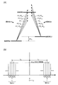
アルカリ金属原子と2つの共鳴光との相互作用機構は、図13(A)に示すように、Λ型3準位系モデルで説明できることが知られている。アルカリ金属原子は2つの基底準位を有し、基底準位1と励起準位とのエネルギー差に相当する波長(周波数f1)を有する共鳴光1、あるいは基底準位2と励起準位とのエネルギー差に相当する波長(周波数f2)を有する共鳴光2を、それぞれ単独でアルカリ金属原子に照射すると、よく知られているように光吸収が起きる。ところが、図13(B)に示すように、このアルカリ金属原子に、周波数差f1−f2が基底準位1と基底準位2のエネルギー差ΔE12に相当する周波数と正確に一致する共鳴光1と共鳴光2を同時に照射すると、2つの基底準位の重ね合わせ状態、即ち量子干渉状態になり、励起準位への励起が停止して共鳴光1と共鳴光2がアルカリ金属原子を透過する透明化現象(EIT現象)が起きる。このEIT現象を利用し、共鳴光1と共鳴光2との周波数差f1−f2が基底準位1と基底準位2のエネルギー差ΔE12に相当する周波数からずれた時の光吸収挙動の急峻な変化を検出し制御することで、高精度な発振器をつくることができる。
It is known that the interaction mechanism between an alkali metal atom and two resonance lights can be explained by a Λ-type three-level system model as shown in FIG. The alkali metal atom has two ground levels, and the
図14は、従来のCPT方式による原子発振器の一般的な構成の概略図である。図14に示すように、従来のCPT方式による原子発振器は、電流駆動回路により発生した周波数f0(=v/λ0:vは光の速度、λ0はレーザー光の中心波長)の駆動電流を、基底準位1と基底準位2のエネルギー差ΔE12に相当する周波数の1/2の変調周波数fm1で変調することにより、半導体レーザーに周波数f1=f0+fm1の共鳴光1と周波数f2=f0−fm1の共鳴光2を発生させ(図13(B))、原子セルに含まれる気体状のアルカリ金属原子にEIT現象を起こさせる。この原子発振器は、原子セルを透過した光の検出量が最大になるように電圧制御水晶発振器(VCXO:Voltage Controlled Crystal Oscillator)の発振周波数を制御し、その発振周波数をPLL(Phase Locked Loop)により逓倍率N/R(N、Rはともに正の整数)で逓倍してΔE12に相当する周波数の1/2の変調周波数fm1の信号を生成する。このような構成によれば、電圧制御水晶発振器(VCXO)は極めて安定に発振動作を継続するので、周波数安定度が極めて高い発振信号を発生させることができる。なお、ここで言う原子セルとは、気体状のアルカリ金属原子とこれを封入する容器とから構成されたものとして、以降説明をする。
FIG. 14 is a schematic diagram of a general configuration of a conventional atomic oscillator based on the CPT method. As shown in FIG. 14, the conventional CPT type atomic oscillator has a driving current of frequency f 0 (= v / λ 0 : v is the speed of light and λ 0 is the center wavelength of the laser beam) generated by the current driving circuit. Is modulated at a modulation frequency f m1 that is ½ of the frequency corresponding to the energy difference ΔE 12 between the
しかしながら、従来の原子発振器では、ΔE12に相当する周波数(例えば、セシウム原子であれば9.19263・・・GHz)の1/2の周波数と正確に一致する変調周波数fm1を直接又は高調波によって発生させるPLL等の発振器を特別に用意しなければならないため、設計の自由度が制限される。 However, in a conventional atomic oscillator, a modulation frequency f m1 that exactly matches one half of a frequency corresponding to ΔE 12 (for example, 9.19263... GHz for a cesium atom) is directly or harmonically generated. Since an oscillator such as a PLL generated by the above method must be specially prepared, the degree of freedom in design is limited.
また、変調周波数fm1がΔE12に相当する周波数の1/2の周波数と正確に一致した状態で安定するので、従来の原子発振器では、PLLの逓倍率N/Rの精度によっては電圧制御水晶発振器(VCXO)を正確に所望の周波数(公称周波数)で発振させることができない場合がある。そのため、例えば、電圧制御水晶発振器(VCXO)の発振周波数が9.999MHzであれば、公称周波数の10MHzを得るためだけに高精度の周波数変換回路が必要になり簡易な構成で実現できない場合もある(図14参照)。 In addition, since the modulation frequency f m1 is stable in a state where it exactly matches one half of the frequency corresponding to ΔE 12 , the conventional atomic oscillator has a voltage controlled crystal depending on the precision of the PLL multiplication factor N / R. In some cases, the oscillator (VCXO) cannot be oscillated at a desired frequency (nominal frequency) accurately. For this reason, for example, if the oscillation frequency of the voltage controlled crystal oscillator (VCXO) is 9.999 MHz, a high-accuracy frequency conversion circuit is required only to obtain the nominal frequency of 10 MHz, which may not be realized with a simple configuration. (See FIG. 14).
本発明は、以上のような問題点に鑑みてなされたものであり、本発明のいくつかの態様によれば、設計の自由度を向上させることにより比較的簡易な構成の原子発振器を提供することができる。 The present invention has been made in view of the above problems, and according to some aspects of the present invention, an atomic oscillator having a relatively simple configuration is provided by improving the degree of design freedom. be able to.
(1)本発明は、アルカリ金属原子に共鳴光対を照射することにより生じる電磁誘起透過現象を利用する原子発振器であって、中心周波数をf1として周波数がΔfずつ異なる複数の周波数成分を有する第1の光と、中心周波数をf2として周波数がΔfずつ異なる複数の周波数成分を有する第2の光と、を発生させる光源と、前記アルカリ金属原子を透過した前記第1の光及び前記第2の光を含む光の強度を検出する光検出手段と、前記光検出手段の検出結果に基づいて、前記第1の光の所定の周波数成分と前記第2の光の所定の周波数成分の周波数差が前記アルカリ金属原子の2つの基底準位のエネルギー差に相当する周波数に等しくなるように制御する制御手段と、を含み、前記第1の光の中心周波数f1と前記第2の光の中心周波数f2の周波数差は、前記アルカリ金属原子の2つの基底準位のエネルギー差に相当する周波数と異なる。 (1) The present invention is an atomic oscillator that uses an electromagnetically induced transmission phenomenon generated by irradiating an alkali metal atom with a resonant light pair, and has a plurality of frequency components having a center frequency f 1 and different frequencies by Δf. A light source that generates a first light and a second light having a plurality of frequency components each having a frequency different by Δf with a center frequency of f 2 , the first light transmitted through the alkali metal atom, and the first light Light detecting means for detecting the intensity of light including two lights, and the frequency of the predetermined frequency component of the first light and the predetermined frequency component of the second light based on the detection result of the light detecting means. Control means for controlling the difference to be equal to the frequency corresponding to the energy difference between the two ground levels of the alkali metal atom, and the center frequency f 1 of the first light and the second light Center frequency The frequency difference of f 2 is different from the frequency corresponding to the energy difference between the two ground levels of the alkali metal atom.
従来のCPT方式の原子発振器では、2つの共鳴光の周波数差がアルカリ金属原子の2つの基底準位のエネルギー差に相当する周波数と一致するように制御がかかるのに対して、本発明の原子発振器では、第1の光の所定の周波数成分と第2の光の所定の周波数成分の周波数差がアルカリ金属原子の2つの基底準位のエネルギー差に相当する周波数に等しくなるように制御がかかる。すなわち、第1の光の所定の周波数成分と第2の光の所定の周波数成分が2つの共鳴光になるように制御がかかる(但し、第1の光の中心周波数f1と第2の光の中心周波数f2がともに共鳴光になることはない)。 In the conventional CPT type atomic oscillator, the frequency difference between the two resonance lights is controlled so as to coincide with the frequency corresponding to the energy difference between the two ground levels of the alkali metal atom. The oscillator is controlled so that the frequency difference between the predetermined frequency component of the first light and the predetermined frequency component of the second light is equal to the frequency corresponding to the energy difference between the two ground levels of the alkali metal atom. . That is, control is performed so that the predetermined frequency component of the first light and the predetermined frequency component of the second light become two resonance lights (however, the center frequency f 1 of the first light and the second light are center frequency f 2 never both of the resonant light).
要するに、本発明の原子発振器では、第1の光の中心周波数f1以外の所定の周波数成分と第2の光の中心周波数f2以外の所定の周波数成分の対、又は、第1の光の中心周波数f1と第2の光の中心周波数f2以外の所定の周波数成分の対、又は、第1の光の中心周波数f1以外の所定の周波数成分と第2の光の中心周波数f2の対のいずれかが共鳴対になるように設計すればよい。 In short, the atomic oscillator of the present invention, a pair of predetermined frequency component other than the center frequency f 2 of the first predetermined frequency component other than the center frequency f 1 of the light and a second light, or, the first optical center frequency f 1 and a pair of predetermined frequency components other than the center frequency f 2 of the second light, or the center frequency f 2 of the predetermined frequency component other than the center frequency f 1 of the first light and the second light Any one of the pairs may be designed to be a resonance pair.
従って、本発明によれば、従来の原子発振器と比較して設計の自由度が向上し、そのため比較的簡易な構成の原子発振器を提供することができる。 Therefore, according to the present invention, the degree of freedom of design is improved as compared with the conventional atomic oscillator, and therefore an atomic oscillator having a relatively simple configuration can be provided.
(2)この原子発振器において、前記制御手段は、前記光検出手段の検出結果に基づいて、第1の変調周波数fm1を有する第1の信号を発生させる第1の変調周波数発生手段と、第2の変調周波数fm2を有する第2の信号を発生させる第2の変調周波数発生手段と、を含み、前記光源は、前記第1の信号及び前記第2の信号に基づいて所定の周波数f0の信号を変調し、f1=f0+fm1及びf2=f0−fm1、かつ、Δf=fm2となる前記第1の光及び前記第2の光を発生させるようにしてもよい。 (2) In this atomic oscillator, the control means includes first modulation frequency generation means for generating a first signal having a first modulation frequency f m1 based on a detection result of the light detection means, Second modulation frequency generating means for generating a second signal having a modulation frequency f m2 of 2, wherein the light source has a predetermined frequency f 0 based on the first signal and the second signal. The first light and the second light satisfying f 1 = f 0 + f m1 and f 2 = f 0 −f m1 and Δf = f m2 may be generated. .
本発明の原子発振器では、第1の光の所定の周波数成分(f1+j×Δf)と第2の光の所定の周波数成分(f2+k×Δf)の周波数差、すなわち、(2×fm1+(j−k)×fm2)(j,kは整数、かつ、j≠k)がアルカリ金属原子の2つの基底準位のエネルギー差に相当する周波数と一致すればよい。 In the atomic oscillator of the present invention, the frequency difference between the predetermined frequency component (f 1 + j × Δf) of the first light and the predetermined frequency component (f 2 + k × Δf) of the second light, that is, (2 × f m1 + (j−k) × f m2 ) (j and k are integers and j ≠ k) may be equal to the frequency corresponding to the energy difference between the two ground levels of the alkali metal atom.
従って、本発明によれば、直接又は簡単な分周器等を用いて所望の周波数が得られるように、上記の条件を満たす第1の変調周波数fm1と第2の変調周波数fm2を選択すれば、比較的簡易な構成の原子発振器を実現することができる。 Therefore, according to the present invention, the first modulation frequency f m1 and the second modulation frequency f m2 satisfying the above conditions are selected so that a desired frequency can be obtained directly or using a simple frequency divider or the like. Then, an atomic oscillator having a relatively simple configuration can be realized.
(3)この原子発振器において、前記第2の変調周波数発生手段は、前記第1の信号を周波数変換して前記第2の信号を発生させるようにしてもよい。 (3) In this atomic oscillator, the second modulation frequency generation means may generate the second signal by converting the frequency of the first signal.
(4)この原子発振器において、前記第2の変調周波数発生手段は、前記第1の信号から独立して前記第2の変調周波数fm2で発振するようにしてもよい。 (4) In this atomic oscillator, the second modulation frequency generation means may oscillate at the second modulation frequency fm2 independently of the first signal.
(5)この原子発振器は、前記第1の信号を周波数変換して所定の周波数の信号を発生させる周波数変換手段を含むようにしてもよい。 (5) The atomic oscillator may include frequency conversion means for frequency-converting the first signal to generate a signal having a predetermined frequency.
(6)この原子発振器において、前記制御手段は、前記光検出手段の検出結果に基づいて、第2の変調周波数fm2を有する第2の信号を発生させる第2の変調周波数発生手段と、前記第2の信号を周波数変換して第1の変調周波数fm1を有する第1の信号を発生させる第1の変調周波数発生手段と、を含み、前記光源は、前記第1の信号及び前記第2の信号に基づいて所定の周波数f0の信号を変調し、f1=f0+fm1及びf2=f0−fm1、かつ、Δf=fm2となる前記第1の光及び前記第2の光を発生させるようにしてもよい。 (6) In the atomic oscillator, the control unit generates a second signal having a second modulation frequency f m2 based on a detection result of the light detection unit, First modulation frequency generating means for generating a first signal having a first modulation frequency f m1 by frequency-converting the second signal, wherein the light source includes the first signal and the second signal based on the signal modulates a signal of a predetermined frequency f 0, f 1 = f 0 + f m1 and f 2 = f 0 -f m1, and, Δf = f m2 to become the first light and the second The light may be generated.
本発明の原子発振器では、第1の光の所定の周波数成分(f1+j×Δf)と第2の光の所定の周波数成分(f2+k×Δf)の周波数差、すなわち、(2×fm1+(j−k)×fm2)(j,kは整数、かつ、j≠k)がアルカリ金属原子の2つの基底準位のエネルギー差に相当する周波数と一致すればよい。 In the atomic oscillator of the present invention, the frequency difference between the predetermined frequency component (f 1 + j × Δf) of the first light and the predetermined frequency component (f 2 + k × Δf) of the second light, that is, (2 × f m1 + (j−k) × f m2 ) (j and k are integers and j ≠ k) may be equal to the frequency corresponding to the energy difference between the two ground levels of the alkali metal atom.
従って、本発明によれば、直接又は簡単な分周器等を用いて所望の周波数が得られるように、上記の条件を満たす第1の変調周波数fm1と第2の変調周波数fm2を選択すれば、比較的簡易な構成の原子発振器を実現することができる。 Therefore, according to the present invention, the first modulation frequency f m1 and the second modulation frequency f m2 satisfying the above conditions are selected so that a desired frequency can be obtained directly or using a simple frequency divider or the like. Then, an atomic oscillator having a relatively simple configuration can be realized.
以下、本発明の好適な実施形態について図面を用いて詳細に説明する。なお、以下に説明する実施の形態は、特許請求の範囲に記載された本発明の内容を不当に限定するものではない。また以下で説明される構成の全てが本発明の必須構成要件であるとは限らない。 DESCRIPTION OF EMBODIMENTS Hereinafter, preferred embodiments of the present invention will be described in detail with reference to the drawings. The embodiments described below do not unduly limit the contents of the present invention described in the claims. Also, not all of the configurations described below are essential constituent requirements of the present invention.
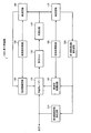
図1は、本実施形態の原子発振器の機能ブロック図である。 FIG. 1 is a functional block diagram of the atomic oscillator of this embodiment.
本実施形態の原子発振器1は、光源10、原子セル20、光検出手段30及び制御手段40を含んで構成されている。
The
光源10は、中心周波数をf1として周波数がΔfずつ異なる複数の周波数成分を有する第1の光と、中心周波数をf2として周波数がΔfずつ異なる複数の周波数成分を有する第2の光と、を発生させる。
The
原子セル20には気体状のアルカリ金属原子が含まれており、光源10により、第1の光と第2の光が照射される。以下、第1の光及び第2の光をそれぞれ「照射光1」及び「照射光2」ということにする。
The
光検出手段30は、アルカリ金属原子を透過した照射光1及び照射光2を含む光の強度を検出する。
The light detection means 30 detects the intensity of light including the
制御手段40は、光検出手段30の検出結果に基づいて、照射光1の所定の周波数成分と照射光2の所定の周波数成分の周波数差がアルカリ金属原子の2つの基底準位のエネルギー差に相当する周波数に等しくなるように制御する。ただし、本実施形態では、照射光1の中心周波数f1と照射光2の中心周波数f2の周波数差は、アルカリ金属原子の2つの基底準位のエネルギー差に相当する周波数と一致しない。
Based on the detection result of the light detection means 30, the control means 40 determines that the frequency difference between the predetermined frequency component of the
すなわち、制御手段40は、照射光1の中心周波数f1以外の所定の周波数成分と照射光2の中心周波数f2以外の所定の周波数成分の対、又は、照射光1の中心周波数f1と照射光2の中心周波数f2以外の所定の周波数成分の対、又は、照射光1の中心周波数f1以外の所定の周波数成分と照射光2の中心周波数f2の対のいずれかを共鳴光対として、その周波数がアルカリ金属原子の2つの基底準位のエネルギー差に相当する周波数と一致するように制御する。
That is, the control section 40, predetermined frequency components other than the center frequency f 1 of the
このような制御手段40は、図1に示すように、第1の変調周波数発生手段42と、第2の変調周波数発生手段44と、を含んで構成することができる。
As shown in FIG. 1, such a control unit 40 can be configured to include a first modulation
例えば、第1の変調周波数発生手段42が、光検出手段30の検出結果に基づいて、第1の変調周波数fm1を有する第1の信号を発生させ、第2の変調周波数発生手段44が、第2の変調周波数fm2を有する第2の信号を発生させるように構成してもよい。ここで、第2の変調周波数発生手段44は、第1の変調周波数発生手段42により発生する第1の信号を周波数変換して第2の信号を発生させるようにしてもよいし、第1の信号から独立して第2の変調周波数fm2で発振するように構成してもよい。後者の場合、制御手段40は、さらに、第1の信号を周波数変換して所定の周波数の信号を発生させる周波数変換手段46を含むようにしてもよい。
For example, the first modulation
また、例えば、第2の変調周波数発生手段44が、光検出手段30の検出結果に基づいて、第2の変調周波数fm2を有する第2の信号を発生させ、第1の変調周波数発生手段42が、第2の変調周波数発生手段44により発生する第2の信号を周波数変換して第1の変調周波数fm1を有する第1の信号を発生させるように構成してもよい。
Further, for example, the second modulation
そして、いずれの場合も、光源10は、第1の変調周波数発生手段42により発生する第1の信号及び第2の変調周波数発生手段44により発生する第2の信号に基づいて所定の周波数f0の信号を変調し、f1=f0+fm1及びf2=f0−fm1、かつ、Δf=fm2となる照射光1及び照射光2を発生させるようにすればよい。
In any case, the
図2(A)及び図2(B)、図3(A)及び図3(B)、図4(A)及び図4(B)は、本実施形態の原子発振器において発生する照射光1及び照射光2の第1、第2、第3の例についてそれぞれ説明するための図である。図2(A)、図3(A)及び図4(A)は、アルカリ金属原子のΛ型3準位モデルと照射光1及び照射光2の関係を示す図であり、図2(B)、図3(B)、図4(B)は、照射光1及び照射光2の周波数スペクトラムを示す図である。
2 (A) and 2 (B), FIG. 3 (A) and FIG. 3 (B), FIG. 4 (A) and FIG. 4 (B) show the
図2(B)、図3(B)及び図4(B)に示すように、第1、第2、第3の例ともに、周波数f0(=v/λ0)に対して、上側サイドバンドに周波数がfm2ずつ異なる複数の周波数成分を有する照射光1と、下側サイドバンドに周波数がfm2ずつ異なる複数の周波数成分を有する照射光2が存在する。照射光1の中心周波数f1=f0+fm1であり、照射光2の中心周波数f2=f0−fm1である。
As shown in FIGS. 2 (B), 3 (B), and 4 (B), in the first, second, and third examples, the upper side with respect to the frequency f 0 (= v / λ 0 ). frequency band with
図2(A)及び図2(B)に示すように、第1の例では、照射光1の周波数成分f1−fm2と照射光2の周波数成分f2+fm2との周波数差が、アルカリ金属原子の基底準位1と基底準位2のエネルギー差ΔE12に相当する周波数と一致している。従って、アルカリ金属原子は、照射光1の周波数成分f1−fm2と照射光2の周波数成分f2+fm2を共鳴光対としてEIT現象を起こす。
As shown in FIG. 2 (A) and FIG. 2 (B), the in the first example, the frequency difference between the
図3(A)及び図3(B)に示すように、第2の例では、照射光1の周波数成分f1+fm2と照射光2の周波数成分f2−fm2との周波数差が、アルカリ金属原子の基底準位1と基底準位2のエネルギー差ΔE12に相当する周波数と一致している。従って、アルカリ金属原子は、照射光1の周波数成分f1+fm2と照射光2の周波数成分f2−fm2を共鳴光対としてEIT現象を起こす。
As shown in FIG. 3 (A) and FIG. 3 (B), the in the second example, the frequency difference between the
図4(A)及び図4(B)に示すように、第3の例では、照射光1の中心周波数f1と照射光2の周波数成分f2+fm2との周波数差が、アルカリ金属原子の基底準位1と基底準位2のエネルギー差ΔE12に相当する周波数と一致している。従って、アルカリ金属原子は、照射光1の中心周波数f1と照射光2の周波数成分f2+fm2を共鳴光対としてEIT現象を起こす。
As shown in FIGS. 4A and 4B, in the third example, the frequency difference between the center frequency f 1 of the irradiation light 1 and the frequency component f 2 + fm 2 of the
以下、本実施形態の原子発振器のより具体的な構成について説明する。 Hereinafter, a more specific configuration of the atomic oscillator of this embodiment will be described.
(1)第1実施形態
図5は、第1実施形態の原子発振器の構成を示す図である。
(1) First Embodiment FIG. 5 is a diagram illustrating a configuration of an atomic oscillator according to a first embodiment.
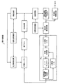
図5に示すように、第1実施形態の原子発振器100Aは、半導体レーザー110、原子セル120、光検出器130、検波回路140、低周波発振器150、電流駆動回路160、検波回路170、低周波発振器180、検波用変調回路190、第1変調周波数発生回路200、第2変調周波数発生回路210を含んで構成されている。
As shown in FIG. 5, the atomic oscillator 100A of the first embodiment includes a
原子セル120は、容器中に気体状のアルカリ金属原子(ナトリウム(Na)原子、ルビジウム(Rb)原子、セシウム(Cs)原子等)が封入されたものである。
The
この原子セル120に対して、アルカリ金属原子の2つの基底準位のエネルギー差に相当する周波数を有する共鳴光対が同時に照射されると、アルカリ金属原子がEIT現象を起こす。例えば、アルカリ金属原子がセシウム原子であれば、D1線における基底準位1と基底準位2のエネルギー差に相当する周波数が9.19263・・・GHzなので、周波数差が9.19263・・・GHzの共鳴光対が同時に照射されるとEIT現象を起こす。
When this
半導体レーザー110は、原子セル120に含まれるアルカリ金属原子に照射光1と照射光2を含むレーザー光を照射する。具体的には、半導体レーザー110が出射するレーザー光は、電流駆動回路160が出力する駆動電流によって中心周波数f0(中心波長λ0)が制御され、第1変調周波数発生回路200の出力信号(以下、「第1変調信号」という)及び第2変調周波数発生回路210の出力信号(以下、「第2変調信号」という)によって変調がかけられる。すなわち、電流駆動回路160による駆動電流に、第1変調信号の周波数成分と第2変調信号の周波数成分を有する交流電流を重畳することにより、半導体レーザー110が出射するレーザー光に変調をかけることができる。
The
なお、半導体レーザー110は、端面発光レーザー(Edge Emitting Laser)であってもよいし、垂直共振器面発光レーザー(VCSEL:Vertical Cavity Surface Emitting Laser)等の面発光レーザーであってもよい。
The
光検出器130は、原子セル120を透過した光を検出し、検出した光の量に応じた信号強度の信号を出力する。光検出器130の出力信号は検波回路140及び検波回路170に入力される。
The
検波回路140は、数Hz〜数百Hz程度の低い周波数で発振する低周波発振器150の発振信号を用いて光検出器130の出力信号を同期検波する。
The
電流駆動回路160は、検波回路140の出力信号に応じた大きさの駆動電流を発生して半導体レーザー110に供給し、レーザー光の中心周波数f0(中心波長λ0)を制御する。なお、検波回路140による同期検波を可能とするために、電流駆動回路160により発生する駆動電流には低周波発振器150の発振信号(検波回路140に供給される発振信号と同じ)が重畳される。
The
半導体レーザー110、原子セル120、光検出器130、検波回路140、電流駆動回路160を通るフィードバックループによりレーザー光の中心周波数f0(中心波長λ0)が微調整されて安定する。
The center frequency f 0 (center wavelength λ 0 ) of the laser light is finely adjusted and stabilized by a feedback loop passing through the
検波回路170は、数Hz〜数百Hz程度の低い周波数で発振する低周波発振器180の発振信号を用いて光検出器130の出力信号を同期検波する。
The
第1変調周波数発生回路200は、検波回路170の出力信号の電圧に応じた第1変調周波数fm1を有する第1変調信号を発生させる。
The first modulation
この第1変調信号は低周波発振器180の発振信号(検波回路170に供給される発振信号と同じ)で変調がかけられ、半導体レーザー110に供給される。これにより、第1変調周波数fm1をわずかにスイープさせながら検波回路170による同期検波が行われ、光検出器130の出力信号が最大になるように第1変調周波数fm1が微調整される。
This first modulation signal is modulated by the oscillation signal of the low-frequency oscillator 180 (the same as the oscillation signal supplied to the detection circuit 170) and supplied to the
第1変調信号は第2変調周波数発生回路210にも供給され、第2変調周波数発生回路210は、第1変調信号を第2変調周波数fm2を有する第2変調信号に周波数変換する。
The first modulated signal is also supplied to the second modulation
そして、半導体レーザー110が出射するレーザー光は、第1変調信号と第2変調信号により変調がかけられ、照射光1と照射光2を発生させる。
Then, the laser light emitted from the
なお、半導体レーザー110、原子セル120、光検出器130は、それぞれ図1の光源10、原子セル20、光検出手段30に対応する。また、検波回路140、低周波発振器150、電流駆動回路160、検波回路170、低周波発振器180、検波用変調回路190、第1変調周波数発生回路200、第2変調周波数発生回路210で構成される回路は、図1の制御手段40に対応する。また、第1変調周波数発生回路200、第2変調周波数発生回路210は、それぞれ図1の第1の変調周波数発生手段42、第2の変調周波数発生手段44に対応する。
The
このような構成の原子発振器100Aにおいて、半導体レーザー110が出射する照射光1の所定の周波数成分と照射光2の所定の周波数成分の周波数差が原子セル120に含まれるアルカリ金属原子の2つの基底準位のエネルギー差に相当する周波数と正確に一致しなければ、アルカリ金属原子がEIT現象を起こさないため、照射光1と照射光2の周波数に応じて光検出器130の検出量は極めて敏感に変化する。そのため、半導体レーザー110、原子セル120、光検出器130、検波回路170及び第1変調周波数発生回路200と検波用変調回路190又は第2変調周波数発生回路210を通る2つのフィードバックループにより、照射光1の所定の周波数成分と照射光2の所定の周波数成分の周波数差がアルカリ金属原子の2つの基底準位のエネルギー差に相当する周波数と極めて正確に一致するようにフィードバック制御がかかる。その結果、第1変調周波数と第2変調周波数は極めて安定した周波数になるので、第1変調信号や第2変調信号を原子発振器100Aの出力信号(クロック出力)とすることができる。
In the atomic oscillator 100A having such a configuration, the frequency difference between the predetermined frequency component of the
図6は、第1実施形態の原子発振器における照射光1及び照射光2の一例について説明するための図である。
FIG. 6 is a diagram for explaining an example of the
図6に示す照射光1と照射光2の関係は、図2(B)に示した照射光1と照射光2の関係と同じであるが、図3(B)や図4(B)に示した関係等、照射光1の所定の周波数成分と照射光2の所定の周波数成分の周波数差がアルカリ金属原子の2つの基底準位のエネルギー差ΔE12に相当する周波数と一致する(ただし、照射光1の中心周波数f1と照射光2の中心周波数f2の周波数差はΔE12に相当する周波数と一致しない)ような関係であればよい。
The relationship between the
原子発振器100Aによれば、図6に示すように、レーザー光の中心周波数f0(=v/λ0)に対して、中心周波数f1=f0+fm1であり周波数がfm2ずつ異なる照射光1の全体と、中心周波数f2=f0−fm1であり周波数がfm2ずつ異なる照射光2の全体を線対称にスイープさせながら同期検波が行われ、2×(fm1−fm2)がΔE12に相当する周波数と一致する状態で安定するようになる。
According to the atomic oscillator 100A, as shown in FIG. 6, with respect to the center frequency f 0 (= v / λ 0 ) of the laser light, the center frequency f 1 = f 0 + f m1 and the frequency is different by f m2 Synchronous detection is performed while sweeping the
アルカリ金属原子がセシウム原子であればΔE12に相当する周波数は9.19263・・・GHzであるので、例えば、fm1=4.606315・・・GHz、fm2=10MHzで安定するように設計することができる。 If the alkali metal atom is a cesium atom, the frequency corresponding to ΔE 12 is 9.19263... GHz, so that, for example, f m1 = 4.660615... GHz and f m2 = 10 MHz are designed to be stable. can do.
この場合、第1変調周波数発生回路200は、例えば、検波回路170の出力信号の大きさに応じてインダクタンス(L)やキャパシタンス(C)を調整することにより4.6GHz近傍で共振周波数を変更可能なLC共振器によって実現することができる。また、第2変調周波数発生回路210は、例えば、入力信号(第1変調信号)の周波数を(10MHz/4.606315・・・GHz)倍にダウンコンバートして出力するダイレクトディジタルシンセサイザー(DDS:Direct Digital Synthesizer)によって実現することができる。
In this case, the first modulation
図7は、原子発振器100Aにおける第2変調周波数発生回路210の構成例を示す図である。
FIG. 7 is a diagram illustrating a configuration example of the second modulation
図7に示すように、第2変調周波数発生回路210は、周波数設定部211、アドレス演算部212、波形メモリー213、D/A変換器214、ローパスフィルター215を含むダイレクトディジタルシンセサイザー(DDS)として構成されている。
As shown in FIG. 7, the second modulation
周波数設定部211は、あらかじめ設定された周波数データ(周波数変換率を決定するためのデータ)に基づいて加算値データを生成する。先の例の場合、周波数変換率は(10MHz/4.606315・・・GHz)である。
The
アドレス演算部212は、周波数設定部211が生成する加算値データを第1変調信号に同期して順次加算することにより位相角データを計算する。具体的には、アドレス演算部212は、前回の位相角データに加算値データを加算して今回の位相角データを計算し、位相角データに相当するアドレスを生成する。アドレス演算部212は、加算値データの加算処理を繰り返すpビットのアキュムレーターにより実現することができ、アキュムレーターの出力がアドレスになる。
The
波形メモリー213には、波形パターン(例えば正弦波)の位相角と振幅値の対応関係が記憶されている。具体的には、波形メモリー213には1周期分の波形パターンを一定の時間間隔(1周期/2p)でサンプリングした2p個の点の振幅値データ(デジタルデータ)がアドレス順に記憶されており、アドレス演算部が生成するアドレスで指定される領域に記憶されている振幅値データが波形メモリー213から出力される。
The
D/A変換器214は、波形メモリー213が出力する振幅値データをD/A変換する。D/A変換器214の出力信号は第1変調信号の周期毎に階段状に変化する波形であるため、ローパスフィルター215で平滑化されて第2変調信号が生成される。
The D / A converter 214 D / A converts the amplitude value data output from the
以上の構成により、第2変調周波数発生回路210(DDS)は、周波数設定部211が生成する加算値データMに対して、第1変調周波数のM/2p倍の周波数を有する第2変調信号を出力する。従って、pを十分大きくすれば、第1変調周波数をほぼ正確に(10MHz/4.606315・・・GHz)倍することができるので、極めて高い周波数精度の10MHzを有する第2変調信号を生成することができる。
With the above configuration, the second modulation frequency generation circuit 210 (DDS) has the second modulation signal having a frequency that is M / 2 p times the first modulation frequency with respect to the addition value data M generated by the
以上に説明したように、第1実施形態の原子発振器では、照射光1の所定の周波数成分(f1+j×fm2)と照射光2の所定の周波数成分(f2+k×fm2)の周波数差、すなわち、(2×fm1+(j−k)×fm2)(j,kは整数、かつ、j≠k)がアルカリ金属原子の2つの基底準位のエネルギー差に相当する周波数と一致するように制御がかかる。
As described above, in the atomic oscillator according to the first embodiment, the predetermined frequency component (f 1 + j × f m2 ) of the
従って、第1実施形態によれば、第1変調周波数fm1又は第2変調周波数fm2が所望の周波数となるように、上記の条件を満たす第1変調周波数fm1と第2変調周波数fm2を選択すればよいので、従来の原子発振器と比較して設計の自由度が向上し、そのため比較的簡易な構成の原子発振器を提供することができる。 Therefore, according to the first embodiment, as the first modulation frequency f m1 and the second modulation frequency f m2 is the desired frequency, the above conditions are satisfied first and the modulation frequency f m1 second modulation frequency f m2 Therefore, the degree of freedom of design is improved as compared with a conventional atomic oscillator, and therefore an atomic oscillator having a relatively simple configuration can be provided.
[変形例]
図8は、第1実施形態の原子発振器の変形例の構成を示す図である。図8に示すように、変形例の原子発振器100Bは、図5に示した原子発振器100Aに対して、電気光学変調器(EOM:Electro-Optic Modulator)220が追加されている。
[Modification]
FIG. 8 is a diagram showing a configuration of a modification of the atomic oscillator of the first embodiment. As shown in FIG. 8, an atomic oscillator 100 </ b> B according to a modified example is provided with an electro-optic modulator (EOM) 220 in addition to the atomic oscillator 100 </ b> A shown in FIG. 5.
図8に示すように、原子発振器100Bでは、半導体レーザー110は、第1変調周波数fm1を有する第1変調信号や第2変調周波数fm2を有する第2変調信号による変調がかけられず、電気光学変調器(EOM)220に対して周波数f0のレーザー光を出射する。
As shown in FIG. 8, in the atomic oscillator 100B, the
そして、検波用変調回路190により変調がかけられた第1変調信号は、第2変調信号とともに電気光学変調器(EOM)220に入力される。
The first modulation signal modulated by the
電気光学変調器(EOM)220は、周波数f0のレーザー光に対して第1変調信号と第2変調信号で変調をかける。その結果、電気光学変調器(EOM)220を透過して原子セル120に照射される光には、図5に示した原子発振器100Aと同様、f0を中心とする上側サイドバンドと下側サイドバンドに、中心周波数f1=f0+fm1であり周波数がfm2ずつ異なる複数の周波数成分を有する照射光1と、中心周波数f2=f0−fm1であり周波数がfm2ずつ異なる複数の周波数成分を有する照射光2がそれぞれ発生する。
The electro-optic modulator (EOM) 220 modulates the laser light having the frequency f 0 with the first modulation signal and the second modulation signal. As a result, the light transmitted through the electro-optic modulator (EOM) 220 and applied to the
図8に示す原子発振器100Bにおけるその他の構成は、図5に示した原子発振器100Aと同じであるため同じ番号を付しており、その説明を省略する。 The other configurations in the atomic oscillator 100B shown in FIG. 8 are the same as those in the atomic oscillator 100A shown in FIG.
なお、半導体レーザー110と電気光学変調器(EOM)220による構成が図1の光源10に対応する。その他の対応関係は、図5に示した原子発振器100Aと同じである。
The configuration of the
このような構成によっても、図5に示した原子発振器Aと同様の機能及び効果を有する原子発振器を実現することができる。 Even with such a configuration, an atomic oscillator having the same functions and effects as the atomic oscillator A shown in FIG. 5 can be realized.
(2)第2実施形態
図9は、第2実施形態の原子発振器の構成を示す図である。図9に示すように、第2実施形態の原子発振器100Cは、第1変調周波数発生回路300と第2変調周波数発生回路310の接続関係が、図5に示した第1実施形態の原子発振器100Aにおける第1変調周波数発生回路200と第2変調周波数発生回路210の接続関係と逆になっている。
(2) Second Embodiment FIG. 9 is a diagram illustrating a configuration of an atomic oscillator according to a second embodiment. As shown in FIG. 9, in the atomic oscillator 100C of the second embodiment, the connection relationship between the first modulation
原子発振器100Cにおいて、第2変調周波数発生回路310は、検波回路170の出力信号の電圧に応じた第2変調周波数fm2を有する第2変調信号を発生させる。
In the atomic oscillator 100C, the second modulation
この第2変調信号は低周波発振器180の発振信号(検波回路170に供給される発振信号と同じ)で変調がかけられ、半導体レーザー110に供給される。これにより、第2変調周波数fm2をわずかにスイープさせながら検波回路170による同期検波が行われ、光検出器130の出力信号が最大になるように第2変調周波数fm2が微調整される。
This second modulation signal is modulated by the oscillation signal of the low-frequency oscillator 180 (the same as the oscillation signal supplied to the detection circuit 170) and supplied to the
第2変調信号は第1変調周波数発生回路300にも供給され、第1変調周波数発生回路300は、第2変調信号を第1変調周波数fm1を有する第1変調信号に周波数変換する。
The second modulation signal is also supplied to the first modulation
そして、半導体レーザー110が出射するレーザー光は、第1変調信号と第2変調信号により変調がかけられ、照射光1と照射光2を発生させる。
Then, the laser light emitted from the
図9に示す原子発振器100Cにおけるその他の構成は、図5に示した原子発振器100Aと同じであるため同じ番号を付しており、その説明を省略する。 The other configuration of the atomic oscillator 100C shown in FIG. 9 is the same as that of the atomic oscillator 100A shown in FIG.
なお、半導体レーザー110、原子セル120、光検出器130は、それぞれ図1の光源10、原子セル20、光検出手段30に対応する。また、検波回路140、低周波発振器150、電流駆動回路160、検波回路170、低周波発振器180、検波用変調回路190、第1変調周波数発生回路300、第2変調周波数発生回路310で構成される回路は、図1の制御手段40に対応する。また、第1変調周波数発生回路300、第2変調周波数発生回路310は、それぞれ図1の第1の変調周波数発生手段42、第2の変調周波数発生手段44に対応する。
The
このような構成の原子発振器100Cにおいて、半導体レーザー110が出射する照射光1の所定の周波数成分と照射光2の所定の周波数成分の周波数差が原子セル120に含まれるアルカリ金属原子の2つの基底準位のエネルギー差に相当する周波数と正確に一致しなければ、アルカリ金属原子がEIT現象を起こさないため、照射光1と照射光2の周波数に応じて光検出器130の検出量は極めて敏感に変化する。そのため、半導体レーザー110、原子セル120、光検出器130、検波回路170及び第2変調周波数発生回路310と検波用変調回路190又は第1変調周波数発生回路300を通る2つのフィードバックループにより、照射光1の所定の周波数成分と照射光2の所定の周波数成分の周波数差がアルカリ金属原子の2つの基底準位のエネルギー差に相当する周波数と極めて正確に一致するようにフィードバック制御がかかる。その結果、第1変調周波数と第2変調周波数は極めて安定した周波数になるので、第1変調信号や第2変調信号を原子発振器100Cの出力信号(クロック出力)とすることができる。
In the atomic oscillator 100 </ b> C having such a configuration, two bases of alkali metal atoms in which the frequency difference between the predetermined frequency component of the
図10は、第2実施形態の原子発振器における照射光1及び照射光2の一例について説明するための図である。
FIG. 10 is a diagram for explaining an example of the
図10に示す照射光1と照射光2の関係は、図2(B)に示した照射光1と照射光2の関係と同じであるが、図3(B)や図4(B)に示した関係等、照射光1の所定の周波数成分と照射光2の所定の周波数成分の周波数差がアルカリ金属原子の2つの基底準位のエネルギー差ΔE12に相当する周波数と一致する(ただし、照射光1の中心周波数f1と照射光2の中心周波数f2の周波数差はΔE12に相当する周波数と一致しない)ような関係であればよい。
The relationship between the
原子発振器100Cによれば、図10に示すように、周波数がfm2ずつ異なる照射光1の各周波数成分を中心周波数f1=f0+fm1に対して線対称にスイープさせるとともに、周波数がfm2ずつ異なる照射光2の各周波数成分を中心周波数f2=f0−fm1に対して線対称にスイープさせながら同期検波が行われ、2×(fm1−fm2)がΔE12に相当する周波数と一致する状態で安定するようになる。
According to the atomic oscillator 100C, as shown in FIG. 10, the frequency components of the
アルカリ金属原子がセシウム原子であればΔE12に相当する周波数は9.19263・・・GHzであるので、例えば、fm1=4.606315・・・GHz、fm2=10MHzで安定するように設計することができる。 If the alkali metal atom is a cesium atom, the frequency corresponding to ΔE 12 is 9.19263... GHz, so that, for example, f m1 = 4.660615... GHz and f m2 = 10 MHz are designed to be stable. can do.
この場合、第2変調周波数発生回路310は、例えば、検波回路170の出力信号の大きさに応じて水晶振動子の負荷容量を調整することにより発振周波数を変更可能な電圧制御水晶発振器(VCXO:Voltage Controlled Crystal Oscillator)によって実現することができる。また、第1変調周波数発生回路300は、例えば、入力信号(第2変調信号)の周波数を(4.606315・・・GHz/10MHz)倍に逓倍するPLLによって実現することができる。
In this case, the second modulation
図11は、原子発振器100Cにおける第1変調周波数発生回路300の構成例を示す図である。
FIG. 11 is a diagram illustrating a configuration example of the first modulation
図11に示すように、第1変調周波数発生回路300は、分周器301、位相比較器302、ループフィルター303、電圧制御発振器(VCO:Voltage Controlled Oscillator)304、分周器305を含むPLLとして構成されている。
As shown in FIG. 11, the first modulation
分周器301は、第2変調信号の周波数(第2変調周波数fm2)を1/R(Rはあらかじめ決められた整数値)にして出力する。
The
位相比較器302は、分周器301の出力信号と分周器305の出力信号の位相差を電圧に変換して出力する。
The
ループフィルター303は、位相比較器302の出力電圧に含まれる高周波成分を除去(正確には一定レベル以下に減衰)する。
The
電圧制御発振器(VCO)304は、ループフィルター303の出力電圧に応じた周波数の信号を出力する。
A voltage controlled oscillator (VCO) 304 outputs a signal having a frequency corresponding to the output voltage of the
分周器305は、電圧制御発振器(VCO)304の出力周波数を1/N(Nはあらかじめ決められた整数値)にして出力する。
The
そして、電圧制御発振器(VCO)304の出力信号が第1変調信号(第1変調周波数fm1を有する)になる。 Then, the output signal of the voltage controlled oscillator (VCO) 304 becomes the first modulation signal (having the first modulation frequency f m1 ).
このような構成によれば、位相比較器302に入力される2つの信号の周波数が一致するように、すなわちfm2/R=fm1/Nとなるようにフィードバック制御がかかるので、fm1=(N/R)×fm2となる第1変調信号が得られる。
According to such a configuration, the feedback control is performed so that the frequencies of the two signals input to the
図2(A)及び図2(B)に示したような照射光1と照射光2を発生させる場合は、アルカリ金属原子がセシウム原子であれば、例えば、fm1=4.606315・・・GHz、fm2=10MHzであればよいので、逓倍率N/Rが(4.606315・・・GHz/10MHz)になるようにN及びRを決定すればよい。
When the
また、図3(A)及び図3(B)に示したような照射光1と照射光2を発生させる場合は、アルカリ金属原子がセシウム原子であれば、例えば、fm1=4.586315・・・GHz、fm2=10MHzであればよいので、逓倍率N/Rが(4.586315・・・GHz/10MHz)になるようにN及びRを決定すればよい。
Further, when the
また、図4(A)及び図4(B)に示したような照射光1と照射光2を発生させる場合は、アルカリ金属原子がセシウム原子であれば、例えば、fm1=4.601315・・・GHz、fm2=10MHzであればよいので、逓倍率N/Rが(4.601315・・・GHz/10MHz)になるようにN及びRを決定すればよい。
Further, when the
以上に説明したように、第2実施形態の原子発振器では、第1実施形態と同様に、照射光1の所定の周波数成分(f1+j×fm2)と照射光2の所定の周波数成分(f2+k×fm2)の周波数差、すなわち、(2×fm1+(j−k)×fm2)(j,kは整数、かつ、j≠k)がアルカリ金属原子の2つの基底準位のエネルギー差に相当する周波数と一致するように制御がかかる。
As described above, in the atomic oscillator of the second embodiment, the predetermined frequency component (f 1 + j × f m2 ) of the
従って、第2実施形態によれば、第1変調周波数fm1又は第2変調周波数fm2が所望の周波数となるように、上記の条件を満たす第1変調周波数fm1と第2変調周波数fm2を選択すればよいので、従来の原子発振器と比較して設計の自由度が向上し、そのため比較的簡易な構成の原子発振器を提供することができる。 Therefore, according to the second embodiment, as the first modulation frequency f m1 and the second modulation frequency f m2 is the desired frequency, the above conditions are satisfied first and the modulation frequency f m1 second modulation frequency f m2 Therefore, the degree of freedom of design is improved as compared with a conventional atomic oscillator, and therefore an atomic oscillator having a relatively simple configuration can be provided.
また、第2実施形態において、第2変調周波数fm2をMHz帯の周波数に決定すれば、第2変調周波数発生回路310や検波用変調回路190をMHz帯の回路によって実現することができるので、高度な設計技術を要するマイクロ波回路の設計を大幅に省略することができる。
In the second embodiment, if the second modulation frequency f m2 is determined to be a frequency in the MHz band, the second modulation
(3)第3実施形態
図12は、第3実施形態の原子発振器の構成を示す図である。図3に示すように、第3実施形態の原子発振器100Dは、第2変調周波数発生回路410に第1変調周波数発生回路200による第1変調信号が入力されない点において図5に示した第1実施形態の原子発振器100Aと異なる。また、第3実施形態の原子発振器100Dには周波数変換回路230が追加されている。
(3) Third Embodiment FIG. 12 is a diagram illustrating a configuration of an atomic oscillator according to a third embodiment. As shown in FIG. 3, the atomic oscillator 100 </ b> D of the third embodiment is the first implementation shown in FIG. 5 in that the first modulation signal from the first modulation
原子発振器100Dにおいて、第2変調周波数発生回路410は、第1変調周波数発生回路200により発生する第1変調信号から独立して第2変調周波数fm2を有する第2変調信号を発生させる。第2変調周波数発生回路410は、例えば、水晶振動子が周波数fm2で発振するように負荷容量が調整された水晶発振器(XO:Crystal Oscillator)によって実現することができる。
In the atomic oscillator 100D, the second modulation
そして、半導体レーザー110が出射するレーザー光は、第1変調信号と第2変調信号により変調がかけられ、照射光1と照射光2を発生させる。
Then, the laser light emitted from the
周波数変換回路230は、第1変調信号を所望の周波数の信号に周波数変換する。周波数変換回路230は、例えば、ダイレクトディジタルシンセサイザー(DDS)によって実現することができる。
The
図12に示す原子発振器100Dにおけるその他の構成は、図5に示した原子発振器100Aと同じであるため同じ番号を付しており、その説明を省略する。 The other configurations of the atomic oscillator 100D shown in FIG. 12 are the same as those of the atomic oscillator 100A shown in FIG.
なお、半導体レーザー110、原子セル120、光検出器130は、それぞれ図1の光源10、原子セル20、光検出手段30に対応する。また、検波回路140、低周波発振器150、電流駆動回路160、検波回路170、低周波発振器180、検波用変調回路190、第1変調周波数発生回路200、第2変調周波数発生回路410で構成される回路は、図1の制御手段40に対応する。また、第1変調周波数発生回路200、第2変調周波数発生回路410、周波数変換回路230は、それぞれ図1の第1の変調周波数発生手段42、第2の変調周波数発生手段44、周波数変換手段46に対応する。
The
このような構成の原子発振器100Dによれば、第2変調周波数fm2が固定されているので、アルカリ金属原子がEIT現象を起こすように第1変調周波数fm1が微調整され、第1変調周波数fm1が所望の周波数に変換されて出力される。従って、第3実施形態によれば、所望の周波数を得るために、第1変調周波数fm1、第2変調周波数fm2、周波数変換回路230の周波数変換率の組み合わせをある程度自由に選択できるので、設計の自由度を向上させることができる。
According to the atomic oscillator 100D having such a configuration, since the second modulation frequency f m2 is fixed, the first modulation frequency f m1 is finely adjusted so that the alkali metal atom causes the EIT phenomenon. f m1 is converted to a desired frequency and output. Therefore, according to the third embodiment, in order to obtain a desired frequency, the combination of the first modulation frequency f m1 , the second modulation frequency f m2 , and the frequency conversion rate of the
また、例えば、照射光1と照射光2が図2(A)及び図2(B)に示した関係にあり、アルカリ金属原子がセシウム原子である場合、第2変調信号の周波数(第2変調周波数fm2)が10MHzに対して±1kHz(±100ppm)の範囲で変動するなら、第1変調信号の周波数(第1変調周波数fm1)は4.606315・・・GHzに対して±1kHz(±1ppm未満)で変動する。従って、周波数変換回路230の周波数変換率を(10MHz/4.606315・・・GHz)に設定すれば、10MHzに対して±1ppm未満の周波数精度の出力信号が得られる。すなわち、第2変調信号の周波数精度(±100ppm)に対して、その100倍以上の周波数精度の出力信号が得られることになる。
For example, when the
このように、第3実施形態の原子発振器によれば、アルカリ金属原子のEIT現象を利用することで出力信号の周波数精度を大幅に向上させることができる。 Thus, according to the atomic oscillator of the third embodiment, the frequency accuracy of the output signal can be greatly improved by utilizing the EIT phenomenon of alkali metal atoms.
また、第3実施形態の原子発振器において、第2変調周波数発生回路410を、例えば電圧制御水晶発振器(VCXO)によって実現すれば、第2変調周波数が変更可能になり、周波数変換回路230の出力信号は第2変調周波数に応じた周波数になる。すなわち、出力周波数が可変な原子発振器を実現することができる。
Further, in the atomic oscillator of the third embodiment, if the second modulation
なお、本発明は本実施形態に限定されず、本発明の要旨の範囲内で種々の変形実施が可能である。 In addition, this invention is not limited to this embodiment, A various deformation | transformation implementation is possible within the range of the summary of this invention.
例えば、第1実施形態やその変形例の原子発振器では、第2変調周波数発生回路210は、ダイレクトディジタルシンセサイザー(DDS)によって実現しているが、PLLによって実現することもできる。
For example, in the atomic oscillator of the first embodiment or its modification, the second modulation
また、例えば、第2実施形態の原子発振器では、第1変調周波数発生回路300は、PLLによって実現しているが、逓倍機能付きのダイレクトディジタルシンセサイザー(DDS)によって実現することもできる。
Further, for example, in the atomic oscillator of the second embodiment, the first modulation
本発明は、実施の形態で説明した構成と実質的に同一の構成(例えば、機能、方法及び結果が同一の構成、あるいは目的及び効果が同一の構成)を含む。また、本発明は、実施の形態で説明した構成の本質的でない部分を置き換えた構成を含む。また、本発明は、実施の形態で説明した構成と同一の作用効果を奏する構成又は同一の目的を達成することができる構成を含む。また、本発明は、実施の形態で説明した構成に公知技術を付加した構成を含む。 The present invention includes configurations that are substantially the same as the configurations described in the embodiments (for example, configurations that have the same functions, methods, and results, or configurations that have the same objects and effects). In addition, the invention includes a configuration in which a non-essential part of the configuration described in the embodiment is replaced. In addition, the present invention includes a configuration that exhibits the same operational effects as the configuration described in the embodiment or a configuration that can achieve the same object. Further, the invention includes a configuration in which a known technique is added to the configuration described in the embodiment.
1 原子発振器、10 光源、20 原子セル、30 光検出手段、40 制御手段、42 第1の変調周波数発生手段、44 第2の変調周波数発生手段、46 周波数変換手段、100A〜100D 原子発振器、110 半導体レーザー、120 原子セル、130 光検出器、140 検波回路、150 低周波発振器、160 電流駆動回路、170 検波回路、180 低周波発振器、190 検波用変調回路、200 第1変調周波数発生回路、210 第2変調周波数発生回路、211 周波数設定部、212 アドレス演算部、213 波形メモリー、214 D/A変換器、215 ローパスフィルター、220 電気光学変調器(EOM)、230 周波数変換回路、300 第1変調周波数発生回路、301 分周器、302 位相比較器、303 ループフィルター、304 電圧制御発振器(VCO)、305 分周器、310 第2変調周波数発生回路、410 第2変調周波数発生回路
DESCRIPTION OF
Claims (7)
前記第1の光の中心周波数と前記第2の光の中心周波数との周波数差は、前記2つの基底準位のエネルギー差に相当する周波数と異なることを特徴としている原子発振器。 A first light including a plurality of frequency components and a second light including a plurality of frequency components are incident on an atom, and one of the frequency components included in the first light is included in the second light. The frequency difference with any one of the frequency components generated is equal to the frequency corresponding to the energy difference between the two ground levels of the atom, and the two frequency components are electromagnetically induced transmission phenomena based on the energy level of the three-level system. It Oko,
An atomic oscillator , wherein a frequency difference between a center frequency of the first light and a center frequency of the second light is different from a frequency corresponding to an energy difference between the two ground levels .
前記原子を収容しているセルと、
前記第1の光と前記第2の光とがそれぞれ前記セルを通過した光の強度を検出する光検出手段と、
前記光検出手段の検出結果に基づいて、前記第1の光の中心周波数および前記第2の光の中心周波数の少なくとも一方を制御する制御手段と、
を備えていることを特徴とする請求項1乃至3の何れか一項に記載の原子発振器。 A light source that generates the first light and the second light;
A cell containing the atoms;
Light detecting means for detecting the intensity of the light having passed through the cell, the first light and the second light, respectively;
Control means for controlling at least one of a center frequency of the first light and a center frequency of the second light based on a detection result of the light detection means;
The atomic oscillator according to any one of claims 1 to 3 , further comprising:
前記光源は、
前記第1の信号及び前記第2の信号に基づいて周波数f 0 の信号を変調し、中心周波数
がf 0 +f m1 であって周波数成分間の周波数差f m2 である前記第1の光及び中心周波数がf 0 −f m1 であって周波数成分間の周波数差f m2 である前記第2の光を発生させることを特徴とする請求項4に記載の原子発振器。 The control means generates first modulation frequency generation means for generating a first signal having a first modulation frequency f m1 and second modulation for generating a second signal having a second modulation frequency f m2. It has a frequency generating means,
The light source is
A signal having a frequency f 0 is modulated based on the first signal and the second signal, and a center frequency is modulated.
The second light but a frequency difference f m2 between frequency components A f 0 + f a m1 by a frequency difference f m2 between the frequency components of the first light and the center frequency f 0 -f m1 atomic oscillator according to claim 4, characterized in that to generate.
Priority Applications (5)
| Application Number | Priority Date | Filing Date | Title |
|---|---|---|---|
| JP2009258872A JP5589166B2 (en) | 2009-11-12 | 2009-11-12 | Atomic oscillator |
| US12/916,696 US8314661B2 (en) | 2009-11-12 | 2010-11-01 | Atomic oscillator |
| CN201010546843.3A CN102064828B (en) | 2009-11-12 | 2010-11-11 | Atomic oscillator |
| CN201310250110.9A CN103326720A (en) | 2009-11-12 | 2010-11-11 | Atomic oscillator |
| US13/650,787 US8760232B2 (en) | 2009-11-12 | 2012-10-12 | Atomic oscillator |
Applications Claiming Priority (1)
| Application Number | Priority Date | Filing Date | Title |
|---|---|---|---|
| JP2009258872A JP5589166B2 (en) | 2009-11-12 | 2009-11-12 | Atomic oscillator |
Publications (3)
| Publication Number | Publication Date |
|---|---|
| JP2011108678A JP2011108678A (en) | 2011-06-02 |
| JP2011108678A5 JP2011108678A5 (en) | 2012-12-20 |
| JP5589166B2 true JP5589166B2 (en) | 2014-09-17 |
Family
ID=43973722
Family Applications (1)
| Application Number | Title | Priority Date | Filing Date |
|---|---|---|---|
| JP2009258872A Active JP5589166B2 (en) | 2009-11-12 | 2009-11-12 | Atomic oscillator |
Country Status (3)
| Country | Link |
|---|---|
| US (2) | US8314661B2 (en) |
| JP (1) | JP5589166B2 (en) |
| CN (2) | CN103326720A (en) |
Families Citing this family (20)
| Publication number | Priority date | Publication date | Assignee | Title |
|---|---|---|---|---|
| US8237514B2 (en) | 2009-02-06 | 2012-08-07 | Seiko Epson Corporation | Quantum interference device, atomic oscillator, and magnetic sensor |
| JP5609130B2 (en) * | 2010-02-02 | 2014-10-22 | セイコーエプソン株式会社 | Atomic oscillator |
| JP5640490B2 (en) * | 2010-06-21 | 2014-12-17 | セイコーエプソン株式会社 | Atomic oscillator |
| JP5699467B2 (en) * | 2010-07-14 | 2015-04-08 | セイコーエプソン株式会社 | Optical module and atomic oscillator |
| JP5910808B2 (en) | 2011-03-14 | 2016-04-27 | セイコーエプソン株式会社 | Optical module and atomic oscillator for an atomic oscillator |
| JP5910807B2 (en) | 2011-03-14 | 2016-04-27 | セイコーエプソン株式会社 | Optical module and atomic oscillator for an atomic oscillator |
| JP6056118B2 (en) | 2011-03-23 | 2017-01-11 | セイコーエプソン株式会社 | Optical module and atomic oscillator |
| JP2013243329A (en) * | 2011-07-07 | 2013-12-05 | Ricoh Co Ltd | Surface emitting laser element and atomic oscillator |
| JP6303255B2 (en) * | 2011-12-02 | 2018-04-04 | 株式会社リコー | Surface emitting laser element and atomic oscillator |
| JP5874522B2 (en) * | 2012-05-09 | 2016-03-02 | セイコーエプソン株式会社 | Oscillator and electronic device |
| JP5988023B2 (en) * | 2012-05-11 | 2016-09-07 | セイコーエプソン株式会社 | Atomic oscillator control method and atomic oscillator |
| US8754697B2 (en) * | 2012-05-21 | 2014-06-17 | Raytheon Company | Hybrid dual mode frequency synthesizer circuit |
| JP6107089B2 (en) * | 2012-11-30 | 2017-04-05 | 株式会社リコー | Surface emitting laser element and atomic oscillator |
| CN103454902B (en) * | 2013-06-24 | 2015-12-09 | 苏州大学 | A kind of atomic clock |
| JP6232777B2 (en) * | 2013-06-27 | 2017-11-22 | セイコーエプソン株式会社 | Atomic oscillator, electronic device, mobile object, and GPS module |
| US9500725B2 (en) * | 2013-08-06 | 2016-11-22 | Northrop Grumman Systems Corporation | Probe beam frequency stabilization in an atomic sensor system |
| JP6519169B2 (en) * | 2014-12-19 | 2019-05-29 | セイコーエプソン株式会社 | Atomic resonance transition device, atomic oscillator, clock, electronic device and moving body |
| JP2018101877A (en) * | 2016-12-20 | 2018-06-28 | セイコーエプソン株式会社 | Atomic oscillator and electronic device |
| CN106940957B (en) * | 2017-05-15 | 2023-01-20 | 天津中德应用技术大学 | Electromagnetic induction and electromagnetic resonance comparison experimental device and experimental method thereof |
| CN114465081B (en) * | 2022-01-27 | 2023-07-21 | 清华大学 | Coupling resonance induction transparent circuit, device and laser |
Family Cites Families (10)
| Publication number | Priority date | Publication date | Assignee | Title |
|---|---|---|---|---|
| JP3305930B2 (en) * | 1995-09-14 | 2002-07-24 | 株式会社東芝 | Optical detection method and display device |
| US6320472B1 (en) * | 1999-01-26 | 2001-11-20 | Kernco, Inc. | Atomic frequency standard |
| US6762869B2 (en) * | 2002-04-09 | 2004-07-13 | California Institute Of Technology | Atomic clock based on an opto-electronic oscillator |
| US6888780B2 (en) * | 2003-04-11 | 2005-05-03 | Princeton University | Method and system for operating an atomic clock with simultaneous locking of field and frequency |
| US7378913B2 (en) * | 2003-11-26 | 2008-05-27 | Kernco, Inc. | Optically excited atomic frequency standard |
| FR2868558B1 (en) * | 2004-03-30 | 2006-06-30 | Centre Nat Rech Scient Cnrse | METHOD FOR GENERATING AN ATOMIC CLOCK SIGNAL WITH COHERENT POPULATION TRAPPING AND CORRESPONDING ATOMIC CLOCK |
| JP2009036902A (en) * | 2007-07-31 | 2009-02-19 | Nippon Telegr & Teleph Corp <Ntt> | Method and device for electromagnetically induced transparency |
| JP2009231688A (en) * | 2008-03-25 | 2009-10-08 | Epson Toyocom Corp | Optical system and atomic oscillator |
| US8237514B2 (en) * | 2009-02-06 | 2012-08-07 | Seiko Epson Corporation | Quantum interference device, atomic oscillator, and magnetic sensor |
| JP5429469B2 (en) * | 2009-09-07 | 2014-02-26 | セイコーエプソン株式会社 | Quantum interference device, atomic oscillator and magnetic sensor |
-
2009
- 2009-11-12 JP JP2009258872A patent/JP5589166B2/en active Active
-
2010
- 2010-11-01 US US12/916,696 patent/US8314661B2/en active Active
- 2010-11-11 CN CN201310250110.9A patent/CN103326720A/en active Pending
- 2010-11-11 CN CN201010546843.3A patent/CN102064828B/en active Active
-
2012
- 2012-10-12 US US13/650,787 patent/US8760232B2/en active Active
Also Published As
| Publication number | Publication date |
|---|---|
| US8760232B2 (en) | 2014-06-24 |
| CN102064828A (en) | 2011-05-18 |
| US8314661B2 (en) | 2012-11-20 |
| CN103326720A (en) | 2013-09-25 |
| US20130038398A1 (en) | 2013-02-14 |
| US20110109395A1 (en) | 2011-05-12 |
| CN102064828B (en) | 2013-07-17 |
| JP2011108678A (en) | 2011-06-02 |
Similar Documents
| Publication | Publication Date | Title |
|---|---|---|
| JP5589166B2 (en) | Atomic oscillator | |
| JP5818000B2 (en) | Atomic oscillator, control method of atomic oscillator, and quantum interference device | |
| JP5429469B2 (en) | Quantum interference device, atomic oscillator and magnetic sensor | |
| US11271575B2 (en) | Resonance generation method and atomic oscillator | |
| JP5640490B2 (en) | Atomic oscillator | |
| JP6210192B2 (en) | Atomic oscillator, method for manufacturing atomic oscillator | |
| JP5679099B2 (en) | Atomic oscillator | |
| JP2010226282A (en) | Quantum interference device and atomic oscillator | |
| JP6094730B2 (en) | Frequency conversion circuit, atomic oscillator, electronic device, and control method of frequency conversion circuit | |
| JP6142989B2 (en) | Quantum interference device, atomic oscillator, magnetic sensor, and method of manufacturing quantum interference device | |
| TW200421681A (en) | Method and apparatus for exciting resonance | |
| JP5988023B2 (en) | Atomic oscillator control method and atomic oscillator | |
| JP2015057841A (en) | Quantum interference device | |
| JP5880807B2 (en) | Coherent light source | |
| JP2005303641A (en) | Rubidium atomic oscillator | |
| JP2012049230A (en) | Quantum interference device and method of quantum interference | |
| JP2013125767A (en) | Atomic oscillator, method of controlling atomic oscillator, and quantum interference device | |
| JP6094750B2 (en) | Quantum interference device, atomic oscillator, magnetic sensor, and method of manufacturing quantum interference device | |
| JP2010199779A (en) | Atomic oscillator | |
| JP2018085591A (en) | Atomic oscillator, frequency adjustment method of atomic oscillator, and output frequency adjustment system | |
| JP5950097B2 (en) | Quantum interference device, atomic oscillator, electronic device, and quantum interference method | |
| JPH06152406A (en) | Phase synchronizing rubidium atomic oscillator | |
| JP2018101877A (en) | Atomic oscillator and electronic device | |
| JP2016152515A (en) | Atomic oscillator, method for controlling the same, and program for controlling the same | |
| JP2017188711A (en) | Quantum interference device, atomic oscillator, electronic apparatus, and movable body |
Legal Events
| Date | Code | Title | Description |
|---|---|---|---|
| A521 | Request for written amendment filed |
Free format text: JAPANESE INTERMEDIATE CODE: A523 Effective date: 20121107 |
|
| A621 | Written request for application examination |
Free format text: JAPANESE INTERMEDIATE CODE: A621 Effective date: 20121107 |
|
| A131 | Notification of reasons for refusal |
Free format text: JAPANESE INTERMEDIATE CODE: A131 Effective date: 20131225 |
|
| A521 | Request for written amendment filed |
Free format text: JAPANESE INTERMEDIATE CODE: A523 Effective date: 20140221 |
|
| TRDD | Decision of grant or rejection written | ||
| A01 | Written decision to grant a patent or to grant a registration (utility model) |
Free format text: JAPANESE INTERMEDIATE CODE: A01 Effective date: 20140604 |
|
| RD07 | Notification of extinguishment of power of attorney |
Free format text: JAPANESE INTERMEDIATE CODE: A7427 Effective date: 20140619 |
|
| A61 | First payment of annual fees (during grant procedure) |
Free format text: JAPANESE INTERMEDIATE CODE: A61 Effective date: 20140617 |
|
| R150 | Certificate of patent or registration of utility model |
Ref document number: 5589166 Country of ref document: JP Free format text: JAPANESE INTERMEDIATE CODE: R150 |
|
| S531 | Written request for registration of change of domicile |
Free format text: JAPANESE INTERMEDIATE CODE: R313531 |
|
| R350 | Written notification of registration of transfer |
Free format text: JAPANESE INTERMEDIATE CODE: R350 |