JP5910807B2 - Optical module and atomic oscillator for an atomic oscillator - Google Patents
Optical module and atomic oscillator for an atomic oscillator Download PDFInfo
- Publication number
- JP5910807B2 JP5910807B2 JP2011055433A JP2011055433A JP5910807B2 JP 5910807 B2 JP5910807 B2 JP 5910807B2 JP 2011055433 A JP2011055433 A JP 2011055433A JP 2011055433 A JP2011055433 A JP 2011055433A JP 5910807 B2 JP5910807 B2 JP 5910807B2
- Authority
- JP
- Japan
- Prior art keywords
- light
- atomic oscillator
- sideband
- optical module
- bragg grating
- Prior art date
- Legal status (The legal status is an assumption and is not a legal conclusion. Google has not performed a legal analysis and makes no representation as to the accuracy of the status listed.)
- Active
Links
- 230000003287 optical effect Effects 0.000 title claims description 50
- 150000001340 alkali metals Chemical class 0.000 claims description 31
- 239000000835 fiber Substances 0.000 claims description 26
- 229910052783 alkali metal Inorganic materials 0.000 claims description 22
- 230000000694 effects Effects 0.000 claims description 14
- 238000001514 detection method Methods 0.000 claims description 13
- 239000004065 semiconductor Substances 0.000 description 26
- 238000010586 diagram Methods 0.000 description 8
- 230000005699 Stark effect Effects 0.000 description 7
- 238000004519 manufacturing process Methods 0.000 description 7
- 239000013307 optical fiber Substances 0.000 description 5
- 230000007423 decrease Effects 0.000 description 4
- 230000007613 environmental effect Effects 0.000 description 4
- 230000000737 periodic effect Effects 0.000 description 4
- 238000001228 spectrum Methods 0.000 description 4
- 230000005284 excitation Effects 0.000 description 3
- TVFDJXOCXUVLDH-UHFFFAOYSA-N caesium atom Chemical compound [Cs] TVFDJXOCXUVLDH-UHFFFAOYSA-N 0.000 description 2
- 230000001427 coherent effect Effects 0.000 description 2
- 230000031700 light absorption Effects 0.000 description 2
- 238000012986 modification Methods 0.000 description 2
- 230000004048 modification Effects 0.000 description 2
- 239000011734 sodium Substances 0.000 description 2
- DGAQECJNVWCQMB-PUAWFVPOSA-M Ilexoside XXIX Chemical compound C[C@@H]1CC[C@@]2(CC[C@@]3(C(=CC[C@H]4[C@]3(CC[C@@H]5[C@@]4(CC[C@@H](C5(C)C)OS(=O)(=O)[O-])C)C)[C@@H]2[C@]1(C)O)C)C(=O)O[C@H]6[C@@H]([C@H]([C@@H]([C@H](O6)CO)O)O)O.[Na+] DGAQECJNVWCQMB-PUAWFVPOSA-M 0.000 description 1
- 238000010521 absorption reaction Methods 0.000 description 1
- 239000002585 base Substances 0.000 description 1
- 229910052792 caesium Inorganic materials 0.000 description 1
- 230000005686 electrostatic field Effects 0.000 description 1
- 230000003993 interaction Effects 0.000 description 1
- 229910052751 metal Inorganic materials 0.000 description 1
- 239000002184 metal Chemical group 0.000 description 1
- 239000012466 permeate Substances 0.000 description 1
- 229910052701 rubidium Inorganic materials 0.000 description 1
- IGLNJRXAVVLDKE-UHFFFAOYSA-N rubidium atom Chemical compound [Rb] IGLNJRXAVVLDKE-UHFFFAOYSA-N 0.000 description 1
- 229910052708 sodium Inorganic materials 0.000 description 1
- 239000000126 substance Substances 0.000 description 1
Images


Classifications
-
- H—ELECTRICITY
- H03—ELECTRONIC CIRCUITRY
- H03L—AUTOMATIC CONTROL, STARTING, SYNCHRONISATION OR STABILISATION OF GENERATORS OF ELECTRONIC OSCILLATIONS OR PULSES
- H03L7/00—Automatic control of frequency or phase; Synchronisation
- H03L7/26—Automatic control of frequency or phase; Synchronisation using energy levels of molecules, atoms, or subatomic particles as a frequency reference
-
- G—PHYSICS
- G04—HOROLOGY
- G04F—TIME-INTERVAL MEASURING
- G04F5/00—Apparatus for producing preselected time intervals for use as timing standards
- G04F5/14—Apparatus for producing preselected time intervals for use as timing standards using atomic clocks
- G04F5/145—Apparatus for producing preselected time intervals for use as timing standards using atomic clocks using Coherent Population Trapping
Landscapes
- Physics & Mathematics (AREA)
- Life Sciences & Earth Sciences (AREA)
- Ecology (AREA)
- General Physics & Mathematics (AREA)
- Spectroscopy & Molecular Physics (AREA)
- Stabilization Of Oscillater, Synchronisation, Frequency Synthesizers (AREA)
- Lasers (AREA)
Description
本発明は、原子発振器用の光学モジュールおよび原子発振器に関する。 The present invention relates to an optical module for an atomic oscillator and an atomic oscillator.
近年、量子干渉効果のひとつであるCPT(Coherent Population Trapping)を利用した原子発振器が提案され、装置の小型化や低消費電力化が期待されている。CPTを利用した原子発振器は、アルカリ金属原子に互いに波長(周波数)の異なる2つの共鳴光を同時に照射すると、2つの共鳴光の吸収が停止する現象(EIT現象:Electromagnetically Induced Transparency)を利用した発振器である。例えば、特許文献1には、CPTを利用した原子発振器として、コヒーレントな光を発する光源と、アルカリ金属原子が封入されたガスセルと、ガスセルを透過した光の強度を検出する受光素子と、を有する光学モジュールを含んで構成された原子発振器が記載されている。 In recent years, atomic oscillators using CPT (Coherent Population Trapping), which is one of the quantum interference effects, have been proposed, and miniaturization of devices and low power consumption are expected. An atomic oscillator using a CPT is an oscillator using a phenomenon (EIT phenomenon: Electromagnetically Induced Transparency) in which absorption of two resonance lights is stopped simultaneously when two resonance lights having different wavelengths (frequencies) are simultaneously irradiated onto an alkali metal atom. It is. For example, Patent Document 1 includes, as an atomic oscillator using CPT, a light source that emits coherent light, a gas cell in which alkali metal atoms are sealed, and a light receiving element that detects the intensity of light transmitted through the gas cell. An atomic oscillator configured to include an optical module is described.
CPTを利用した原子発振器では、例えば、光源として半導体レーザーが用いられる。光源として半導体レーザーを用いた原子発振器では、例えば、半導体レーザーの駆動電流を変調することによって半導体レーザーから出射される光に側帯波を発生させて、EIT現象を発現させている。 In an atomic oscillator using CPT, for example, a semiconductor laser is used as a light source. In an atomic oscillator using a semiconductor laser as a light source, for example, a sideband is generated in the light emitted from the semiconductor laser by modulating the driving current of the semiconductor laser, thereby causing the EIT phenomenon.
しかしながら、駆動電流が変調された半導体レーザーから出射される光には、側帯波だけでなく、EIT現象に寄与しない中心波長を有する基本波(搬送波)も含まれる。この基本波がアルカリ金属原子に照射されると、アルカリ金属原子が吸収する光の波長(周波数)が変化して(ACシュタルク効果)、原子発振器の周波数の安定度を低下させる場合がある。 However, the light emitted from the semiconductor laser whose drive current is modulated includes not only the sideband wave but also a fundamental wave (carrier wave) having a center wavelength that does not contribute to the EIT phenomenon. When the alkali metal atom is irradiated with this fundamental wave, the wavelength (frequency) of the light absorbed by the alkali metal atom changes (AC Stark effect), which may reduce the frequency stability of the atomic oscillator.
本発明のいくつかの態様に係る目的の1つは、周波数安定度の高い原子発振器を得ることが可能な原子発振器用の光学モジュールを提供することにある。また、本発明のいくつかの態様に係る目的の1つは、上記原子発振器用の光学モジュールを有する原子発振器を提供することにある。 One of the objects according to some embodiments of the present invention is to provide an optical module for an atomic oscillator capable of obtaining an atomic oscillator with high frequency stability. Another object of some aspects of the present invention is to provide an atomic oscillator having the optical module for the atomic oscillator.
本発明に係る原子発振器用の光学モジュールは、
量子干渉効果を利用する原子発振器用の光学モジュールであって、
所定の波長を有する基本波、当該基本波の側帯波、を含む光を出射する光源と、
前記光源からの光が入射し、当該入射した光のうち前記側帯波を透過させる波長選択部と、
アルカリ金属ガスを封入し、前記波長選択部を透過した光が照射されるガスセルと、
前記ガスセルに照射された光のうち前記ガスセルを透過した光の強度を検出する光検出部と、
を含み、
前記波長選択部は、
ファイバーブラッググレーティングと、
前記ファイバーブラッググレーティングに電圧を印加する電圧印加部と、
を有する。
An optical module for an atomic oscillator according to the present invention,
An optical module for an atomic oscillator using the quantum interference effect,
A light source that emits light including a fundamental wave having a predetermined wavelength, and a sideband of the fundamental wave;
A wavelength selection unit that receives light from the light source and transmits the sideband of the incident light;
A gas cell in which an alkali metal gas is sealed and irradiated with light transmitted through the wavelength selection unit;
A light detector for detecting the intensity of light transmitted through the gas cell among the light irradiated to the gas cell;
Including
The wavelength selector is
With fiber Bragg grating,
A voltage application unit for applying a voltage to the fiber Bragg grating;
Have
このような原子発振器用の光学モジュールによれば、波長選択部が、光源からの光に含まれる基本波の強度を減少または基本波を消滅させることができる。これにより、EIT現象に寄与しない基本波がアルカリ金属原子に照射されることを抑制または防止できる。したがって、ACシュタルク効果による周波数変動を抑制することができ、周波数安定度の高い発振器を提供できる。さらに、波長選択部が、ファイバーブラッググレーティングに電圧を印加するための電圧印加部を有しているため、電気光学効果によってファイバーブラッググレーティングの波長選択特性(ファイバーブラッググレーティングが選択する波長範囲)を変化させることができる。これにより、波長選択部は、製造誤差や環境変化等によるファイバーブラッググレーティングの波長選択特性のずれを補正することができる。 According to such an optical module for an atomic oscillator, the wavelength selection unit can reduce the intensity of the fundamental wave included in the light from the light source or eliminate the fundamental wave. Thereby, it can suppress or prevent that the fundamental wave which does not contribute to an EIT phenomenon is irradiated to an alkali metal atom. Therefore, frequency fluctuation due to the AC Stark effect can be suppressed, and an oscillator with high frequency stability can be provided. Furthermore, since the wavelength selection unit has a voltage application unit for applying voltage to the fiber Bragg grating, the wavelength selection characteristics of the fiber Bragg grating (wavelength range selected by the fiber Bragg grating) are changed by the electro-optic effect Can be made. Thereby, the wavelength selection part can correct | amend the shift | offset | difference of the wavelength selection characteristic of a fiber Bragg grating by a manufacturing error, an environmental change, etc.
本発明に係る原子発振器用の光学モジュールにおいて、
前記電圧印加部は、第1電極および第2電極を有し、
前記ファイバーブラッググレーティングは、前記第1電極と前記第2電極の間に配置されていることができる。
In the optical module for an atomic oscillator according to the present invention,
The voltage application unit includes a first electrode and a second electrode,
The fiber Bragg grating may be disposed between the first electrode and the second electrode.
このような原子発振器用の光学モジュールによれば、波長選択部を簡易な構成とすることができる。 According to such an optical module for an atomic oscillator, the wavelength selection unit can have a simple configuration.
本発明に係る原子発振器用の光学モジュールにおいて、
前記光源は、面発光型レーザーであることができる。
In the optical module for an atomic oscillator according to the present invention,
The light source may be a surface emitting laser.
このような原子発振器用の光学モジュールによれば、面発光型レーザーは、端面発光型レーザーと比べて、ゲインを生じさせるための電流が少ないため、低消費電力化を図ることができる。 According to such an optical module for an atomic oscillator, the surface-emitting laser has a smaller current for generating a gain than the edge-emitting laser, so that the power consumption can be reduced.
本発明に係る原子発振器用の光学モジュールにおいて、
さらに、前記光源から出射された光を、前記ファイバーブラッググレーティングに入射させる光学素子を有することができる。
In the optical module for an atomic oscillator according to the present invention,
Furthermore, the optical element which makes the light radiate | emitted from the said light source inject into the said fiber Bragg grating can be provided.
このような原子発振器用の光学モジュールによれば、光源から出射された光を、効率よくファイバーブラッググレーティングに導くことができる。 According to such an optical module for an atomic oscillator, light emitted from the light source can be efficiently guided to the fiber Bragg grating.
本発明に係る原子発振器は、
本発明に係る原子発振器用の光学モジュールを含む。
The atomic oscillator according to the present invention is
An optical module for an atomic oscillator according to the present invention is included.
このような原子発振器は、本発明に係る原子発振器用の光学モジュールを含むため、ACシュタルク効果による周波数変動を抑制することができ、周波数安定度を高めることができる。 Since such an atomic oscillator includes the optical module for an atomic oscillator according to the present invention, frequency fluctuation due to the AC Stark effect can be suppressed and frequency stability can be increased.
本発明に係る原子発振器は、
量子干渉効果を利用する原子発振器であって、
所定の波長を有する基本波、当該基本波の側帯波、を含む光を出射する光源と、
前記光源からの光が入射し、当該入射した光のうち前記側帯波を透過させる波長選択部と、
アルカリ金属ガスを封入し、前記波長選択部を透過した光が照射されるガスセルと、
前記ガスセルに照射された光のうち前記ガスセルを透過した光の強度を検出する光検出部と、
を含み、
前記波長選択部は、
ファイバーブラッググレーティングと、
前記ファイバーブラッググレーティングに電圧を印加する電圧印加部と、
を有する。
The atomic oscillator according to the present invention is
An atomic oscillator that uses the quantum interference effect,
A light source that emits light including a fundamental wave having a predetermined wavelength, and a sideband of the fundamental wave;
A wavelength selection unit that receives light from the light source and transmits the sideband of the incident light;
A gas cell in which an alkali metal gas is sealed and irradiated with light transmitted through the wavelength selection unit;
A light detector for detecting the intensity of light transmitted through the gas cell among the light irradiated to the gas cell;
Including
The wavelength selector is
With fiber Bragg grating,
A voltage application unit for applying a voltage to the fiber Bragg grating;
Have
このような原子発振器によれば、波長選択部が、光源からの光に含まれる基本波の強度を減少または基本波を消滅させることができる。これにより、EIT現象に寄与しない基本波がアルカリ金属原子に照射されることを抑制または防止できる。したがって、ACシュタルク効果による周波数変動を抑制することができ、周波数安定度の高い発振器を提供できる。さらに、波長選択部が、ファイバーブラッググレーティングに電圧を印加するための電圧印加部を有しているため、電気光学効果によってファイバーグレーティングの波長選択特性(ファイバーブラッググレーティングが選択する波長範囲)を変化させることができる。これにより、波長選択部は、製造誤差や環境変化等によるファイバーブラッググレーティングの波長選択特性のずれを補正することができる。 According to such an atomic oscillator, the wavelength selection unit can reduce the intensity of the fundamental wave included in the light from the light source or eliminate the fundamental wave. Thereby, it can suppress or prevent that the fundamental wave which does not contribute to an EIT phenomenon is irradiated to an alkali metal atom. Therefore, frequency fluctuation due to the AC Stark effect can be suppressed, and an oscillator with high frequency stability can be provided. Further, since the wavelength selection unit has a voltage application unit for applying a voltage to the fiber Bragg grating, the wavelength selection characteristic of the fiber grating (the wavelength range selected by the fiber Bragg grating) is changed by the electro-optic effect. be able to. Thereby, the wavelength selection part can correct | amend the shift | offset | difference of the wavelength selection characteristic of a fiber Bragg grating by a manufacturing error, an environmental change, etc.
以下、本発明の好適な実施形態について、図面を参照しながら説明する。 Preferred embodiments of the present invention will be described below with reference to the drawings.
まず、本実施形態に係る光学モジュールおよび原子発振器について、図面を参照しながら説明する。本実施形態に係る原子発振器は、本実施形態に係る光学モジュールを含む。図1は、本実施形態に係る原子発振器1の機能ブロック図である。原子発振器1は、量子干渉効果を利用した発振器である。 First, an optical module and an atomic oscillator according to this embodiment will be described with reference to the drawings. The atomic oscillator according to the present embodiment includes the optical module according to the present embodiment. FIG. 1 is a functional block diagram of an atomic oscillator 1 according to this embodiment. The atomic oscillator 1 is an oscillator using a quantum interference effect.
原子発振器1は、光学モジュール2と、制御部50と、を含む。
The atomic oscillator 1 includes an optical module 2 and a
光学モジュール2は、光源10と、波長選択部20と、ガスセル30と、光検出部40と、を含む。
The optical module 2 includes a
光源10は、所定の中心波長(中心周波数)を有する基本波Fと、互いに異なる波長を有する第1側帯波W1および第2側帯波W2と、を含む第1光L1を発生させる。
The
波長選択部20は、第1光L1から第1側帯波W1および第2側帯波W2を選択し、第2光L2として射出する。波長選択部20は、所定の波長範囲の光を選択して射出するファイバーブラッググレーティング(以下、「FBG」ともいう)20aと、FBG20aに電圧を印加するための電圧印加部20bと、を有する。電圧印加部20bは、FBG20aに電圧を印加することにより、FBG20aが選択する波長範囲(波長選択特性)を変化させることができる。
The
ガスセル30は、アルカリ金属ガスを封入しており、ガスセル30には、第2光L2が照射される。
The
光検出部40は、ガスセル30を透過した第2光L2の強度を検出する。
The
制御部50は、光検出部40の検出結果に基づいて、第1側帯波W1および第2側帯波W2の波長(周波数)差が、ガスセル30に封入されたアルカリ金属原子の2つの基底準位のエネルギー差に相当する周波数に等しくなるように制御する。制御部50は、光検出部40の検出結果に基づいて、変調周波数fmを有する検出信号を発生させる。そして、光源10は、この検出信号に基づいて所定の周波数f0を有する基本波Fを変調して、周波数f1=f0+fmを有する第1側帯波W1、および周波数f2=f0−fmを有する第2側帯波W2を発生させる。
Based on the detection result of the
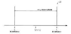
図2(A)は、アルカリ金属原子のΛ型3準位モデルと第1側帯波W1及び第2側帯波W2の関係を示す図である。図2(B)は、光源10で発生する第1光L1の周波数スペクトラムを示す図である。
FIG. 2A is a diagram showing the relationship between the Λ-type three-level model of alkali metal atoms and the first sideband wave W1 and the second sideband wave W2. FIG. 2B is a diagram showing a frequency spectrum of the first light L1 generated by the
図2(B)に示すように、光源10において発生する第1光L1は、中心周波数f0(=v/λ0:vは光の速度、λ0はレーザー光の中心波長)を有する基本波Fと、中心周波数f0に対して上側サイドバンドに周波数f1を有する第1側帯波W1と、中心周波数f0に対して下側サイドバンドに周波数f2を有する第2側帯波W2と、を含む。第1側帯波W1の周波数f1は、f1=f0+fmであり、第2側帯波W2の周波数f2は、f2=f0−fmである。
As shown in FIG. 2B, the first light L1 generated in the
図2(A)及び図2(B)に示すように、第1側帯波W1の周波数f1と第2側帯波W2の周波数f2との周波数差が、アルカリ金属原子の基底準位GL1と基底準位GL2のエネルギー差ΔE12に相当する周波数と一致している。したがって、アルカリ金属原子は、周波数f1を有する第1側帯波W1と周波数f2を有する第2側帯波W2によってEIT現象を起こす。 As shown in FIG. 2 (A) and FIG. 2 (B), the frequency difference between the frequency f 2 of the frequency f 1 and the second sideband wave W2 of the first sideband W1 is a ground level GL1 alkali metal atom It coincides with the frequency corresponding to the energy difference Delta] E 12 ground levels GL2. Thus, alkali metal atom, causes EIT phenomenon by the second sideband wave W2 having a first sideband wave W1 and the frequency f 2 having a frequency f 1.
ここで、EIT現象について説明する。アルカリ金属原子と光との相互作用は、Λ型3準位系モデルで説明できることが知られている。図2(A)に示すように、アルカリ金属原子は2つの基底準位を有し、基底準位GL1と励起準位とのエネルギー差に相当する波長(周波数f1)を有する第1側帯波W1、あるいは基底準位GL2と励起準位とのエネルギー差に相当する波長(周波数f2)を有する第2側帯波W2を、それぞれ単独でアルカリ金属原子に照射すると、光吸収が起きる。ところが、図2(B)に示すように、このアルカリ金属原子に、周波数差f1−f2が基底準位GL1と基底準位GL2のエネルギー差ΔE12に相当する周波数と正確に一致する第1側帯波W1と第2側帯波W2を同時に照射すると、2つの基底準位の重ね合わせ状態、即ち量子干渉状態になり、励起準位への励起が停止して第1側帯波W1と第2側帯波W2がアルカリ金属原子を透過する透明化現象(EIT現象)が起きる。このEIT現象を利用し、第1側帯波W1と第2側帯波W2との周波数差f1−f2が基底準位GL1と基底準位GL2のエネルギー差ΔE12に相当する周波数からずれた時の光吸収挙動の急峻な変化を検出し制御することで、高精度な発振器をつくることができる。 Here, the EIT phenomenon will be described. It is known that the interaction between alkali metal atoms and light can be explained by a Λ-type three-level model. As shown in FIG. 2A, the alkali metal atom has two ground levels, and a first sideband having a wavelength (frequency f 1 ) corresponding to the energy difference between the ground level GL1 and the excited level. When an alkali metal atom is irradiated with W1 or a second sideband wave W2 having a wavelength (frequency f 2 ) corresponding to the energy difference between the ground level GL2 and the excitation level, light absorption occurs. However, as shown in FIG. 2B, the frequency difference f 1 -f 2 exactly matches the frequency corresponding to the energy difference ΔE 12 between the ground level GL 1 and the ground level GL 2. When the first sideband wave W1 and the second sideband wave W2 are irradiated at the same time, the two base levels are superposed, that is, a quantum interference state, and the excitation to the excitation level is stopped and the first sideband wave W1 and the second sideband wave W2 A transparency phenomenon (EIT phenomenon) in which the sideband wave W2 passes through the alkali metal atom occurs. When the EIT phenomenon utilizing a frequency difference f 1 -f 2 between the first sideband wave W1 and the second sideband wave W2 is shifted from the frequency corresponding to the energy difference Delta] E 12 ground levels GL1 and ground level GL2 By detecting and controlling a steep change in the light absorption behavior of the laser, a highly accurate oscillator can be produced.
しかし、図2(B)に示した第1光L1がガスセル30に直接照射されると、第1側帯波W1と第2側帯波W2と同時に、基本波Fがガスセル30すなわちアルカリ金属原子に照射されることになる。EIT現象に寄与しない基本波Fがアルカリ金属原子に照射されると、ACシュタルク効果により、アルカリ金属原子が吸収する光の波長(周波数)が変化する。これにより、アルカリ金属原子を透過する第1側帯波W1と第2側帯波W2の量が変化してしまう。EIT現象を利用した発振器においては、アルカリ金属原子を透過する第1側帯波W1と第2側帯波W2の量を検知することで変調周波数fmを安定化させ、この変調周波数fmを発信器の出力として利用することにより、発信器の周波数安定度を高めている。従って、基本波Fによって生じるACシュタルク効果は、第1側帯波W1と第2側帯波W2の検知精度を低下させ、変調周波数fmの安定度を低下させる。すなわち、発信器の周波数安定度を低下させてしまう。
However, when the first light L1 shown in FIG. 2B is directly applied to the
図3は、波長選択部20から射出された第2光L2の周波数スペクトラムを示す図である。
FIG. 3 is a diagram illustrating a frequency spectrum of the second light L2 emitted from the
第2光L2は、第1光L1と比べて、基本波Fが消滅または基本波Fの強度が減少した光である。図3の例では、第2光L2は、中心周波数f0に対して上側サイドバンドに周波数f1を有する第1側帯波W1、および中心周波数f0に対して下側サイドバンドに周波数f2を有する第2側帯波W2のみを有している。このように、光学モジュール2では、波長選択部20によって、基本波Fの強度を減少または基本波Fを消滅させることができる。
The second light L2 is light in which the fundamental wave F disappears or the intensity of the fundamental wave F decreases compared to the first light L1. FIG The third example, the second light L2, the center frequency the first sideband having a frequency f 1 to the upper sideband with respect to f 0 W1, and the center frequency f 2 to the lower sideband with respect to the frequency f 0 Only the second sideband W2 having Thus, in the optical module 2, the
以下、本実施形態の原子発振器のより具体的な構成について説明する。 Hereinafter, a more specific configuration of the atomic oscillator of this embodiment will be described.
図4は、原子発振器1の構成を示すブロック図である。 FIG. 4 is a block diagram showing the configuration of the atomic oscillator 1.
原子発振器1は、図4に示すように、光学モジュール2と、電流駆動回路150と、変調回路160と、を含む。
As shown in FIG. 4, the atomic oscillator 1 includes an optical module 2, a
光学モジュール2は、半導体レーザー110と、波長選択装置120と、ガスセル130と、光検出器140と、を含む。
The optical module 2 includes a
半導体レーザー110は、所定の中心波長を有する基本波Fと、互いに異なる波長を有する第1側帯波W1および第2側帯波W2と、を含む第1光L1を発生させる。半導体レーザー110が出射するレーザー光(第1光L1)は、電流駆動回路150が出力する駆動電流によって中心周波数f0(中心波長λ0)が制御され、変調回路160の出力信号(変調信号)によって変調がかけられる。すなわち、電流駆動回路150による駆動電流に、変調信号の周波数成分を有する交流電流を重畳することにより、半導体レーザー110が出射する第1光L1に変調をかけることができる。これにより、第1光L1には、第1側帯波W1、および第2側帯波W2が生成される。半導体レーザー110において発生する光は、可干渉性を有するため、量子干渉効果を得るために好適である。
The
図2(B)に示すように、第1光L1は、中心周波数f0(=v/λ0:vは光の速度、λ0は第1光L1の中心波長)を有する基本波Fと、中心周波数f0に対して上側サイドバンドに周波数f1を有する第1側帯波W1と、中心周波数f0に対して下側サイドバンドに周波数f2を有する第2側帯波W2と、を含む。第1側帯波W1の周波数f1は、f1=f0+fmであり、第2側帯波W2の周波数f2は、f2=f0−fmである。 As shown in FIG. 2B, the first light L1 includes a fundamental wave F having a center frequency f 0 (= v / λ 0 : v is the speed of light, and λ 0 is the center wavelength of the first light L1). includes a first sideband W1 having a frequency f 1 to the upper sideband with respect to the center frequency f 0, and the second sideband wave W2 having a frequency f 2 to the lower sideband with respect to the center frequency f 0, the . Frequency f 1 of the first sideband W1 is f 1 = f 0 + f m , the frequency f 2 of the second sideband wave W2 is f 2 = f 0 -f m.
波長選択装置120は、第1光L1から第1側帯波W1および第2側帯波W2を選択し、第2光L2として射出する。波長選択装置120は、所定の波長範囲の光を選択して射出するFBG120aと、FBG120aに電圧を印加するための電圧印加装置120bと、を有する。
The
FBG120aは、第1光から第1側帯波W1および第2側帯波W2を選択して射出することができる。これにより、FBG120aに入射した第1光L1の基本波Fの強度を減少または基本波Fを消滅させて、第2光L2として射出することができる。すなわち、第2光L2では、第1光L1と比べて、基本波Fの強度が減少または基本波Fが消滅している。図3の例では、第2光L2は、第1側帯波W1および第2側帯波W2のみを有している。
The
電圧印加装置120bは、電気光学効果によって、FBG120aが選択する波長範囲(波長選択特性)を変化させることができる。ここで、電気光学効果とは、物質の光に対する屈折率が、外部より静電場を加えることによって変化する現象をいう。具体的には、電圧印加装置120bは、FBG120aに電圧を印加することにより、FBG120aの屈折率を変化させ、FBG120aの波長選択特性を制御する。波長選択装置120は、電圧印加装置120bによって、製造誤差や環境変化(熱、光など)等によるFBG120aの波長選択特性のずれを補正することができるため、第1光L1から第1側帯波W1および第2側帯波W2を、精度よく選択して射出することができる。
The
電圧印加装置120bは、光検出器140の出力信号に基づいて、FBG120aに印加する電圧の強度を調整し、FBG120aの波長選択特性を制御してもよい。光モジュール2では、例えば、FBG120a、ガスセル130、光検出器140、電圧印加装置120bを通るフィードバックループによりFBG120aに印加する電圧の強度が調整され、FBG120aの波長選択特性が制御される。
The
また、電圧印加装置120bは、予め取得されたFBG120aの波長選択特性のずれのデータに基づいて、FBG120aに印加する電圧の強度を調整し、FBG120aの波長選択特性のずれを補正してもよい。
Further, the
ガスセル130は、容器中に気体状のアルカリ金属原子(ナトリウム(Na)原子、ルビジウム(Rb)原子、セシウム(Cs)原子等)が封入されたものである。ガスセル130には、波長選択装置120から射出された第2光L2が照射される。
The
このガスセル130に対して、アルカリ金属原子の2つの基底準位のエネルギー差に相当する周波数(波長)差を有する2つの光波(第1側帯波および第2側帯波)が照射されると、アルカリ金属原子がEIT現象を起こす。例えば、アルカリ金属原子がセシウム原子であれば、D1線における基底準位GL1と基底準位GL2のエネルギー差に相当する周波数が9.19263・・・GHzなので、周波数差が9.19263・・・GHzの2つの光波が照射されるとEIT現象を起こす。
When the
光検出器140は、ガスセル130を透過した第2光L2を検出し、検出した光の量に応じた信号強度の信号を出力する。光検出器140の出力信号は、電流駆動回路150および変調回路160に入力される。また、光検出器140の出力信号は、さらに、電圧印加装置120bに入力されてもよい。光検出器140は、例えば、フォトダイオードである。
The
電流駆動回路150は、光検出器140の出力信号に応じた大きさの駆動電流を発生させて半導体レーザー110に供給し、第1光L1の中心周波数f0(中心波長λ0)を制御する。半導体レーザー110、波長選択装置120、ガスセル130、光検出器140、電流駆動回路150を通るフィードバックループにより第1光の中心周波数f0(中心波長λ0)が微調整されて安定する。
The
変調回路160は、光検出器140の出力信号に応じた変調周波数fmを有する変調信号を発生させる。この変調信号は、光検出器140の出力信号が最大になるように変調周波数fmが微調整されながら半導体レーザー110に供給される。半導体レーザー110が出射するレーザー光は、変調信号により変調がかけられ、第1側帯波W1と第2側帯波W2を発生させる。
なお、半導体レーザー110、波長選択装置120、ガスセル130、光検出器140は、それぞれ図1の光源10、波長選択部20、ガスセル30、光検出部40に対応する。また、FBG120aは、図1のFBG20aに対応し、電圧印加装置120bは、図1の電圧印加部20bに対応する。また、電流駆動回路150、変調回路160は、図1の制御部50に対応する。
The
このような構成の原子発振器1において、半導体レーザー110が発生させる第1光L1の第1側帯波W1と第2側帯波W2の周波数差がガスセル130に含まれるアルカリ金属原子の2つの基底準位のエネルギー差に相当する周波数と正確に一致しなければ、アルカリ金属原子がEIT現象を起こさないため、第1側帯波W1と照射光W2の周波数に応じて光検出器140の検出量は極めて敏感に変化する(検出量が増加する)。そのため、半導体レーザー110、波長選択装置120、ガスセル130、光検出器140、および変調回路160を通るフィードバックループにより、第1側帯波W1と第2側帯波W2との周波数差がアルカリ金属原子の2つの基底準位のエネルギー差に相当する周波数と極めて正確に一致するようにフィードバック制御がかかる。その結果、変調周波数は極めて安定した周波数になるので、変調信号を原子発振器1の出力信号(クロック出力)とすることができる。
In the atomic oscillator 1 having such a configuration, the frequency difference between the first sideband wave W1 and the second sideband wave W2 of the first light L1 generated by the
図5は、光学モジュール2の要部(半導体レーザー110および波長選択装置120)を模式的に示す斜視図である。
FIG. 5 is a perspective view schematically showing main parts (
半導体レーザー110としては、例えば、面発光型レーザーを用いることができる。面発光型レーザーは、端面発光型レーザーと比べて、ゲインを生じさせるための電流が少ないため、低消費電力化を図ることができる。なお、半導体レーザー110として、端面発光型レーザーを用いてもよい。半導体レーザー110から出射された光L1は、図5に示すように、光学素子170によって集光され、FBG120aに入射する。光学素子170は、図示の例では、半導体レーザー110から出射される光L1を集光して、FBG120aに入射させるためのレンズである。
As the
FBG120aは、光ファイバーのコアに周期的な屈折率変化を与えたものである。そのため、光ファイバーの長手方向に周期的な屈折率変調が得られ、周期に合致した波長範囲の光信号(基本波F)は反射され、他の波長範囲の光信号(第1側帯波W1および第2側帯波W2)は、この周期的な屈折率変動を感知せずに通過する。すなわち、FBG120aでは、第1側帯波W1および第2側帯波W2に対する反射率が小さく、基本波Fに対する反射率が大きい。したがって、FBG120aは、基本波Fを反射させ、第1側帯波W1および第2側帯波W2を透過させることができる。FBG120aは、光ファイバーを用いているため、変形が容易であり、設計の自由度を向上できる。FBG120aは、例えば、ボビン(図示しない)に巻き付けられていてもよい。
The
FBG120aは、図5に示すように、電圧印加装置120bの第1電極121と第2電極122との間に配置されている。FBG120aは、入射した第1光L1から第1側帯波W1および第2側帯波W2を選択して透過させることができる。
As shown in FIG. 5, the
電圧印加装置120bは、FBG120aに電圧を印加するための第1電極121および第2電極122を有している。電圧印加装置120bが、電極121,122間に位置するFBG120aに電圧を印加すると、電気光学効果が生じてFBG120aの屈折率が変化し、FBG120aの波長選択特性(FBGが選択する波長範囲)が変化する。
The
光学モジュール2および原子発振器1は、例えば、以下の特徴を有する。 The optical module 2 and the atomic oscillator 1 have the following features, for example.
光学モジュール2によれば、波長選択装置120が、第1光L1の基本波Fの強度を減少または基本波Fを消滅させることができる。これにより、EIT現象に寄与しない基本波Fがアルカリ金属原子に照射されることを抑制または防止できる。したがって、ACシュタルク効果による周波数変動を抑制することができ、周波数安定度の高い発振器を提供できる。
According to the optical module 2, the
光学モジュール2によれば、波長選択装置120が、FBG120aの選択する波長範囲を変化させる電圧印加装置120bを有しているため、製造誤差や環境変化(熱、光など)によるFBG120aの波長選択特性(FBGが選択する波長範囲)のずれを補正することができる。したがって、波長選択装置120は、第1光L1から第1側帯波W1および第2側帯波W2を、精度よく選択して射出することができる。
According to the optical module 2, since the
FBG120aの波長選択特性は、光ファイバーのコアに与えられた周期的な屈折率変化に依存する。FBG120aの製造工程において、光ファイバーのコアに周期的な屈折率変化を精度よく与えることは困難であり、FBG120aに製造誤差が生じる場合がある。このような場合であっても、波長選択装置120は、電圧印加装置120bを有するため、この製造誤差に起因する波長選択特性のずれを補正することができる。
The wavelength selection characteristic of the
光学モジュール2では、電圧印加装置120bが、電気光学効果によって、FBG120aの波長選択特性を変化させることができる。これにより、FBGの波長選択特性を、高精度かつ容易に制御できる。さらに、電圧印加装置120bは、FBG120aに電圧を印加するための第1電極121および第2電極122を含んで構成されている。したがって、波長選択装置120を簡易な構成とすることができる。
In the optical module 2, the
光学モジュール2では、半導体レーザー110が面発光型レーザーであることができる。面発光型レーザーは、端面発光型レーザーと比べて、ゲインを生じさせるための電流が少ないため、低消費電力化を図ることができる。
In the optical module 2, the
光学モジュール2では、半導体レーザー110から出射された光L1をFBG120aに入射させるための光学素子170を有する。これにより、半導体レーザー110で発生した光L1を、効率よくFBG120aに導くことができる。
The optical module 2 includes an
原子発振器1では、光学モジュール2を有している。したがって、上述のように、周波数安定度の高めることができる。 The atomic oscillator 1 has an optical module 2. Therefore, as described above, the frequency stability can be increased.
上記のように、本発明の実施形態について詳細に説明したが、本発明の新規事項および効果から実体的に逸脱しない多くの変形が可能であることは当業者には容易に理解できよう。従って、このような変形例はすべて本発明の範囲に含まれるものとする。 Although the embodiments of the present invention have been described in detail as described above, those skilled in the art will readily understand that many modifications are possible without substantially departing from the novel matters and effects of the present invention. Accordingly, all such modifications are intended to be included in the scope of the present invention.
1 原子発振器、2 光学モジュール、10 光源、20 波長選択部、
20a ファイバーブラッググレーティング、20b 電圧印加部、
30 ガスセル、40 光検出部、50 制御部、110 半導体レーザー、
120 波長選択装置、120a ファイバーブラッググレーティング、
120b 電圧印加装置、121 第1電極、122 第2電極、130 ガスセル、
140 光検出器、150 電流駆動回路、160 変調回路、170 光学素子
1 atomic oscillator, 2 optical module, 10 light source, 20 wavelength selector,
20a Fiber Bragg grating, 20b Voltage application unit,
30 gas cell, 40 light detector, 50 controller, 110 semiconductor laser,
120 wavelength selection device, 120a fiber Bragg grating,
120b voltage application device, 121 first electrode, 122 second electrode, 130 gas cell,
140 photodetector, 150 current drive circuit, 160 modulation circuit, 170 optical element
Claims (5)
所定の波長を有する基本波、当該基本波の側帯波、を含む光を出射する光源と、
前記光源からの光が入射し、当該入射した光のうち前記側帯波を透過させる波長選択部と、
アルカリ金属ガスを封入し、前記波長選択部を透過した光が照射されるガスセルと、
前記ガスセルに照射された光のうち前記ガスセルを透過した光の強度を検出する光検出部と、
を含み、
前記波長選択部は、
ファイバーブラッググレーティングと、
前記ファイバーブラッググレーティングに電圧を印加する電圧印加部と、
を有し、
前記電圧印加部は、平板状の第1電極および平板状の第2電極を有し、
前記ファイバーブラッググレーティングはボビンに巻き付けられ、
前記ボビンに巻き付けられた前記ファイバーブラッググレーティングは、前記第1電極と前記第2電極の間に配置され、
前記光源に対する制御信号は、前記光学モジュールの外部から入力され、
前記光検出部の出力信号が前記光学モジュールの出力信号である、ことを特徴とする原子発振器用の光学モジュール。 An optical module for an atomic oscillator using the quantum interference effect,
A light source that emits light including a fundamental wave having a predetermined wavelength, and a sideband of the fundamental wave;
A wavelength selection unit that receives light from the light source and transmits the sideband of the incident light;
A gas cell in which an alkali metal gas is sealed and irradiated with light transmitted through the wavelength selection unit;
A light detector for detecting the intensity of light transmitted through the gas cell among the light irradiated to the gas cell;
Including
The wavelength selector is
With fiber Bragg grating,
A voltage application unit for applying a voltage to the fiber Bragg grating;
Have
The voltage application unit includes a flat first electrode and a flat second electrode,
The fiber Bragg grating is wound around a bobbin,
The fiber Bragg grating wound around the bobbin is disposed between the first electrode and the second electrode ,
The control signal for the light source is input from the outside of the optical module,
An optical module for an atomic oscillator , wherein an output signal of the photodetection unit is an output signal of the optical module.
を特徴とする原子発振器。 An atomic oscillator comprising the optical module for an atomic oscillator according to any one of claims 1 to 3.
所定の波長を有する基本波、当該基本波の側帯波、を含む光を出射する光源と、
前記光源からの光が入射し、当該入射した光のうち前記側帯波を透過させる波長選択部と、
アルカリ金属ガスを封入し、前記波長選択部を透過した光が照射されるガスセルと、
前記ガスセルに照射された光のうち前記ガスセルを透過した光の強度を検出する光検出部と、
前記光検出部からの信号を基にして前記光源に変調信号を出力する変調回路と、
を含み、
前記波長選択部は、
ファイバーブラッググレーティングと、
前記ファイバーブラッググレーティングに電圧を印加する電圧印加部と、
を有し、
前記電圧印加部は、平板状の第1電極および平板状の第2電極を有し、
前記ファイバーブラッググレーティングはボビンに巻き付けられ、
前記ボビンに巻き付けられた前記ファイバーブラッググレーティングは、前記第1電極と前記第2電極の間に配置され、
前記変調信号を前記原子発振器の出力とする、ことを特徴とする原子発振器。 An atomic oscillator that uses the quantum interference effect,
A light source that emits light including a fundamental wave having a predetermined wavelength, and a sideband of the fundamental wave;
A wavelength selection unit that receives light from the light source and transmits the sideband of the incident light;
A gas cell in which an alkali metal gas is sealed and irradiated with light transmitted through the wavelength selection unit;
A light detector for detecting the intensity of light transmitted through the gas cell among the light irradiated to the gas cell;
A modulation circuit that outputs a modulation signal to the light source based on a signal from the light detection unit;
Including
The wavelength selector is
With fiber Bragg grating,
A voltage application unit for applying a voltage to the fiber Bragg grating;
Have
The voltage application unit includes a flat first electrode and a flat second electrode,
The fiber Bragg grating is wound around a bobbin,
The fiber Bragg grating wound around the bobbin is disposed between the first electrode and the second electrode ,
An atomic oscillator comprising the modulation signal as an output of the atomic oscillator.
Priority Applications (3)
| Application Number | Priority Date | Filing Date | Title |
|---|---|---|---|
| JP2011055433A JP5910807B2 (en) | 2011-03-14 | 2011-03-14 | Optical module and atomic oscillator for an atomic oscillator |
| US13/359,754 US8803618B2 (en) | 2011-03-14 | 2012-01-27 | Optical module for atomic oscillator and atomic oscillator |
| CN2012100329471A CN102684691A (en) | 2011-03-14 | 2012-02-14 | Optical module for atomic oscillator and atomic oscillator |
Applications Claiming Priority (1)
| Application Number | Priority Date | Filing Date | Title |
|---|---|---|---|
| JP2011055433A JP5910807B2 (en) | 2011-03-14 | 2011-03-14 | Optical module and atomic oscillator for an atomic oscillator |
Publications (3)
| Publication Number | Publication Date |
|---|---|
| JP2012191120A JP2012191120A (en) | 2012-10-04 |
| JP2012191120A5 JP2012191120A5 (en) | 2014-04-17 |
| JP5910807B2 true JP5910807B2 (en) | 2016-04-27 |
Family
ID=46816142
Family Applications (1)
| Application Number | Title | Priority Date | Filing Date |
|---|---|---|---|
| JP2011055433A Active JP5910807B2 (en) | 2011-03-14 | 2011-03-14 | Optical module and atomic oscillator for an atomic oscillator |
Country Status (3)
| Country | Link |
|---|---|
| US (1) | US8803618B2 (en) |
| JP (1) | JP5910807B2 (en) |
| CN (1) | CN102684691A (en) |
Families Citing this family (9)
| Publication number | Priority date | Publication date | Assignee | Title |
|---|---|---|---|---|
| JP5699467B2 (en) | 2010-07-14 | 2015-04-08 | セイコーエプソン株式会社 | Optical module and atomic oscillator |
| JP5910808B2 (en) * | 2011-03-14 | 2016-04-27 | セイコーエプソン株式会社 | Optical module and atomic oscillator for an atomic oscillator |
| JP5910807B2 (en) | 2011-03-14 | 2016-04-27 | セイコーエプソン株式会社 | Optical module and atomic oscillator for an atomic oscillator |
| JP6056118B2 (en) | 2011-03-23 | 2017-01-11 | セイコーエプソン株式会社 | Optical module and atomic oscillator |
| CN103236212B (en) * | 2013-04-19 | 2015-08-19 | 华南师范大学 | Electromagnetically induced Transparency Phenomenon emulating instrument and analogy method thereof |
| US10171095B2 (en) | 2013-09-27 | 2019-01-01 | Seiko Epson Corporation | Atomic oscillator, electronic apparatus, moving object, and manufacturing method of atomic oscillator |
| CN108181663B (en) * | 2017-12-29 | 2019-12-20 | 中国人民解放军国防科技大学 | Atomic interference gravity acceleration measuring device based on pyramid-like structure |
| CN110297132B (en) * | 2019-07-25 | 2021-06-29 | 北京无线电计量测试研究所 | Quantum electric field detection module and electric field strength measurement method |
| CN111044946B (en) * | 2019-12-19 | 2021-11-16 | 北京航天控制仪器研究所 | Multimodal closed-loop non-directional blind area CPT magnetometer system |
Family Cites Families (32)
| Publication number | Priority date | Publication date | Assignee | Title |
|---|---|---|---|---|
| US3546622A (en) | 1965-10-29 | 1970-12-08 | Lockheed Aircraft Corp | Laser having controlled frequency translation |
| US3720882A (en) | 1970-08-03 | 1973-03-13 | Research Corp | Parametric frequency conversion |
| US4733397A (en) | 1985-08-12 | 1988-03-22 | Electrical Power Research Institute, Inc. | Resonant cavity optical modulator |
| US6222424B1 (en) * | 1999-11-18 | 2001-04-24 | Kernco, Inc. | Optically pumped atomic frequency standard |
| US6363091B1 (en) | 2000-06-05 | 2002-03-26 | Agilent Technologies, Inc | Coherent population trapping-based method for generating a frequency standard having a reduced magnitude of total a.c. stark shift |
| US6201821B1 (en) | 2000-06-05 | 2001-03-13 | Agilent Technologies, Inc. | Coherent population trapping-based frequency standard having a reduced magnitude of total a.c. stark shift |
| JP2002116473A (en) * | 2000-10-05 | 2002-04-19 | Nippon Telegr & Teleph Corp <Ntt> | High speed wavelength converter |
| JP2002237637A (en) * | 2001-02-08 | 2002-08-23 | Toshiba Corp | Fiber laser |
| US6806784B2 (en) | 2001-07-09 | 2004-10-19 | The National Institute Of Standards And Technology | Miniature frequency standard based on all-optical excitation and a micro-machined containment vessel |
| US6570459B1 (en) | 2001-10-29 | 2003-05-27 | Northrop Grumman Corporation | Physics package apparatus for an atomic clock |
| US6900702B2 (en) | 2002-08-14 | 2005-05-31 | Honeywell International Inc. | MEMS frequency standard for devices such as atomic clock |
| US7098744B2 (en) | 2002-12-18 | 2006-08-29 | Hrl Laboratories, Llc | Method and apparatus for generating two frequencies having a frequency separation equal to the atomic frequency of an atomic species |
| CN1186592C (en) * | 2003-04-18 | 2005-01-26 | 重庆大学 | Optical fibre transducer general purpose high speed waveguide wavelength scanning demodulation process and apparatus |
| US6993058B2 (en) | 2003-04-28 | 2006-01-31 | Agilent Technologies, Inc. | Coherent population trapping detector |
| US20050073690A1 (en) * | 2003-10-03 | 2005-04-07 | Abbink Russell E. | Optical spectroscopy incorporating a vertical cavity surface emitting laser (VCSEL) |
| WO2005054907A2 (en) | 2003-11-26 | 2005-06-16 | Kernco, Inc. | Improved optically excited atomic frequency standard |
| US8805136B2 (en) * | 2006-05-08 | 2014-08-12 | Photonics On-Fiber Devices, Inc. | On-fiber tunable Bragg gratings for DWDM applications |
| JP4720635B2 (en) | 2006-06-14 | 2011-07-13 | エプソントヨコム株式会社 | Atomic oscillator, passive atomic oscillator, temperature control method for atomic oscillator, and temperature control method for passive atomic oscillator |
| US7457495B2 (en) * | 2006-10-05 | 2008-11-25 | Harris Corporation | Method of filtering optical signals with a capillary waveguide tunable optical device |
| JP5169036B2 (en) * | 2007-06-21 | 2013-03-27 | 富士通株式会社 | Optical fiber reel, optical fiber mounting method, and optical module |
| JP2009089116A (en) | 2007-10-01 | 2009-04-23 | Epson Toyocom Corp | Optical module for atomic oscillator |
| JP2009164331A (en) | 2008-01-07 | 2009-07-23 | Epson Toyocom Corp | Atomic oscillator and oscillation device |
| JP5056419B2 (en) * | 2008-01-08 | 2012-10-24 | 沖電気工業株式会社 | Optical code division multiplexing module and encoding method in optical code division multiplexing |
| JP4952603B2 (en) | 2008-02-05 | 2012-06-13 | セイコーエプソン株式会社 | Atomic oscillator |
| US8237514B2 (en) | 2009-02-06 | 2012-08-07 | Seiko Epson Corporation | Quantum interference device, atomic oscillator, and magnetic sensor |
| CN101488753B (en) * | 2009-02-17 | 2011-07-27 | 北京大学 | Atomic clock reference frequency obtaining method and atomic clock |
| CN101656537B (en) * | 2009-07-21 | 2012-04-04 | 中国科学院武汉物理与数学研究所 | Method and device for preparing multi-pulse interference Ramsey-CPT stripe |
| JP5589166B2 (en) | 2009-11-12 | 2014-09-17 | セイコーエプソン株式会社 | Atomic oscillator |
| JP2011181691A (en) * | 2010-03-01 | 2011-09-15 | Advantest Corp | Pulse laser, optical frequency stabilized laser, measuring device, and measuring method |
| JP5910808B2 (en) | 2011-03-14 | 2016-04-27 | セイコーエプソン株式会社 | Optical module and atomic oscillator for an atomic oscillator |
| JP5910807B2 (en) | 2011-03-14 | 2016-04-27 | セイコーエプソン株式会社 | Optical module and atomic oscillator for an atomic oscillator |
| JP6056118B2 (en) * | 2011-03-23 | 2017-01-11 | セイコーエプソン株式会社 | Optical module and atomic oscillator |
-
2011
- 2011-03-14 JP JP2011055433A patent/JP5910807B2/en active Active
-
2012
- 2012-01-27 US US13/359,754 patent/US8803618B2/en not_active Expired - Fee Related
- 2012-02-14 CN CN2012100329471A patent/CN102684691A/en active Pending
Also Published As
| Publication number | Publication date |
|---|---|
| US8803618B2 (en) | 2014-08-12 |
| CN102684691A (en) | 2012-09-19 |
| JP2012191120A (en) | 2012-10-04 |
| US20120235752A1 (en) | 2012-09-20 |
Similar Documents
| Publication | Publication Date | Title |
|---|---|---|
| JP5910808B2 (en) | Optical module and atomic oscillator for an atomic oscillator | |
| JP5910807B2 (en) | Optical module and atomic oscillator for an atomic oscillator | |
| JP5699467B2 (en) | Optical module and atomic oscillator | |
| JP5892320B2 (en) | Optical module and atomic oscillator for an atomic oscillator | |
| JP5954457B2 (en) | Quantum interference device | |
| EP2501044B1 (en) | Optical module for atomic oscillator and atomic oscillator | |
| JP5818000B2 (en) | Atomic oscillator, control method of atomic oscillator, and quantum interference device | |
| JP2011061272A (en) | Quantum interference device, atomic oscillator, and magnetic sensor | |
| JP6056118B2 (en) | Optical module and atomic oscillator | |
| US20150116046A1 (en) | Optical module and atomic oscillator | |
| JP2009194418A (en) | Atomic oscillator | |
| JP6136110B2 (en) | Quantum interference device, atomic oscillator and electronic equipment | |
| JP5988023B2 (en) | Atomic oscillator control method and atomic oscillator | |
| JP2015057841A (en) | Quantum interference device | |
| JP2012049230A (en) | Quantum interference device and method of quantum interference | |
| JP5700056B2 (en) | Optical module and atomic oscillator | |
| JP2015082763A (en) | Optical module and atomic oscillator | |
| JP2016072371A (en) | Atom oscillator | |
| JP2015128172A (en) | Optical module and atomic oscillator |
Legal Events
| Date | Code | Title | Description |
|---|---|---|---|
| A521 | Written amendment |
Free format text: JAPANESE INTERMEDIATE CODE: A523 Effective date: 20140226 |
|
| A621 | Written request for application examination |
Free format text: JAPANESE INTERMEDIATE CODE: A621 Effective date: 20140226 |
|
| RD07 | Notification of extinguishment of power of attorney |
Free format text: JAPANESE INTERMEDIATE CODE: A7427 Effective date: 20140619 |
|
| A131 | Notification of reasons for refusal |
Free format text: JAPANESE INTERMEDIATE CODE: A131 Effective date: 20150204 |
|
| A521 | Written amendment |
Free format text: JAPANESE INTERMEDIATE CODE: A523 Effective date: 20150327 |
|
| A131 | Notification of reasons for refusal |
Free format text: JAPANESE INTERMEDIATE CODE: A131 Effective date: 20150902 |
|
| A521 | Written amendment |
Free format text: JAPANESE INTERMEDIATE CODE: A523 Effective date: 20151029 |
|
| TRDD | Decision of grant or rejection written | ||
| A01 | Written decision to grant a patent or to grant a registration (utility model) |
Free format text: JAPANESE INTERMEDIATE CODE: A01 Effective date: 20160302 |
|
| A61 | First payment of annual fees (during grant procedure) |
Free format text: JAPANESE INTERMEDIATE CODE: A61 Effective date: 20160315 |
|
| R150 | Certificate of patent or registration of utility model |
Ref document number: 5910807 Country of ref document: JP Free format text: JAPANESE INTERMEDIATE CODE: R150 |