JP5699467B2 - Optical module and atomic oscillator - Google Patents
Optical module and atomic oscillator Download PDFInfo
- Publication number
- JP5699467B2 JP5699467B2 JP2010159505A JP2010159505A JP5699467B2 JP 5699467 B2 JP5699467 B2 JP 5699467B2 JP 2010159505 A JP2010159505 A JP 2010159505A JP 2010159505 A JP2010159505 A JP 2010159505A JP 5699467 B2 JP5699467 B2 JP 5699467B2
- Authority
- JP
- Japan
- Prior art keywords
- light
- optical module
- layer
- sideband
- frequency
- Prior art date
- Legal status (The legal status is an assumption and is not a legal conclusion. Google has not performed a legal analysis and makes no representation as to the accuracy of the status listed.)
- Active
Links
- 230000003287 optical effect Effects 0.000 title claims description 71
- 239000004065 semiconductor Substances 0.000 claims description 76
- 239000000758 substrate Substances 0.000 claims description 39
- 150000001340 alkali metals Chemical class 0.000 claims description 26
- 229910052783 alkali metal Inorganic materials 0.000 claims description 18
- BJQHLKABXJIVAM-UHFFFAOYSA-N bis(2-ethylhexyl) phthalate Chemical compound CCCCC(CC)COC(=O)C1=CC=CC=C1C(=O)OCC(CC)CCCC BJQHLKABXJIVAM-UHFFFAOYSA-N 0.000 claims description 17
- 239000000463 material Substances 0.000 claims description 14
- 239000002585 base Substances 0.000 claims description 12
- 150000001875 compounds Chemical class 0.000 claims description 7
- 239000000835 fiber Substances 0.000 claims description 6
- 230000000694 effects Effects 0.000 claims description 5
- 230000001902 propagating effect Effects 0.000 claims 1
- 239000010410 layer Substances 0.000 description 80
- 238000001514 detection method Methods 0.000 description 10
- 229910001218 Gallium arsenide Inorganic materials 0.000 description 7
- 238000010586 diagram Methods 0.000 description 7
- 229910000980 Aluminium gallium arsenide Inorganic materials 0.000 description 4
- 230000005699 Stark effect Effects 0.000 description 4
- 230000006798 recombination Effects 0.000 description 4
- 238000005215 recombination Methods 0.000 description 4
- 238000001228 spectrum Methods 0.000 description 4
- 238000002834 transmittance Methods 0.000 description 4
- 229910004298 SiO 2 Inorganic materials 0.000 description 3
- 230000005284 excitation Effects 0.000 description 3
- 230000004888 barrier function Effects 0.000 description 2
- TVFDJXOCXUVLDH-UHFFFAOYSA-N caesium atom Chemical compound [Cs] TVFDJXOCXUVLDH-UHFFFAOYSA-N 0.000 description 2
- 230000001427 coherent effect Effects 0.000 description 2
- 239000012535 impurity Substances 0.000 description 2
- 230000031700 light absorption Effects 0.000 description 2
- 230000004048 modification Effects 0.000 description 2
- 238000012986 modification Methods 0.000 description 2
- 239000013307 optical fiber Substances 0.000 description 2
- 230000010355 oscillation Effects 0.000 description 2
- SBIBMFFZSBJNJF-UHFFFAOYSA-N selenium;zinc Chemical compound [Se]=[Zn] SBIBMFFZSBJNJF-UHFFFAOYSA-N 0.000 description 2
- 239000011734 sodium Substances 0.000 description 2
- DGAQECJNVWCQMB-PUAWFVPOSA-M Ilexoside XXIX Chemical compound C[C@@H]1CC[C@@]2(CC[C@@]3(C(=CC[C@H]4[C@]3(CC[C@@H]5[C@@]4(CC[C@@H](C5(C)C)OS(=O)(=O)[O-])C)C)[C@@H]2[C@]1(C)O)C)C(=O)O[C@H]6[C@@H]([C@H]([C@@H]([C@H](O6)CO)O)O)O.[Na+] DGAQECJNVWCQMB-PUAWFVPOSA-M 0.000 description 1
- 238000010521 absorption reaction Methods 0.000 description 1
- 230000009471 action Effects 0.000 description 1
- 229910052792 caesium Inorganic materials 0.000 description 1
- 239000000969 carrier Substances 0.000 description 1
- 230000008859 change Effects 0.000 description 1
- 238000005253 cladding Methods 0.000 description 1
- 239000012792 core layer Substances 0.000 description 1
- 230000007423 decrease Effects 0.000 description 1
- 230000003993 interaction Effects 0.000 description 1
- 230000000737 periodic effect Effects 0.000 description 1
- 229910052701 rubidium Inorganic materials 0.000 description 1
- IGLNJRXAVVLDKE-UHFFFAOYSA-N rubidium atom Chemical compound [Rb] IGLNJRXAVVLDKE-UHFFFAOYSA-N 0.000 description 1
- 239000002356 single layer Substances 0.000 description 1
- 229910052708 sodium Inorganic materials 0.000 description 1
- 230000003595 spectral effect Effects 0.000 description 1
Images


Classifications
-
- H—ELECTRICITY
- H03—ELECTRONIC CIRCUITRY
- H03B—GENERATION OF OSCILLATIONS, DIRECTLY OR BY FREQUENCY-CHANGING, BY CIRCUITS EMPLOYING ACTIVE ELEMENTS WHICH OPERATE IN A NON-SWITCHING MANNER; GENERATION OF NOISE BY SUCH CIRCUITS
- H03B17/00—Generation of oscillations using radiation source and detector, e.g. with interposed variable obturator
-
- H—ELECTRICITY
- H01—ELECTRIC ELEMENTS
- H01S—DEVICES USING THE PROCESS OF LIGHT AMPLIFICATION BY STIMULATED EMISSION OF RADIATION [LASER] TO AMPLIFY OR GENERATE LIGHT; DEVICES USING STIMULATED EMISSION OF ELECTROMAGNETIC RADIATION IN WAVE RANGES OTHER THAN OPTICAL
- H01S3/00—Lasers, i.e. devices using stimulated emission of electromagnetic radiation in the infrared, visible or ultraviolet wave range
- H01S3/10—Controlling the intensity, frequency, phase, polarisation or direction of the emitted radiation, e.g. switching, gating, modulating or demodulating
- H01S3/101—Lasers provided with means to change the location from which, or the direction in which, laser radiation is emitted
-
- H—ELECTRICITY
- H01—ELECTRIC ELEMENTS
- H01S—DEVICES USING THE PROCESS OF LIGHT AMPLIFICATION BY STIMULATED EMISSION OF RADIATION [LASER] TO AMPLIFY OR GENERATE LIGHT; DEVICES USING STIMULATED EMISSION OF ELECTROMAGNETIC RADIATION IN WAVE RANGES OTHER THAN OPTICAL
- H01S3/00—Lasers, i.e. devices using stimulated emission of electromagnetic radiation in the infrared, visible or ultraviolet wave range
- H01S3/10—Controlling the intensity, frequency, phase, polarisation or direction of the emitted radiation, e.g. switching, gating, modulating or demodulating
- H01S3/13—Stabilisation of laser output parameters, e.g. frequency or amplitude
- H01S3/136—Stabilisation of laser output parameters, e.g. frequency or amplitude by controlling devices placed within the cavity
- H01S3/137—Stabilisation of laser output parameters, e.g. frequency or amplitude by controlling devices placed within the cavity for stabilising of frequency
-
- H—ELECTRICITY
- H03—ELECTRONIC CIRCUITRY
- H03L—AUTOMATIC CONTROL, STARTING, SYNCHRONISATION, OR STABILISATION OF GENERATORS OF ELECTRONIC OSCILLATIONS OR PULSES
- H03L7/00—Automatic control of frequency or phase; Synchronisation
- H03L7/26—Automatic control of frequency or phase; Synchronisation using energy levels of molecules, atoms, or subatomic particles as a frequency reference
-
- G—PHYSICS
- G04—HOROLOGY
- G04F—TIME-INTERVAL MEASURING
- G04F5/00—Apparatus for producing preselected time intervals for use as timing standards
- G04F5/14—Apparatus for producing preselected time intervals for use as timing standards using atomic clocks
- G04F5/145—Apparatus for producing preselected time intervals for use as timing standards using atomic clocks using Coherent Population Trapping
-
- H—ELECTRICITY
- H01—ELECTRIC ELEMENTS
- H01S—DEVICES USING THE PROCESS OF LIGHT AMPLIFICATION BY STIMULATED EMISSION OF RADIATION [LASER] TO AMPLIFY OR GENERATE LIGHT; DEVICES USING STIMULATED EMISSION OF ELECTROMAGNETIC RADIATION IN WAVE RANGES OTHER THAN OPTICAL
- H01S3/00—Lasers, i.e. devices using stimulated emission of electromagnetic radiation in the infrared, visible or ultraviolet wave range
- H01S3/02—Constructional details
- H01S3/025—Constructional details of solid state lasers, e.g. housings or mountings
- H01S3/027—Constructional details of solid state lasers, e.g. housings or mountings comprising a special atmosphere inside the housing
-
- H—ELECTRICITY
- H01—ELECTRIC ELEMENTS
- H01S—DEVICES USING THE PROCESS OF LIGHT AMPLIFICATION BY STIMULATED EMISSION OF RADIATION [LASER] TO AMPLIFY OR GENERATE LIGHT; DEVICES USING STIMULATED EMISSION OF ELECTROMAGNETIC RADIATION IN WAVE RANGES OTHER THAN OPTICAL
- H01S3/00—Lasers, i.e. devices using stimulated emission of electromagnetic radiation in the infrared, visible or ultraviolet wave range
- H01S3/02—Constructional details
- H01S3/03—Constructional details of gas laser discharge tubes
- H01S3/031—Metal vapour lasers, e.g. metal vapour generation
-
- H—ELECTRICITY
- H01—ELECTRIC ELEMENTS
- H01S—DEVICES USING THE PROCESS OF LIGHT AMPLIFICATION BY STIMULATED EMISSION OF RADIATION [LASER] TO AMPLIFY OR GENERATE LIGHT; DEVICES USING STIMULATED EMISSION OF ELECTROMAGNETIC RADIATION IN WAVE RANGES OTHER THAN OPTICAL
- H01S3/00—Lasers, i.e. devices using stimulated emission of electromagnetic radiation in the infrared, visible or ultraviolet wave range
- H01S3/02—Constructional details
- H01S3/03—Constructional details of gas laser discharge tubes
- H01S3/036—Means for obtaining or maintaining the desired gas pressure within the tube, e.g. by gettering, replenishing; Means for circulating the gas, e.g. for equalising the pressure within the tube
-
- H—ELECTRICITY
- H01—ELECTRIC ELEMENTS
- H01S—DEVICES USING THE PROCESS OF LIGHT AMPLIFICATION BY STIMULATED EMISSION OF RADIATION [LASER] TO AMPLIFY OR GENERATE LIGHT; DEVICES USING STIMULATED EMISSION OF ELECTROMAGNETIC RADIATION IN WAVE RANGES OTHER THAN OPTICAL
- H01S3/00—Lasers, i.e. devices using stimulated emission of electromagnetic radiation in the infrared, visible or ultraviolet wave range
- H01S3/05—Construction or shape of optical resonators; Accommodation of active medium therein; Shape of active medium
- H01S3/08—Construction or shape of optical resonators or components thereof
- H01S3/08004—Construction or shape of optical resonators or components thereof incorporating a dispersive element, e.g. a prism for wavelength selection
-
- H—ELECTRICITY
- H01—ELECTRIC ELEMENTS
- H01S—DEVICES USING THE PROCESS OF LIGHT AMPLIFICATION BY STIMULATED EMISSION OF RADIATION [LASER] TO AMPLIFY OR GENERATE LIGHT; DEVICES USING STIMULATED EMISSION OF ELECTROMAGNETIC RADIATION IN WAVE RANGES OTHER THAN OPTICAL
- H01S5/00—Semiconductor lasers
- H01S5/02—Structural details or components not essential to laser action
- H01S5/026—Monolithically integrated components, e.g. waveguides, monitoring photo-detectors, drivers
- H01S5/0262—Photo-diodes, e.g. transceiver devices, bidirectional devices
- H01S5/0264—Photo-diodes, e.g. transceiver devices, bidirectional devices for monitoring the laser-output
Description
本発明は、光学モジュールおよび原子発振器に関する。 The present invention relates to an optical module and an atomic oscillator.
近年、量子干渉効果のひとつであるCPT(Coherent Population Trapping)を利用した原子発振器が提案され、装置の小型化や低消費電力化が期待されている。CPTを利用した原子発振器は、アルカリ金属原子に互いに波長(周波数)の異なる2つの共鳴光を同時に照射すると、2つの共鳴光の吸収が停止する現象(EIT現象:Electromagnetically Induced Transparency)を利用した発振器である。例えば、特許文献1には、CPTを利用した原子発振器として、コヒーレントな光を発する光源と、アルカリ金属原子が封入されたガスセルと、ガスセルを透過した光の強度を検出する受光素子と、を有する光学モジュールを含んで構成された原子発振器が記載されている。 In recent years, atomic oscillators using CPT (Coherent Population Trapping), which is one of the quantum interference effects, have been proposed, and miniaturization of devices and low power consumption are expected. An atomic oscillator using a CPT is an oscillator that utilizes a phenomenon (EIT phenomenon: Electromagnetically Induced Transparency) in which absorption of two resonance lights stops when an alkali metal atom is simultaneously irradiated with two resonance lights having different wavelengths (frequencies). It is. For example, Patent Document 1 includes, as an atomic oscillator using CPT, a light source that emits coherent light, a gas cell in which alkali metal atoms are sealed, and a light receiving element that detects the intensity of light transmitted through the gas cell. An atomic oscillator configured to include an optical module is described.
CPTを利用した原子発振器では、例えば、光源として半導体レーザーが用いられる。光源として半導体レーザーを用いた原子発振器では、例えば、半導体レーザーの駆動電流を変調することによって半導体レーザーから出射される光に側帯波を発生させて、EIT現象を発現させている。 In an atomic oscillator using CPT, for example, a semiconductor laser is used as a light source. In an atomic oscillator using a semiconductor laser as a light source, for example, a sideband is generated in the light emitted from the semiconductor laser by modulating the driving current of the semiconductor laser, thereby causing the EIT phenomenon.
しかしながら、駆動電流が変調された半導体レーザーから出射される光には、側帯波だけでなく、EIT現象に寄与しない中心波長を有する基本波(搬送波)も含まれる。この基本波がアルカリ金属原子に照射されると、アルカリ金属原子が吸収する光の波長(周波数)が変化して(ACシュタルク効果)、原子発振器の周波数の安定度を低下させる場合がある。 However, the light emitted from the semiconductor laser whose drive current is modulated includes not only the sideband wave but also a fundamental wave (carrier wave) having a center wavelength that does not contribute to the EIT phenomenon. When the alkali metal atom is irradiated with this fundamental wave, the wavelength (frequency) of the light absorbed by the alkali metal atom changes (AC Stark effect), which may reduce the frequency stability of the atomic oscillator.
本発明のいくつかの態様に係る目的の1つは、周波数安定度の高い原子発振器を得ることが可能な光学モジュールを提供することにある。また、本発明のいくつかの態様に係る目的の1つは、上記光学モジュールを有する原子発振器を提供することにある。 One of the objects according to some embodiments of the present invention is to provide an optical module capable of obtaining an atomic oscillator with high frequency stability. Another object of some aspects of the present invention is to provide an atomic oscillator having the optical module.
本発明に係る光学モジュールは、
量子干渉効果を利用する原子発振器の光学モジュールであって、
中心波長を有する基本波と、互いに異なる波長を有する第1側帯波および第2側帯波と、を含む第1光を発生させる光源と、
前記第1光の前記第1側帯波および前記第2側帯波を選択して透過することによって、第2光を射出する波長選択手段と、
前記アルカリ金属ガスを封入し、前記第2光が照射されるガスセルと、
前記ガスセルを透過した前記第2光の強度を検出する光検出手段と、
を含む。
The optical module according to the present invention is
An optical module of an atomic oscillator using the quantum interference effect,
A light source that generates a first light including a fundamental wave having a central wavelength and first and second sidebands having different wavelengths;
Wavelength selecting means for emitting second light by selecting and transmitting the first sideband and the second sideband of the first light;
A gas cell encapsulating the alkali metal gas and irradiated with the second light;
Light detecting means for detecting the intensity of the second light transmitted through the gas cell;
including.
このような光学モジュールによれば、波長選択手段が、第1光の基本波の強度を減少または基本波を消滅させることができる。これにより、EIT現象に寄与しない基本波がアルカリ金属原子に照射されることを抑制または防止できる。したがって、ACシュタルク効果による周波数変動を抑制することができ、周波数安定度の高い発振器を提供できる。 According to such an optical module, the wavelength selection means can reduce the intensity of the fundamental wave of the first light or eliminate the fundamental wave. Thereby, it can suppress or prevent that the fundamental wave which does not contribute to an EIT phenomenon is irradiated to an alkali metal atom. Therefore, frequency fluctuation due to the AC Stark effect can be suppressed, and an oscillator with high frequency stability can be provided.
本発明に係る光学モジュールにおいて、
前記波長選択手段は、エタロンであることができる。
In the optical module according to the present invention,
The wavelength selecting means may be an etalon.
このような光学モジュールによれば、波長選択手段を簡易な構成で形成できる。 According to such an optical module, the wavelength selection means can be formed with a simple configuration.
本発明に係る光学モジュールにおいて、
前記エタロンは、
前記第1光を反射させ、互いに対向する第1ミラーおよび第2ミラーと、
前記第1ミラーと前記第2ミラーとの間に配置された基板と、
を有し、
前記基板の材質は、化合物半導体であることができる。
In the optical module according to the present invention,
The etalon is
A first mirror and a second mirror that reflect the first light and face each other;
A substrate disposed between the first mirror and the second mirror;
Have
The substrate may be a compound semiconductor.
このような光学モジュールによれば、第1ミラーと第2ミラーとの間の距離を小さくでき、装置の小型化を図ることができる。 According to such an optical module, the distance between the first mirror and the second mirror can be reduced, and the apparatus can be reduced in size.
本発明に係る光学モジュールにおいて、
さらに、基体を含み、
前記基体の材質は、化合物半導体であり、
前記光源は、半導体レーザーであり、
前記エタロンおよび前記光源は、基体に形成されていることができる。
In the optical module according to the present invention,
And further including a substrate,
The material of the substrate is a compound semiconductor,
The light source is a semiconductor laser;
The etalon and the light source may be formed on a substrate.
このような光学モジュールによれば、エタロンおよび光源が同じ基体に形成されているため、装置の小型化を図ることができる。 According to such an optical module, since the etalon and the light source are formed on the same base, the apparatus can be reduced in size.
本発明に係る光学モジュールにおいて、
前記エタロンの前記基板は、前記基体側から順に形成された第1層、第2層、および第3層を有し、
前記第1層の屈折率および前記第3層の屈折率は、前記第2層の屈折率より小さく、
前記第2層は、前記第1光を伝播させることができる。
In the optical module according to the present invention,
The substrate of the etalon has a first layer, a second layer, and a third layer formed in order from the base side,
The refractive index of the first layer and the refractive index of the third layer are smaller than the refractive index of the second layer,
The second layer can propagate the first light.
このような光学モジュールによれば、基板を光導波路とすることができる。したがって、波長選択手段から射出される第2光のビーム径を制御することができ、第2光をガスセルに効率よく照射することができる。 According to such an optical module, the substrate can be an optical waveguide. Therefore, the beam diameter of the second light emitted from the wavelength selection means can be controlled, and the gas cell can be efficiently irradiated with the second light.
本発明に係る光学モジュールにおいて、
前記光源は、端面発光型レーザーであることができる。
In the optical module according to the present invention,
The light source may be an edge emitting laser.
このような光学モジュールによれば、端面発光型レーザーを構成する層の膜厚の制御によって、光源(端面発光型レーザー)と波長選択手段との間のアライメントができる。さらに、例えば、同じ基体に形成された波長変換手段に第1光を入射させるための光学素子が不要となる。したがって、光源と波長選択手段との間のアライメント精度を向上させることができる。 According to such an optical module, alignment between the light source (edge-emitting laser) and the wavelength selecting means can be performed by controlling the film thickness of the layer constituting the edge-emitting laser. Furthermore, for example, an optical element for making the first light incident on the wavelength converting means formed on the same substrate becomes unnecessary. Therefore, the alignment accuracy between the light source and the wavelength selection means can be improved.
本発明に係る光学モジュールにおいて、
前記光源は、面発光型レーザーであることができる。
In the optical module according to the present invention,
The light source may be a surface emitting laser.
このような光学モジュールによれば、面発光型レーザーは、端面発光型レーザーと比べて、ゲインを生じさせるための電流が少ないため、低消費電力化を図ることができる。 According to such an optical module, the surface-emitting laser has a smaller current for generating a gain than the edge-emitting laser, and thus can reduce power consumption.
本発明に係る光学モジュールにおいて、
前記波長選択手段は、ファイバーグレーティングであることができる。
In the optical module according to the present invention,
The wavelength selecting means may be a fiber grating.
このような光学モジュールによれば、ファイバーグレーティングは、変形が容易であるため、設計の自由度を向上できる。 According to such an optical module, since the fiber grating can be easily deformed, the degree of freedom in design can be improved.
本発明に係る原子発振器は、
本発明に係る光学モジュールを含む。
The atomic oscillator according to the present invention is
The optical module which concerns on this invention is included.
このような原子発振器は、本発明に係る光学モジュールを含むため、ACシュタルク効果による周波数変動を抑制することができ、周波数安定度を高めることができる。 Since such an atomic oscillator includes the optical module according to the present invention, frequency fluctuation due to the AC Stark effect can be suppressed, and frequency stability can be increased.
以下、本発明の好適な実施形態について、図面を参照しながら説明する。 Preferred embodiments of the present invention will be described below with reference to the drawings.
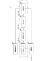
まず、本実施形態に係る光学モジュールおよび原子発振器について、図面を参照しながら説明する。本実施形態に係る原子発振器は、本実施形態に係る光学モジュールを含む。図1は、本実施形態に係る原子発振器1の機能ブロック図である。 First, an optical module and an atomic oscillator according to this embodiment will be described with reference to the drawings. The atomic oscillator according to the present embodiment includes the optical module according to the present embodiment. FIG. 1 is a functional block diagram of an atomic oscillator 1 according to this embodiment.
原子発振器1は、光学モジュール2と、制御手段50と、を含む。
The atomic oscillator 1 includes an
光学モジュール2は、光源10と、波長選択手段20と、ガスセル30と、光検出手段40と、を含む。
The
光源10は、中心波長(中心周波数)を有する基本波Fと、互いに異なる波長を有する第1側帯波W1および第2側帯波W2と、を含む第1光L1を発生させる。
The
波長選択手段20は、第1光L1の第1側帯波W1および第2側帯波W2を選択して透過することによって第2光L2を射出する。
The
ガスセル30は、アルカリ金属ガスを封入しており、ガスセル30には、第2光L2が照射される。
The
光検出手段40は、ガスセル30を透過した第2光L2の強度を検出する。
The light detection means 40 detects the intensity of the second light L2 that has passed through the
制御手段50は、光検出手段40の検出結果に基づいて、第1側帯波W1および第2側帯波W2の波長(周波数)差が、ガスセル30に封入されたアルカリ金属原子の2つの基底準位のエネルギー差に相当する周波数に等しくなるように制御する。具体的には、制御手段50は、光検出手段40の検出結果に基づいて、変調周波数fmを有する検出信号を発生させる。そして、光源10は、この変調信号に基づいて所定の周波数f0を有する基本波Fを変調して、周波数f1=f0+fmを有する第1側帯波W1、および周波数f2=f0−fmを有する第2側帯波W2を発生させる。
Based on the detection result of the light detection means 40, the control means 50 determines that the difference in wavelength (frequency) between the first sideband wave W1 and the second sideband wave W2 is two ground levels of alkali metal atoms enclosed in the
図2(A)は、アルカリ金属原子のΛ型3準位モデルと第1側帯波W1及び第2側帯波W2の関係を示す図である。図2(B)は、光源10において発生する第1光L1の周波数スペクトラムを示す図である。
FIG. 2A is a diagram showing the relationship between the Λ-type three-level model of alkali metal atoms and the first sideband wave W1 and the second sideband wave W2. FIG. 2B is a diagram illustrating a frequency spectrum of the first light L <b> 1 generated in the
図2(B)に示すように、光源10において発生する第1光L1は、中心周波数f0(=v/λ0:vは光の速度、λ0はレーザー光の中心波長)を有する基本波Fと、中心周波数f0に対して上側サイドバンドに周波数f1を有する第1側帯波W1と、中心周波数f0に対して下側サイドバンドに周波数f2を有する第2側帯波W2と、を含む。第1側帯波W1の周波数f1は、f1=f0+fmであり、第2側帯波W2の周波数f2は、f2=f0−fmである。
As shown in FIG. 2B, the first light L1 generated in the
図2(A)及び図2(B)に示すように、第1側帯波W1の周波数f1と第2側帯波W2の周波数f2との周波数差が、アルカリ金属原子の基底準位1と基底準位2のエネルギー差ΔE12に相当する周波数と一致している。したがって、アルカリ金属原子は、周波数f1を有する第1側帯波W1と周波数f2を有する第2側帯波W2によってEIT現象を起こす。
As shown in FIG. 2 (A) and FIG. 2 (B), the frequency difference between the frequency f 2 of the frequency f 1 and the second sideband wave W2 of the first sideband W1 is the ground level 1 of an alkali metal atom This corresponds to the frequency corresponding to the energy difference ΔE 12 of the
ここで、EIT現象について説明する。アルカリ金属原子と光との相互作用は、Λ型3準位系モデルで説明できることが知られている。図2(A)に示すように、アルカリ金属原子は2つの基底準位を有し、基底準位1と励起準位とのエネルギー差に相当する波長(周波数f1)を有する第1側帯波W1、あるいは基底準位2と励起準位とのエネルギー差に相当する波長(周波数f2)を有する第2側帯波W2を、それぞれ単独でアルカリ金属原子に照射すると、光吸収が起きる。ところが、図2(B)に示すように、このアルカリ金属原子に、周波数差f1−f2が基底準位1と基底準位2のエネルギー差ΔE12に相当する周波数と正確に一致する第1側帯波W1と第2側帯波W2を同時に照射すると、2つの基底準位の重ね合わせ状態、即ち量子干渉状態になり、励起準位への励起が停止して第1側帯波W1と第2側帯波W2がアルカリ金属原子を透過する透明化現象(EIT現象)が起きる。このEIT現象を利用し、第1側帯波W1と第2側帯波W2との周波数差f1−f2が基底準位1と基底準位2のエネルギー差ΔE12に相当する周波数からずれた時の光吸収挙動の急峻な変化を検出し制御することで、高精度な発振器をつくることができる。
Here, the EIT phenomenon will be described. It is known that the interaction between alkali metal atoms and light can be explained by a Λ-type three-level model. As shown in FIG. 2A, the alkali metal atom has two ground levels, and a first sideband having a wavelength (frequency f 1 ) corresponding to the energy difference between the ground level 1 and the excited level. When an alkali metal atom is irradiated with W1 or a second sideband wave W2 having a wavelength (frequency f 2 ) corresponding to the energy difference between the
図3は、波長選択手段20から射出された第2光L2の周波数スペクトラムを示す図である。
FIG. 3 is a diagram illustrating a frequency spectrum of the second light L2 emitted from the
第2光L2は、第1光L1と比べて、基本波Fが消滅または基本波Fの強度が減少した光である。図3の例では、第2光L2は、中心周波数f0に対して上側サイドバンドに周波数f1を有する第1側帯波W1、および中心周波数f0に対して下側サイドバンドに周波数f2を有する第2側帯波W2のみを有している。このように、光学モジュール2では、波長選択手段20によって、基本波Fの強度を減少または基本波Fを消滅させることができる。
The second light L2 is light in which the fundamental wave F disappears or the intensity of the fundamental wave F decreases compared to the first light L1. FIG The third example, the second light L2, the center frequency the first sideband having a frequency f 1 to the upper sideband with respect to f 0 W1, and the center frequency f 2 to the lower sideband with respect to the frequency f 0 Only the second sideband W2 having As described above, in the
以下、本実施形態の原子発振器のより具体的な構成について説明する。 Hereinafter, a more specific configuration of the atomic oscillator of this embodiment will be described.
図4は、原子発振器1の構成を示す図である。 FIG. 4 is a diagram showing the configuration of the atomic oscillator 1.
原子発振器1は、図4に示すように、光学モジュール2と、電流駆動回路150と、変調回路160と、を含む。
As shown in FIG. 4, the atomic oscillator 1 includes an
光学モジュール2は、半導体レーザー110と、波長選択素子120と、ガスセル130と、光検出器140と、を含む。
The
半導体レーザー110は、中心波長を有する基本波Fと、互いに異なる波長を有する第1側帯波W1および第2側帯波W2と、を含む第1光L1を発生させる。半導体レーザー110が出射するレーザー光(第1光L1)は、電流駆動回路150が出力する駆動電流によって中心周波数f0(中心波長λ0)が制御され、変調回路160の出力信号(変調信号)によって変調がかけられる。すなわち、電流駆動回路150による駆動電流に、変調信号の周波数成分を有する交流電流を重畳することにより、半導体レーザー110が出射する第1光L1に変調をかけることができる。これにより、第1光L1には、第1側帯波W1、および第2側帯波W2が生成される。半導体レーザー110において発生する光は、可干渉性を有するため、量子干渉効果を得るために好適である。
The
図2(B)に示すように、第1光L1は、中心周波数f0(=v/λ0:vは光の速度、λ0は第1光L1の中心波長)を有する基本波Fと、中心周波数f0に対して上側サイドバンドに周波数f1を有する第1側帯波W1と、中心周波数f0に対して下側サイドバンドに周波数f2を有する第2側帯波W2と、を含む。第1側帯波W1の周波数f1は、f1=f0+fmであり、第2側帯波W2の周波数f2は、f2=f0−fmである。 As shown in FIG. 2B, the first light L1 includes a fundamental wave F having a center frequency f 0 (= v / λ 0 : v is the speed of light, and λ 0 is the center wavelength of the first light L1). includes a first sideband W1 having a frequency f 1 to the upper sideband with respect to the center frequency f 0, and the second sideband wave W2 having a frequency f 2 to the lower sideband with respect to the center frequency f 0, the . Frequency f 1 of the first sideband W1 is f 1 = f 0 + f m , the frequency f 2 of the second sideband wave W2 is f 2 = f 0 -f m.
波長選択素子120は、第1光の第1側帯波W1および第2側帯波W2を選択して透過する。すなわち、波長選択素子120は、第1側帯波W1および第2側帯波W2に対する透過率が大きく、基本波Fに対する透過率が小さい。これにより、波長選択素子120に入射した第1光L1の基本波Fの強度を減少または基本波Fを消滅させて、第2光L2として射出することができる。すなわち、第2光L2は、第1光L1と比べて、基本波Fの強度が減少または基本波Fが消滅している。図3の例では、第2光L2は、中心周波数f0に対して上側サイドバンドに周波数f1を有する第1側帯波W1、および中心周波数f0に対して下側サイドバンドに周波数f2を有する第2側帯波W2のみを有している。
The
波長選択素子120は、後述するように、エタロンであってもよいし、ファイバーグレーティングであってもよい。
As will be described later, the
ガスセル130は、容器中に気体状のアルカリ金属原子(ナトリウム(Na)原子、ルビジウム(Rb)原子、セシウム(Cs)原子等)が封入されたものである。ガスセル130には、第2光L2が照射される。
The
このガスセル130に対して、アルカリ金属原子の2つの基底準位のエネルギー差に相当する周波数(波長)を有する2つの光波(第1側帯波および第2側帯波)が照射されると、アルカリ金属原子がEIT現象を起こす。例えば、アルカリ金属原子がセシウム原子であれば、D1線における基底準位1と基底準位2のエネルギー差に相当する周波数が9.19263・・・GHzなので、周波数差が9.19263・・・GHzの2つの光波が照射されるとEIT現象を起こす。
When this
光検出器140は、ガスセル130を透過した第2光L2を検出し、検出した光の量に応じた信号強度の信号を出力する。光検出器140の出力信号は電流駆動回路150および変調回路160に入力される。光検出器140は、フォトダイオードであってもよい。
The
電流駆動回路150は、光検出器140の出力信号に応じた大きさの駆動電流を発生して半導体レーザー110に供給し、第1光L1の中心周波数f0(中心波長λ0)を制御する。
The
半導体レーザー110、波長選択素子120、ガスセル130、光検出器140、電流駆動回路150を通るフィードバックループにより第1光の中心周波数f0(中心波長λ0)が微調整されて安定する。
The center frequency f 0 (center wavelength λ 0 ) of the first light is finely adjusted and stabilized by a feedback loop passing through the
変調回路160は、光検出器140の出力信号に応じた変調周波数fmを有する変調信号を発生させる。この変調信号は、光検出器140の出力信号が最大になるように変調周波数fmが微調整されながら半導体レーザー110に供給される。半導体レーザー110が出射するレーザー光は、変調信号により変調がかけられ、第1側帯波W1と第2側帯波W2を発生させる。
なお、半導体レーザー110、波長選択素子120、ガスセル130、光検出器140は、それぞれ図1の光源10、波長選択手段20、ガスセル30、光検出手段40に対応する。また、電流駆動回路150、変調回路160は、図1の制御手段50に対応する。
The
このような構成の原子発振器1において、半導体レーザー110が発生させる第1光L1の第1側帯波W1と第2側帯波W2の周波数差がガスセル130に含まれるアルカリ金属原子の2つの基底準位のエネルギー差に相当する周波数と正確に一致しなければ、アルカリ金属原子がEIT現象を起こさないため、第1側帯波W1と第2側帯波W2の周波数に応じて光検出器140の検出量は極めて敏感に変化する。そのため、半導体レーザー110、波長選択素子120、ガスセル130、光検出器140、および変調回路160を通るフィードバックループにより、第1側帯波W1と第2側帯波W2との周波数差がアルカリ金属原子の2つの基底準位のエネルギー差に相当する周波数と極めて正確に一致するようにフィードバック制御がかかる。その結果、変調周波数は極めて安定した周波数になるので、変調信号を原子発振器1の出力信号(クロック出力)とすることができる。
In the atomic oscillator 1 having such a configuration, the frequency difference between the first sideband wave W1 and the second sideband wave W2 of the first light L1 generated by the
図5は、光学モジュール2の要部(半導体レーザー110および波長選択素子120)を模式的に示す断面図である。
FIG. 5 is a cross-sectional view schematically showing main parts (
光学モジュール2は、図5に示すように、さらに、基体170を含む。半導体レーザー110および波長選択素子120は、基体170に形成されている。このように半導体レーザー110および波長選択素子120がモノリシックに形成されることにより、装置の小型化を図ることができる。
As shown in FIG. 5, the
基体170の材質は、化合物半導体である。具体的には、基体170の材質は、例えば、GaAs、InP、GaN等のIII-V族半導体や、ZnO、ZnSe等のII-VI族半導体である。ここでは、基体170の材質が第1導電型(例えばn型)GaAsである場合について説明する。
The material of the
半導体レーザー110は、第1半導体層112と、活性層114と、第2半導体層116と、を含む面発光型レーザーである。
The
第1半導体層112は、基体170上に形成されている。第1半導体層112は、例えば、n型(第1導電型)Al0.9Ga0.1As層とn型Al0.15Ga0.85As層とを交互に積層した分布ブラッグ反射型(DBR)半導体ミラーである。
The
活性層114は、第1半導体層112上に形成されている。活性層114は、例えば、GaAsウェル層とAl0.3Ga0.7Asバリア層とから構成される量子井戸構造を3つ重ねた多重量子井戸(MQW)構造を有する。
The
第2半導体層116は、例えば、p型(第2導電型)Al0.15Ga0.85As層とp型Al0.9Ga0.1As層とを交互に積層したDBR半導体ミラーである。
The
p型の第2半導体層116、不純物がドーピングされていない活性層114、およびn型の第1半導体層112により、pinダイオードが形成される。
The p-type
第1電極118は、基体170の下面に形成されている。第1電極118は、基体170を介して、第1半導体層112と電気的に接続されている。第1電極118は、半導体レーザー110を駆動するための一方の電極である。
The
第2電極119は、第2半導体層116の上面に形成されている。第2電極119は、第2半導体層116と電気的に接続されている。第2電極119は、半導体レーザー110を駆動するための他方の電極である。
The
第1電極118と第2電極119とで、pinダイオードに順方向の電圧を印加すると、活性層114において、電子と正孔との再結合が起こり、該再結合による発光が生じる。そこで生じた光が第2半導体層116と第1半導体層112との間を往復する際に誘導放出が起こり、光の強度が増幅される。光利得が光損失を上まわると、レーザー発振が起こり、第2半導体層116の上面からレーザー光(第1光L1)が出射される。半導体レーザー110から出射された光L1は、プリズム180で反射されて、波長選択素子120に入射する。プリズム180は、第1光L1の進行方向を変えて、第1光L1を波長選択素子120に入射させるための光学素子である。
When a forward voltage is applied to the pin diode between the
光学モジュール2において、波長選択素子120は、エタロンである。波長選択素子120は、第1ミラー121と、第2ミラー122と、第1ミラー121と第2ミラー122との間に配置された基板123と、を含む。
In the
波長選択素子120は、干渉作用により、入射した光のうち、所定波長の光(第1側帯波W1および第2側帯波W2)を透過する。第1ミラー121と第2ミラー122との間の基板123に光が入射すると、干渉作用により、基板123の長さ(第1ミラー121と第2ミラー122との間の距離)Dおよび基板123の屈折率に応じた波長の光が選択的に波長選択素子120を透過する。波長選択素子120は、第1側帯波W1および第2側帯波W2に対する透過率が大きく、基本波Fに対する透過率が小さい。これにより、波長選択素子120に入射した光L1の基本波Fの強度を減少または基本波Fを消滅させることができる。したがって、波長選択素子120は、例えば、第1側帯波W1および第2側帯波W2のみを含む第2光L2を射出することができる。
The
第1ミラー121と第2ミラー122は、基板123を介して、互いに対向している。第1ミラー121および第2ミラー122は、例えば、Ta2O5膜とSiO2膜とを交互に積層した多層膜からなる。
The
基板123は、基体170上に形成されている。基板123は、基体170側から順に形成された、第1層124、第2層126、および第3層128を有している。基板123は、第1層124の屈折率および第3層128の屈折率は、第2層126の屈折率より小さい。したがって、第1層124および第3層128は、クラッド層として機能し、第2層は、第1光L1を伝播させるコア層として機能する。すなわち、基板123は、第1光L1を伝搬させる光導波路である。光学モジュール2では、基板123が光導波路であるため、波長選択素子から射出される光L2のビーム径を制御することができ、ガスセル130に光を効率よく照射することができる。
The
第1層124および第3層128の材質は、例えば、AlGaAsであり、第2層126の材質は、例えば、GaAsである。
The material of the
基板123の材質は、特に限定されず、GaAs、InP、GaN等のIII-V族半導体や、ZnO、ZnSe等のII-VI族半導体であってもよい。基板123の材質として、例えば、GaAsを用いた場合、フリースペクトラルレンジを9.2GHz、半値全幅を0.3GHz程度とすると、基板123の長さDは28.5mm程度である。エタロンの基板の材質として一般的なSiO2を用いた場合、基板の長さは、70.66mm程度である。このように、基板123の材質として、屈折率の大きい化合物半導体を用いることで、基板123の長さDを短くすることができる。
The material of the
なお、基板123は、光導波路を形成しなくてもよい。基板123は、複数の層124,126,128を有さずに、単層であってもよい。
The
ここでは、波長選択素子120がエタロンである場合について説明したが、波長選択素子120は、光ファイバーのコアに長手方向に周期的な屈折率変化を与えたファイバーグレーティングであってもよい。ファイバーグレーティングは、光ファイバーを用いているため、変形が容易であり、設計の自由度を向上できる。
Here, the
光学モジュール2および原子発振器1は、例えば、以下の特徴を有する。
The
光学モジュール2によれば、波長選択素子120が、第1光L1の基本波Fの強度を減少または基本波Fを消滅させることができる。これにより、EIT現象に寄与しない基本波Fがアルカリ金属原子に照射されることを抑制または防止できる。したがって、ACシュタルク効果による周波数変動を抑制することができ、周波数安定度の高い発振器を提供できる。
According to the
光学モジュール2によれば、波長選択素子120が、エタロンである。したがって、簡易な構成で波長選択素子を形成できる。また、波長選択素子(エタロン)120の基板123の材質が化合物半導体である。したがって、基板123の材質をSiO2とした場合と比べて、基板123の長さDを短くすることができ、装置の小型化を図ることができる。
According to the
光学モジュール2によれば、波長選択素子(エタロン)120および半導体レーザー(光源)110が基体170に形成されている。このように波長選択素子120と半導体レーザー110を基体170にモノリシックに形成することにより、装置の小型化を図ることができる。
According to the
光学モジュール2によれば、上述のように、波長選択素子(エタロン)120の基板123が光導波路である。したがって、波長選択素子120から射出される光L2のビーム径を制御することができ、ガスセル130に効率よく光を照射することができる。
According to the
光学モジュール2によれば、光源10が面発光型レーザーである。面発光型レーザーは、端面発光型レーザーと比べて、ゲインを生じさせるための電流が少ないため、低消費電力化を図ることができる。
According to the
原子発振器1によれば、光学モジュール2を有している。したがって、上述のように、周波数安定度の高めることができる。
The atomic oscillator 1 has the
なお、上述した実施形態は一例であって、これらに限定されるわけではない。 The above-described embodiment is an example, and the present invention is not limited to these.
例えば、上述した図5に示す半導体レーザー110は、面発光型レーザーであったが、半導体レーザーは、端面発光型レーザーであってもよい。図6は、端面発光型レーザーを用いた光学モジュール2Dの要部を模式的に示す断面図である。以下、図6に示す光学モジュール2Dにおいて、上述した図5に示す光学モジュール2の構成と同様の構成については同一の符号を付し、その説明を省略する。
For example, although the
第1半導体層112は、基体170上に形成されている。第1半導体層112としては、例えば、第1導電型(例えばn型)AlGaAs層などを用いることができる。
The
活性層114は、第1半導体層112上に形成されている。活性層114は、例えば、GaAsウェル層とAlGaAsバリア層とから構成される量子井戸構造を3つ重ねた多重量子井戸(MQW)構造を有する。
The
第2半導体層116は、活性層114上に形成されている。第2半導体層116としては、例えば、第2導電型(例えばp型)のAlGaAs層などを用いることができる。
The
例えば、p型の第2半導体層116、不純物がドーピングされていない活性層114、およびn型の第1半導体層112により、pinダイオードが構成される。第2半導体層116および第1半導体層112の各々は、活性層114よりも禁制帯幅が大きく、屈折率が小さい層である。活性層114は、光を増幅する機能を有する。第1半導体層112および第2半導体層116は、活性層114を挟んで、注入キャリア(電子および正孔)並びに光を閉じ込める機能を有する。
For example, the p-type
半導体レーザー110では、第1電極118と第2電極119との間に、pinダイオードの順バイアス電圧を印加すると、活性層114において電子と正孔との再結合が起こる。この再結合により発光が生じる。この生じた光を起点として、連鎖的に誘導放出が起こり、光強度が増幅される。光利得が光損失を上まわると、レーザー発振が起こり、レーザー光が生じ、活性層114の側面からレーザー光(第1光L1)が出射される。
In the
半導体レーザー110として端面発光型レーザーを用いることで、半導体レーザー110の各層112,114,116の積層方向に対して垂直にレーザー光を出射することができる。したがって、各層112,114,116の膜厚の制御によって、半導体レーザー110と波長選択素子120との間のアライメントができる。さらに、例えば、同じ基体170上に形成された波長選択素子120にレーザー光を入射させるためのプリズム等の光学素子が不要となる。したがって、半導体レーザー110と波長選択素子120との間のアライメント精度を向上させることができる。
By using an edge-emitting laser as the
上記のように、本発明の実施形態について詳細に説明したが、本発明の新規事項および効果から実体的に逸脱しない多くの変形が可能であることは当業者には容易に理解できよう。従って、このような変形例はすべて本発明の範囲に含まれるものとする。 Although the embodiments of the present invention have been described in detail as described above, those skilled in the art will readily understand that many modifications are possible without substantially departing from the novel matters and effects of the present invention. Accordingly, all such modifications are intended to be included in the scope of the present invention.
1 原子発振器、2 光学モジュール、10 光源、20 波長選択手段、
30 ガスセル、40 光検出手段、50 制御手段、110 半導体レーザー、
112 第1半導体層、114 活性層、116 第2半導体層、118 第1電極、
119 第2電極、120 波長選択素子、121 第1ミラー、122 第2ミラー、
123 基板、124 第1層、126 第2層、128 第3層、130 ガスセル、
140 光検出器、150 電流駆動回路、160 変調回路、170 基体、
180 プリズム
1 atomic oscillator, 2 optical module, 10 light source, 20 wavelength selection means,
30 gas cell, 40 light detection means, 50 control means, 110 semiconductor laser,
112 first semiconductor layer, 114 active layer, 116 second semiconductor layer, 118 first electrode,
119 second electrode, 120 wavelength selection element, 121 first mirror, 122 second mirror,
123 substrate, 124 first layer, 126 second layer, 128 third layer, 130 gas cell,
140 photodetector, 150 current drive circuit, 160 modulation circuit, 170 substrate,
180 prism
Claims (9)
中心波長を有する基本波と、前記中心波長の第1側帯波および第2側帯波と、を含む第1光を発生させる光源と、
前記第1光の前記第1側帯波および前記第2側帯波を選択的に透過させることによって、第2光を射出する波長選択手段と、
アルカリ金属ガスを封入し、前記第2光が照射されるガスセルと、
前記ガスセルを透過した前記第2光の強度を検出する光検出手段と、
を含む、光学モジュール。 An optical module of an atomic oscillator using the quantum interference effect,
A light source that generates a first light including a fundamental wave having a center wavelength, and a first sideband and a second sideband of the center wavelength ;
By Rukoto selectively transmits the first sideband and the second sideband of the first light, and the wavelength selection means for emitting a second light,
A gas cell containing an alkali metal gas and irradiated with the second light;
Light detecting means for detecting the intensity of the second light transmitted through the gas cell;
Including an optical module.
前記波長選択手段は、エタロンである、光学モジュール。 In claim 1,
The optical module, wherein the wavelength selection means is an etalon.
前記エタロンは、
前記第1光を反射させ、互いに対向する第1ミラーおよび第2ミラーと、
前記第1ミラーと前記第2ミラーとの間に配置された基板と、
を有し、
前記基板の材質は、化合物半導体である、光学モジュール。 In claim 2,
The etalon is
A first mirror and a second mirror that reflect the first light and face each other;
A substrate disposed between the first mirror and the second mirror;
Have
An optical module in which the material of the substrate is a compound semiconductor.
さらに、基体を含み、
前記基体の材質は、化合物半導体であり、
前記光源は、半導体レーザーであり、
前記エタロンおよび前記光源は、基体に形成されている、光学モジュール。 In claim 3,
And further including a substrate,
The material of the substrate is a compound semiconductor,
The light source is a semiconductor laser;
The etalon and the light source are optical modules formed on a base.
前記エタロンの前記基板は、前記基体側から順に形成された第1層、第2層、および第3層を有し、
前記第1層の屈折率および前記第3層の屈折率は、前記第2層の屈折率より小さく、
前記第2層は、前記第1光を伝播させる、光学モジュール。 In claim 4,
The substrate of the etalon has a first layer, a second layer, and a third layer formed in order from the base side,
The refractive index of the first layer and the refractive index of the third layer are smaller than the refractive index of the second layer,
The second layer is an optical module for propagating the first light.
前記光源は、端面発光型レーザーである、光学モジュール。 In claim 4 or 5,
The optical module is an optical module, wherein the light source is an edge-emitting laser.
前記光源は、面発光型レーザーである、光学モジュール。 In any one of Claims 1 thru | or 5,
The optical module, wherein the light source is a surface emitting laser.
前記波長選択手段は、ファイバーグレーティングである、光学モジュール。 In claim 1,
The optical module, wherein the wavelength selection means is a fiber grating.
Priority Applications (11)
| Application Number | Priority Date | Filing Date | Title |
|---|---|---|---|
| JP2010159505A JP5699467B2 (en) | 2010-07-14 | 2010-07-14 | Optical module and atomic oscillator |
| KR1020110044952A KR101336453B1 (en) | 2010-07-14 | 2011-05-13 | Optical module and atomic oscillator |
| CN201610246819.5A CN105933002B (en) | 2010-07-14 | 2011-05-26 | Optical module and atomic oscillator |
| CN201110150422.3A CN102394646B (en) | 2010-07-14 | 2011-05-26 | Optical module and atomic oscillator |
| US13/162,916 US8476983B2 (en) | 2010-07-14 | 2011-06-17 | Optical module and atomic oscillator |
| TW104125478A TWI574511B (en) | 2010-07-14 | 2011-07-11 | Optical module and atomic oscillator |
| TW100124483A TWI501560B (en) | 2010-07-14 | 2011-07-11 | Optical module and atomic oscillator |
| EP11173564.3A EP2407834B1 (en) | 2010-07-14 | 2011-07-12 | Optical module and atomic oscillator |
| KR1020120105713A KR101658264B1 (en) | 2010-07-14 | 2012-09-24 | Optical module and atomic oscillator |
| US13/909,388 US9054638B2 (en) | 2010-07-14 | 2013-06-04 | Optical module and atomic oscillator |
| KR1020160115477A KR101690467B1 (en) | 2010-07-14 | 2016-09-08 | Optical module and atomic oscillator |
Applications Claiming Priority (1)
| Application Number | Priority Date | Filing Date | Title |
|---|---|---|---|
| JP2010159505A JP5699467B2 (en) | 2010-07-14 | 2010-07-14 | Optical module and atomic oscillator |
Related Child Applications (1)
| Application Number | Title | Priority Date | Filing Date |
|---|---|---|---|
| JP2013011894A Division JP5700056B2 (en) | 2013-01-25 | 2013-01-25 | Optical module and atomic oscillator |
Publications (3)
| Publication Number | Publication Date |
|---|---|
| JP2012023179A JP2012023179A (en) | 2012-02-02 |
| JP2012023179A5 JP2012023179A5 (en) | 2013-08-08 |
| JP5699467B2 true JP5699467B2 (en) | 2015-04-08 |
Family
ID=44800390
Family Applications (1)
| Application Number | Title | Priority Date | Filing Date |
|---|---|---|---|
| JP2010159505A Active JP5699467B2 (en) | 2010-07-14 | 2010-07-14 | Optical module and atomic oscillator |
Country Status (6)
| Country | Link |
|---|---|
| US (2) | US8476983B2 (en) |
| EP (1) | EP2407834B1 (en) |
| JP (1) | JP5699467B2 (en) |
| KR (3) | KR101336453B1 (en) |
| CN (2) | CN105933002B (en) |
| TW (2) | TWI501560B (en) |
Families Citing this family (23)
| Publication number | Priority date | Publication date | Assignee | Title |
|---|---|---|---|---|
| JP5699467B2 (en) | 2010-07-14 | 2015-04-08 | セイコーエプソン株式会社 | Optical module and atomic oscillator |
| JP5910808B2 (en) | 2011-03-14 | 2016-04-27 | セイコーエプソン株式会社 | Optical module and atomic oscillator for an atomic oscillator |
| JP6056118B2 (en) * | 2011-03-23 | 2017-01-11 | セイコーエプソン株式会社 | Optical module and atomic oscillator |
| JP2014053842A (en) * | 2012-09-10 | 2014-03-20 | Seiko Epson Corp | Method of manufacturing quantum interference device, quantum interference device, electronic apparatus, and atom cell module |
| US9116510B1 (en) * | 2012-12-06 | 2015-08-25 | The Boeing Company | Micro atomic and inertial measurement unit on a chip system |
| JP5700056B2 (en) * | 2013-01-25 | 2015-04-15 | セイコーエプソン株式会社 | Optical module and atomic oscillator |
| DE102013209751B3 (en) * | 2013-05-27 | 2014-04-03 | Siemens Aktiengesellschaft | Method for operating laser spectrometer for optical gas analysis in process measurement field, involves arranging structure on detector where structure incorporates etalons whose idle regions are chosen to be smaller than tuning region |
| JP2015079831A (en) * | 2013-10-16 | 2015-04-23 | セイコーエプソン株式会社 | Light-emitting device and atomic oscillator |
| JP6323650B2 (en) * | 2013-12-20 | 2018-05-16 | セイコーエプソン株式会社 | Surface emitting laser and atomic oscillator |
| JP6274404B2 (en) | 2013-12-20 | 2018-02-07 | セイコーエプソン株式会社 | Surface emitting laser and atomic oscillator |
| JP6410008B2 (en) * | 2013-12-20 | 2018-10-24 | セイコーエプソン株式会社 | Surface emitting laser and atomic oscillator |
| JP6299955B2 (en) * | 2013-12-20 | 2018-03-28 | セイコーエプソン株式会社 | Surface emitting laser and atomic oscillator |
| JP6323651B2 (en) | 2013-12-20 | 2018-05-16 | セイコーエプソン株式会社 | Surface emitting laser and atomic oscillator |
| JP6323649B2 (en) * | 2013-12-20 | 2018-05-16 | セイコーエプソン株式会社 | Surface emitting laser and atomic oscillator |
| CN103986062B (en) * | 2014-05-04 | 2017-09-12 | 中国科学院上海光学精密机械研究所 | Single beam saturated absorption frequency stabilization Optical devices |
| GB2532221B (en) * | 2014-11-11 | 2016-11-16 | Ibm | Equipment enclosure air flow control system |
| CN104767119B (en) * | 2015-03-24 | 2017-09-12 | 中国科学院上海光学精密机械研究所 | Regulable center frequency humorous frequency stabilizing device of semiconductor laser and frequency-stabilizing method |
| JP2017084936A (en) * | 2015-10-27 | 2017-05-18 | セイコーエプソン株式会社 | Light source and atomic oscillator |
| JP6757290B2 (en) * | 2017-05-09 | 2020-09-16 | 日本電信電話株式会社 | Light source device |
| FR3072512B1 (en) * | 2017-10-17 | 2021-06-11 | Thales Sa | IMPROVED RADIOFREQUENCY OSCILLATOR |
| US10364144B2 (en) * | 2017-11-17 | 2019-07-30 | Texas Instruments Incorporated | Hermetically sealed package for mm-wave molecular spectroscopy cell |
| KR102233366B1 (en) * | 2018-09-21 | 2021-03-30 | 한국표준과학연구원 | Resonator for atomic frequency standard and physics package including the resonator |
| CN114447752A (en) * | 2020-11-05 | 2022-05-06 | 中国科学院微电子研究所 | Wavelength selectable laser system |
Family Cites Families (43)
| Publication number | Priority date | Publication date | Assignee | Title |
|---|---|---|---|---|
| US3546622A (en) * | 1965-10-29 | 1970-12-08 | Lockheed Aircraft Corp | Laser having controlled frequency translation |
| US3363193A (en) * | 1966-02-18 | 1968-01-09 | Varian Associates | Adjustable frequency atomic frequency standard |
| US3720882A (en) * | 1970-08-03 | 1973-03-13 | Research Corp | Parametric frequency conversion |
| US4733397A (en) * | 1985-08-12 | 1988-03-22 | Electrical Power Research Institute, Inc. | Resonant cavity optical modulator |
| JPS6388883A (en) * | 1986-10-01 | 1988-04-19 | Nippon Telegr & Teleph Corp <Ntt> | Semiconductor integrated light source |
| JPH0353575A (en) * | 1989-07-21 | 1991-03-07 | Canon Inc | Wavelength stabilized semiconductor laser |
| US6222424B1 (en) * | 1999-11-18 | 2001-04-24 | Kernco, Inc. | Optically pumped atomic frequency standard |
| US6363091B1 (en) | 2000-06-05 | 2002-03-26 | Agilent Technologies, Inc | Coherent population trapping-based method for generating a frequency standard having a reduced magnitude of total a.c. stark shift |
| US6201821B1 (en) | 2000-06-05 | 2001-03-13 | Agilent Technologies, Inc. | Coherent population trapping-based frequency standard having a reduced magnitude of total a.c. stark shift |
| US6472943B1 (en) * | 2000-12-21 | 2002-10-29 | Telefonaktie Bolaget L.M. Ericsson | Oscillating circuit and method for calibrating same |
| US6806784B2 (en) | 2001-07-09 | 2004-10-19 | The National Institute Of Standards And Technology | Miniature frequency standard based on all-optical excitation and a micro-machined containment vessel |
| US6570459B1 (en) | 2001-10-29 | 2003-05-27 | Northrop Grumman Corporation | Physics package apparatus for an atomic clock |
| ATE445922T1 (en) * | 2002-04-09 | 2009-10-15 | California Inst Of Techn | ATOMIC CLOCK BASED ON AN OPTOELECTRONIC OSCILLATOR |
| US6900702B2 (en) | 2002-08-14 | 2005-05-31 | Honeywell International Inc. | MEMS frequency standard for devices such as atomic clock |
| US7098744B2 (en) * | 2002-12-18 | 2006-08-29 | Hrl Laboratories, Llc | Method and apparatus for generating two frequencies having a frequency separation equal to the atomic frequency of an atomic species |
| US6993058B2 (en) | 2003-04-28 | 2006-01-31 | Agilent Technologies, Inc. | Coherent population trapping detector |
| US20050073690A1 (en) | 2003-10-03 | 2005-04-07 | Abbink Russell E. | Optical spectroscopy incorporating a vertical cavity surface emitting laser (VCSEL) |
| US7378913B2 (en) * | 2003-11-26 | 2008-05-27 | Kernco, Inc. | Optically excited atomic frequency standard |
| JP4889951B2 (en) * | 2005-03-02 | 2012-03-07 | 住友大阪セメント株式会社 | Optical frequency stabilizer |
| US7791790B2 (en) | 2005-11-04 | 2010-09-07 | Panasonic Corporation | Wavelength converter |
| US8805136B2 (en) | 2006-05-08 | 2014-08-12 | Photonics On-Fiber Devices, Inc. | On-fiber tunable Bragg gratings for DWDM applications |
| JP4720635B2 (en) | 2006-06-14 | 2011-07-13 | エプソントヨコム株式会社 | Atomic oscillator, passive atomic oscillator, temperature control method for atomic oscillator, and temperature control method for passive atomic oscillator |
| US7457495B2 (en) | 2006-10-05 | 2008-11-25 | Harris Corporation | Method of filtering optical signals with a capillary waveguide tunable optical device |
| TWI341138B (en) * | 2006-10-16 | 2011-04-21 | Corning Inc | Wavelength control in wavelength selective, phase, and gain regions of semiconductor lasers |
| JP4608512B2 (en) * | 2007-03-30 | 2011-01-12 | 日本電信電話株式会社 | Frequency stabilized light source |
| US7773883B1 (en) * | 2007-05-04 | 2010-08-10 | Vello Systems, Inc. | Single-fiber optical ring networks based on optical double sideband modulation |
| JP2009049623A (en) | 2007-08-17 | 2009-03-05 | Epson Toyocom Corp | Atomic oscillator |
| JP2009089116A (en) | 2007-10-01 | 2009-04-23 | Epson Toyocom Corp | Optical module for atomic oscillator |
| JP2009129955A (en) | 2007-11-20 | 2009-06-11 | Epson Toyocom Corp | Optical system, and atomic oscillator |
| JP2009141048A (en) * | 2007-12-05 | 2009-06-25 | Epson Toyocom Corp | Optical system and atomic oscillator |
| JP2009164331A (en) | 2008-01-07 | 2009-07-23 | Epson Toyocom Corp | Atomic oscillator and oscillation device |
| JP2009182562A (en) | 2008-01-30 | 2009-08-13 | Epson Toyocom Corp | Optical system and atomic oscillator |
| JP4952603B2 (en) | 2008-02-05 | 2012-06-13 | セイコーエプソン株式会社 | Atomic oscillator |
| CN101990742A (en) * | 2008-02-07 | 2011-03-23 | L·甘 | Device, system, and method of frequency generation using an atomic resonator |
| JP5045478B2 (en) * | 2008-02-12 | 2012-10-10 | セイコーエプソン株式会社 | Atomic oscillator |
| JP2010147967A (en) | 2008-12-22 | 2010-07-01 | Epson Toyocom Corp | Atomic oscillator and method of stabilizing frequency thereof |
| US8237514B2 (en) * | 2009-02-06 | 2012-08-07 | Seiko Epson Corporation | Quantum interference device, atomic oscillator, and magnetic sensor |
| CN101656537B (en) * | 2009-07-21 | 2012-04-04 | 中国科学院武汉物理与数学研究所 | Method and device for preparing multi-pulse interference Ramsey-CPT stripe |
| JP5589166B2 (en) * | 2009-11-12 | 2014-09-17 | セイコーエプソン株式会社 | Atomic oscillator |
| JP5699467B2 (en) | 2010-07-14 | 2015-04-08 | セイコーエプソン株式会社 | Optical module and atomic oscillator |
| JP5910807B2 (en) | 2011-03-14 | 2016-04-27 | セイコーエプソン株式会社 | Optical module and atomic oscillator for an atomic oscillator |
| JP5910808B2 (en) * | 2011-03-14 | 2016-04-27 | セイコーエプソン株式会社 | Optical module and atomic oscillator for an atomic oscillator |
| JP6056118B2 (en) | 2011-03-23 | 2017-01-11 | セイコーエプソン株式会社 | Optical module and atomic oscillator |
-
2010
- 2010-07-14 JP JP2010159505A patent/JP5699467B2/en active Active
-
2011
- 2011-05-13 KR KR1020110044952A patent/KR101336453B1/en active IP Right Grant
- 2011-05-26 CN CN201610246819.5A patent/CN105933002B/en not_active Expired - Fee Related
- 2011-05-26 CN CN201110150422.3A patent/CN102394646B/en active Active
- 2011-06-17 US US13/162,916 patent/US8476983B2/en active Active
- 2011-07-11 TW TW100124483A patent/TWI501560B/en not_active IP Right Cessation
- 2011-07-11 TW TW104125478A patent/TWI574511B/en not_active IP Right Cessation
- 2011-07-12 EP EP11173564.3A patent/EP2407834B1/en not_active Not-in-force
-
2012
- 2012-09-24 KR KR1020120105713A patent/KR101658264B1/en active IP Right Grant
-
2013
- 2013-06-04 US US13/909,388 patent/US9054638B2/en active Active
-
2016
- 2016-09-08 KR KR1020160115477A patent/KR101690467B1/en active IP Right Grant
Also Published As
| Publication number | Publication date |
|---|---|
| KR20120007442A (en) | 2012-01-20 |
| US8476983B2 (en) | 2013-07-02 |
| CN105933002B (en) | 2018-11-27 |
| KR20160111350A (en) | 2016-09-26 |
| TW201543820A (en) | 2015-11-16 |
| JP2012023179A (en) | 2012-02-02 |
| CN102394646A (en) | 2012-03-28 |
| KR20120126035A (en) | 2012-11-20 |
| CN105933002A (en) | 2016-09-07 |
| CN102394646B (en) | 2016-05-18 |
| EP2407834A1 (en) | 2012-01-18 |
| KR101336453B1 (en) | 2013-12-04 |
| TWI574511B (en) | 2017-03-11 |
| EP2407834B1 (en) | 2014-08-13 |
| TW201203868A (en) | 2012-01-16 |
| US9054638B2 (en) | 2015-06-09 |
| KR101690467B1 (en) | 2016-12-27 |
| US20120013411A1 (en) | 2012-01-19 |
| TWI501560B (en) | 2015-09-21 |
| KR101658264B1 (en) | 2016-09-20 |
| US20130265113A1 (en) | 2013-10-10 |
Similar Documents
| Publication | Publication Date | Title |
|---|---|---|
| JP5699467B2 (en) | Optical module and atomic oscillator | |
| JP5910806B2 (en) | Optical module and atomic oscillator for an atomic oscillator | |
| JP6102525B2 (en) | Surface emitting laser element and atomic oscillator | |
| JP5910807B2 (en) | Optical module and atomic oscillator for an atomic oscillator | |
| JP2012191121A (en) | Optical module for atomic oscillator, and atomic oscillator | |
| JP6056118B2 (en) | Optical module and atomic oscillator | |
| JP5700056B2 (en) | Optical module and atomic oscillator | |
| JP2019062036A (en) | Modulation light source | |
| JP2015128172A (en) | Optical module and atomic oscillator | |
| JP2008130666A (en) | Semiconductor light-emitting device | |
| JP6705151B2 (en) | Atomic oscillator | |
| JP2010102045A (en) | Mode synchronization semiconductor laser | |
| JP2014022667A (en) | Vertical cavity surface emitting laser element, and atomic oscillator | |
| JP2016072371A (en) | Atom oscillator | |
| JP2013229357A (en) | Distribution feedback type semiconductor laser and otdr device | |
| JP2017084935A (en) | Atomic oscillator |
Legal Events
| Date | Code | Title | Description |
|---|---|---|---|
| A521 | Request for written amendment filed |
Free format text: JAPANESE INTERMEDIATE CODE: A523 Effective date: 20130624 |
|
| A621 | Written request for application examination |
Free format text: JAPANESE INTERMEDIATE CODE: A621 Effective date: 20130624 |
|
| A977 | Report on retrieval |
Free format text: JAPANESE INTERMEDIATE CODE: A971007 Effective date: 20140217 |
|
| A131 | Notification of reasons for refusal |
Free format text: JAPANESE INTERMEDIATE CODE: A131 Effective date: 20140304 |
|
| A521 | Request for written amendment filed |
Free format text: JAPANESE INTERMEDIATE CODE: A523 Effective date: 20140411 |
|
| A131 | Notification of reasons for refusal |
Free format text: JAPANESE INTERMEDIATE CODE: A131 Effective date: 20140701 |
|
| A521 | Request for written amendment filed |
Free format text: JAPANESE INTERMEDIATE CODE: A523 Effective date: 20140827 |
|
| RD04 | Notification of resignation of power of attorney |
Free format text: JAPANESE INTERMEDIATE CODE: A7424 Effective date: 20150106 |
|
| TRDD | Decision of grant or rejection written | ||
| A01 | Written decision to grant a patent or to grant a registration (utility model) |
Free format text: JAPANESE INTERMEDIATE CODE: A01 Effective date: 20150120 |
|
| A61 | First payment of annual fees (during grant procedure) |
Free format text: JAPANESE INTERMEDIATE CODE: A61 Effective date: 20150202 |
|
| R150 | Certificate of patent or registration of utility model |
Ref document number: 5699467 Country of ref document: JP Free format text: JAPANESE INTERMEDIATE CODE: R150 |
|
| S531 | Written request for registration of change of domicile |
Free format text: JAPANESE INTERMEDIATE CODE: R313531 |
|
| R350 | Written notification of registration of transfer |
Free format text: JAPANESE INTERMEDIATE CODE: R350 |
|
| S111 | Request for change of ownership or part of ownership |
Free format text: JAPANESE INTERMEDIATE CODE: R313113 |
|
| R350 | Written notification of registration of transfer |
Free format text: JAPANESE INTERMEDIATE CODE: R350 |
|
| R250 | Receipt of annual fees |
Free format text: JAPANESE INTERMEDIATE CODE: R250 |
|
| R250 | Receipt of annual fees |
Free format text: JAPANESE INTERMEDIATE CODE: R250 |