JP5609130B2 - Atomic oscillator - Google Patents
Atomic oscillator Download PDFInfo
- Publication number
- JP5609130B2 JP5609130B2 JP2010020946A JP2010020946A JP5609130B2 JP 5609130 B2 JP5609130 B2 JP 5609130B2 JP 2010020946 A JP2010020946 A JP 2010020946A JP 2010020946 A JP2010020946 A JP 2010020946A JP 5609130 B2 JP5609130 B2 JP 5609130B2
- Authority
- JP
- Japan
- Prior art keywords
- frequency
- light
- signal
- atomic oscillator
- lights
- Prior art date
- Legal status (The legal status is an assumption and is not a legal conclusion. Google has not performed a legal analysis and makes no representation as to the accuracy of the status listed.)
- Expired - Fee Related
Links
Images


Classifications
-
- H—ELECTRICITY
- H01—ELECTRIC ELEMENTS
- H01S—DEVICES USING THE PROCESS OF LIGHT AMPLIFICATION BY STIMULATED EMISSION OF RADIATION [LASER] TO AMPLIFY OR GENERATE LIGHT; DEVICES USING STIMULATED EMISSION OF ELECTROMAGNETIC RADIATION IN WAVE RANGES OTHER THAN OPTICAL
- H01S1/00—Masers, i.e. devices using stimulated emission of electromagnetic radiation in the microwave range
- H01S1/06—Gaseous, i.e. beam masers
-
- G—PHYSICS
- G04—HOROLOGY
- G04F—TIME-INTERVAL MEASURING
- G04F5/00—Apparatus for producing preselected time intervals for use as timing standards
- G04F5/14—Apparatus for producing preselected time intervals for use as timing standards using atomic clocks
- G04F5/145—Apparatus for producing preselected time intervals for use as timing standards using atomic clocks using Coherent Population Trapping
-
- H—ELECTRICITY
- H03—ELECTRONIC CIRCUITRY
- H03B—GENERATION OF OSCILLATIONS, DIRECTLY OR BY FREQUENCY-CHANGING, BY CIRCUITS EMPLOYING ACTIVE ELEMENTS WHICH OPERATE IN A NON-SWITCHING MANNER; GENERATION OF NOISE BY SUCH CIRCUITS
- H03B17/00—Generation of oscillations using radiation source and detector, e.g. with interposed variable obturator
-
- H—ELECTRICITY
- H03—ELECTRONIC CIRCUITRY
- H03L—AUTOMATIC CONTROL, STARTING, SYNCHRONISATION, OR STABILISATION OF GENERATORS OF ELECTRONIC OSCILLATIONS OR PULSES
- H03L7/00—Automatic control of frequency or phase; Synchronisation
- H03L7/26—Automatic control of frequency or phase; Synchronisation using energy levels of molecules, atoms, or subatomic particles as a frequency reference
Landscapes
- Physics & Mathematics (AREA)
- Electromagnetism (AREA)
- Engineering & Computer Science (AREA)
- Plasma & Fusion (AREA)
- Optics & Photonics (AREA)
- Spectroscopy & Molecular Physics (AREA)
- Life Sciences & Earth Sciences (AREA)
- Ecology (AREA)
- General Physics & Mathematics (AREA)
- Stabilization Of Oscillater, Synchronisation, Frequency Synthesizers (AREA)
- Semiconductor Lasers (AREA)
Description
本発明は、原子発振器に関する。 The present invention relates to an atomic oscillator.
電磁誘起透過(EIT:Electromagnetically Induced Transparency)方式(CPT(Coherent Population Trapping)方式と呼ばれることもある)による原子発振器は、アルカリ金属原子に、可干渉性(コヒーレント性)を有し、かつ、互いに異なる特定の波長(周波数)を有する2種類の共鳴光を同時に照射すると共鳴光の吸収が停止する現象を利用した発振器である。 An atomic oscillator based on an electromagnetically induced transparency (EIT) system (sometimes called a CPT (Coherent Population Trapping) system) has coherency with alkali metal atoms and is different from each other. This is an oscillator using a phenomenon in which absorption of resonance light stops when two types of resonance light having a specific wavelength (frequency) are simultaneously irradiated.
アルカリ金属原子と2種類の共鳴光との相互作用機構は、図17(A)に示すように、Λ型3準位系モデルで説明できることが知られている。アルカリ金属原子は2つの基底準位を有し、基底準位1と励起準位とのエネルギー差に相当する周波数を有する共鳴光1、あるいは基底準位2と励起準位とのエネルギー差に相当する周波数を有する共鳴光2を、それぞれ単独でアルカリ金属原子に照射すると、よく知られているように光吸収が起きる。ところが、このアルカリ金属原子に共鳴光1と共鳴光2を同時に照射すると、2つの基底準位の重ね合わせ状態、即ち量子干渉状態になり、励起準位への励起が停止して共鳴光1と共鳴光2がアルカリ金属原子を透過する透明化現象(EIT現象)が起きる。従って、アルカリ金属原子に周波数の異なる2種類の光を照射したとき、この2種類の光が共鳴光対となってアルカリ金属原子がEIT現象を起こすか否かで光吸収挙動が急峻に変化する。この共鳴光対の周波数差は2つの基底準位のエネルギー差ΔE12に相当する周波数(例えば、セシウム原子であれば9.192631770GHz)と正確に一致する。そこで、光吸収挙動の急峻な変化を検出し、アルカリ金属原子に照射する2種類の光が共鳴光対となるように、すなわち、この2種類の光の周波数差がΔE12に相当する周波数と正確に一致するように周波数制御することで、高精度な発振器を実現することができる。
It is known that the interaction mechanism between an alkali metal atom and two types of resonance light can be explained by a Λ-type three-level model as shown in FIG. The alkali metal atom has two ground levels, and corresponds to the
図18は、従来のEIT方式による原子発振器の一般的な構成の概略図である。図18に示すように、従来のEIT方式による原子発振器は、電流駆動回路により発生した周波数f0(=v/λ0:vは光の速度、λ0は光の波長)を設定するための駆動電流に、周波数がfmの変調信号を重畳することにより、半導体レーザーに変調をかけて周波数がf0+fmの光と周波数がf0−fmの光を発生させる。この2種類の光はガスセルに同時に照射され、光検出器によりガスセルを透過した光の強度を検出する。ガスセルは気体状のアルカリ金属原子とこれを封入する容器とから構成されており、同時に照射された2種類の光が共鳴光対となれば、アルカリ金属原子がEIT現象を起こし、ガスセルを透過する光の強度が大きくなる。そこで、この原子発振器は、低周波発振器が発生する数十Hz〜数百Hz程度の低周波信号を用いて検波を行うことで、検出強度が最大付近になるように電圧制御水晶発振器(VCXO:Voltage Controlled Crystal Oscillator)の発振周波数を制御し、PLL(Phase Locked Loop)を介して変調信号を生成する。このような構成によれば、図17(B)に示すように、半導体レーザーが出射する周波数がf0+fmの光と周波数がf0−fmの光が共鳴光対となるように、すなわち、変調信号の周波数fmがΔE12に相当する周波数の1/2の周波数と一致するように制御がかかる。従って、電圧制御水晶発振器(VCXO)の発振動作が極めて安定に継続し、周波数安定度が極めて高い発振信号を発生させることができる。 FIG. 18 is a schematic diagram of a general configuration of a conventional atomic oscillator based on the EIT method. As shown in FIG. 18, the conventional atomic oscillator according to the EIT method is used to set the frequency f 0 (= v / λ 0 : v is the speed of light and λ 0 is the wavelength of light) generated by the current driving circuit. the drive current by the frequency superimposing a modulated signal f m, frequency by modulating the semiconductor laser light and a frequency of f 0 + f m generates the light of f 0 -f m. These two types of light are simultaneously irradiated onto the gas cell, and the intensity of the light transmitted through the gas cell is detected by a photodetector. The gas cell is composed of a gaseous alkali metal atom and a container that encloses the gas. If two types of light irradiated at the same time form a resonant light pair, the alkali metal atom causes an EIT phenomenon and passes through the gas cell. The intensity of light increases. Therefore, this atomic oscillator performs detection using a low-frequency signal of about several tens Hz to several hundreds Hz generated by a low-frequency oscillator, so that a voltage control crystal oscillator (VCXO: The oscillation frequency of a voltage controlled crystal oscillator is controlled, and a modulation signal is generated via a PLL (Phase Locked Loop). According to this structure, as shown in FIG. 17 (B), such that the frequency of the semiconductor laser emits the light and the frequency of f 0 + f m becomes light resonant light pair of f 0 -f m, that is, the frequency f m of the modulation signal is applied is controlled so as to coincide with half the frequency of the frequency corresponding to the Delta] E 12. Therefore, the oscillation operation of the voltage controlled crystal oscillator (VCXO) can be continued extremely stably, and an oscillation signal with extremely high frequency stability can be generated.
しかしながら、従来の原子発振器では、ΔE12に相当する周波数の1/2の周波数と正確に一致する周波数fmの変調信号を発生させるために、電圧制御水晶発振器(VCXO)、検波回路、変調回路、低周波発振器、PLL等が必要となるため、回路の複雑化が避けられず、小型化や省電力化が難しいという問題があった。 However, in the conventional atomic oscillator, to generate a modulated signal of a frequency f m that exactly matches the one half of the frequency of the frequency corresponding to Delta] E 12, a voltage controlled crystal oscillator (VCXO), a detection circuit, a modulation circuit In addition, since a low frequency oscillator, a PLL, and the like are required, there is a problem in that the circuit is complicated and it is difficult to reduce the size and power consumption.
本発明は、以上のような問題点に鑑みてなされたものであり、本発明のいくつかの態様によれば、回路部分の小型化や省電力化が容易な原子発振器を提供することができる。 The present invention has been made in view of the above problems, and according to some aspects of the present invention, it is possible to provide an atomic oscillator in which the circuit portion can be easily reduced in size and power consumption. .
(1)本発明は、金属原子と、
周波数が異なる電磁誘起透過現象を起こす一対の光を含む複数の光を前記金属原子に照射する光源と、
前記金属原子を通過した前記複数の光の干渉からビート信号を生成する光検出部と、
前記ビート信号に基づいて、前記一対の光の少なくとも一つの光の周波数を制御する周波数制御部と、
を含み、
前記周波数制御部は、前記光検出部で生成されたビート信号から所定の周波数の前記ビート信号を選択して通過させるフィルターと、前記フィルターを通過したビート信号を増幅する信号増幅部と、を有し、前記信号増幅部が増幅した信号に基づいて前記一対の光の少なくとも一つの光の周波数を制御することを特徴とする。
(1) The present invention comprises a metal atom,
A light source that irradiates the metal atoms with a plurality of lights including a pair of lights that cause electromagnetically induced transmission phenomena having different frequencies; and
A light detection unit that generates a beat signal from the interference of the plurality of lights that have passed through the metal atoms;
A frequency controller that controls the frequency of at least one of the pair of lights based on the beat signal;
Including
The frequency control unit includes a filter that selectively passes the beat signal having a predetermined frequency from the beat signal generated by the light detection unit, and a signal amplification unit that amplifies the beat signal that has passed through the filter. The frequency of at least one of the pair of lights is controlled based on the signal amplified by the signal amplifying unit.
EIT方式による従来の原子発振器では、光検出器の出力信号がDC(直流)もしくは数十〜数百Hz程度の低周波数であったため電圧制御水晶発振器(VCXO)やPLLを用いてGHz帯の高周波信号を生成して光源に対する周波数制御を行う必要があった。これに対し、本発明に係る原子発振器では、アルカリ金属原子を透過した複数の光の干渉により得られる所定の周波数のビート信号を含む検出信号、すなわち、高周波(GHz帯)の検出信号を生成する。そして、周波数制御部は、この高周波の検出信号に基づいて、第1の光と第2の光が共鳴光対となるように周波数制御を行うのでPLLが不要である。 In the conventional atomic oscillator using the EIT system, the output signal of the photodetector is DC (direct current) or a low frequency of about several tens to several hundreds Hz, so that a high frequency in the GHz band using a voltage controlled crystal oscillator (VCXO) or PLL is used. It was necessary to generate a signal and perform frequency control on the light source. On the other hand, the atomic oscillator according to the present invention generates a detection signal including a beat signal of a predetermined frequency obtained by interference of a plurality of lights that have passed through alkali metal atoms, that is, a detection signal of a high frequency (GHz band). . Since the frequency control unit performs frequency control so that the first light and the second light form a resonant light pair based on the high-frequency detection signal, no PLL is required.
さらに、本発明の原子発振器では、第1の光と第2の光の周波数差がアルカリ金属原子の2つの基底準位のエネルギー差に相当する周波数と一致する前後で、アルカリ金属原子を透過する光の強度が急激に変化する。すなわち、アルカリ金属原子の透過特性に基づく極めて狭い帯域制限フィルターが形成される。従って、第1の光と第2の光の周波数差が、アルカリ金属原子の2つの基底準位のエネルギー差に相当する周波数と一致する状態から少しずれると、この帯域制限フィルターの効果によって、アルカリ金属原子の2つの基底準位のエネルギー差に相当する周波数と一致するようにフィードバック制御がかかる。そのため、本発明の原子発振器では、検波回路や電圧制御水晶発振器(VCXO)が無くても第1の光と第2の光の周波数差の微妙な調整が行われ、安定した発振動作を継続することができる。 Furthermore, in the atomic oscillator of the present invention, the alkali metal atom is transmitted before and after the frequency difference between the first light and the second light matches the frequency corresponding to the energy difference between the two ground levels of the alkali metal atom. The intensity of light changes rapidly. That is, a very narrow band limiting filter based on the transmission characteristics of alkali metal atoms is formed. Therefore, when the frequency difference between the first light and the second light is slightly deviated from the state corresponding to the frequency corresponding to the energy difference between the two ground levels of the alkali metal atom, the effect of the band limiting filter causes the alkali difference. Feedback control is applied so as to coincide with the frequency corresponding to the energy difference between the two ground levels of the metal atom. Therefore, in the atomic oscillator of the present invention, even if there is no detection circuit or voltage controlled crystal oscillator (VCXO), fine adjustment of the frequency difference between the first light and the second light is performed, and stable oscillation operation is continued. be able to.
従って、本発明によれば、従来の原子発振器と比較して回路部分の小型化や省電力化が容易な原子発振器を提供することができる。 Therefore, according to the present invention, it is possible to provide an atomic oscillator in which a circuit portion can be easily reduced in size and power can be saved as compared with a conventional atomic oscillator.
本発明の原子発振器によれば、周波数制御に必要な所定の周波数のビート信号がフィルターによって選択されるので、その他の不要なビート信号の影響で安定した発振動作が妨げられることを防止することができる。 According to the atomic oscillator of the present invention, since a beat signal having a predetermined frequency necessary for frequency control is selected by a filter, it is possible to prevent a stable oscillation operation from being hindered by the influence of other unnecessary beat signals. it can.
このようにすれば、検出信号のレベルが十分でない場合であっても、周波数制御の安定性を確保することができる。 In this way, it is possible to ensure the stability of frequency control even when the level of the detection signal is not sufficient.
(2)この原子発振器は、前記金属原子を通過した前記複数の光のうち、光学フィルターを通過した一対の光が前記ビート信号を生じるようにしてもよい。 ( 2 ) In this atomic oscillator, a pair of lights that have passed through an optical filter among the plurality of lights that have passed through the metal atoms may generate the beat signal .
このようにしても、不要なビート信号の影響で安定した発振動作が妨げられることを防止することができる。 Even in this case, it is possible to prevent the stable oscillation operation from being hindered by the influence of an unnecessary beat signal.
(3)この原子発振器において、前記周波数制御部は、前記ビート信号の周波数を変換する周波数変換部を有し、前記周波数変換部が変換した周波数の信号に基づいて前記一対の光の少なくとも一つの光の周波数を制御するようにしてもよい。 ( 3 ) In this atomic oscillator, the frequency control unit has a frequency conversion unit that converts the frequency of the beat signal, and at least one of the pair of lights based on the frequency signal converted by the frequency conversion unit The frequency of light may be controlled .
(4)この原子発振器において、前記ビート信号の周波数は、前記一対の光の周波数差の1/2であってもよい。 ( 4 ) In this atomic oscillator, the frequency of the beat signal may be ½ of the frequency difference between the pair of lights .
(5)この原子発振器において、前記ビート信号の周波数が、前記一対の光の周波数差と等しくてもよい。 ( 5 ) In this atomic oscillator, the frequency of the beat signal may be equal to the frequency difference between the pair of lights .
以下、本発明の好適な実施形態について図面を用いて詳細に説明する。なお、以下に説明する実施の形態は、特許請求の範囲に記載された本発明の内容を不当に限定するものではない。また以下で説明される構成の全てが本発明の必須構成要件であるとは限らない。 DESCRIPTION OF EMBODIMENTS Hereinafter, preferred embodiments of the present invention will be described in detail with reference to the drawings. The embodiments described below do not unduly limit the contents of the present invention described in the claims. Also, not all of the configurations described below are essential constituent requirements of the present invention.
図1は、本実施形態の原子発振器の機能ブロック図である。 FIG. 1 is a functional block diagram of the atomic oscillator of this embodiment.
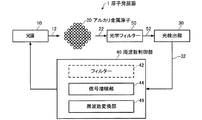
本実施形態の原子発振器1は、光源10、アルカリ金属原子20、光検出部30及び周波数制御部40を含んで構成されている。
The
光源10は、可干渉性(コヒーレント性)を有し、周波数が異なる第1の光と第2の光を含む複数の光12を発生させて気体状のアルカリ金属原子20(ナトリウム(Na)原子、ルビジウム(Rb)原子、セシウム(Cs)原子等)に照射する。例えば、レーザー光は可干渉性(コヒーレント性)を有する光である。
The
光検出部30は、アルカリ金属原子20を透過した複数の光(透過光)22を受け取り、当該複数の光22の干渉により得られる所定の周波数のビート信号を含む検出信号32を生成する。所定の周波数とは、例えば、第1の光と第2の光の周波数差と等しい周波数であったり、第1の光と第2の光の周波数差の1/2の周波数であってもよい。
The
ここで、例えば、気体状のアルカリ金属原子20を密閉容器に封入したガスセルを光源10と光検出部30の間に配置するような形態でもよい。また、密閉容器内に光源10、気体状のアルカリ金属20、光検出部30を共に封入し、光源10と光検出部30を対向させて配置するような形態でもよい。
Here, for example, a configuration in which a gas cell in which gaseous alkali metal atoms 20 are sealed in a sealed container is disposed between the
周波数制御部40は、検出信号32に含まれる所定の周波数のビート信号に基づいて、第1の光と第2の光がアルカリ金属原子20にEIT現象を起こさせる共鳴光対となるように、第1の光及び第2の光の少なくとも一方の周波数制御を行う。ここで、共鳴光対とは、可干渉性を有し、アルカリ金属原子20にEIT現象を起こさせる周波数の異なる2種類の光であり、その周波数差がアルカリ金属原子20の2つの基底準位のエネルギー差に相当する周波数と正確に一致する場合だけでなく、アルカリ金属原子20がEIT現象を起こす範囲の微小な誤差を含んでいてもよい。
Based on the beat signal of a predetermined frequency included in the
また、周波数制御部40は、フィルター42、信号増幅部44、周波数変換部46の少なくとも1つを含むように構成されていてもよい。フィルター42は、検出信号32から所定の周波数のビート信号を選択して通過させる。信号増幅部44は、検出信号32又はフィルター42が選択したビート信号を増幅する。周波数変換部46は、光検出部30の検出信号32に含まれる所定の周波数のビート信号を異なる周波数の信号に変換する。そして、周波数制御部40は、フィルター42が選択したビート信号や信号増幅部44が増幅した信号や周波数変換部46が変換した信号に基づいて、第1の光及び第2の光の少なくとも一方の周波数制御を行うようにしてもよい。
The frequency control unit 40 may be configured to include at least one of a
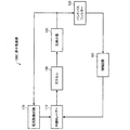
さらに、図2に示すように、本実施形態の原子発振器1は、光学フィルター50を含んで構成されていてもよい。光学フィルター50は、アルカリ金属原子20を透過した複数の光22から所定の周波数のビート信号を生じさせる2つの光52を選択して通過させる。なお、原子発振器1は、フィルター42の代わりに光学フィルター50を含むようにしてもよいし、光学フィルター50とフィルター42の両方を含むようにしてもよい。
Further, as shown in FIG. 2, the
以下、本実施形態の原子発振器のより具体的な構成について説明する。 Hereinafter, a more specific configuration of the atomic oscillator of this embodiment will be described.
(1)第1実施形態
図3は、第1実施形態の原子発振器の構成を示す図である。
(1) First Embodiment FIG. 3 is a diagram illustrating a configuration of an atomic oscillator according to a first embodiment.
図3に示すように、第1実施形態の原子発振器100Aは、半導体レーザー110、ガスセル120、光検出器130、バンドパスフィルター140、増幅回路150、周波数変換回路160、電流駆動回路170を含んで構成されている。
As shown in FIG. 3, the atomic oscillator 100A of the first embodiment includes a
ガスセル120は、容器中に気体状のアルカリ金属原子が封入されたものであり、このガスセル120に対して、可干渉性を有し、アルカリ金属原子の2つの基底準位のエネルギー差ΔE12に相当する周波数f12と一致する周波数差を有する2種類の光(例えばレーザー光)を同時に照射すると、アルカリ金属原子がEIT現象を起こす。
The
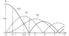
図4は、周波数がそれぞれf1とf2の2種類のレーザー光を、f2を固定してf1を変化させながらガスセル120に同時に照射したときの透過特性を示す概略図である。図4において、横軸は2種類のレーザー光の周波数差f1−f2であり、縦軸は透過光の強度である。
FIG. 4 is a schematic diagram showing transmission characteristics when two types of laser beams having frequencies f 1 and f 2 are simultaneously irradiated to the
図4に示すように、2種類のレーザー光の周波数差f1−f2がf12±δの範囲にあれば(f12はΔE12に相当する周波数)、この2種類のレーザー光が共鳴光対となってアルカリ金属原子がEIT現象を起こす。従って、f1−f2がf12±δの範囲では透過光の強度が急激に上昇する。そして、f1−f2がf12と一致するとき、EIT現象により光吸収を停止するアルカリ金属原子の数が最大になるため、透過光の強度が極大となる。例えば、セシウム原子は、D2線(波長は852.1nm)の基底状態が超微細構造によってF=3、4の準位を有する2つの状態に分裂しており、F=3の基底準位1とF=4の基底準位2のエネルギー差に相当する周波数は9.192631770GHzである。従って、セシウム原子に、波長が852.1nm付近で周波数差が9.192631770GHzの2種類のレーザー光が同時に照射されると、これら2種類のレーザー光が共鳴光対となってEIT現象が起こり、透過光の強度が極大となる。
As shown in FIG. 4, if the frequency difference f 1 -f 2 between the two types of laser beams is in the range of f 12 ± δ (f 12 is a frequency corresponding to ΔE 12 ), the two types of laser beams will resonate. Alkali metal atoms cause an EIT phenomenon as a light pair. Therefore, the intensity of transmitted light increases rapidly when f 1 −f 2 is in the range of f 12 ± δ. When f 1 -f 2 coincides with f 12 , the number of alkali metal atoms that stop light absorption due to the EIT phenomenon is maximized, so that the intensity of transmitted light is maximized. For example, in the cesium atom, the ground state of the D2 line (wavelength is 852.1 nm) is split into two states having F = 3 and 4 levels by the hyperfine structure, and the
半導体レーザー110は、周波数の異なる複数の光を発生させてガスセル120に照射する。具体的には、電流駆動回路170が出力する駆動電流によって、半導体レーザー110の出射光の中心波長λ0(中心波長はf0)がアルカリ金属原子の所定の輝線(例えば、セシウム原子のD2線)の波長と一致するように制御される。また、半導体レーザー110は、周波数変換回路160の出力信号(周波数fm)を変調信号として変調がかけられる。すなわち、電流駆動回路170による駆動電流に、周波数変換回路160の出力信号(変調信号)を重畳することにより、半導体レーザー110は変調がかかった光を発生させる。このような半導体レーザー110は、例えば、端面発光レーザー(Edge Emitting Laser)や、垂直共振器面発光レーザー(VCSEL:Vertical Cavity Surface Emitting Laser)等の面発光レーザーなどで実現することができる。
The
図5は、本実施形態における半導体レーザーの出射光の周波数スペクトルを示す概略図である。図5において、横軸は光の周波数であり、縦軸は光の強度である。 FIG. 5 is a schematic diagram showing the frequency spectrum of the emitted light of the semiconductor laser in the present embodiment. In FIG. 5, the horizontal axis represents the light frequency, and the vertical axis represents the light intensity.
図5に示すように、半導体レーザー110は、周波数f0の光Cと、その両側に周波数がf0±n×fm(nは正の整数)の複数の光を発生させる。そして、本実施形態では、1次のサイドバンドである光A(周波数はf0−fm)と光B(周波数はf0+fm)の周波数差がΔE12に相当する周波数と一致するように(言い換えれば、周波数fmがΔE12に相当する周波数の1/2と一致するように)制御がかかる(この制御がかかる原理については後述する)。例えば、アルカリ金属原子がセシウム原子であれば、光Aと光Bの周波数差(2×fm)が9.192631770GHzとなるように(周波数fmが4.596315885GHzとなるように)制御がかかる。
5, the
半導体レーザー110の出射光はガスセル120に照射され、ガスセル120を透過した複数の光(透過光)は互いに重なりあってうなり(光ビート)を生じさせる。このうなりの周期に応じて、透過光の全体としての強度(明暗)が周期的に変化する。
The light emitted from the
光検出器130は、この透過光の強度の周期的な変化を検出することで、うなりの周波数(ビート周波数)と等しい周波数のビート信号を含む検出信号を出力する。具体的には、周波数の異なる複数の透過光の間でうなりが生じるので、光検出器130の出力信号(検出信号)には、N×fm(Nは正の整数)のビート周波数を有する複数のビート信号が含まれる。例えば、図5に示した光A、B、Cにそれぞれ対応する3つの透過光をそれぞれA’、B’、C’とすると、透過光A’と透過光B’によるビート周波数は2×fm(=ΔE12に相当する周波数f12)であり、透過光A’と透過光C’又は透過光B’と透過光C’によるビート周波数はfm(=ΔE12に相当する周波数f12の1/2)である。このような光検出器130としては、例えば、光通信の分野で用いられている、GHzオーダーの周期で光の明滅を検出可能なフォトデテクターを利用することができる。
The
電流駆動回路170は、光検出器130の出力信号(検出信号)の強度が極大になるように駆動電流を調整することで、磁場変化や温度変化等の外乱の影響をキャンセルして、半導体レーザー110の出射光の中心周波数f0(中心波長λ0)を安定させることができる。
The
バンドパスフィルター140は、光検出器130の出力信号(検出信号)から、周波数が2×fm(=f12)のビート信号を選択して出力する。例えば、アルカリ金属原子がセシウム原子であれば、バンドパスフィルター140は、9.1926GHz程度の周波数のビート信号を選択して出力する。このようなバンドパスフィルター140は、2×fmのビート周波数が通過帯域に含まれ、その他のビート周波数が通過帯域に含まれないようなバンドパスフィルターとして実現することができる。
The
増幅回路150は、バンドパスフィルター140の出力信号の振幅を所定の増幅率で増幅する。光検出器130の検出感度や半導体レーザー110の変調感度に応じて、増幅回路150の増幅率を適切な値に設定することにより、フィードバック制御の安定性を確保することができる。
The
周波数変換回路160は、増幅回路150の出力信号の周波数をその1/2の周波数に変換する。例えば、アルカリ金属原子がセシウム原子であれば、増幅回路150の出力信号の周波数は9.192GHz程度であるので、周波数変換回路160により4.596GHz程度の周波数の信号に変換される。周波数変換回路160は、簡単な分周回路で実現することができる。
The
そして、半導体レーザー110は、周波数変換回路160の出力信号を変調信号として変調がかけられ、図5に示した光A、B、Cを発生させる。
The
なお、半導体レーザー110、光検出器130は、それぞれ図1の光源10、光検出部30に対応する。また、バンドパスフィルター140、増幅回路150、周波数変換回路160、電流駆動回路170で構成される回路は、図1の周波数制御部40に対応する。また、バンドパスフィルター140、増幅回路150、周波数変換回路160は、それぞれ図1のフィルター42、信号増幅部44、周波数変換部46に対応する。
The
このような構成の原子発振器100Aにおいて、光Aと光Bの周波数差2×fmがf12と一致するように(言い換えれば、周波数fmが周波数f12の1/2と一致するように)制御がかかる原理について、図6(A)、図6(B)、図6(C)を用いて説明する。なお、光Aの周波数をf2、光Bの周波数をf1とする。
In the atomic oscillator 100A of this configuration, as the
図6(A)、図6(B)、図6(C)において、Tは図4のf12±δ付近を拡大した透過特性を表し、S1、S2、S3は出射光の周波数スペクトルを示している。図6(A)、図6(B)、図6(C)において、横軸は、光Bと光Aの周波数差f1−f2であり、縦軸は出射光又は透過光の強度である。 6 (A), 6 (B), and 6 (C), T represents transmission characteristics in the vicinity of f 12 ± δ in FIG. 4, and S1, S2, and S3 represent frequency spectra of the emitted light. ing. 6A, 6B, and 6C, the horizontal axis represents the frequency difference f 1 -f 2 between the light B and the light A, and the vertical axis represents the intensity of the emitted light or transmitted light. is there.
まず、光Bと光Aの周波数差f1−f2(=2×fm)の平均値がf12と一致するとき(fmの平均値=f12×1/2のとき)は、図6(A)に示すように、ガスセル120において、光Aと光Bに対して斜線部分は吸収され、斜線部分以外は透過する。従って、透過光B’と透過光A’の平均周波数差もf12と一致し、透過光A’と透過光B’によるビート信号の周波数の平均値はf12である。このとき、変調信号の周波数fmの平均値はf12/2のまま変わらないので、この条件で周波数制御のフィードバックループが安定する。
First, the average value of the frequency difference of the light B and the light A f 1 -f 2 (= 2 × f m) is (when the average value = f 12 × 1/2 of f m) when matching the f 12 is As shown in FIG. 6A, in the
図6(A)の状態で、例えば磁場変化や温度変化等の外乱の影響で、透過光B’と透過光A’の平均周波数差がf12−Δfに変動したとする。このとき、透過光A’と透過光B’によるビート信号の周波数の平均値もf12−Δfに変動するので、変調信号の周波数fmの平均値が(f12−Δf)/2に変動する。すると、光Bと光Aの周波数差f1−f2(=2×fm)の平均値がf12−Δfに変動し、図6(B)に示すように、ガスセル120において、光Aと光Bに対して斜線部分は吸収され、斜線部分以外は透過するため、透過光B’と透過光A’の平均周波数差はf12−Δfよりも高くなる。従って、透過光A’と透過光B’によるビート信号の周波数の平均値が上昇し、変調信号の周波数fmの平均値も上昇する。そのため、光Bと光Aの周波数差f1−f2(=2×fm)の平均値も上昇する。この周波数制御のフィードバックループにより、図6(A)の状態、すなわち出射光Bと出射光Aの平均周波数差がf12と一致する状態(fmの平均値=f12×1/2)に引き戻す作用が働く。
In the state of FIG. 6A, it is assumed that the average frequency difference between the transmitted light B ′ and the transmitted light A ′ fluctuates to f 12 −Δf due to the influence of disturbance such as a magnetic field change and a temperature change. At this time, since the fluctuation mean value to f 12 -.DELTA.f frequency of the transmitted light A 'and the transmitted light B' beat signal by the mean value (f 12 -.DELTA.f) of the frequency f m of the modulation signal / 2 to change To do. Then, the average value of the frequency difference f 1 −f 2 (= 2 × f m ) between the light B and the light A changes to f 12 −Δf, and as shown in FIG. And the light B are absorbed in the shaded portion and the other portions are transmitted, so that the average frequency difference between the transmitted light B ′ and the transmitted light A ′ is higher than f 12 −Δf. Accordingly, the average value of the frequency of the transmitted light A 'and the transmitted light B' beat signal due rises, also rises the average value of the frequency f m of the modulation signal. Therefore, the average value of the
逆に、図6(A)の状態で、例えば磁場変化や温度変化等の外乱の影響で、透過光B’と透過光A’の平均周波数差がf12+Δfに変動したとする。このとき、透過光A’と透過光B’によるビート信号の周波数の平均値もf12+Δfに変動するので、変調信号の周波数fmの平均値が(f12+Δf)/2に変動する。すると、光Bと光Aの周波数差f1−f2(=2×fm)の平均値がf12+Δfに変動し、図6(C)に示すように、ガスセル120において、光Aと光Bに対して斜線部分は吸収され、斜線部分以外は透過するため、透過光B’と透過光A’の平均周波数差はf12+Δfよりも低くなる。従って、透過光A’と透過光B’によるビート信号の周波数の平均値が下降し、変調信号の周波数fmの平均値も下降する。そのため、光Bと光Aの周波数差f1−f2(=2×fm)の平均値も下降する。この周波数制御のフィードバックループにより、図6(A)の状態、すなわち光Bと光Aの平均周波数差がf12と一致する状態(fmの平均値=f12/2)に引き戻す作用が働く。
Conversely, in the state of FIG. 6A, it is assumed that the average frequency difference between the transmitted light B ′ and the transmitted light A ′ fluctuates to f 12 + Δf due to the influence of disturbance such as magnetic field change and temperature change. At this time, since the change in the average value also f 12 + Delta] f of the frequency of the transmitted light A 'and the transmitted light B' beat signal by the mean value of the frequency f m of the modulation signal is varied to (f 12 + Δf) / 2 . Then, the average value of the frequency difference f 1 −f 2 (= 2 × f m ) between the light B and the light A changes to f 12 + Δf, and as shown in FIG. Since the shaded portion is absorbed with respect to the light B and the portions other than the shaded portion are transmitted, the average frequency difference between the transmitted light B ′ and the transmitted light A ′ is lower than f 12 + Δf. Accordingly, the average value of the frequency of the transmitted light A 'and the transmitted light B' beat signal due is lowered, also lowered the average value of the frequency f m of the modulation signal. Therefore, also lowered the average value of the
なお、光検出器の出力信号(検出信号)には透過光A’と透過光B’によるビート信号(周波数が2×fmのビート信号)以外のビート信号も含まれる。そこで、本実施形態では、周波数が2×fmのビート信号による安定したフィードバック制御がかかるように、バンドパスフィルター140によって帯域制限がかけられている。
Incidentally, the beat signal by the output signal (detection signal) 'the transmitted light B as' the transmitted light A photodetector (frequency beat
以上に説明したように、第1実施形態の原子発振器では、ガスセル120の透過特性を利用することで、光Bと光Aの周波数差がΔE12に相当する周波数と一致するように、すなわち、光Aと光Bが共鳴光対となるようにフィードバック制御がかかる。このフィードバック制御は、図3に示したような、従来の構成と比較して極めて簡単な構成の回路で実現することができる。従って、第1実施形態によれば、回路部分の小型化や省電力化が容易な原子発振器を実現することができる。
As described above, in the atomic oscillator of a first embodiment, by utilizing the transmission characteristics of the
[変形例]
図7は、第1実施形態の原子発振器の変形例の構成を示す図である。図7に示すように、変形例の原子発振器100Bは、図3に示した原子発振器100Aに対して、電気光学変調器(EOM:Electro-Optic Modulator)180が追加されている。
[Modification]
FIG. 7 is a diagram illustrating a configuration of a modification of the atomic oscillator according to the first embodiment. As shown in FIG. 7, an atomic oscillator 100 </ b> B according to the modified example includes an electro-optic modulator (EOM) 180 added to the atomic oscillator 100 </ b> A shown in FIG. 3.
図7に示すように、原子発振器100Bでは、半導体レーザー110は、周波数変換回路160の出力信号(変調信号)による変調をかけずに、単一周波数f0の光を発生させる。この周波数f0の光は、電気光学変調器(EOM)180に入射し、周波数変換回路160の出力信号(変調信号)によって変調がかけられる。その結果、図5と同様の周波数スペクトルを有する光を発生させることができる。
As shown in FIG. 7, in the atomic oscillator 100B, the
図7に示す原子発振器100Bにおけるその他の構成は、図3に示した原子発振器100Aと同じであるため同じ番号を付しており、その説明を省略する。 The other configurations of the atomic oscillator 100B shown in FIG. 7 are the same as those of the atomic oscillator 100A shown in FIG.
なお、電気光学変調器(EOM)180の代わりに、音響光学変調器(AOM:Acousto-Optic Modulator)を用いてもよい。 Note that an acousto-optic modulator (AOM) may be used instead of the electro-optic modulator (EOM) 180.
なお、半導体レーザー110と電気光学変調器(EOM)180による構成が図1の光源10に対応する。その他の対応関係は、図3に示した原子発振器100Aと同じである。
The configuration of the
また、原子発振器100Aのその他の変形例として、バンドパスフィルター140の代わりに、ガスセル120と光検出器130の間に所望の特性を有する光学フィルターを設けた構成の原子発振器にすることもできる。
As another modification of the atomic oscillator 100A, an atomic oscillator having a configuration in which an optical filter having desired characteristics is provided between the
この光学フィルターは、例えば、図8において破線で示すような周波数特性を有し、透過光A’と透過光B’を選択的に通過させる。このようにすれば、透過光A’と透過光B’により発生する周波数が2×fmのうなり以外は無視できるほど小さくなり、不要なビート信号の影響で安定した発振動作が妨げられることを防止することができる。なお、この光学フィルターは図2の光学フィルター50に対応する。
For example, the optical filter has frequency characteristics as indicated by a broken line in FIG. 8 and selectively transmits the transmitted light A ′ and the transmitted light B ′. In this way, except the transmitted light A 'and the transmitted light B' is a frequency generated by 2 × f m Nounari be more reduced ignored, that the stable oscillation operation by the influence of the unwanted beat signals interfere Can be prevented. This optical filter corresponds to the
これらの変形例のような構成によっても、原子発振器100Aと同様の機能及び効果を有する原子発振器を実現することができる。 Even with configurations such as these modifications, an atomic oscillator having the same functions and effects as the atomic oscillator 100A can be realized.
(2)第2実施形態
図9は、第2実施形態の原子発振器の構成を示す図である。図9に示すように、第2実施形態の原子発振器100Cは、図3に示した第1実施形態の原子発振器100Aに対して、周波数変換回路160が無く、バンドパスフィルター140がバンドパスフィルター190に置き換わっている。
(2) Second Embodiment FIG. 9 is a diagram illustrating a configuration of an atomic oscillator according to a second embodiment. As shown in FIG. 9, the atomic oscillator 100 </ b> C of the second embodiment is different from the atomic oscillator 100 </ b> A of the first embodiment shown in FIG. 3 in that there is no
本実施形態では、半導体レーザー110は、電流駆動回路170が出力する駆動電流によって中心周波数f0(中心波長λ0)が制御され、増幅回路150の出力信号(周波数がfmの変調信号)によって変調がかけられる。すなわち、電流駆動回路170による駆動電流に、増幅回路150の出力信号(変調信号)による交流電流を重畳することにより、半導体レーザー110に変調がかかる。
In the present embodiment, the
そして、半導体レーザー110は、中心波長λ0がアルカリ金属原子の所定の輝線(例えば、セシウム原子のD2線)の波長と一致するとともに、増幅回路150の出力信号(変調信号)の周波数fmがΔE12に相当する周波数f12の1/2の周波数と一致するように制御がかかる。例えば、アルカリ金属原子がセシウム原子であれば、中心波長λ0はD2線の波長(852.1nm)と一致し、周波数fmは4.596315885GHz(=9.192631770GHz×1/2)と一致する。従って、本実施形態においても、半導体レーザー110の出射光の周波数スペクトルは図5と同様であり、光Aと光Bが共鳴光対となる。
Then, the
バンドパスフィルター190は、光検出器130の出力信号(検出信号)から、光Aと光B(共鳴光対)の周波数差の1/2の周波数のビート信号、すなわち、周波数がfmのビート信号を選択して出力する。例えば、アルカリ金属原子がセシウム原子であれば、バンドパスフィルター190は、4.596315885GHzのビート信号を選択して出力する。
Band-
このようなバンドパスフィルター190は、fmのビート周波数が通過帯域に含まれ、その他のビート周波数が通過帯域に含まれないようなバンドパスフィルターとして実現することができる。
Such band-
増幅回路150は、バンドパスフィルター190の出力信号の振幅を増幅して出力する。そして、半導体レーザー110は、増幅回路150の出力信号を変調信号として変調がかけられ、図5に示した光A、B、Cを発生させる。
The
原子発振器100Cにおけるその他の構成は、図3に示した原子発振器100Aと同じであるため同じ番号を付しており、その説明を省略する。 The other configurations in the atomic oscillator 100C are the same as those in the atomic oscillator 100A shown in FIG.
なお、半導体レーザー110、光検出器130は、それぞれ図1の光源10、光検出部30に対応する。また、バンドパスフィルター190、増幅回路150、電流駆動回路170で構成される回路は、図1の周波数制御部40に対応する。また、バンドパスフィルター190、増幅回路150は、それぞれ図1のフィルター42、信号増幅部44に対応する。
The
このような構成の原子発振器100Cでも、原子発振器100Aと同様の原理により、光Bと光Aの周波数差2×fmがΔE12に相当する周波数と一致するように、すなわち、光Aと光Bが共鳴光対となるようにフィードバック制御がかかる。このフィードバック制御は、図9に示したような、従来の構成と比較して極めて簡単な構成の回路で実現することができる。従って、第2実施形態によれば、回路部分の小型化や省電力化が容易な原子発振器を実現することができる。
Even atomic oscillator 100C having such a configuration, the same principle as the atomic oscillator 100A, so that the
[変形例]
原子発振器100Cにおいても、半導体レーザー110の駆動電流に変調信号を重畳する代わりに、図7に示した原子発振器100Bのように、電気光学変調器(EOM)や音響光学変調器(AOM)を用いて半導体レーザー110の出射光に変調をかけるように構成してもよい。
[Modification]
Also in the atomic oscillator 100C, instead of superimposing the modulation signal on the driving current of the
また、原子発振器100Cのその他の変形例として、バンドパスフィルター190の代わりに、ガスセル120と光検出器130の間に所望の特性を有する光学フィルターを設けた構成の原子発振器にすることもできる。
As another modification of the atomic oscillator 100C, an atomic oscillator having a configuration in which an optical filter having desired characteristics is provided between the
この光学フィルターは、例えば、図10において破線又は一点鎖線のいずれかで示すような周波数特性を有し、透過光A’と透過光C’又は透過光B’と透過光C’を選択的に通過させる。このようにすれば、透過光A’と透過光C’又は透過光B’と透過光C’により発生する周波数がfmのうなり以外は無視できるほど小さくなり、不要なビート信号の影響で安定した発振動作が妨げられることを防止することができる。なお、この光学フィルターは図2の光学フィルター50に対応する。
This optical filter has, for example, frequency characteristics as indicated by either a broken line or a one-dot chain line in FIG. 10, and selectively transmits light A ′ and transmitted light C ′ or transmitted light B ′ and transmitted light C ′. Let it pass. Thus, the frequency generated by 'and the transmitted light C' the transmitted light A 'transmitted light C and' or transmitted light B is negligibly small except f m Nounari, stability under the influence of unwanted beat signal This prevents the oscillating operation from being hindered. This optical filter corresponds to the
これらの変形例のような構成によっても、原子発振器100Cと同様の機能及び効果を有する原子発振器を実現することができる。 Even with configurations such as these modifications, an atomic oscillator having functions and effects similar to those of the atomic oscillator 100C can be realized.
(3)第3実施形態
図11は、第3実施形態の原子発振器の構成を示す図である。図11に示すように、第3実施形態の原子発振器100Dは、図3に示した第1実施形態の原子発振器100Aに対して、周波数変換回路160が無く、バンドパスフィルター140がバンドパスフィルター200に置き換わっている。
(3) Third Embodiment FIG. 11 is a diagram illustrating a configuration of an atomic oscillator according to a third embodiment. As shown in FIG. 11, the atomic oscillator 100 </ b> D of the third embodiment is different from the atomic oscillator 100 </ b> A of the first embodiment shown in FIG. 3 in that there is no
本実施形態では、半導体レーザー110は、電流駆動回路170が出力する駆動電流によって中心周波数f0(中心波長λ0)が制御され、増幅回路150の出力信号(周波数がfmの変調信号)によって変調がかけられる。すなわち、電流駆動回路170による駆動電流に、増幅回路150の出力信号(変調信号)による交流電流を重畳することにより、半導体レーザー110に変調がかかる。
In the present embodiment, the
そして、半導体レーザー110は、中心波長λ0がアルカリ金属原子の所定の輝線(例えば、セシウム原子のD2線)の波長と一致するとともに、増幅回路150の出力信号(変調信号)の周波数fmがΔE12に相当する周波数と一致するように制御がかかる。例えば、アルカリ金属原子がセシウム原子であれば、中心波長λ0はD2線の波長(852.1nm)と一致し、周波数fmは9.192631770GHzと一致する。
Then, the
図12は、本実施形態における半導体レーザーの出射光の周波数スペクトルを示す概略図である。図12において、横軸は光の周波数であり、縦軸は光の強度である。 FIG. 12 is a schematic diagram showing the frequency spectrum of the emitted light of the semiconductor laser in the present embodiment. In FIG. 12, the horizontal axis represents the light frequency, and the vertical axis represents the light intensity.
図12に示すように、半導体レーザー110は、周波数f0の光Cと、その両側に周波数がf0±n×fm(nは正の整数)の複数の光を発生させる。そして、1次のサイドバンドである光A、光Bと光Cの周波数差がいずれもΔE12に相当する周波数と一致するように(言い換えれば、周波数fmがΔE12に相当する周波数と一致するように)制御がかかる。
As shown in FIG. 12, the
例えば、アルカリ金属原子がセシウム原子であれば、光Aと光Cの周波数差及び光Bと光Cの周波数差(いずれもfm)が9.192631770GHzとなるように制御がかかる。 For example, if the alkali metal atom is a cesium atom, the frequency difference between the light A and the light C and the frequency difference between the light B and the light C (both f m ) are controlled to be 9.1926331770 GHz.
このように、本実施形態では、光Aと光C、光Bと光Cがそれぞれ共鳴光対となってEIT現象を起こすので、その周波数差がΔE12に相当する周波数と一致する付近で、光A、光B、光Cの透過率が急激に変動する。 Thus, in the present embodiment, the light A and light C, since the light B and the light C is a respective resonant light pair causes EIT phenomenon, around which matches the frequency of the frequency difference is equivalent to Delta] E 12, The transmittance of light A, light B, and light C changes rapidly.
そして、周波数の異なる複数の透過光の間でうなりが生じるので、光検出器130の出力信号(検出信号)には、N×fm(Nは正の整数)のビート周波数を有する複数の信号が含まれる。例えば、図12に示した光A、B、Cにそれぞれ対応する3つの透過光をそれぞれA’、B’、C’とすると、透過光A’と透過光B’によるビート周波数は2×fm(=ΔE12に相当する周波数の2倍)であり、透過光A’と透過光C’又は透過光B’と透過光C’によるビート周波数はfm(=ΔE12に相当する周波数)である。
Since beats occur between a plurality of transmitted lights having different frequencies, the output signal (detection signal) of the
バンドパスフィルター200は、光検出器130の出力信号(検出信号)から、光Aと光C又は光Bと光C(いずれも共鳴光対)の周波数差と等しい周波数のビート信号、すなわち、周波数がfmのビート信号を選択して出力する。例えば、アルカリ金属原子がセシウム原子であれば、バンドパスフィルター190は、9.192631770GHzのビート信号を選択して出力する。
The band-
このようなバンドパスフィルター200は、fmのビート周波数が通過帯域に含まれ、その他のビート周波数が通過帯域に含まれないようなバンドパスフィルターとして実現することができる。
Such band-
増幅回路150は、バンドパスフィルター200の出力信号の振幅を増幅して出力する。そして、半導体レーザー110は、増幅回路150の出力信号を変調信号として変調がかけられ、図12に示した光A、B、Cを発生させる。
The
原子発振器100Dにおけるその他の構成は、図3に示した原子発振器100Aと同じであるため同じ番号を付しており、その説明を省略する。 The other configuration of the atomic oscillator 100D is the same as that of the atomic oscillator 100A shown in FIG.
なお、半導体レーザー110、光検出器130は、それぞれ図1の光源10、光検出部30に対応する。また、バンドパスフィルター200、増幅回路150、電流駆動回路170で構成される回路は、図1の周波数制御部40に対応する。また、バンドパスフィルター200、増幅回路150は、それぞれ図1のフィルター42、信号増幅部44に対応する。
The
このような構成の原子発振器100Dでも、原子発振器100Aと同様の原理により、光Aと光Cの周波数差及び光Bと光Cの周波数差がいずれもΔE12に相当する周波数と一致するように、すなわち、光Aと光C、光Bと光Cがそれぞれ共鳴光対となるようにフィードバック制御がかかる。このフィードバック制御は、図11に示したような、従来の構成と比較して極めて簡単な構成の回路で実現することができる。従って、第3実施形態によれば、回路部分の小型化や省電力化が容易な原子発振器を実現することができる。 Also in the atomic oscillator 100D having such a configuration, the frequency difference between the light A and the light C and the frequency difference between the light B and the light C are all matched with the frequency corresponding to ΔE 12 by the same principle as the atomic oscillator 100A. That is, feedback control is applied so that the light A and the light C, and the light B and the light C form a resonant light pair. This feedback control can be realized by a circuit having a very simple configuration as compared with the conventional configuration as shown in FIG. Therefore, according to the third embodiment, an atomic oscillator in which the circuit portion can be easily reduced in size and power can be realized.
[変形例]
原子発振器100Dにおいても、半導体レーザー110の駆動電流に変調信号を重畳する代わりに、図7に示した原子発振器100Bのように、電気光学変調器(EOM)や音響光学変調器(AOM)を用いて半導体レーザー110の出射光に変調をかけるように構成してもよい。
[Modification]
Also in the atomic oscillator 100D, instead of superimposing the modulation signal on the driving current of the
また、原子発振器100Dのその他の変形例として、バンドパスフィルター200の代わりに、ガスセル120と光検出器130の間に所望の特性を有する光学フィルターを設けた構成の原子発振器にすることもできる。
As another modification of the atomic oscillator 100D, an atomic oscillator having a configuration in which an optical filter having desired characteristics is provided between the
この光学フィルターは、例えば、図13において破線又は一点鎖線のいずれかで示すような周波数特性を有し、透過光A’と透過光C’又は透過光B’と透過光C’を選択的に通過させる。このようにすれば、透過光A’と透過光C’又は透過光B’と透過光C’により発生する周波数がfmのうなり以外は無視できるほど小さくなり、不要なビート信号の影響で安定した発振動作が妨げられることを防止することができる。なお、この光学フィルターは図2の光学フィルター50に対応する。
For example, this optical filter has frequency characteristics as indicated by either a broken line or a one-dot chain line in FIG. 13, and selectively transmits light A ′ and transmitted light C ′ or transmitted light B ′ and transmitted light C ′. Let it pass. Thus, the frequency generated by 'and the transmitted light C' the transmitted light A 'transmitted light C and' or transmitted light B is negligibly small except f m Nounari, stability under the influence of unwanted beat signal This prevents the oscillating operation from being hindered. This optical filter corresponds to the
これらの変形例のような構成によっても、原子発振器100Dと同様の機能及び効果を有する原子発振器を実現することができる。 Even with configurations such as these modifications, an atomic oscillator having functions and effects similar to those of the atomic oscillator 100D can be realized.
(4)第4実施形態
図14は、第4実施形態の原子発振器の構成を示す図である。図14に示すように、第4実施形態の原子発振器100Eは、図3に示した第1実施形態の原子発振器100Aに対して、周波数変換回路160と半導体レーザー110の間にレベル調整回路210が追加されている。
(4) Fourth Embodiment FIG. 14 is a diagram illustrating a configuration of an atomic oscillator according to a fourth embodiment. As shown in FIG. 14, the atomic oscillator 100E of the fourth embodiment is different from the atomic oscillator 100A of the first embodiment shown in FIG. 3 in that a
レベル調整回路210は、周波数変換回路160の出力信号の振幅を所定の大きさに調整して出力する。そして、半導体レーザー110は、レベル調整回路210の出力信号を変調信号として変調がかけられた光を発生させる。
The
原子発振器100Eにおけるその他の構成は、図3に示した原子発振器100Aと同じであるため同じ番号を付しており、その説明を省略する。 The other configuration of the atomic oscillator 100E is the same as that of the atomic oscillator 100A shown in FIG.
ここで、半導体レーザー110に変調がかからないとした時の出射光(周波数f0)の振幅をA0とすると、周波数がfmの変調信号(レベル調整回路210の出力信号)により周波数変調がかけられた出射光は次の式(1)で表される。
Here, when the amplitude of the emitted light (frequency f 0) when the modulation is not applied to the

ここで、Jn(m)はベッセル関数(n=0,1,2・・・)である。また、mは変調度であり、変調信号の振幅に比例する。 Here, J n (m) is a Bessel function (n = 0, 1, 2,...). M is the modulation degree, and is proportional to the amplitude of the modulation signal.
図15は、J0,J1,J2のベッセル関数を表すグラフの概略図である。図15において、横軸は変調度であり、縦軸は各ベッセル関数の値(絶対値)である。また、図15において、J0,J1,J2の各ベッセル関数は、それぞれ、実線、破線、一点鎖線で表されている。 FIG. 15 is a schematic diagram of a graph representing the Bessel functions of J 0 , J 1 , and J 2 . In FIG. 15, the horizontal axis represents the degree of modulation, and the vertical axis represents the value (absolute value) of each Bessel function. In FIG. 15, the Bessel functions of J 0 , J 1 , and J 2 are represented by a solid line, a broken line, and an alternate long and short dash line, respectively.
図15に示した変調度がmA、mB、mCの各場合における周波数スペクトルの概略を図16(A)、図16(B)、図16(C)にそれぞれ示す。図16(A)、図16(B)、図16(C)において、光C(周波数f0)の強度はJ0の絶対値(|J0|)に比例し、光A(周波数f0−fm)及び光B(周波数f0+fm)の強度はJ1の絶対値(|J1|)に比例し、光D(周波数f0−2fm)及び光E(周波数f0+2fm)の強度はJ2の絶対値(|J2|)に比例する。
FIG. 16A, FIG. 16B, and FIG. 16C show the outlines of frequency spectra when the modulation degrees shown in FIG. 15 are m A , m B , and m C , respectively. In FIG. 16 (A), the FIG. 16 (B), the FIG. 16 (C), the intensity of the light C (frequency f 0) is the absolute value of J 0 (| J 0 |) proportional to the light A (frequency f 0 -f m) and the absolute value of the intensity of the J 1 light B (frequency f 0 + f m) (| J 1 |) in proportion, light D (frequency f 0 -2f m) and light E (
変調度がmAの場合は、|J0|>|J1|>|J2|なので、図16(A)に示すように、光Cの強度>光Aの強度=光Bの強度>光Dの強度=光Eの強度である。また、変調度がmBの場合は、|J1|>|J0|=|J2なので、図16(B)に示すように、光Aの強度=光Bの強度>光Cの強度=光Dの強度=光Eの強度である。また、変調度がmCの場合は、|J1|>|J2|>|J0|=0なので、図16(C)に示すように、光Aの強度=光Bの強度>光Dの強度=光Eの強度>光Cの強度=0である。
If the modulation degree is m A, | J 0 |> |
このように、変調度mを調整することにより、半導体レーザー110の出射光の周波数スペクトルをベッセル関数に従って自在に変化させることができる。そして、変調度mは変調信号の振幅に比例するので、レベル調整回路210により変調信号の振幅を所定の大きさに調整することにより、半導体レーザー110に、所望の周波数スペクトルを有する光を発生させることができる。
In this way, by adjusting the modulation degree m, the frequency spectrum of the emitted light from the
例えば、変調度がmBからmC程度になるように変調信号の振幅を調整すれば、図16(B)や図16(C)のような周波数スペクトルのように、光Aと光Bの強度を最も大きくするとともに光Cの強度を小さくすることができる。従って、バンドパスフィルター140をより単純なフィルターとして実現可能になったり、場合によってはバンドパスフィルター140を不要にすることもできる。
For example, if the amplitude of the modulation signal is adjusted so that the modulation degree is about m B to m C , the light A and the light B can be obtained as shown in the frequency spectrum of FIG. 16B or FIG. The intensity can be maximized and the intensity of the light C can be reduced. Accordingly, the
レベル調整回路210は、抵抗分圧により固定のゲインになるように構成することもできるし、AGC(Auto Gain Control)回路を用いてゲインが可変に調整されるように構成することもできる。
The
なお、半導体レーザー110、光検出器130は、それぞれ図1の光源10、光検出部30に対応する。また、バンドパスフィルター140、増幅回路150、周波数変換回路160、レベル調整回路210、電流駆動回路170で構成される回路は、図1の周波数制御部40に対応する。また、バンドパスフィルター140、増幅回路150、周波数変換回路160は、それぞれ図1のフィルター42、信号増幅部44、周波数変換部46に対応する。
The
このような構成の原子発振器100Eでも、原子発振器100Aと同様の原理により、光Bと光Aの周波数差2×fmがΔE12に相当する周波数と一致するように、すなわち、光Aと光Bが共鳴光対となるようにフィードバック制御がかかる。このフィードバック制御は、図14に示したような、従来の構成と比較して極めて簡単な構成の回路で実現することができる。従って、第4実施形態によれば、回路部分の小型化や省電力化が容易な原子発振器を実現することができる。
Even in such a structure of an atomic oscillator 100E, by the same principle as the atomic oscillator 100A, so that the
なお、本発明は本実施形態に限定されず、本発明の要旨の範囲内で種々の変形実施が可能である。 In addition, this invention is not limited to this embodiment, A various deformation | transformation implementation is possible within the range of the summary of this invention.
本発明は、実施の形態で説明した構成と実質的に同一の構成(例えば、機能、方法及び結果が同一の構成、あるいは目的及び効果が同一の構成)を含む。また、本発明は、実施の形態で説明した構成の本質的でない部分を置き換えた構成を含む。また、本発明は、実施の形態で説明した構成と同一の作用効果を奏する構成又は同一の目的を達成することができる構成を含む。また、本発明は、実施の形態で説明した構成に公知技術を付加した構成を含む。 The present invention includes configurations that are substantially the same as the configurations described in the embodiments (for example, configurations that have the same functions, methods, and results, or configurations that have the same objects and effects). In addition, the invention includes a configuration in which a non-essential part of the configuration described in the embodiment is replaced. In addition, the present invention includes a configuration that exhibits the same operational effects as the configuration described in the embodiment or a configuration that can achieve the same object. Further, the invention includes a configuration in which a known technique is added to the configuration described in the embodiment.
1 原子発振器、10 光源、12 出射光、20 アルカリ金属原子、22 透過光、30 光検出部、32 検出信号、40 周波数制御部、42 フィルター、44 信号増幅部、46 周波数変換部、50 光学フィルター、52 透過光、100A〜100E 原子発振器、110 半導体レーザー、120 ガスセル、130 光検出器、140 バンドパスフィルター、150 増幅回路、160 周波数変換回路、170 電流駆動回路、180 電気光学変調器(EOM)、190 バンドパスフィルター、200 バンドパスフィルター、210 レベル調整回路 1 atomic oscillator, 10 light source, 12 outgoing light, 20 alkali metal atom, 22 transmitted light, 30 light detection unit, 32 detection signal, 40 frequency control unit, 42 filter, 44 signal amplification unit, 46 frequency conversion unit, 50 optical filter , 52 Transmitted light, 100A to 100E atomic oscillator, 110 semiconductor laser, 120 gas cell, 130 photodetector, 140 bandpass filter, 150 amplification circuit, 160 frequency conversion circuit, 170 current drive circuit, 180 electro-optic modulator (EOM) , 190 band pass filter, 200 band pass filter, 210 level adjustment circuit
Claims (5)
周波数が異なる電磁誘起透過現象を起こす一対の光を含む複数の光を前記金属原子に照射する光源と、
前記金属原子を通過した前記複数の光の干渉からビート信号を生成する光検出部と、
前記ビート信号に基づいて、前記一対の光の少なくとも一つの光の周波数を制御する周波数制御部と、
を含み、
前記周波数制御部は、前記光検出部で生成されたビート信号から所定の周波数の前記ビート信号を選択して通過させるフィルターと、前記フィルターを通過したビート信号を増幅する信号増幅部と、を有し、前記信号増幅部が増幅した信号に基づいて前記一対の光の少なくとも一つの光の周波数を制御することを特徴とする原子発振器。 Metal atoms,
A light source that irradiates the metal atoms with a plurality of lights including a pair of lights that cause electromagnetically induced transmission phenomena having different frequencies; and
A light detection unit that generates a beat signal from the interference of the plurality of lights that have passed through the metal atoms;
A frequency controller that controls the frequency of at least one of the pair of lights based on the beat signal;
Only including,
The frequency control unit includes a filter that selectively passes the beat signal having a predetermined frequency from the beat signal generated by the light detection unit, and a signal amplification unit that amplifies the beat signal that has passed through the filter. And an atomic oscillator that controls the frequency of at least one of the pair of lights based on the signal amplified by the signal amplifier .
Priority Applications (3)
| Application Number | Priority Date | Filing Date | Title |
|---|---|---|---|
| JP2010020946A JP5609130B2 (en) | 2010-02-02 | 2010-02-02 | Atomic oscillator |
| US13/008,059 US20110187467A1 (en) | 2010-02-02 | 2011-01-18 | Atomic oscillator |
| CN2011100346345A CN102142839A (en) | 2010-02-02 | 2011-02-01 | Atomic oscillator |
Applications Claiming Priority (1)
| Application Number | Priority Date | Filing Date | Title |
|---|---|---|---|
| JP2010020946A JP5609130B2 (en) | 2010-02-02 | 2010-02-02 | Atomic oscillator |
Related Child Applications (1)
| Application Number | Title | Priority Date | Filing Date |
|---|---|---|---|
| JP2013186028A Division JP2014007760A (en) | 2013-09-09 | 2013-09-09 | Atomic oscillator |
Publications (3)
| Publication Number | Publication Date |
|---|---|
| JP2011160251A JP2011160251A (en) | 2011-08-18 |
| JP2011160251A5 JP2011160251A5 (en) | 2013-03-14 |
| JP5609130B2 true JP5609130B2 (en) | 2014-10-22 |
Family
ID=44341093
Family Applications (1)
| Application Number | Title | Priority Date | Filing Date |
|---|---|---|---|
| JP2010020946A Expired - Fee Related JP5609130B2 (en) | 2010-02-02 | 2010-02-02 | Atomic oscillator |
Country Status (3)
| Country | Link |
|---|---|
| US (1) | US20110187467A1 (en) |
| JP (1) | JP5609130B2 (en) |
| CN (1) | CN102142839A (en) |
Families Citing this family (8)
| Publication number | Priority date | Publication date | Assignee | Title |
|---|---|---|---|---|
| JP2013098607A (en) * | 2011-10-28 | 2013-05-20 | Seiko Epson Corp | Atomic oscillator |
| JP6028922B2 (en) * | 2013-02-15 | 2016-11-24 | セイコーエプソン株式会社 | Quantum interference device and atomic oscillator |
| US10171095B2 (en) | 2013-09-27 | 2019-01-01 | Seiko Epson Corporation | Atomic oscillator, electronic apparatus, moving object, and manufacturing method of atomic oscillator |
| JP2015070415A (en) * | 2013-09-27 | 2015-04-13 | セイコーエプソン株式会社 | Atom oscillator, electronic apparatus, moving body, and method of manufacturing atom oscillator |
| JP6187758B2 (en) * | 2013-09-27 | 2017-08-30 | セイコーエプソン株式会社 | Atomic oscillator, electronic equipment and moving body |
| JP6519169B2 (en) * | 2014-12-19 | 2019-05-29 | セイコーエプソン株式会社 | Atomic resonance transition device, atomic oscillator, clock, electronic device and moving body |
| JP2018101886A (en) | 2016-12-20 | 2018-06-28 | セイコーエプソン株式会社 | Quantum interference device, atomic oscillator, electronic equipment and mobile object |
| CN115000655B (en) * | 2022-03-21 | 2023-04-07 | 浙江大学 | Touch sensing device and method based on microstrip filter |
Family Cites Families (9)
| Publication number | Priority date | Publication date | Assignee | Title |
|---|---|---|---|---|
| US6320472B1 (en) * | 1999-01-26 | 2001-11-20 | Kernco, Inc. | Atomic frequency standard |
| US6831522B2 (en) * | 2001-07-09 | 2004-12-14 | The United States Of America As Represented By The Secretary Of Commerce | Method of minimizing the short-term frequency instability of laser-pumped atomic clocks |
| US6993058B2 (en) * | 2003-04-28 | 2006-01-31 | Agilent Technologies, Inc. | Coherent population trapping detector |
| JP5343356B2 (en) * | 2008-01-07 | 2013-11-13 | セイコーエプソン株式会社 | Atomic oscillator |
| JP5568019B2 (en) * | 2008-02-07 | 2014-08-06 | ガン,ラハブ | Devices, systems, and methods for frequency generation using atomic resonators |
| JP5045478B2 (en) * | 2008-02-12 | 2012-10-10 | セイコーエプソン株式会社 | Atomic oscillator |
| US20090256638A1 (en) * | 2008-03-28 | 2009-10-15 | Michael Rosenbluh | Atomic frequency standard based on enhanced modulation efficiency semiconductor lasers |
| CN101488753B (en) * | 2009-02-17 | 2011-07-27 | 北京大学 | Atomic clock reference frequency obtaining method and atomic clock |
| JP5589166B2 (en) * | 2009-11-12 | 2014-09-17 | セイコーエプソン株式会社 | Atomic oscillator |
-
2010
- 2010-02-02 JP JP2010020946A patent/JP5609130B2/en not_active Expired - Fee Related
-
2011
- 2011-01-18 US US13/008,059 patent/US20110187467A1/en not_active Abandoned
- 2011-02-01 CN CN2011100346345A patent/CN102142839A/en active Pending
Also Published As
| Publication number | Publication date |
|---|---|
| US20110187467A1 (en) | 2011-08-04 |
| JP2011160251A (en) | 2011-08-18 |
| CN102142839A (en) | 2011-08-03 |
Similar Documents
| Publication | Publication Date | Title |
|---|---|---|
| JP5609130B2 (en) | Atomic oscillator | |
| US8279016B2 (en) | Quantum interference device, atomic oscillator and magnetic sensor | |
| US10243325B2 (en) | Method for stabilizing atomic devices | |
| JP5818000B2 (en) | Atomic oscillator, control method of atomic oscillator, and quantum interference device | |
| US8760232B2 (en) | Atomic oscillator | |
| US20090256638A1 (en) | Atomic frequency standard based on enhanced modulation efficiency semiconductor lasers | |
| JP5640490B2 (en) | Atomic oscillator | |
| JP2011091476A (en) | Atomic oscillator | |
| US8253497B2 (en) | Atomic oscillator | |
| JP5369803B2 (en) | Quantum interference device and atomic oscillator | |
| JP5045478B2 (en) | Atomic oscillator | |
| JP2015057841A (en) | Quantum interference device | |
| JP2014007760A (en) | Atomic oscillator | |
| JP2012049230A (en) | Quantum interference device and method of quantum interference | |
| JP6142989B2 (en) | Quantum interference device, atomic oscillator, magnetic sensor, and method of manufacturing quantum interference device | |
| RU2426226C1 (en) | Quantum frequency standard | |
| JP5880807B2 (en) | Coherent light source | |
| JP2012019261A (en) | Atomic oscillator | |
| KR100559185B1 (en) | Method and apparatus for stabilizing laser frequency using electromagnetically induced transparency | |
| JP2013125767A (en) | Atomic oscillator, method of controlling atomic oscillator, and quantum interference device | |
| RU2817140C1 (en) | Small-sized atomic clock with two optical radiation detection zones | |
| JP4547513B2 (en) | Laser frequency stabilizer using multiple saturation spectroscopy | |
| JP2014171195A (en) | Atomic oscillator | |
| JP2014197733A (en) | Quantum interference device, atomic oscillator, magnetic sensor, and method for manufacturing quantum interference device | |
| JP2008153537A (en) | Frequency-stabilized light source |
Legal Events
| Date | Code | Title | Description |
|---|---|---|---|
| A521 | Request for written amendment filed |
Free format text: JAPANESE INTERMEDIATE CODE: A523 Effective date: 20130124 |
|
| A621 | Written request for application examination |
Free format text: JAPANESE INTERMEDIATE CODE: A621 Effective date: 20130124 |
|
| A977 | Report on retrieval |
Free format text: JAPANESE INTERMEDIATE CODE: A971007 Effective date: 20131108 |
|
| A131 | Notification of reasons for refusal |
Free format text: JAPANESE INTERMEDIATE CODE: A131 Effective date: 20131203 |
|
| A521 | Request for written amendment filed |
Free format text: JAPANESE INTERMEDIATE CODE: A523 Effective date: 20140203 |
|
| RD03 | Notification of appointment of power of attorney |
Free format text: JAPANESE INTERMEDIATE CODE: A7423 Effective date: 20140203 |
|
| TRDD | Decision of grant or rejection written | ||
| A01 | Written decision to grant a patent or to grant a registration (utility model) |
Free format text: JAPANESE INTERMEDIATE CODE: A01 Effective date: 20140805 |
|
| A61 | First payment of annual fees (during grant procedure) |
Free format text: JAPANESE INTERMEDIATE CODE: A61 Effective date: 20140818 |
|
| R150 | Certificate of patent or registration of utility model |
Ref document number: 5609130 Country of ref document: JP Free format text: JAPANESE INTERMEDIATE CODE: R150 |
|
| S531 | Written request for registration of change of domicile |
Free format text: JAPANESE INTERMEDIATE CODE: R313531 |
|
| R350 | Written notification of registration of transfer |
Free format text: JAPANESE INTERMEDIATE CODE: R350 |
|
| LAPS | Cancellation because of no payment of annual fees |