BR112014013366B1 - SURFACE EMITTING LASER ELEMENT, METHOD FOR THE MANUFACTURING OF A SURFACE EMITTING LASER ELEMENT AND ATOMIC OSCILLATOR - Google Patents
SURFACE EMITTING LASER ELEMENT, METHOD FOR THE MANUFACTURING OF A SURFACE EMITTING LASER ELEMENT AND ATOMIC OSCILLATOR Download PDFInfo
- Publication number
- BR112014013366B1 BR112014013366B1 BR112014013366-2A BR112014013366A BR112014013366B1 BR 112014013366 B1 BR112014013366 B1 BR 112014013366B1 BR 112014013366 A BR112014013366 A BR 112014013366A BR 112014013366 B1 BR112014013366 B1 BR 112014013366B1
- Authority
- BR
- Brazil
- Prior art keywords
- surface emitting
- emitting laser
- wavelength
- layer
- bragg reflector
- Prior art date
Links
- 238000000034 method Methods 0.000 title claims abstract description 26
- 238000004519 manufacturing process Methods 0.000 title claims abstract description 23
- 239000000463 material Substances 0.000 claims abstract description 68
- 239000004065 semiconductor Substances 0.000 claims abstract description 54
- 239000000758 substrate Substances 0.000 claims abstract description 46
- 239000012530 fluid Substances 0.000 claims description 46
- 238000005554 pickling Methods 0.000 claims description 36
- 238000005422 blasting Methods 0.000 claims description 32
- 238000010030 laminating Methods 0.000 claims description 29
- 229910052783 alkali metal Inorganic materials 0.000 claims description 28
- 230000003287 optical effect Effects 0.000 claims description 25
- 229910001218 Gallium arsenide Inorganic materials 0.000 claims description 18
- 150000001340 alkali metals Chemical class 0.000 claims description 15
- 230000010355 oscillation Effects 0.000 claims description 13
- 229910052792 caesium Inorganic materials 0.000 claims description 6
- TVFDJXOCXUVLDH-UHFFFAOYSA-N caesium atom Chemical compound [Cs] TVFDJXOCXUVLDH-UHFFFAOYSA-N 0.000 claims description 5
- 239000003989 dielectric material Substances 0.000 claims description 5
- 229910052701 rubidium Inorganic materials 0.000 claims description 3
- IGLNJRXAVVLDKE-UHFFFAOYSA-N rubidium atom Chemical compound [Rb] IGLNJRXAVVLDKE-UHFFFAOYSA-N 0.000 claims description 3
- 238000003475 lamination Methods 0.000 claims 1
- 239000010408 film Substances 0.000 description 49
- 125000006850 spacer group Chemical group 0.000 description 28
- 238000010586 diagram Methods 0.000 description 24
- 239000012788 optical film Substances 0.000 description 23
- 239000013078 crystal Substances 0.000 description 11
- 230000003647 oxidation Effects 0.000 description 10
- 238000007254 oxidation reaction Methods 0.000 description 10
- 230000015572 biosynthetic process Effects 0.000 description 9
- 230000008859 change Effects 0.000 description 9
- XLYOFNOQVPJJNP-UHFFFAOYSA-N water Chemical compound O XLYOFNOQVPJJNP-UHFFFAOYSA-N 0.000 description 9
- VYPSYNLAJGMNEJ-UHFFFAOYSA-N silicon dioxide Inorganic materials O=[Si]=O VYPSYNLAJGMNEJ-UHFFFAOYSA-N 0.000 description 8
- 230000007704 transition Effects 0.000 description 8
- 238000005530 etching Methods 0.000 description 7
- 238000001451 molecular beam epitaxy Methods 0.000 description 7
- 239000011347 resin Substances 0.000 description 7
- 229920005989 resin Polymers 0.000 description 7
- VEXZGXHMUGYJMC-UHFFFAOYSA-N Hydrochloric acid Chemical compound Cl VEXZGXHMUGYJMC-UHFFFAOYSA-N 0.000 description 6
- MHAJPDPJQMAIIY-UHFFFAOYSA-N Hydrogen peroxide Chemical compound OO MHAJPDPJQMAIIY-UHFFFAOYSA-N 0.000 description 6
- QAOWNCQODCNURD-UHFFFAOYSA-N Sulfuric acid Chemical compound OS(O)(=O)=O QAOWNCQODCNURD-UHFFFAOYSA-N 0.000 description 6
- GWEVSGVZZGPLCZ-UHFFFAOYSA-N Titan oxide Chemical compound O=[Ti]=O GWEVSGVZZGPLCZ-UHFFFAOYSA-N 0.000 description 6
- 239000003960 organic solvent Substances 0.000 description 6
- 230000031700 light absorption Effects 0.000 description 5
- 238000002488 metal-organic chemical vapour deposition Methods 0.000 description 5
- 230000001681 protective effect Effects 0.000 description 5
- 235000012239 silicon dioxide Nutrition 0.000 description 5
- 229910000980 Aluminium gallium arsenide Inorganic materials 0.000 description 4
- 238000005260 corrosion Methods 0.000 description 4
- 230000007797 corrosion Effects 0.000 description 4
- 238000005520 cutting process Methods 0.000 description 4
- 230000000694 effects Effects 0.000 description 4
- 239000007789 gas Substances 0.000 description 4
- 238000000465 moulding Methods 0.000 description 4
- 230000002093 peripheral effect Effects 0.000 description 4
- 238000007493 shaping process Methods 0.000 description 4
- KRHYYFGTRYWZRS-UHFFFAOYSA-M Fluoride anion Chemical compound [F-] KRHYYFGTRYWZRS-UHFFFAOYSA-M 0.000 description 3
- 229910000530 Gallium indium arsenide Inorganic materials 0.000 description 3
- 230000004888 barrier function Effects 0.000 description 3
- 230000008901 benefit Effects 0.000 description 3
- 229910052681 coesite Inorganic materials 0.000 description 3
- 229910052906 cristobalite Inorganic materials 0.000 description 3
- 238000010438 heat treatment Methods 0.000 description 3
- 150000004767 nitrides Chemical class 0.000 description 3
- 229920001721 polyimide Polymers 0.000 description 3
- 239000000377 silicon dioxide Substances 0.000 description 3
- 229910052682 stishovite Inorganic materials 0.000 description 3
- 229910052905 tridymite Inorganic materials 0.000 description 3
- 229910016909 AlxOy Inorganic materials 0.000 description 2
- 239000004642 Polyimide Substances 0.000 description 2
- 230000002411 adverse Effects 0.000 description 2
- 238000005229 chemical vapour deposition Methods 0.000 description 2
- 230000007423 decrease Effects 0.000 description 2
- 230000032798 delamination Effects 0.000 description 2
- 229910052751 metal Inorganic materials 0.000 description 2
- 239000002184 metal Substances 0.000 description 2
- 229910052757 nitrogen Inorganic materials 0.000 description 2
- 239000010453 quartz Substances 0.000 description 2
- 238000004544 sputter deposition Methods 0.000 description 2
- 239000002585 base Substances 0.000 description 1
- 230000001427 coherent effect Effects 0.000 description 1
- 239000002131 composite material Substances 0.000 description 1
- 239000006185 dispersion Substances 0.000 description 1
- 238000009826 distribution Methods 0.000 description 1
- 230000005284 excitation Effects 0.000 description 1
- CJNBYAVZURUTKZ-UHFFFAOYSA-N hafnium(IV) oxide Inorganic materials O=[Hf]=O CJNBYAVZURUTKZ-UHFFFAOYSA-N 0.000 description 1
- 238000001459 lithography Methods 0.000 description 1
- 229910001635 magnesium fluoride Inorganic materials 0.000 description 1
- 239000000203 mixture Substances 0.000 description 1
- 229910052698 phosphorus Inorganic materials 0.000 description 1
- 239000009719 polyimide resin Substances 0.000 description 1
- 230000002035 prolonged effect Effects 0.000 description 1
- 238000005096 rolling process Methods 0.000 description 1
- PBCFLUZVCVVTBY-UHFFFAOYSA-N tantalum pentoxide Inorganic materials O=[Ta](=O)O[Ta](=O)=O PBCFLUZVCVVTBY-UHFFFAOYSA-N 0.000 description 1
- 239000010409 thin film Substances 0.000 description 1
- 238000001771 vacuum deposition Methods 0.000 description 1
- 238000001039 wet etching Methods 0.000 description 1
Images


Classifications
-
- H—ELECTRICITY
- H01—ELECTRIC ELEMENTS
- H01S—DEVICES USING THE PROCESS OF LIGHT AMPLIFICATION BY STIMULATED EMISSION OF RADIATION [LASER] TO AMPLIFY OR GENERATE LIGHT; DEVICES USING STIMULATED EMISSION OF ELECTROMAGNETIC RADIATION IN WAVE RANGES OTHER THAN OPTICAL
- H01S5/00—Semiconductor lasers
- H01S5/10—Construction or shape of the optical resonator, e.g. extended or external cavity, coupled cavities, bent-guide, varying width, thickness or composition of the active region
- H01S5/18—Surface-emitting [SE] lasers, e.g. having both horizontal and vertical cavities
- H01S5/183—Surface-emitting [SE] lasers, e.g. having both horizontal and vertical cavities having only vertical cavities, e.g. vertical cavity surface-emitting lasers [VCSEL]
- H01S5/18308—Surface-emitting [SE] lasers, e.g. having both horizontal and vertical cavities having only vertical cavities, e.g. vertical cavity surface-emitting lasers [VCSEL] having a special structure for lateral current or light confinement
- H01S5/18311—Surface-emitting [SE] lasers, e.g. having both horizontal and vertical cavities having only vertical cavities, e.g. vertical cavity surface-emitting lasers [VCSEL] having a special structure for lateral current or light confinement using selective oxidation
- H01S5/18313—Surface-emitting [SE] lasers, e.g. having both horizontal and vertical cavities having only vertical cavities, e.g. vertical cavity surface-emitting lasers [VCSEL] having a special structure for lateral current or light confinement using selective oxidation by oxidizing at least one of the DBR layers
-
- H—ELECTRICITY
- H01—ELECTRIC ELEMENTS
- H01S—DEVICES USING THE PROCESS OF LIGHT AMPLIFICATION BY STIMULATED EMISSION OF RADIATION [LASER] TO AMPLIFY OR GENERATE LIGHT; DEVICES USING STIMULATED EMISSION OF ELECTROMAGNETIC RADIATION IN WAVE RANGES OTHER THAN OPTICAL
- H01S5/00—Semiconductor lasers
- H01S5/10—Construction or shape of the optical resonator, e.g. extended or external cavity, coupled cavities, bent-guide, varying width, thickness or composition of the active region
- H01S5/18—Surface-emitting [SE] lasers, e.g. having both horizontal and vertical cavities
- H01S5/183—Surface-emitting [SE] lasers, e.g. having both horizontal and vertical cavities having only vertical cavities, e.g. vertical cavity surface-emitting lasers [VCSEL]
- H01S5/18358—Surface-emitting [SE] lasers, e.g. having both horizontal and vertical cavities having only vertical cavities, e.g. vertical cavity surface-emitting lasers [VCSEL] containing spacer layers to adjust the phase of the light wave in the cavity
-
- H—ELECTRICITY
- H01—ELECTRIC ELEMENTS
- H01S—DEVICES USING THE PROCESS OF LIGHT AMPLIFICATION BY STIMULATED EMISSION OF RADIATION [LASER] TO AMPLIFY OR GENERATE LIGHT; DEVICES USING STIMULATED EMISSION OF ELECTROMAGNETIC RADIATION IN WAVE RANGES OTHER THAN OPTICAL
- H01S5/00—Semiconductor lasers
- H01S5/10—Construction or shape of the optical resonator, e.g. extended or external cavity, coupled cavities, bent-guide, varying width, thickness or composition of the active region
- H01S5/18—Surface-emitting [SE] lasers, e.g. having both horizontal and vertical cavities
- H01S5/185—Surface-emitting [SE] lasers, e.g. having both horizontal and vertical cavities having only horizontal cavities, e.g. horizontal cavity surface-emitting lasers [HCSEL]
- H01S5/187—Surface-emitting [SE] lasers, e.g. having both horizontal and vertical cavities having only horizontal cavities, e.g. horizontal cavity surface-emitting lasers [HCSEL] using Bragg reflection
-
- B—PERFORMING OPERATIONS; TRANSPORTING
- B82—NANOTECHNOLOGY
- B82Y—SPECIFIC USES OR APPLICATIONS OF NANOSTRUCTURES; MEASUREMENT OR ANALYSIS OF NANOSTRUCTURES; MANUFACTURE OR TREATMENT OF NANOSTRUCTURES
- B82Y20/00—Nanooptics, e.g. quantum optics or photonic crystals
-
- G—PHYSICS
- G04—HOROLOGY
- G04F—TIME-INTERVAL MEASURING
- G04F5/00—Apparatus for producing preselected time intervals for use as timing standards
- G04F5/14—Apparatus for producing preselected time intervals for use as timing standards using atomic clocks
- G04F5/145—Apparatus for producing preselected time intervals for use as timing standards using atomic clocks using Coherent Population Trapping
-
- H—ELECTRICITY
- H01—ELECTRIC ELEMENTS
- H01L—SEMICONDUCTOR DEVICES NOT COVERED BY CLASS H10
- H01L33/00—Semiconductor devices having potential barriers specially adapted for light emission; Processes or apparatus specially adapted for the manufacture or treatment thereof or of parts thereof; Details thereof
- H01L33/02—Semiconductor devices having potential barriers specially adapted for light emission; Processes or apparatus specially adapted for the manufacture or treatment thereof or of parts thereof; Details thereof characterised by the semiconductor bodies
- H01L33/10—Semiconductor devices having potential barriers specially adapted for light emission; Processes or apparatus specially adapted for the manufacture or treatment thereof or of parts thereof; Details thereof characterised by the semiconductor bodies with a light reflecting structure, e.g. semiconductor Bragg reflector
- H01L33/105—Semiconductor devices having potential barriers specially adapted for light emission; Processes or apparatus specially adapted for the manufacture or treatment thereof or of parts thereof; Details thereof characterised by the semiconductor bodies with a light reflecting structure, e.g. semiconductor Bragg reflector with a resonant cavity structure
-
- H—ELECTRICITY
- H01—ELECTRIC ELEMENTS
- H01S—DEVICES USING THE PROCESS OF LIGHT AMPLIFICATION BY STIMULATED EMISSION OF RADIATION [LASER] TO AMPLIFY OR GENERATE LIGHT; DEVICES USING STIMULATED EMISSION OF ELECTROMAGNETIC RADIATION IN WAVE RANGES OTHER THAN OPTICAL
- H01S5/00—Semiconductor lasers
- H01S5/04—Processes or apparatus for excitation, e.g. pumping, e.g. by electron beams
- H01S5/042—Electrical excitation ; Circuits therefor
- H01S5/0421—Electrical excitation ; Circuits therefor characterised by the semiconducting contacting layers
-
- H—ELECTRICITY
- H01—ELECTRIC ELEMENTS
- H01S—DEVICES USING THE PROCESS OF LIGHT AMPLIFICATION BY STIMULATED EMISSION OF RADIATION [LASER] TO AMPLIFY OR GENERATE LIGHT; DEVICES USING STIMULATED EMISSION OF ELECTROMAGNETIC RADIATION IN WAVE RANGES OTHER THAN OPTICAL
- H01S5/00—Semiconductor lasers
- H01S5/30—Structure or shape of the active region; Materials used for the active region
- H01S5/34—Structure or shape of the active region; Materials used for the active region comprising quantum well or superlattice structures, e.g. single quantum well [SQW] lasers, multiple quantum well [MQW] lasers or graded index separate confinement heterostructure [GRINSCH] lasers
- H01S5/3407—Structure or shape of the active region; Materials used for the active region comprising quantum well or superlattice structures, e.g. single quantum well [SQW] lasers, multiple quantum well [MQW] lasers or graded index separate confinement heterostructure [GRINSCH] lasers characterised by special barrier layers
-
- H—ELECTRICITY
- H01—ELECTRIC ELEMENTS
- H01S—DEVICES USING THE PROCESS OF LIGHT AMPLIFICATION BY STIMULATED EMISSION OF RADIATION [LASER] TO AMPLIFY OR GENERATE LIGHT; DEVICES USING STIMULATED EMISSION OF ELECTROMAGNETIC RADIATION IN WAVE RANGES OTHER THAN OPTICAL
- H01S5/00—Semiconductor lasers
- H01S5/30—Structure or shape of the active region; Materials used for the active region
- H01S5/34—Structure or shape of the active region; Materials used for the active region comprising quantum well or superlattice structures, e.g. single quantum well [SQW] lasers, multiple quantum well [MQW] lasers or graded index separate confinement heterostructure [GRINSCH] lasers
- H01S5/343—Structure or shape of the active region; Materials used for the active region comprising quantum well or superlattice structures, e.g. single quantum well [SQW] lasers, multiple quantum well [MQW] lasers or graded index separate confinement heterostructure [GRINSCH] lasers in AIIIBV compounds, e.g. AlGaAs-laser, InP-based laser
- H01S5/34313—Structure or shape of the active region; Materials used for the active region comprising quantum well or superlattice structures, e.g. single quantum well [SQW] lasers, multiple quantum well [MQW] lasers or graded index separate confinement heterostructure [GRINSCH] lasers in AIIIBV compounds, e.g. AlGaAs-laser, InP-based laser with a well layer having only As as V-compound, e.g. AlGaAs, InGaAs
-
- H—ELECTRICITY
- H01—ELECTRIC ELEMENTS
- H01S—DEVICES USING THE PROCESS OF LIGHT AMPLIFICATION BY STIMULATED EMISSION OF RADIATION [LASER] TO AMPLIFY OR GENERATE LIGHT; DEVICES USING STIMULATED EMISSION OF ELECTROMAGNETIC RADIATION IN WAVE RANGES OTHER THAN OPTICAL
- H01S5/00—Semiconductor lasers
- H01S5/40—Arrangement of two or more semiconductor lasers, not provided for in groups H01S5/02 - H01S5/30
- H01S5/4025—Array arrangements, e.g. constituted by discrete laser diodes or laser bar
- H01S5/4087—Array arrangements, e.g. constituted by discrete laser diodes or laser bar emitting more than one wavelength
-
- H—ELECTRICITY
- H01—ELECTRIC ELEMENTS
- H01S—DEVICES USING THE PROCESS OF LIGHT AMPLIFICATION BY STIMULATED EMISSION OF RADIATION [LASER] TO AMPLIFY OR GENERATE LIGHT; DEVICES USING STIMULATED EMISSION OF ELECTROMAGNETIC RADIATION IN WAVE RANGES OTHER THAN OPTICAL
- H01S5/00—Semiconductor lasers
- H01S5/40—Arrangement of two or more semiconductor lasers, not provided for in groups H01S5/02 - H01S5/30
- H01S5/42—Arrays of surface emitting lasers
- H01S5/423—Arrays of surface emitting lasers having a vertical cavity
-
- H—ELECTRICITY
- H03—ELECTRONIC CIRCUITRY
- H03B—GENERATION OF OSCILLATIONS, DIRECTLY OR BY FREQUENCY-CHANGING, BY CIRCUITS EMPLOYING ACTIVE ELEMENTS WHICH OPERATE IN A NON-SWITCHING MANNER; GENERATION OF NOISE BY SUCH CIRCUITS
- H03B17/00—Generation of oscillations using radiation source and detector, e.g. with interposed variable obturator
-
- H—ELECTRICITY
- H03—ELECTRONIC CIRCUITRY
- H03L—AUTOMATIC CONTROL, STARTING, SYNCHRONISATION OR STABILISATION OF GENERATORS OF ELECTRONIC OSCILLATIONS OR PULSES
- H03L7/00—Automatic control of frequency or phase; Synchronisation
- H03L7/26—Automatic control of frequency or phase; Synchronisation using energy levels of molecules, atoms, or subatomic particles as a frequency reference
-
- H—ELECTRICITY
- H01—ELECTRIC ELEMENTS
- H01S—DEVICES USING THE PROCESS OF LIGHT AMPLIFICATION BY STIMULATED EMISSION OF RADIATION [LASER] TO AMPLIFY OR GENERATE LIGHT; DEVICES USING STIMULATED EMISSION OF ELECTROMAGNETIC RADIATION IN WAVE RANGES OTHER THAN OPTICAL
- H01S2301/00—Functional characteristics
- H01S2301/16—Semiconductor lasers with special structural design to influence the modes, e.g. specific multimode
- H01S2301/166—Single transverse or lateral mode
-
- H—ELECTRICITY
- H01—ELECTRIC ELEMENTS
- H01S—DEVICES USING THE PROCESS OF LIGHT AMPLIFICATION BY STIMULATED EMISSION OF RADIATION [LASER] TO AMPLIFY OR GENERATE LIGHT; DEVICES USING STIMULATED EMISSION OF ELECTROMAGNETIC RADIATION IN WAVE RANGES OTHER THAN OPTICAL
- H01S2301/00—Functional characteristics
- H01S2301/17—Semiconductor lasers comprising special layers
- H01S2301/176—Specific passivation layers on surfaces other than the emission facet
-
- H—ELECTRICITY
- H01—ELECTRIC ELEMENTS
- H01S—DEVICES USING THE PROCESS OF LIGHT AMPLIFICATION BY STIMULATED EMISSION OF RADIATION [LASER] TO AMPLIFY OR GENERATE LIGHT; DEVICES USING STIMULATED EMISSION OF ELECTROMAGNETIC RADIATION IN WAVE RANGES OTHER THAN OPTICAL
- H01S5/00—Semiconductor lasers
- H01S5/02—Structural details or components not essential to laser action
- H01S5/026—Monolithically integrated components, e.g. waveguides, monitoring photo-detectors, drivers
-
- H—ELECTRICITY
- H01—ELECTRIC ELEMENTS
- H01S—DEVICES USING THE PROCESS OF LIGHT AMPLIFICATION BY STIMULATED EMISSION OF RADIATION [LASER] TO AMPLIFY OR GENERATE LIGHT; DEVICES USING STIMULATED EMISSION OF ELECTROMAGNETIC RADIATION IN WAVE RANGES OTHER THAN OPTICAL
- H01S5/00—Semiconductor lasers
- H01S5/10—Construction or shape of the optical resonator, e.g. extended or external cavity, coupled cavities, bent-guide, varying width, thickness or composition of the active region
- H01S5/18—Surface-emitting [SE] lasers, e.g. having both horizontal and vertical cavities
- H01S5/183—Surface-emitting [SE] lasers, e.g. having both horizontal and vertical cavities having only vertical cavities, e.g. vertical cavity surface-emitting lasers [VCSEL]
- H01S5/18308—Surface-emitting [SE] lasers, e.g. having both horizontal and vertical cavities having only vertical cavities, e.g. vertical cavity surface-emitting lasers [VCSEL] having a special structure for lateral current or light confinement
- H01S5/18311—Surface-emitting [SE] lasers, e.g. having both horizontal and vertical cavities having only vertical cavities, e.g. vertical cavity surface-emitting lasers [VCSEL] having a special structure for lateral current or light confinement using selective oxidation
-
- H—ELECTRICITY
- H01—ELECTRIC ELEMENTS
- H01S—DEVICES USING THE PROCESS OF LIGHT AMPLIFICATION BY STIMULATED EMISSION OF RADIATION [LASER] TO AMPLIFY OR GENERATE LIGHT; DEVICES USING STIMULATED EMISSION OF ELECTROMAGNETIC RADIATION IN WAVE RANGES OTHER THAN OPTICAL
- H01S5/00—Semiconductor lasers
- H01S5/10—Construction or shape of the optical resonator, e.g. extended or external cavity, coupled cavities, bent-guide, varying width, thickness or composition of the active region
- H01S5/18—Surface-emitting [SE] lasers, e.g. having both horizontal and vertical cavities
- H01S5/183—Surface-emitting [SE] lasers, e.g. having both horizontal and vertical cavities having only vertical cavities, e.g. vertical cavity surface-emitting lasers [VCSEL]
- H01S5/18341—Intra-cavity contacts
-
- H—ELECTRICITY
- H01—ELECTRIC ELEMENTS
- H01S—DEVICES USING THE PROCESS OF LIGHT AMPLIFICATION BY STIMULATED EMISSION OF RADIATION [LASER] TO AMPLIFY OR GENERATE LIGHT; DEVICES USING STIMULATED EMISSION OF ELECTROMAGNETIC RADIATION IN WAVE RANGES OTHER THAN OPTICAL
- H01S5/00—Semiconductor lasers
- H01S5/10—Construction or shape of the optical resonator, e.g. extended or external cavity, coupled cavities, bent-guide, varying width, thickness or composition of the active region
- H01S5/18—Surface-emitting [SE] lasers, e.g. having both horizontal and vertical cavities
- H01S5/183—Surface-emitting [SE] lasers, e.g. having both horizontal and vertical cavities having only vertical cavities, e.g. vertical cavity surface-emitting lasers [VCSEL]
- H01S5/18344—Surface-emitting [SE] lasers, e.g. having both horizontal and vertical cavities having only vertical cavities, e.g. vertical cavity surface-emitting lasers [VCSEL] characterized by the mesa, e.g. dimensions or shape of the mesa
-
- H—ELECTRICITY
- H01—ELECTRIC ELEMENTS
- H01S—DEVICES USING THE PROCESS OF LIGHT AMPLIFICATION BY STIMULATED EMISSION OF RADIATION [LASER] TO AMPLIFY OR GENERATE LIGHT; DEVICES USING STIMULATED EMISSION OF ELECTROMAGNETIC RADIATION IN WAVE RANGES OTHER THAN OPTICAL
- H01S5/00—Semiconductor lasers
- H01S5/10—Construction or shape of the optical resonator, e.g. extended or external cavity, coupled cavities, bent-guide, varying width, thickness or composition of the active region
- H01S5/18—Surface-emitting [SE] lasers, e.g. having both horizontal and vertical cavities
- H01S5/183—Surface-emitting [SE] lasers, e.g. having both horizontal and vertical cavities having only vertical cavities, e.g. vertical cavity surface-emitting lasers [VCSEL]
- H01S5/18361—Structure of the reflectors, e.g. hybrid mirrors
- H01S5/18369—Structure of the reflectors, e.g. hybrid mirrors based on dielectric materials
-
- H—ELECTRICITY
- H01—ELECTRIC ELEMENTS
- H01S—DEVICES USING THE PROCESS OF LIGHT AMPLIFICATION BY STIMULATED EMISSION OF RADIATION [LASER] TO AMPLIFY OR GENERATE LIGHT; DEVICES USING STIMULATED EMISSION OF ELECTROMAGNETIC RADIATION IN WAVE RANGES OTHER THAN OPTICAL
- H01S5/00—Semiconductor lasers
- H01S5/20—Structure or shape of the semiconductor body to guide the optical wave ; Confining structures perpendicular to the optical axis, e.g. index or gain guiding, stripe geometry, broad area lasers, gain tailoring, transverse or lateral reflectors, special cladding structures, MQW barrier reflection layers
- H01S5/2054—Methods of obtaining the confinement
- H01S5/2081—Methods of obtaining the confinement using special etching techniques
- H01S5/2086—Methods of obtaining the confinement using special etching techniques lateral etch control, e.g. mask induced
-
- H—ELECTRICITY
- H01—ELECTRIC ELEMENTS
- H01S—DEVICES USING THE PROCESS OF LIGHT AMPLIFICATION BY STIMULATED EMISSION OF RADIATION [LASER] TO AMPLIFY OR GENERATE LIGHT; DEVICES USING STIMULATED EMISSION OF ELECTROMAGNETIC RADIATION IN WAVE RANGES OTHER THAN OPTICAL
- H01S5/00—Semiconductor lasers
- H01S5/30—Structure or shape of the active region; Materials used for the active region
- H01S5/34—Structure or shape of the active region; Materials used for the active region comprising quantum well or superlattice structures, e.g. single quantum well [SQW] lasers, multiple quantum well [MQW] lasers or graded index separate confinement heterostructure [GRINSCH] lasers
- H01S5/343—Structure or shape of the active region; Materials used for the active region comprising quantum well or superlattice structures, e.g. single quantum well [SQW] lasers, multiple quantum well [MQW] lasers or graded index separate confinement heterostructure [GRINSCH] lasers in AIIIBV compounds, e.g. AlGaAs-laser, InP-based laser
- H01S5/34346—Structure or shape of the active region; Materials used for the active region comprising quantum well or superlattice structures, e.g. single quantum well [SQW] lasers, multiple quantum well [MQW] lasers or graded index separate confinement heterostructure [GRINSCH] lasers in AIIIBV compounds, e.g. AlGaAs-laser, InP-based laser characterised by the materials of the barrier layers
- H01S5/34373—Structure or shape of the active region; Materials used for the active region comprising quantum well or superlattice structures, e.g. single quantum well [SQW] lasers, multiple quantum well [MQW] lasers or graded index separate confinement heterostructure [GRINSCH] lasers in AIIIBV compounds, e.g. AlGaAs-laser, InP-based laser characterised by the materials of the barrier layers based on InGa(Al)AsP
Landscapes
- Physics & Mathematics (AREA)
- General Physics & Mathematics (AREA)
- Optics & Photonics (AREA)
- Condensed Matter Physics & Semiconductors (AREA)
- Electromagnetism (AREA)
- Engineering & Computer Science (AREA)
- Chemical & Material Sciences (AREA)
- Life Sciences & Earth Sciences (AREA)
- Nanotechnology (AREA)
- Biophysics (AREA)
- Ecology (AREA)
- Crystallography & Structural Chemistry (AREA)
- Spectroscopy & Molecular Physics (AREA)
- Manufacturing & Machinery (AREA)
- Computer Hardware Design (AREA)
- Microelectronics & Electronic Packaging (AREA)
- Power Engineering (AREA)
- Semiconductor Lasers (AREA)
Abstract
elemento de laser emissor de superfície, método para a fabricação de um elemento de laser emissor de superfície e oscilador atômico. é descrito um elemento de laser emissor de superfície que inclui um substrato semicondutor e múltiplos lasers emissores de superfície configurados para emitir luz com comprimentos de onda mutuamente diferentes, cada laser emissor de superfície incluindo um refletor de bragg inferior fornecido sobre o substrato semicondutor, um ressonador fornecido sobre o refletor de bragg inferior, um refletor de bragg superior fornecido sobre o ressonador e uma camada de ajuste de comprimento de onda fornecida sobre o refletor de bragg superior ou refletor de bragg inferior, as camadas de ajuste de comprimento de onda incluídas nos lasers emissores de superfície tendo espessuras mutuamente diferentes, pelo menos uma das camadas de ajuste de comprimento de onda incluindo camadas de ajuste feitas de dois tipos de materiais e os números das camadas de ajuste incluídas nas camadas de ajuste de comprimento de onda sendo mutuamente diferentes.surface-emitting laser element, method for manufacturing a surface-emitting laser element and atomic oscillator. A surface-emitting laser element is described that includes a semiconductor substrate and multiple surface-emitting lasers configured to emit light of mutually different wavelengths, each surface-emitting laser including a lower bragg reflector provided on the semiconductor substrate, a resonator provided over the lower bragg reflector, an upper bragg reflector provided over the resonator, and a wavelength adjustment layer provided over the upper bragg reflector or lower bragg reflector, the wavelength adjustment layers included with lasers surface emitters having mutually different thicknesses, at least one of the wavelength adjustment layers including adjustment layers made of two types of materials and the numbers of adjustment layers included in the wavelength adjustment layers being mutually different.
Description
[0001] Pelo menos um aspecto da presente invenção se refere a um elemento de laser emissor de superfície, um método para fabricação de um elemento de laser emissor de superfície e um oscilador atômico.[0001] At least one aspect of the present invention relates to a surface emitting laser element, a method for manufacturing a surface emitting laser element and an atomic oscillator.
[0002] Um laser emissor de superfície (LASER Emissor de Superfície de Cavidade Vertical [Vertical Cavity Surface Emitting Laser - VCSEL]) é um laser semicondutor para emissão de luz em uma direção vertical em relação a uma superfície de um substrato e tem características de baixo custo, baixo consumo de energia elétrica, compacto, ter um alto desempenho e ser prontamente integrado bidimensionalmente, quando comparado com um laser semicondutor de tipo emissão de borda.[0002] A vertical cavity surface emitting laser (VCSEL) is a semiconductor laser for emitting light in a vertical direction relative to a surface of a substrate and has characteristics of low cost, low power consumption, compact, high in performance and readily integrated two-dimensionally when compared to an edge emission semiconductor laser.
[0003] Um laser emissor de superfície tem uma área de ressonador que inclui uma camada ativa e uma estrutura de ressonador constituída por um refletor superior e um refletor inferior acima e abaixo da área de ressonador, respectivamente (por exemplo, Publicação de Pedido de Patente Japonesa N° 2008-53353). Consequentemente, uma área de ressonador é formada com uma espessura óptica predeterminada, de maneira tal que luz com um comprimento de onda À oscila na área do ressonador de modo a obter luz com um comprimento de onda de oscilação À. Um refletor superior e um refletor inferior são formados ao laminar e moldar alternadamente materiais com diferentes índices de refração, isto é, um material de baixo índice de refração e um material de elevado índice de refração e são moldados de maneira tal que a espessura do filme óptico do material de baixo índice de refração e do material de elevado índice de refração seja de À/4, de modo a obter alta refletância em um comprimento de onda À.[0003] A surface emitting laser has a resonator area that includes an active layer and a resonator structure consisting of an upper reflector and a lower reflector above and below the resonator area, respectively (e.g., Patent Application Publication Japanese No. 2008-53353). Consequently, a resonator area is formed with a predetermined optical thickness, in such a way that light with a wavelength oscillates in the area of the resonator so as to obtain light with an oscillating wavelength À. An upper reflector and a lower reflector are formed by alternately laminating and shaping materials with different refractive indices, i.e. a low refractive index material and a high refractive index material, and are molded in such a way that the film thickness optical of the low refractive index material and the high refractive index material is /4, so as to obtain high reflectance at À wavelength.
[0004] Além disso, elementos de formação para diferentes comprimentos de onda em um chip também são descritos (por exemplo, Patente Japonesa N° 2751814, Pedido de Patente Japonesa N° 2000-058958, Publicação de Pedido de Patente Japonesa N° 11-330631 e Publicação de Pedido de Patente Japonesa N° 2008-283129). Pode ser possível formar tal elemento de laser emissor de superfície com múltiplos comprimentos de onda ao formar uma camada de ajuste de comprimento de onda com uma estrutura formada ao laminar alternadamente dois materiais para diferentes fluidos de decapagem sobre uma área de ressonador do elemento de laser emissor de superfície e ao remover tal camada de ajuste de comprimento de onda uma por uma para cada laser emissor de superfície por meio de decapagem a úmido para variar a espessura da camada de ajuste de comprimento de onda.[0004] In addition, forming elements for different wavelengths on a chip are also described (for example, Japanese Patent No. 2751814, Japanese Patent Application No. 2000-058958, Japanese Patent Application Publication No. 11- 330631 and Japanese Patent Application Publication No. 2008-283129). It may be possible to form such a surface emitting laser element with multiple wavelengths by forming a wavelength adjustment layer with a structure formed by alternately laminating two materials for different pickling fluids onto a resonator area of the laser emitting element and removing such wavelength adjustment layer one by one for each surface emitting laser by wet etching to vary the thickness of the wavelength adjustment layer.
[0005] Entretanto, há um relógio atômico (oscilador atômico) como um relógio que pode medir o tempo de forma extremamente precisa e uma técnica para miniaturização de tal um relógio atômico, etc. é estudada. Um relógio atômico é um oscilador que se baseia em uma quantidade de energia de transição de um elétron que constitui um átomo de metal alcalino, etc. e, em particular, é possível obter um valor muito preciso de energia de transição de um elétron em um átomo de um metal alcalino sob a condição de ausência de perturbação, pelo que pode ser possível obter estabilidade de frequência em várias ordens de magnitude maior do que um oscilador de quartzo.[0005] However, there is an atomic clock (atomic oscillator) as a clock that can measure time extremely accurately and a technique for miniaturizing such an atomic clock, etc. is studied. An atomic clock is an oscillator that is based on an amount of transition energy of an electron that constitutes an alkali metal atom, etc. and, in particular, it is possible to obtain a very accurate value of the transition energy of an electron in an alkali metal atom under the condition of no disturbance, whereby it may be possible to obtain frequency stability several orders of magnitude greater than the than a quartz oscillator.
[0006] Há alguns tipos de tal relógio atômico e, dentre estes, a estabilidade de frequência de um relógio atômico de tipo Aprisionamento Coerente de População (Coherent Population Trapping - CPT) é cerca de três ordens de magnitude maior do que um oscilador de quartzo convencional, no qual também pode ser possível esperar um tipo muito compacto e um consumo de energia elétrica extremamente baixo (por exemplo, Applied Physics Letters, Vol. 85, páginas 1460-1462 (2004), Comprehensive Microsystems, vol. 3, páginas 571-612 e Publicação de Pedido de Patente Japonesa N° 2009-188598).[0006] There are a few types of such an atomic clock, and among these, the frequency stability of a Coherent Population Trapping (CPT) type atomic clock is about three orders of magnitude greater than that of a quartz oscillator conventional, in which it may also be possible to expect a very compact type and extremely low electrical power consumption (eg Applied Physics Letters, Vol. 85, pages 1460-1462 (2004), Comprehensive Microsystems, vol. 3, pages 571 -612 and Japanese Patent Application Publication No. 2009-188598).
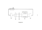
[0007] Um relógio atômico de tipo CPT tem um elemento de laser, uma célula que contém um metal alcalino e um elemento de recebimento de luz para recebimento de luz de laser transmitida através da célula, em que a luz do laser é modulada e duas transições de um elétron em um átomo de metal alcalino são realizadas simultaneamente pelos comprimentos de onda de banda lateral que ocorrem em ambos os lados de uma onda portadora em um comprimento de onda particular para conduzir excitação da mesma. A energia de transição para tal transição é invariável e, quando um comprimento de onda de banda lateral da luz de laser coincide com um comprimento de onda que corresponde à energia de transição, um fenômeno de aumento de transparência ocorre, no qual a taxa de absorção de luz de um metal alcalino é reduzida. Assim, tal relógio atômico é caracterizado pelo fato de que o comprimento de onda de uma onda portadora é ajustado para diminuir a taxa de absorção de luz de um metal alcalino e um sinal detectado pelo elemento de recebimento de luz é alimentado de volta para um modulador, de modo que uma frequência de modulação da luz do laser a partir de um elemento de laser seja ajustada pelo modulador. Adicionalmente, em tal relógio atômico, a luz do laser emitida a partir do elemento de laser irradia sobre uma célula que contém um metal alcalino através de um colimador e uma placa de onda X/4.[0007] A CPT-type atomic clock has a laser element, a cell containing an alkali metal and a light receiving element for receiving laser light transmitted through the cell, wherein the laser light is modulated and two transitions of an electron into an alkali metal atom are carried out simultaneously by sideband wavelengths that occur on both sides of a carrier wave at a particular wavelength to drive excitation thereof. The transition energy for such a transition is invariant and, when a sideband wavelength of laser light coincides with a wavelength that corresponds to the transition energy, a phenomenon of increasing transparency occurs, in which the rate of absorption of light from an alkali metal is reduced. Thus, such an atomic clock is characterized by the fact that the wavelength of a carrier wave is adjusted to decrease the light absorption rate of an alkali metal and a signal detected by the light receiving element is fed back to a modulator. , so that a modulation frequency of laser light from a laser element is adjusted by the modulator. Additionally, in such an atomic clock, laser light emitted from the laser element radiates onto a cell containing an alkali metal through a collimator and an X/4 wave plate.
[0008] Para uma fonte de luz para tal relógio atômico de tipo muito compacto, um laser emissor de superfície compacto com um consumo de energia elétrica muito baixo e uma elevada qualidade de comprimento de onda é adequado e é desejado que a precisão do comprimento de onda de uma onda portadora seja de ± 1 nm em relação a um comprimento de onda particular (por exemplo, Proc. of SPIE Vol. 6132, 613208-1 (2006)).[0008] For a light source for such a very compact type atomic clock, a compact surface emitting laser with a very low electrical power consumption and a high wavelength quality is suitable and the accuracy of the wavelength is desired. wave of a carrier wave is ± 1 nm with respect to a particular wavelength (eg, Proc. of SPIE Vol. 6132, 613208-1 (2006)).
[0009] Entretanto, quando um elemento de laser emissor de superfície é usado para um relógio atômico, pode ser necessário proporcionar um intervalo de comprimento de onda estreito (5 nm) para cada laser emissor de superfície. Consequentemente, uma camada de ajuste de comprimento de onda é formada sobre uma área de ressonador de um laser emissor de superfície e, portanto, quando tal laser emissor de superfície com um intervalo de comprimento de onda estreito é formado, pode ser necessário formar um filme de maneira tal que a espessura de cada filme na camada de ajuste de comprimento de onda seja muito fina. No entanto, pode ser difícil formar um filme de maneira tal que a espessura de cada filme para formação de uma camada de ajuste de comprimento de onda seja extremamente fina e uniforme em virtude de dispersão da taxa de crescimento, irregularidades na distribuição de uma espessura do filme, etc. no momento de formação de uma camada semicondutora.[0009] However, when a surface emitting laser element is used for an atomic clock, it may be necessary to provide a narrow wavelength range (5 nm) for each surface emitting laser. Consequently, a wavelength adjustment layer is formed over a resonator area of a surface emitting laser, and therefore, when such a surface emitting laser with a narrow wavelength range is formed, it may be necessary to form a film. in such a way that the thickness of each film in the wavelength adjustment layer is very thin. However, it can be difficult to form a film in such a way that the thickness of each film for forming a wavelength adjustment layer is extremely thin and uniform due to dispersion of the growth rate, irregularities in the distribution of a thickness of the movie, etc. at formation of a semiconductor layer.
[0010] Especificamente, conforme indicado na Patente Japonesa N° 2751814, quando uma camada de ajuste de comprimento de onda é formada sobre uma área de ressonador e quando um intervalo de comprimento de onda de oscilação pretendido é de 5 nm ou menos, pode ser necessário que a espessura de filme de uma camada de ajuste de comprimento de onda seja de 1,2 nm ou menos, mas pode ser extremamente difícil para a técnica atual de crescimento de cristais de um semicondutor composto controlar tal espessura de filme fino. Assim, mesmo se a espessura de filme é ligeiramente modificada, o comprimento de onda de oscilação pode ser influenciado pela mesma.[0010] Specifically, as indicated in Japanese Patent No. 2751814, when a wavelength adjustment layer is formed over a resonator area and when a desired oscillation wavelength range is 5 nm or less, it can be It is necessary for the film thickness of a wavelength adjustment layer to be 1.2 nm or less, but it can be extremely difficult for the current crystal growth technique of a composite semiconductor to control such thin film thickness. Thus, even if the film thickness is slightly modified, the oscillation wavelength can be influenced by it.
[0011] De acordo com um aspecto da presente invenção, pode ser fornecido um elemento de laser emissor de superfície que inclui um substrato semicondutor e múltiplos lasers emissores de superfície configurados para emitir luz com comprimentos de onda mutuamente diferentes, cada laser emissor de superfície incluindo um refletor de Bragg inferior localizado sobre o substrato semicondutor, um ressonador localizado sobre o refletor de Bragg inferior, um refletor de Bragg superior localizado sobre o ressonador e uma camada de ajuste de comprimento de onda localizada sobre o refletor de Bragg superior ou o refletor de Bragg inferior, as camadas de ajuste de comprimento de onda incluídas nos lasers emissores de superfície tendo espessuras mutuamente diferentes, pelo menos uma das camadas de ajuste de comprimento de onda incluindo camadas de ajuste feitas de dois tipos de materiais e os números das camadas de ajuste incluídas nas camadas de ajuste de comprimento de onda sendo mutuamente diferentes.[0011] According to one aspect of the present invention, there can be provided a surface emitting laser element that includes a semiconductor substrate and multiple surface emitting lasers configured to emit light at mutually different wavelengths, each surface emitting laser including a lower Bragg reflector located over the semiconductor substrate, a resonator located over the lower Bragg reflector, an upper Bragg reflector located over the resonator, and a wavelength adjustment layer located over the upper Bragg reflector or reflector. Lower Bragg, the wavelength adjustment layers included in surface emitting lasers having mutually different thicknesses, at least one of the wavelength adjustment layers including adjustment layers made of two types of materials and the numbers of adjustment layers included in the wavelength adjustment layers being mutually different. tes.
[0012] De acordo com outro aspecto da presente invenção, pode ser fornecido um método para a fabricação de um elemento de laser emissor de superfície que inclui múltiplos lasers emissores de superfície configurados para emitir luz com comprimentos de onda mutuamente diferentes incluindo as etapas de formação de um refletor de Bragg inferior sobre um substrato semicondutor, formação de um ressonador sobre o refletor de Bragg inferior, formação de um refletor de Bragg superior sobre o ressonador, laminação de camadas de ajuste feitas de dois tipos de materiais sobre o refletor de Bragg superior ou o refletor de Bragg inferior para formar uma camada de ajuste de comprimento de onda, remoção de uma camada de ajuste na camada de ajuste de comprimento de onda usando um primeiro fluido de decapagem e remoção de outra camada de ajuste na camada de ajuste de comprimento de onda usando um segundo fluido de decapagem diferente do primeiro fluido de decapagem, de modo que as camadas de ajuste de comprimento de onda incluídas nos lasers emissores de superfície tenham espessuras mutuamente diferentes e os números das camadas de ajuste incluídas nas camadas de ajuste de comprimento de onda sejam mutuamente diferentes.[0012] According to another aspect of the present invention, there can be provided a method for manufacturing a surface emitting laser element that includes multiple surface emitting lasers configured to emit light at mutually different wavelengths including the forming steps of a lower Bragg reflector over a semiconductor substrate, forming a resonator over the lower Bragg reflector, forming an upper Bragg reflector over the resonator, laminating adjustment layers made of two types of materials onto the upper Bragg reflector or the lower Bragg reflector to form a wavelength adjustment layer, removing an adjustment layer in the wavelength adjustment layer using a first pickling fluid and removing another adjustment layer in the length adjustment layer waveform using a second blasting fluid different from the first blasting fluid, so that the adjustment layers of c. The wavelengths included in the surface emitting lasers have mutually different thicknesses and the numbers of adjustment layers included in the wavelength adjustment layers are mutually different.
[0013] De acordo com outro aspecto da presente invenção, pode ser fornecido um oscilador atômico que inclui o elemento de laser emissor de superfície conforme descrito acima, uma célula de metal alcalino que inclui um metal alcalino a ser irradiado com a luz emitida a partir do elemento de laser emissor de superfície, um fotodetector configurado para detectar luz que foi transmitida através da célula de metal alcalino e um controlador configurado para controlar a frequência de oscilação do elemento de laser emissor de superfície com base na luz detectada pelo fotodetector.[0013] According to another aspect of the present invention, there may be provided an atomic oscillator that includes the surface emitting laser element as described above, an alkali metal cell that includes an alkali metal to be irradiated with light emitted from of the surface emitting laser element, a photodetector configured to detect light that has been transmitted through the alkali metal cell, and a controller configured to control the frequency of oscillation of the surface emitting laser element based on the light detected by the photodetector.
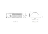
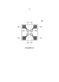
[0014] A Figura 1 é uma vista superior de um elemento de laser emissor de superfície em uma primeira concretização.[0014] Figure 1 is a top view of a surface emitting laser element in a first embodiment.
[0015] A Figura 2 é um diagrama que ilustra um elemento de laser emissor de superfície em uma primeira concretização.[0015] Figure 2 is a diagram illustrating a surface emitting laser element in a first embodiment.
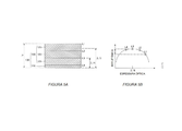
[0016] A Figura 3 é um diagrama estrutural de uma camada de ajuste de comprimento de onda de um elemento de laser emissor de superfície em uma primeira concretização.[0016] Figure 3 is a structural diagram of a wavelength adjustment layer of a surface emitting laser element in a first embodiment.
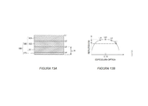
[0017] A Figura 4A e a Figura 4B são diagramas que ilustram (1) uma camada de ajuste de comprimento de onda de um elemento de laser emissor de superfície em uma primeira concretização.[0017] Figure 4A and Figure 4B are diagrams illustrating (1) a wavelength adjustment layer of a surface emitting laser element in a first embodiment.
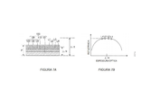
[0018] A Figura 5A e a Figura 5B são diagramas que ilustram (2) uma camada de ajuste de comprimento de onda de um elemento de laser emissor de superfície em uma primeira concretização.[0018] Figure 5A and Figure 5B are diagrams illustrating (2) a wavelength adjustment layer of a surface emitting laser element in a first embodiment.
[0019] A Figura 6A e a Figura 6B são diagramas que ilustram (3) uma camada de ajuste de comprimento de onda de um elemento de laser emissor de superfície em uma primeira concretização.[0019] Figure 6A and Figure 6B are diagrams illustrating (3) a wavelength adjustment layer of a surface emitting laser element in a first embodiment.
[0020] A Figura 7A e a Figura 7B são diagramas que ilustram (4) uma camada de ajuste de comprimento de onda de um elemento de laser emissor de superfície em uma primeira concretização.[0020] Figure 7A and Figure 7B are diagrams illustrating (4) a wavelength adjustment layer of a surface emitting laser element in a first embodiment.
[0021] A Figura 8 é um diagrama que ilustra (5) uma camada de ajuste de comprimento de onda de um elemento de laser emissor de superfície em uma primeira concretização.[0021] Figure 8 is a diagram illustrating (5) a wavelength adjustment layer of a surface emitting laser element in a first embodiment.
[0022] A Figura 9 é um diagrama que ilustra (6) uma camada de ajuste de comprimento de onda de um elemento de laser emissor de superfície em uma primeira concretização.[0022] Figure 9 is a diagram illustrating (6) a wavelength adjustment layer of a surface emitting laser element in a first embodiment.
[0023] A Figura 10 é uma vista superior de um elemento de laser emissor de superfície em uma segunda concretização.[0023] Figure 10 is a top view of a surface emitting laser element in a second embodiment.
[0024] A Figura 11 é um diagrama que ilustra um elemento de laser emissor de superfície em uma segunda concretização.[0024] Figure 11 is a diagram illustrating a surface emitting laser element in a second embodiment.
[0025] A Figura 12A e a Figura 12B são diagramas que ilustram (1) uma camada de ajuste de um comprimento de onda de um elemento de laser emissor de superfície em uma segunda concretização.[0025] Figure 12A and Figure 12B are diagrams illustrating (1) a wavelength adjustment layer of a surface emitting laser element in a second embodiment.
[0026] A Figura 13A e a Figura 13B são diagramas que ilustram (2) uma camada de ajuste de comprimento de onda de um elemento de laser emissor de superfície em uma segunda concretização.[0026] Figure 13A and Figure 13B are diagrams illustrating (2) a wavelength adjustment layer of a surface emitting laser element in a second embodiment.
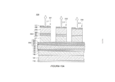
[0027] A Figura 14 é uma vista superior de um elemento de laser emissor de superfície em uma terceira concretização.[0027] Figure 14 is a top view of a surface emitting laser element in a third embodiment.
[0028] A Figura 15A e a Figura 15B são diagramas que ilustram um elemento de laser emissor de superfície em uma terceira concretização.[0028] Figure 15A and Figure 15B are diagrams illustrating a surface emitting laser element in a third embodiment.
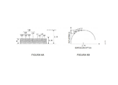
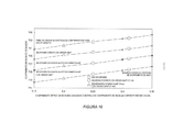
[0029] A Figura 16 é um diagrama de correlação entre uma primeira camada de ajuste de comprimento de onda e uma segunda camada de ajuste de comprimento de onda e um comprimento de onda de oscilação.[0029] Figure 16 is a correlation diagram between a first wavelength adjustment layer and a second wavelength adjustment layer and an oscillating wavelength.
[0030] A Figura 17A e a Figura 17B são diagramas que ilustram (1) uma primeira camada de ajuste de comprimento de onda de um elemento de laser emissor de superfície de uma terceira concretização.[0030] Figure 17A and Figure 17B are diagrams illustrating (1) a first wavelength adjustment layer of a surface emitting laser element of a third embodiment.
[0031] A Figura 18A e a Figura 18B são diagramas que ilustram (2) uma primeira camada de ajuste de comprimento de onda de um elemento de laser emissor de superfície de uma terceira concretização.[0031] Figure 18A and Figure 18B are diagrams illustrating (2) a first wavelength adjustment layer of a surface emitting laser element of a third embodiment.
[0032] A Figura 19A e a Figura 19B são diagramas que ilustram (3) uma primeira camada de ajuste de comprimento de onda de um elemento de laser emissor de superfície de uma terceira concretização.[0032] Figure 19A and Figure 19B are diagrams illustrating (3) a first wavelength adjustment layer of a surface emitting laser element of a third embodiment.
[0033] A Figura 20 é uma vista superior de um elemento de laser emissor de superfície em uma quarta concretização.[0033] Figure 20 is a top view of a surface emitting laser element in a fourth embodiment.
[0034] A Figura 21 é um diagrama estrutural de um oscilador atômico em uma quinta concretização.[0034] Figure 21 is a structural diagram of an atomic oscillator in a fifth embodiment.
[0035] A Figura 22 é um diagrama que ilustra o nível de energia atômica para ilustrar um tipo CPT.[0035] Figure 22 is a diagram illustrating the atomic energy level to illustrate a CPT type.
[0036] A Figura 23 é um diagrama que ilustra um comprimento de onda de saída no momento de modulação de um laser emissor de superfície.[0036] Figure 23 is a diagram illustrating an output wavelength at the time of modulation of a surface emitting laser.
[0037] A Figura 24 é um diagrama de correlação entre a frequência de modulação e a quantidade de luz transmitida.[0037] Figure 24 is a correlation diagram between the modulation frequency and the amount of transmitted light.
[0038] Concretização(ões) da presente invenção será(ão) descrita(s) a seguir. Além disso, números de referência idênticos serão aplicados a elementos idênticos, etc., e (uma) descrição(ões) dos mesmos será(ão) omitida(s).[0038] Embodiment(s) of the present invention will be described below. In addition, identical reference numbers will apply to identical elements, etc., and (a) description(s) thereof will be omitted.
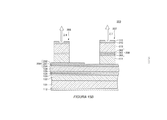
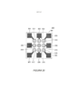
[0039] Um elemento de laser emissor de superfície em uma primeira concretização será descrito. Conforme ilustrado na Figura 1 e Figura 2A, um elemento de laser emissor de superfície 10 na presente concretização tem múltiplos lasers de emissão de superfície e, especificamente, tem um primeiro laser emissor de superfície 11, um segundo laser emissor de superfície 12, um terceiro laser emissor de superfície 13 e um quarto laser emissor de superfície 14. Adicionalmente, a Figura 1 foi simplificada por uma questão de explicação da presente concretização, em que a representação de uma camada de contato, etc., foi convenientemente omitida. Além disso, a Figura 2 é um diagrama em seção transversal fornecido ao cortar ao longo de uma linha pontilhada/tracejada 1A-1B na Figura 1.[0039] A surface emitting laser element in a first embodiment will be described. As illustrated in Figure 1 and Figure 2A, a surface
[0040] O elemento de laser emissor de superfície 10 na presente concretização é formado sobre um chip semicondutor de 300 μm quadrados, em que cada um do primeiro laser emissor de superfície 11, segundo laser emissor de superfície 12, terceiro laser emissor de superfície 13 e quarto laser emissor de superfície 14 formados sobre tal chip semicondutor está conectado a um bloco de eletrodos fornecido para corresponder aos mesmos. Especificamente, um bloco de eletrodo 21 está conectado ao primeiro laser emissor de superfície 11 e um bloco de eletrodo 22 está conectado ao segundo laser emissor de superfície 12, enquanto que um bloco de eletrodo 23 está conectado ao terceiro laser emissor de superfície 13 e um bloco de eletrodo 24 está conectado ao quarto laser emissor de superfície 14.[0040] The surface emitting
[0041] Além disso, o primeiro laser emissor de superfície 11, o segundo laser emissor de superfície 12, o terceiro laser emissor de superfície 13 e o quarto laser emissor de superfície 14 fornecem luz emitida com comprimentos de onda mutuamente diferentes. Ou seja, um comprimento de onda A.1 emitido a partir do primeiro laser emissor de superfície 11, um comprimento de onda A.2 emitido a partir do segundo laser emissor de superfície 12, um comprimento de onda A.3 emitido a partir do terceiro laser emissor de superfície 13 e um comprimento de onda À.4 emitido a partir do quarto laser emissor de superfície 14 são comprimentos de onda mutuamente diferentes.[0041] Furthermore, the first
[0042] Adicionalmente, o elemento de laser emissor de superfície, na presente concretização, é para obter um laser emissor de superfície com um comprimento de onda de oscilação de 894,6 nm, em que quatro lasers emissores de superfície são formados sobre um chip semicondutor (substrato) de 300 μm quadrados. Uma vez que pode ser possível formar múltiplos lasers emissores de superfície em uma área estreita em um elemento de laser emissor de superfície, há pouca alteração na posição do ponto de emissão de luz, mesmo quando um laser emissor de superfície para conduzir a emissão de luz é ligado. Portanto, um tamanho de substrato é um tamanho de 500 μm x 500 μm ou menos, no qual ajuste do eixo óptico, etc., pode ser desnecessário ou extremamente facilitado.[0042] Additionally, the surface emitting laser element, in the present embodiment, is to obtain a surface emitting laser with an oscillating wavelength of 894.6 nm, wherein four surface emitting lasers are formed on a chip. 300 µm square semiconductor (substrate). Since it may be possible to form multiple surface emitting lasers in a narrow area on a surface emitting laser element, there is little change in the position of the light emitting point, even when a surface emitting laser to conduct light emission is turned on. Therefore, a substrate size is a size of 500 µm x 500 µm or less, in which adjustment of the optical axis, etc., may be unnecessary or extremely facilitated.
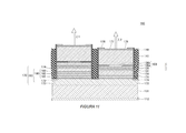
[0043] Para o elemento de laser emissor de superfície na presente concretização, materiais semicondutores com diferentes índices de refração são alternadamente laminados sobre e formados sobre um substrato 101 feito de um semicondutor, etc., para formar um refletor de Bragg inferior 102, e uma camada espaçadora inferior 103, uma camada ativa 104 e uma camada espaçadora superior 105 são formadas sobre o refletor de Bragg inferior 102. Um primeiro refletor de Bragg superior 106, uma camada de contato 110, uma área de ajuste de comprimento de onda 120 e um segundo refletor de Bragg superior 107 são formados sobre a camada espaçadora superior 105. Além disso, um eletrodo superior 111 é formado sobre e conectado à camada de contato 110 e um eletrodo inferior 112 é formado sobre uma face posterior do substrato 101. Embora a camada de ajuste de comprimento de onda 130 seja constituída pela camada de contato 110 e a área de ajuste de comprimento de onda 120 na presente concretização, a camada de ajuste de comprimento de onda 130 pode ser constituída apenas por uma área de ajuste de comprimento de onda 120 em um caso onde a camada de contato 110 não é formada adjacente à área de ajuste de comprimento de onda 120. Adicionalmente, o refletor de Bragg inferior 102, camada espaçadora inferior 103, camada ativa 104, camada espaçadora superior 105, primeiro refletor de Bragg superior 106, camada de contato 110 e área de ajuste de comprimento de onda 120, as quais são camadas semicondutoras formadas sobre o substrato 101, são formados por materiais semicondutores de crescimento epitaxial. Especificamente, tais camadas semicondutoras são formadas por crescimento epitaxial em Depósito de Vapor Químico sobre Metal Orgânico (Metal Organic Chemical Vapor Deposition - MOCVD) ou Epitaxia por Feixes Moleculares (Molecular Beam Epitaxy - MBE). Além disso, um refletor de Bragg conforme descrito no relatório descritivo para o presente pedido de patente pode ser descrito como um refletor de Bragg distribuído (Distributed Bragg Reflector - DBR).[0043] For the surface emitting laser element in the present embodiment, semiconductor materials with different refractive indices are alternately laminated onto and formed on a
[0044] Além disso, o segundo refletor de Bragg superior 107 é formado sobre a camada de ajuste de superfície. O segundo refletor de Bragg superior 107 é um filme dielétrico feito de um óxido, nitreto, fluoreto, etc., e formado ao laminar e moldar alternadamente (um) filme(s) de material de elevado índice de refração e (um) filme(s) de material de baixo índice de refração. Além disso, um refletor de Bragg superior é constituído pelo primeiro refletor de Bragg superior 106, a camada de ajuste de comprimento de onda 130 e o segundo refletor de Bragg superior 107 na presente concretização. Além disso, a camada de ajuste de comprimento de onda 130 pode ser formada dentro do refletor de Bragg inferior 102.[0044] In addition, the second
[0045] No elemento de laser emissor de superfície na presente concretização, as espessuras das áreas de ajuste de comprimento de onda 120 nas camadas de ajuste de comprimento de onda 130 no primeiro laser emissor de superfície 11, segundo laser emissor de superfície 12, terceiro laser emissor de superfície 13 e quarto laser emissor de superfície 14 são diferentes umas das outras. Especificamente, conforme ilustrado na Figura 3, a área de ajuste de comprimento de onda 120 é formada sobre a camada de contato 110, em que a área de ajuste de comprimento de onda 120 é constituída por uma primeira camada de ajuste 121, uma segunda camada de ajuste 122 e uma terceira camada de ajuste 123. Na presente concretização, a primeira camada de ajuste 121 e a terceira camada de ajuste 123 são feitas de GaInP, enquanto que a segunda camada de ajuste 122 é feita de GaAsP. Adicionalmente, materiais para fazer a primeira camada de ajuste 121, segunda camada de ajuste 122 e terceira camada de ajuste 123 podem ser opostos a isso.[0045] In the surface emitting laser element in the present embodiment, the thicknesses of the
[0046] Assim, as espessuras das áreas de ajuste de comprimento de onda 120 no primeiro laser emissor de superfície 11, segundo laser emissor de superfície 12, terceiro laser emissor de superfície 13 e quarto laser emissor de superfície 14 são diferentes no elemento de laser emissor de superfície na presente concretização.[0046] Thus, the thicknesses of the
[0047] Especificamente, a primeira camada de ajuste 121, a segunda camada de ajuste 122 e a terceira camada de ajuste 123 são formadas sobre a área de ajuste de comprimento de onda 120 no primeiro laser emissor de superfície 11, em que luz com um comprimento de onda A.1 é emitida, a qual corresponde a uma espessura da camada de ajuste de comprimento de onda 130 que é uma soma de tal área de ajuste de comprimento de onda 120 e da camada de contato 110.[0047] Specifically, the
[0048] Além disso, a primeira camada de ajuste 121 e a segunda camada de ajuste 122 são formadas na área de ajuste de comprimento de onda 120 no segundo laser emissor de superfície 12, em que luz com um comprimento de onda A.2 é emitida, a qual corresponde a uma espessura da camada de ajuste de comprimento de onda 130, que é uma soma de tal área de ajuste de comprimento de onda 120 e da camada de contato 110.[0048] Furthermore, the
[0049] Além disso, a primeira camada de ajuste 121 é formada na área de ajuste de comprimento de onda 120 no terceiro laser emissor de superfície 13, em que luz com um comprimento de onda A.3 é emitida, a qual corresponde a uma espessura da camada de ajuste de comprimento de onda 130 que é uma soma de tal área de ajuste de comprimento de onda 120 e da camada de contato 110.[0049] Furthermore, the
[0050] Além disso, a área de ajuste de comprimento de onda 120 não é formada no quarto laser emissor de superfície 14 e, consequentemente, luz com um comprimento de onda A.4 é emitida, a qual corresponde a uma espessura da camada de ajuste de comprimento de onda 130 que é igual à espessura da camada de contato 110.[0050] Furthermore, the
[0051] Assim, pode ser possível alterar a espessura das camadas de ajuste de comprimento de onda 130 no primeiro laser emissor de superfície 11, segundo laser emissor de superfície 12, terceiro laser emissor de superfície 13 e quarto laser emissor de superfície 14 pouco a pouco, e pode ser possível emitir luz com cada comprimento de onda que corresponde a uma espessura de pelo menos uma ou cada uma das camadas de ajuste de comprimento de onda 130.[0051] Thus, it may be possible to change the thickness of the wavelength adjustment layers 130 in the first
[0052] Na presente concretização, um substrato de n-GaAs é usado para o substrato 101. Além disso, o refletor de Bragg inferior 102 é formado ao laminar 35,5 pares de uma camada de n-Al0,1Ga0,9As de elevado índice de refração e uma camada de n-Al0,9Ga0,1As de baixo índice de refração, de maneira tal que a espessura óptica do filme de cada camada seja de X/4.[0052] In the present embodiment, an n-GaAs substrate is used for
[0053] A camada ativa 104 constituída por uma camada de cavidade quantum de GaInAs/camada de barreira de GaInPAs é formada sobre o refletor de Bragg inferior 102 através da camada espaçadora inferior 103 feita de Al0,2Ga0,8As. A camada espaçadora superior 105 feita de Al0,2Ga0,8As e o primeiro refletor de Bragg superior 106 são formados sobre a camada ativa 104. Adicionalmente uma área de ressonador dotada de uma espessura óptica de um comprimento de onda é constituída pela camada espaçadora inferior 103, a camada ativa 104 e a camada espaçadora superior 105.[0053] The
[0054] O primeiro refletor de Bragg superior 106 é formado ao laminar 6 pares de uma camada de n-Al0,1Ga0,9As de elevado índice de refração e camada de n-Al0,9Ga0,1As de baixo índice de refração, de maneira tal que a espessura óptica de filme de cada camada seja A./4. Uma das camadas de baixo índice de refração do primeiro refletor de Bragg superior 106 é constituída por uma camada de estreitamento de corrente elétrica 108 feita de AlAs, em que uma porção periférica da camada de estreitamento de corrente elétrica 108 é seletivamente oxidada para formar uma área de oxidação seletiva 108a e uma área de estreitamento de corrente elétrica 108b não oxidada é formada sobre uma porção central da mesma.[0054] The first
[0055] A camada de contato 110 feita de p-GaAs e a área de ajuste de comprimento de onda 120 constituída pela primeira camada de ajuste 121, segunda camada de ajuste 122 e terceira camada de ajuste 123 são formadas sobre o primeiro refletor de Bragg superior 106. Além disso, uma parte das camadas na área de ajuste de comprimento de onda 120 é removida para corresponder a um comprimento de onda emitido a partir de cada laser emissor de superfície, conforme descrito acima.[0055] The
[0056] Cada laser emissor de superfície de um elemento de laser emissor de superfície na presente concretização tem uma mesa estrutura, em que uma tal mesa estrutura é formada ao remover uma camada semicondutora entre os lasers emissores de superfície a serem formados em virtude de decapagem. Após uma mesa estrutura ser formada, tratamento térmico em vapor de água é realizado para oxidar a camada de estreitamento de corrente elétrica 108 a partir de uma periferia da mesa estrutura, pelo que a área de oxidação seletiva 108a (uma área oxidada) sobre uma porção periférica e a área de estreitamento de corrente elétrica não oxidada 108b sobre uma porção central são formadas. Isto é, a camada de estreitamento de corrente elétrica 108 é constituída pela área de oxidação seletiva oxidada 108a e a área de estreitamento de corrente elétrica não oxidada 108b para proporcionar uma estrutura de estreitamento de corrente elétrica. Adicionalmente, o formato, visto a partir de cima da mesa estrutura, pode ser formado para ter um formato circular ou pode ser formado para ter um formato tal como um formato elíptico, um formato quadrado ou um formato retangular.[0056] Each surface emitting laser of a surface emitting laser element in the present embodiment has a table structure, wherein such a table structure is formed by removing a semiconductor layer between the surface emitting lasers to be formed by virtue of etching . After a table structure is formed, heat treatment in water vapor is carried out to oxidize the electrical
[0057] Além disso, o segundo refletor de Bragg superior 107 é formado sobre a camada de ajuste de comprimento de onda 130, em que remoção que corresponde a cada laser emissor de superfície é realizada por meio de decapagem. O segundo refletor de Bragg superior 107 é formado ao laminar 8,5 pares de uma camada de TiO2 de elevado índice de refração e uma camada de SiO2 de baixo índice de refração, de maneira tal que a espessura de filme óptico de cada camada seja A./4. Além disso, pode ser necessário que apenas o segundo refletor de Bragg superior 107 seja feito de (um) material(is) dielétrico(s) e formado ao laminar um material de elevado índice de refração e um material de baixo índice de refração, em que pode ser possível fornecer um material, tal como um óxido, um nitreto ou um fluoreto, especificamente. Para um material de elevado índice de refração, pode ser possível fornecer Ta2O5, HfO2, etc., bem como TiO2. Além disso, para um material de baixo índice de refração, pode ser possível fornecer MgF2, etc., bem como SiO2. Para um método para formação de uma camada de TiO2 de elevado índice de refração e uma camada de SiO2 de baixo índice de refração no segundo refletor de Bragg superior 107, a formação é realizada por meio de pulverização catódica ou deposição a vácuo, etc. Além disso, um filme protetor 140 feito de SiN é formado em geral e um filme de resina 141 feito de um material de resina, tal como uma poli-imida, é formado entre mesas dos respectivos lasers emissores de superfície.[0057] Furthermore, the second
[0058] Depois disso, um eletrodo superior 111 é formado, o qual é um eletrodo do p-lado. Tal eletrodo superior 111 é formado para corresponder a cada laser emissor de superfície, em que cada eletrodo superior 111 está conectado a cada um dos blocos de eletrodo 21 - 24. Além disso, um eletrodo inferior 112, o qual é um eletrodo do n-lado, é formado sobre uma face posterior do substrato 101.[0058] After that, an
[0059] Em seguida, um método para formação da camada de ajuste de comprimento de onda 130 no elemento de laser emissor de superfície na presente concretização será descrito em detalhes.[0059] Next, a method for forming the
[0060] Primeiro, o refletor de Bragg inferior 102, camada espaçadora inferior 103, camada ativa 104, camada espaçadora superior 105, primeiro refletor de Bragg superior 106, camada de contato 110 e uma área de ajuste de comprimento de onda 120, as quais são feitas de materiais semicondutores, são formadas sobre o substrato 101 por meio de crescimento epitaxial em MOCVD ou MBE. Adicionalmente, a camada de ajuste de comprimento de onda 130 é constituída pela camada de contato 110 e uma área de ajuste de comprimento de onda 120, em que a área de ajuste de comprimento de onda 120 é formada ao laminar a primeira camada de ajuste 121, a segunda camada de ajuste 122 e a terceira camada de ajuste 123. Aqui, conforme mencionado acima, a primeira camada de ajuste 121 e a terceiro camada de ajuste 123 são feitas de GaInP, enquanto que a segunda camada de ajuste 122 é feita de GaAsP.[0060] First, the
[0061] Então, um padrão de resistor é formado sobre uma área na qual o primeiro laser emissor de superfície 11 é formado. Especificamente, um padrão de resistor é formado mediante aplicação de um fotoresistor sobre a terceira camada de ajuste 123 na área de ajuste de comprimento de onda 120 e realização de exposição à luz e revelação do mesmo por um dispositivo de exposição à luz.[0061] Then, a resistor pattern is formed over an area in which the first
[0062] Então, a terceira camada de ajuste 123 sobre uma área na qual nenhum padrão de resistor foi formado é removida por meio de decapagem a úmido. Especificamente, decapagem a úmido é realizada por um fluido misto de ácido clorídrico e água, uma vez que a terceira camada de ajuste 123 é feita de GaInP. Deste modo, apenas a terceira camada de ajuste 123 em uma área sobre a qual nenhum padrão de resistor tenha sido formado é removida para expor uma superfície da segunda camada de ajuste 122. Além disso, pode ser possível que tal fluido misto seja usado para realizar a decapagem do GaInP que constitui a terceira camada de ajuste 123, mas dificilmente pode ser possível realizar decapagem do GaAsP que constitui a segunda camada de ajuste 122. Tal fluido misto pode também ser descrito como um primeiro fluido de decapagem. Depois disso, o padrão de resistor é removido por um solvente orgânico, etc.[0062] Then, the
[0063] Então, um padrão de resistor é formado sobre uma área na qual o primeiro laser emissor de superfície 11 e o segundo laser emissor de superfície 12 são formados. Especificamente, um padrão de resistor é formado mediante aplicação de um fotoresistor sobre a terceira camada de ajuste 123 e a segunda camada de ajuste 122 sobre a área de ajuste de comprimento de onda 120 e realizando exposição à luz e revelação do mesmo por um dispositivo de exposição à luz.[0063] Then, a resistor pattern is formed over an area in which the first
[0064] Então, a segunda camada de ajuste 122 sobre uma área na qual nenhum padrão de resistor foi formado é removida por meio de decapagem a úmido. Especificamente, decapagem a úmido é realizada por um fluido misto de ácido sulfúrico, peróxido de hidrogênio e água, uma vez que a segunda camada de ajuste 122 é feita de GaAsP. Deste modo, apenas a segunda camada de ajuste 122 em uma área na qual nenhum padrão de resistor tenha sido formado é removida para expor uma superfície da primeira camada de ajuste 121. Além disso, pode ser possível que tal fluido misto seja usado para decapagem do GaAsP que constitui a segunda camada de ajuste 122, mas dificilmente pode ser possível realizar decapagem do GaInP que constitui a primeira camada de ajuste 121. Tal fluido misto pode ser descrito como um segundo fluido de decapagem. Depois disso, o padrão de resistor é removido por um solvente orgânico, etc.[0064] Then, the
[0065] Então, um padrão de resistor é formado sobre uma área na qual o primeiro laser emissor de superfície 11, o segundo laser emissor de superfície 12 e o terceiro laser emissor de superfície 13 são formados. Especificamente, um padrão de resistor é formado mediante aplicação de um fotoresistor sobre a primeira camada de ajuste 121, a segunda camada de ajuste 122 e a terceira camada de ajuste 123 na área de ajuste de comprimento de onda 120 e realizando exposição à luz e revelação do mesmo por um dispositivo de exposição à luz.[0065] Then, a resistor pattern is formed over an area in which the first
[0066] Em seguida, a primeira camada de ajuste 121 em uma área sobre a qual nenhum padrão de resistor foi formado é removida por meio de decapagem a úmido. Especificamente, a primeira camada de ajuste 121 em uma área sobre a qual nenhum padrão de resistor tenha sido formado é removida pelo primeiro fluido de decapagem. Deste modo, apenas a primeira camada de ajuste 121 em uma área sobre a qual nenhum padrão de resistor tenha sido formado é removida para expor uma superfície da camada de contato 110. Depois disso, o padrão de resistor é removido por um solvente orgânico, etc.[0066] Next, the
[0067] Então, o segundo refletor de Bragg superior 107 é formado. Especificamente, a formação é realizada ao laminar alternadamente um filme dielétrico feito de um material de elevado índice de refração e um filme dielétrico feito de um material de baixo índice de refração, os quais são compostos de um óxido, um nitreto, um fluoreto, etc., com cada um tendo uma espessura de filme predeterminada em virtude de pulverização catódica, etc. Além disso, também pode ser possível formar o segundo refletor de Bragg superior 107 por meio de laminação e moldagem de materiais semicondutores tendo índices de refração diferentes.[0067] Then, the second
[0068] Desse modo, pode ser possível formar a camada de ajuste de comprimento de onda 130 e segundo refletor de Bragg superior 107 no elemento de laser emissor de superfície na presente concretização.[0068] Thereby, it may be possible to form the
[0069] Na presente concretização, Al não está incluído em qualquer uma da primeira camada de ajuste 121, segunda camada de ajuste 122 e terceira camada de ajuste 123 que constituem a área de ajuste de comprimento de onda 120 na camada de ajuste de comprimento de onda 130 e, portanto, oxidação, etc. dificilmente ocorrem após decapagem, pelo que pode ser possível manter uma condição de superfície limpa após decapagem. Ou seja, pode ser extremamente fácil que o Al sofra corrosão e, portanto, quando uma da primeira camada de ajuste 121, segunda camada de ajuste 122 e terceira camada de ajuste 123 é formada por um material que inclui Al, o estado da superfície após realização de decapagem a úmido, etc. pode ser pobre em que, mesmo embora o segundo refletor de Bragg superior 107 seja formado sobre a mesma, delaminação da mesma pode ocorrer ou uma espessura sua pode ser não homogênea. No entanto, a área de ajuste de comprimento de onda 120 no elemento de laser emissor de superfície na presente concretização é formada por um material que não inclui Al e, portanto, corrosão de Al, etc. não ocorre e tal problema não pode ocorrer.[0069] In the present embodiment, Al is not included in any of the
[0070] Além disso, a área de ajuste de comprimento de onda 120 na camada de ajuste de comprimento de onda 130 na presente concretização é feita de GaAsP e GaInP alternados e, quando decapagem a úmido é conduzida usando dois tipos de fluidos de decapagem, pode ser mutuamente possível realizar uma decapagem dos mesmos e pode não ser possível realizar decapagem de outra. A decapagem é realizada usando dois tipos de tais fluidos de decapagem, pelo que a superfície após decapagem pode ser plana e pode ser possível realizar a moldagem com uma espessura predeterminada sem decapagem excessiva. Deste modo, pode ser possível obter um elemento de laser emissor de superfície com uma característica estável.[0070] In addition, the
[0071] Adicionalmente, embora um caso de uma combinação de GaAsP e GaInP tenha sido descrito na(s) descrição(ões) para a presente concretização, pode ser fornecida uma combinação com outro material que não inclui Al, para o qual é ainda fornecido um fluido de decapagem diferente e é um material semicondutor com uma energia de amplitude de banda maior do que um comprimento de onda de oscilação. Para 894,6 nm, o qual é um comprimento de onda de oscilação na presente concretização é fornecido, por exemplo, GaInAsP/GaInP, GaAs/GaInP, GaAs /GaInAsP, GaAsP/GaInAsP, etc., como uma combinação de tais materiais semicondutores. Além disso, N ou Sb pode ser adicionado aos mesmos, tal como GaAsN/GaInP, GaInNAs/GaInP, GaAsSb/GaInP, etc.[0071] Additionally, although a case of a combination of GaAsP and GaInP has been described in the description(s) for the present embodiment, a combination with other material that does not include Al may be provided, for which it is further provided a different pickling fluid and is a semiconductor material with a band amplitude energy greater than an oscillating wavelength. For 894.6 nm, which is an oscillating wavelength in the present embodiment, for example, GaInAsP/GaInP, GaAs/GaInP, GaAs /GaInAsP, GaAsP/GaInAsP, etc. are provided as a combination of such semiconductor materials . Furthermore, N or Sb can be added to them, such as GaAsN/GaInP, GaInNAs/GaInP, GaAsSb/GaInP, etc.
[0072] Conforme descrito acima, pode ser possível formar múltiplos lasers emissores de superfície para emitir luz com comprimentos de onda diferentes sobre um substrato 101 no elemento de laser emissor de superfície na presente concretização. Desse modo, mesmo que uma variação na espessura de filme de uma camada semicondutora, etc. ocorra na fabricação de um elemento de laser emissor de superfície, uma emissão de luz com um comprimento de onda mais próximo de um comprimento de onda desejado é selecionada dentre o primeiro laser 11 ao quarto laser emissor de superfície 14, pelo que pode ser possível obter um laser semicondutor com um comprimento de onda desejado com facilidade. Deste modo, pode ser possível fabricar um elemento de laser emissor de superfície tendo um laser emissor de superfície que emite luz com um comprimento de onda predeterminado em um baixo custo.[0072] As described above, it may be possible to form multiple surface emitting lasers to emit light with different wavelengths onto a
[0073] Adicionalmente, quando a camada de contato 110 é formada sobre a área de ajuste de comprimento de onda 120, uma quantidade de corrente elétrica capaz de fluir em cada laser emissor de superfície, etc. é variada de acordo com a espessura da área de ajuste de comprimento de onda 120 e uma característica elétrica e característica de emissão de luz de cada laser emissor de superfície também podem ser grandemente diferentes. Além disso, quando a corrente elétrica flui na área de ajuste de comprimento de onda 120, uma resistência elétrica pode ser aumentada por uma descontinuidade de banda em uma interface de cada camada. Contudo, a camada de contato 110 é formada sob a área de ajuste de comprimento de onda 120 no elemento de laser emissor de superfície na presente concretização, pelo que a corrente elétrica injetada no laser emissor de superfície não pode passar através da área de ajuste de comprimento de onda 120 e a resistência, etc. não pode ser alterada dependendo da espessura da área de ajuste de comprimento de onda 120.[0073] Additionally, when the
[0074] Em seguida, uma vantagem do primeiro refletor de Bragg superior 106 formado entre a camada de ajuste de comprimento de onda 130 e uma área de ressonador será descrita. Por exemplo, quando uma camada de ajuste de comprimento de onda é formada em uma área de ressonador tendo um comprimento óptico de um comprimento de onda e quando quatro comprimentos de onda são fornecidos com um comprimento de onda central de 895 nm e um intervalo de comprimento de 1 nm, a camada que constitui a camada de ajuste de comprimento de onda é fornecida com 1,3 nm, em que pode ser extremamente difícil realizar moldagem uniforme sobre uma superfície de pastilha com uma técnica de crescimento de cristal atual. Assim, o primeiro refletor de Bragg superior 106, o qual é uma parte do refletor de Bragg superior, é formado entre a área do ressonador e a camada de ajuste de comprimento de onda 130 na presente concretização. Especificamente, o primeiro refletor de Bragg superior 106 é formado ao laminar 6 pares de uma camada de n-Al0,1Ga0,9As de elevado índice de refração e uma camada de n-Al0,9Ga0,1As de baixo índice de refração de maneira tal que a espessura óptica de filme de cada camada seja À./4. Além disso, a camada de contato 110 é formada sobre o primeiro refletor de Bragg superior 106 e a área de ajuste de comprimento de onda 120 é formada sobre a camada de contato 110. A primeira camada de ajuste 121, segunda camada de ajuste 122 e terceira camada de ajuste 123 que constituem a área de ajuste de comprimento de onda 120 são formadas de maneira tal que a espessura dos filmes de GaInP/GaAsP/GaInP são de 16 nm/ 16 nm/16 nm, respectivamente, em que pode ser possível realizar fabricação suficientemente uniforme com uma técnica de crescimento de cristal atual. Assim, pode ser possível reduzir desvios do intervalo de comprimento de onda entre os lasers emissores de superfície.[0074] Next, an advantage of the upper
[0075] Além disso, também pode ser possível reduzir a resistência elétrica simultaneamente ao formar tal estrutura. Isto é, o segundo refletor de Bragg superior 107, o qual é um dielétrico, é formado por cima da camada de ajuste de comprimento de onda 130 e o eletrodo superior 111 é formado em uma adjacência da mesma em que, quando uma camada de ajuste de comprimento de onda é fornecida em uma área de ressonador, pode ser necessário fornecer uma camada de AlAs que é seletivamente oxidada em uma posição próxima de uma camada de contato em vista da estrutura de camadas e o canal de corrente elétrica pode ser estreitado para aumentar a resistência elétrica. Aqui, o primeiro refletor de Bragg superior 106 é formado entre a camada de ajuste de comprimento de onda 130 (em que a camada de contato 110 é formada sob a área de ajuste de comprimento de onda 120) e a área do ressonador na presente concretização, pelo qual pode ser possível estender o canal de corrente elétrica e pode ser possível reduzir a resistência elétrica.[0075] In addition, it may also be possible to reduce electrical resistance simultaneously when forming such a structure. That is, the second
[0076] Adicionalmente, pode ser possível aumentar ainda mais a uma espessura de filme de cada camada na área de ajuste de comprimento de onda 120 na camada de ajuste de comprimento de onda 130 quando o segundo refletor de Bragg superior 107 tem sete ou mais pares, pelo que fabricação uniforme pode ser facilitada e a resistência elétrica também pode ser reduzida. No entanto, se o número de pares no segundo refletor de Bragg superior 107 é aumentado, a espessura óptica da camada de ajuste de comprimento de onda 130 pode ser maior do que A./4 e a refletância global do refletor superior pode ser degradada. Assim, um número ideal de um par(es) pode estar presente para o segundo superior refletor de Bragg 107, de modo que pode ser possível que a espessura óptica da camada de ajuste de comprimento de onda 130 esteja próxima de À/4.[0076] Additionally, it may be possible to further increase a film thickness of each layer in the
[0077] Em seguida, a espessura camada de ajuste de comprimento de onda 130 será descrita. Quando a espessura óptica P da camada de ajuste de comprimento de onda 130 é X/4 <P <X/2, conforme ilustrado na Figura 4A, pode ser possível que as refletâncias dos refletores de Bragg superiores no primeiro laser emissor de superfície 11, segundo laser emissor de superfície 12, terceiro laser emissor de superfície 13 e quarto laser emissor de superfície 14 sejam globalmente constantes, conforme ilustrado na Figura 4B. Além disso, L1 é uma superfície da camada de ajuste de comprimento de onda 130 no primeiro laser emissor de superfície 11 e L2 é uma superfície da camada de ajuste de comprimento de onda 130 no segundo laser emissor de superfície 12, enquanto que L3 é uma superfície da camada de ajuste de comprimento de onda 130 no terceiro laser emissor de superfície 13 e L4 indica uma superfície da camada de ajuste de comprimento de onda 130 no quarto laser emissor de superfície 14.[0077] Next, the wavelength
[0078] Por outro lado, quando a espessura óptica P da camada de ajuste de comprimento de onda 130 é X/2 < P, conforme ilustrado na Figura 5A, as refletâncias dos refletores de Bragg superiores no primeiro laser emissor de superfície 11, segundo laser emissor de superfície 12, terceiro laser emissor de superfície 13 e quarto laser emissor de superfície 14 podem ser muito diferentes umas das outras, conforme ilustrado na Figura 5B.[0078] On the other hand, when the optical thickness P of the
[0079] Além disso, quando a espessura óptica P da camada de ajuste de comprimento de onda 130 é P <À/4, conforme ilustrado na Figura 6A, as refletâncias dos refletores de Bragg superiores no primeiro laser emissor de superfície 11, segundo laser emissor de superfície 12, terceiro laser emissor de superfície 13 e quarto laser emissor de superfície 14 podem ser muito diferentes umas das outras, conforme ilustrado na Figura 6B.[0079] Furthermore, when the optical thickness P of the
[0080] Conforme descrito acima, é preferível que a espessura óptica P da camada de ajuste de comprimento de onda 130 seja de À/4 <P <À/2 e, se uma tal assunto é generalizado, é preferível que seja de (2N-1)À/4 <P < NÀ./2. Além disso, N representa um número inteiro positivo e, se aplicação de uma influência de absorção de luz ao provocar um efeito adverso, tal como um aumento de limiar de uma corrente elétrica, é levada em consideração, é preferível que N seja baixo.[0080] As described above, it is preferable that the optical thickness P of the
[0081] Além disso, quando a espessura da área de ajuste de comprimento de onda 120 é pequena e a soma das espessuras ópticas da área de ajuste de comprimento de onda 120 e da camada de contato 110 é inferior a À/4, uma área de ajuste de fase 131 pode ser fornecida para a camada de ajuste de comprimento de onda 130, conforme ilustrado na Figura 7A. Deste modo, pode ser possível que a espessura óptica P da camada de ajuste de comprimento de onda 130 seja de À/4 <P <À/2 e, em geral, (2N-1)À/4 <P < 2NÀ/4 e, conforme ilustrado na Figura 7B, pode ser possível que as refletâncias dos refletores de Bragg superiores no primeiro laser emissor de superfície 11, segundo laser emissor de superfície 12, terceiro laser emissor de superfície 13 e quarto laser emissor de superfície 14 sejam geralmente constantes. Adicionalmente, em tal caso, a camada de ajuste de comprimento de onda 130 é constituída pela camada de contato 110, a área de ajuste de comprimento de onda 120 e a área de ajuste de fase 131. Além disso, a área de ajuste de fase 131 é feita de AlGaAs, em que a área de ajuste de fase 131 pode ser formada sob a camada de contato 110, conforme ilustrado na Figura 7A ou a área de ajuste de fase 131 pode ser formada entre a camada de contato 110 e uma área de ajuste de comprimento de onda 120, conforme ilustrado na Figura 8. Além disso, uma área de ajuste de fase 131a pode ser constituída por um filme laminado no qual GaAsP e GaInP são alternadamente laminados, conforme ilustrado na Figura 9.[0081] Furthermore, when the thickness of the
[0082] Além disso, o elemento de laser emissor de superfície na presente concretização tem uma estrutura na qual múltiplos filmes são formados na área de ajuste de comprimento de onda 120, em que é preferível formar a camada de ajuste de comprimento de onda 130 de maneira tal que, quando o número de camadas de (um) filme(s) formado(s) (camada(s) de ajuste) é M (em que M é um número inteiro positivo), uma posição na qual a espessura de filme óptico das mesmas é X/4 é um ) (M+1)/2)-ésimo filme (camada de ajuste) a partir de uma parte superior da mesma em um caso onde M é um número ímpar ou um (M/2)-ésimo ou ((M/2)+1)- ésimo filme (camada de ajuste) a partir de uma parte superior da mesma em um caso onde M é um número par.[0082] Furthermore, the surface emitting laser element in the present embodiment has a structure in which multiple films are formed in the
[0083] Em seguida, um elemento de laser emissor de superfície em uma segunda concretização será descrito. Além disso, o elemento de laser emissor de superfície na presente concretização é um laser emissor de superfície para um comprimento de onda de 894,6 nm e uma estrutura na qual uma área de ajuste de comprimento de onda é fornecida sobre um refletor de Bragg inferior. Conforme ilustrado na Figura 10 e Figura 11, um elemento de laser emissor de superfície 150 na presente concretização tem múltiplos lasers emissores de superfície e, especificamente, tem um primeiro laser emissor de superfície 151, um segundo laser emissor de superfície 152, um terceiro laser emissor de superfície 153 e um quarto laser emissor de superfície 154. Além disso, a Figura 10 foi simplificada para fins de uma explicação da presente concretização, em que representação de uma camada de contato, etc., foi convenientemente omitida. Além disso, a Figura 11 é um diagrama em seção transversal fornecido ao cortar ao longo de uma linha pontilhada/tracejada 10A-10B na Figura 10.[0083] Next, a surface emitting laser element in a second embodiment will be described. Furthermore, the surface emitting laser element in the present embodiment is a surface emitting laser for a wavelength of 894.6 nm and a structure in which a wavelength adjustment area is provided over a lower Bragg reflector. . As illustrated in Figure 10 and Figure 11, a surface emitting
[0084] O elemento de laser emissor de superfície 150 na presente concretização é formado sobre um chip semicondutor de 300 μm quadrados, em que cada um dentre o primeiro laser emissor de superfície 151, segundo laser emissor de superfície 152, terceiro laser emissor de superfície 153 e quarto laser emissor de superfície 154 formados em tal chip semicondutor está conectado a um bloco de eletrodos fornecido para corresponder aos mesmos. Especificamente, um bloco de eletrodos 161 está conectado ao primeiro laser emissor de superfície 151 e um bloco de eletrodos 162 está conectado ao segundo laser emissor de superfície 152, enquanto que um bloco de eletrodos 163 está conectado ao terceiro laser emissor de superfície 153 e um bloco de eletrodos 164 está conectado ao quarto laser emissor de superfície 154.[0084] The surface emitting
[0085] Adicionalmente, o primeiro laser emissor de superfície 151, segundo laser emissor de superfície 152, o terceiro laser emissor de superfície 153 e o quarto laser emissor de superfície 154 fornecem luz emitida com comprimentos de onda mutuamente diferentes. Ou seja, um comprimento de onda A.1 emitido a partir do primeiro laser emissor de superfície 151, um comprimento de onda A.2 emitido a partir do segundo laser emissor de superfície 152, um comprimento de onda A.3 emitido a partir do terceiro laser emissor de superfície 153 e um comprimento de onda À.4 emitido a partir do quarto laser emissor de superfície de 154 são comprimentos de onda mutuamente diferentes.[0085] Additionally, the first
[0086] Além disso, o elemento de laser emissor de superfície na presente concretização é para obter um laser emissor de superfície com um comprimento de onda de oscilação de 894,6 nm, em que quatro lasers emissores de superfície são formados sobre um chip semicondutor de 300 μm quadrados (substrato) . Uma vez que pode ser possível formar múltiplos lasers emissores de superfície em uma área estreita em um elemento de laser emissor de superfície, há pequena variação na posição de um ponto de emissão de luz, mesmo quando um laser emissor de superfície para conduzir emissão de luz é ligado.[0086] Furthermore, the surface emitting laser element in the present embodiment is to obtain a surface emitting laser with an oscillating wavelength of 894.6 nm, wherein four surface emitting lasers are formed on a semiconductor chip. 300 µm square (substrate) . Since it may be possible to form multiple surface emitting lasers in a narrow area on a surface emitting laser element, there is little variation in the position of a light emitting point, even when a surface emitting laser to conduct light emission is turned on.
[0087] Para o elemento de laser emissor de superfície na presente concretização, materiais com índices de refração diferentes são alternadamente laminados sobre e moldados sobre um substrato 101 feito de um semicondutor, etc., para formar um primeiro refletor de Bragg inferior 172 e uma camada de ajuste de fase 173, uma área de ajuste de comprimento de onda 180, um segundo refletor de Bragg inferior 174, uma camada espaçadora inferior 103, uma camada ativa 104 e uma camada espaçadora superior 105 são formados sobre o primeiro refletor de Bragg inferior 172. Um refletor de Bragg superior 176 e uma camada de contato 177 são formados sobre a camada espaçadora superior 105. Além disso, um eletrodo superior 178 é formado sobre e conectado à camada de contato 177 e um eletrodo inferior 112 é formado sobre uma face posterior do substrato 101. Além disso, uma camada de ajuste de comprimento de onda 190 é constituída pela área de ajuste de comprimento de onda 180 e a camada de ajuste de fase 173 na presente concretização, enquanto que um refletor de Bragg inferior 170 é constituído pelo primeiro refletor de Bragg inferior 172, a área de ajuste de fase 173, uma área de ajuste de comprimento de onda 180 e o segundo refletor de Bragg inferior 174.[0087] For the surface emitting laser element in the present embodiment, materials with different refractive indices are alternately laminated onto and molded onto a
[0088] Adicionalmente, o primeiro refletor de Bragg inferior 172, a área de ajuste de fase 173, uma área de ajuste de comprimento de onda 180, segundo refletor de Bragg inferior 174, camada espaçadora inferior 103, camada ativa 104, camada espaçadora superior 105, refletor de Bragg superior 176 e camada de contato 177, as quais são camadas semicondutoras formadas sobre o substrato 101, são formadas por materiais semicondutores de crescimento epitaxial. Especificamente, tais camadas semicondutoras são formadas por crescimento epitaxial em MOCVD ou MBE.[0088] Additionally, first
[0089] No elemento de laser emissor de superfície na presente concretização, as espessuras das respectivas áreas de ajuste de comprimento de onda 180 no primeiro laser emissor de superfície 151, segundo laser emissor de superfície 152, terceiro laser emissor de superfície 153 e quarto laser emissor de superfície 154 são diferentes umas das outras. Especificamente, a área de ajuste de comprimento de onda 180 é constituída por uma primeira camada de ajuste 181, uma segunda camada de ajuste 182 e uma terceira camada de ajuste 183. Na presente concretização, a primeira camada de ajuste 181 e a terceira camada de ajuste 183 são feitas de GaInP, enquanto que a segunda camada de ajuste 182 é feita de GaAsP. Além disso, materiais para fazer a primeira camada de ajuste 181, segunda camada de ajuste 182 e terceira camada de ajuste 183 podem ser opostos a isso.[0089] In the surface emitting laser element in the present embodiment, the thicknesses of the respective
[0090] Assim, as espessuras das áreas de ajuste de comprimento de onda 180, isto é, as espessuras das camadas de ajuste de comprimento de onda 190, no primeiro laser emissor de superfície 151, segundo laser emissor de superfície 152, terceiro laser emissor de superfície 153 e quarto laser emissor de superfície 154 são diferentes no elemento de laser emissor de superfície na presente concretização.[0090] Thus, the thicknesses of the
[0091] Especificamente, a primeira camada de ajuste 181, a segunda camada de ajuste 182 e a terceira camada de ajuste 183 são formadas sobre a área de ajuste de comprimento de onda 180 no primeiro laser emissor de superfície 151, em que luz com um comprimento de onda A.1 é emitida, a qual corresponde a uma espessura da camada de ajuste de comprimento de onda 190 que inclui tal área de ajuste de comprimento de onda 180.[0091] Specifically, the
[0092] Além disso, a primeira camada de ajuste 181 e a segunda camada de ajuste 182 são formadas na área de ajuste de comprimento de onda 180 no segundo laser emissor de superfície 152, em que luz com um comprimento de onda A.2 é emitida, a qual corresponde a uma espessura da camada de ajuste de comprimento de onda 190 que inclui tal área de ajuste de comprimento de onda 180.[0092] Furthermore, the
[0093] Além disso, a primeira camada de ajuste 181 é formada na área de ajuste de comprimento de onda 180 no terceiro laser emissor de superfície 153, em que luz com um comprimento de onda A.3 é emitida, a qual corresponde a uma espessura da camada de ajuste de comprimento de onda 190 que inclui tal área de ajuste de comprimento de onda 180.[0093] Furthermore, the
[0094] Além disso, a área de ajuste de comprimento de onda 180 não é formada no quarto laser emissor de superfície 154 e, portanto, luz com um comprimento de onda A.4 é emitida, a qual corresponde a uma espessura da camada de ajuste de comprimento de onda 190 em um caso onde a área de ajuste de comprimento de onda 180 não é formada.[0094] Furthermore, the
[0095] Assim, pode ser possível alterar as espessuras das áreas de ajuste de comprimento de onda 180 no primeiro laser emissor de superfície 151, segundo laser emissor de superfície 152, terceiro laser emissor de superfície 153 e quarto laser emissor de superfície 154 pouco a pouco e pode ser possível emitir luz, com cada comprimento de onda correspondendo a uma espessura de pelo menos uma ou cada uma das áreas de ajuste de comprimento de onda 180.Thus, it may be possible to change the thicknesses of the
[0096] Na presente concretização, um substrato de n-GaAs é usado para o substrato 101. Além disso, o refletor de Bragg inferior 170 é formado ao laminar 35,5 pares de uma camada de n-Al0,1Ga0,9As de material de elevado índice de refração e uma camada de n-Al0,1Ga0,9As de material de baixo índice de refração de maneira tal que a espessura óptica de filme de cada camada seja A./4.[0096] In the present embodiment, an n-GaAs substrate is used for
[0097] Conforme descrito acima, o refletor de Bragg inferior 170 é constituído pelo primeiro espelho de reflexão de Bragg inferior 172, a área de ajuste de fase 173, uma área de ajuste de comprimento de onda 180 e segundo refletor de Bragg inferior 174 sobre o substrato 101. Consequentemente, a área de ajuste de fase 17 e a área de ajuste de comprimento de onda 180 são formadas no interior do refletor de Bragg inferior 170. Além disso, na presente concretização, a formação é realizada de maneira tal que a soma da espessura de filme óptico de uma área de ajuste de fase 173 e metade da espessura de filme óptico da área de ajuste de comprimento de onda 180, isto é, a espessura óptica de filme a partir de baixo da área de ajuste de fase 173 até uma porção central da área de ajuste de comprimento de onda 180, seja de À/4, conforme ilustrado na Figura 12.[0097] As described above, the
[0098] A camada ativa 104 constituída por uma camada de cavidade quantum de GaInAs /uma camada de barreira de GaInPAs é formada sobre o refletor de Bragg inferior 170 através da camada espaçadora inferior 103 feita de Al0,2Ga0,8As. A camada espaçadora superior 105 feita de Al0,2Ga0,8As é formada sobre a camada ativa 104. Além disso, uma área de ressonador dotada de uma espessura óptica de um comprimento de onda é constituída pela camada espaçadora inferior 103, a camada ativa 104 e a camada espaçadora superior 105.[0098] The
[0099] O refletor de Bragg superior 176 é formado ao laminar 24 pares de uma camada de material de n- Al0,1Ga0,9As de elevado índice de refração e uma camada de material de n-Al0,9Ga0,1As de baixo índice de refração de maneira tal que a espessura óptica de filme de cada camada seja de À/4. Uma das camadas de baixo índice de refração do refletor de Bragg superior 176 é constituída por uma camada de estreitamento de corrente elétrica 108 feita de AlAs, em que uma porção periférica da camada de estreitamento de corrente elétrica 108 é seletivamente oxidada para formar uma área de oxidação seletiva 108a e uma área de estreitamento de corrente elétrica 108b não oxidada é formada em uma porção central da mesma. Além disso, a camada de contato 177 feita de p-GaAs é formada sobre o refletor de Bragg superior 176.[0099]
[0100] Quando a soma de um valor de uma espessura óptica de filme de uma área de ajuste de fase 173 e um valor de metade de uma espessura óptica de filme de uma área de ajuste de comprimento de onda 180 é cerca de À./4, conforme ilustrado na Figura 12A, pode ser possível que as refletâncias dos refletores de Bragg inferiores no primeiro laser emissor de superfície 151, segundo laser emissor de superfície 152, terceiro laser emissor de superfície 153 e quarto laser emissor de superfície 154 sejam geralmente constantes, conforme ilustrado na Figura 12B. Além disso, L1 é uma superfície da camada de ajuste de comprimento de onda 190 no primeiro laser emissor de superfície 151 e L2 é uma superfície da camada de ajuste de comprimento de onda 190 no segundo laser emissor de superfície 152, enquanto que L3 é uma superfície da camada de ajuste de comprimento de onda 190 no terceiro laser emissor de superfície 153 e L4 indica uma superfície da camada de ajuste de comprimento de onda 190 no quarto laser emissor de superfície 154.[0100] When the sum of a value of an optical film thickness of a
[0101] Cada laser emissor de superfície em um elemento de laser emissor de superfície na presente concretização tem uma mesa estrutura, em que tal mesa estrutura é formada ao remover uma camada semicondutora entre os lasers emissores de superfície a serem formados em virtude de decapagem a seco, etc. Após uma mesa estrutura ser formada, tratamento térmico em vapor de água é realizado para oxidar a camada de estreitamento de corrente elétrica 108 a partir de uma periferia da mesa estrutura, pelo que a área de oxidação seletiva 108a (uma área oxidada) sobre uma porção periférica e a área de estreitamento de corrente elétrica não oxidada 108b sobre uma porção central são formadas. Isto é, a camada de estreitamento de corrente elétrica 108 é constituída pela área de oxidação seletiva oxidada 108a e a área de estreitamento de corrente elétrica não oxidada 108b para proporcionar uma estrutura de estreitamento de corrente elétrica. Especificamente, AlAs que constitui a camada de estreitamento de corrente elétrica 108 é submetido a um tratamento térmico em vapor de água para ser oxidado e formar AlxOy, em que o AlxOy assim formado constitui a área de oxidação seletiva 108a. Aqui, a área de estreitamento de corrente elétrica 108b é feita de AlAs não oxidado na camada de estreitamento de corrente elétrica 108. Além disso, o formato, visto a partir de uma parte superior da mesa estrutura, pode ser formado para ter um formato circular ou pode ser formado para ter um formato tal como um formato elíptico, um formato quadrado ou um formato retangular.[0101] Each surface emitting laser in a surface emitting laser element in the present embodiment has a table structure, wherein such table structure is formed by removing a semiconductor layer between the surface emitting lasers to be formed by virtue of pickling the dry, etc. After a table structure is formed, heat treatment in water vapor is carried out to oxidize the electrical
[0102] Além disso, um filme protetor 140 feito de SiN é formado em geral e um filme de resina 141 é formado entre mesas dos respectivos lasers emissores de superfície ao incorporar um material de resina, tal como uma poli- imida. Depois disso, um eletrodo superior 178 é formado, o qual é um eletrodo no p-lado. Tal eletrodo superior 178 é formado para corresponder a cada laser emissor de superfície, em que cada eletrodo superior 178 está conectado a cada um dos blocos de eletrodos 161-164.[0102] Furthermore, a
[0103] Especificamente, o filme protetor 140 feito de SiN é formado e a camada de resina 141 é formada ao incorporar e nivelar um material de resina, tal como uma resina de poli-imida, entre mesas dos respectivos lasers emissores de superfície. Depois disso, o filme protetor 140 e a camada de resina 141 na camada de contato 177 são removidos para expor a camada de contato 117 e o eletrodo superior 178 é formado sobre a camada de contato 177. Além disso, um eletrodo inferior 112, o qual é um eletrodo no n- lado, é formado em uma face posterior do substrato 101.[0103] Specifically, the
[0104] O elemento de laser emissor de superfície na presente concretização emite luz de laser em um lado oposto de um lado do substrato 101. Adicionalmente, pode ser possível que o filme protetor 140 feito de SiN proteja uma face lateral e uma face inferior de uma camada que inclui Al que aparece pela mesa decapagem e é facilmente corroída em virtude de um dielétrico da mesma na presente concretização e, portanto, pode ser possível melhorar a confiabilidade.[0104] The surface emitting laser element in the present embodiment emits laser light on an opposite side of a side of the
[0105] Em seguida, uma vantagem do segundo refletor de Bragg inferior 174 formado entre a área de ajuste de comprimento de onda 180 e um ressonador será descrita. Quando uma área de ajuste de comprimento de onda é formada em um ressonador tendo um comprimento óptico de um comprimento de onda e quando quatro comprimentos de onda são fornecidos com um comprimento de onda central de 958 nm e um intervalo de comprimento de onda de 1 nm, uma camada das camadas de ajuste que constituem a camada de ajuste de comprimento de onda é fornecida com cerca de 1 nm, em que pode ser extremamente difícil realizar formação uniforme sobre uma superfície de pastilha com uma técnica de crescimento de cristal atual.[0105] Next, an advantage of the second
[0106] Consequentemente, o segundo refletor de Bragg inferior 174, o qual é uma parte do refletor de Bragg inferior 170, é formado entre o ressonador e a área de ajuste de comprimento de onda 180 na presente concretização. Especificamente, o segundo refletor de Bragg inferior 174 é formado ao laminar 10 pares de uma camada de n-Al0,1Ga0,9As de elevado índice de refração e uma camada de n-Al0,9Ga0,1As de baixo índice de refração, de maneira tal a espessura de filme óptico de cada camada seja de A./4. Deste modo, pode ser possível que as espessuras de filme de GaInP/GaAsP/GaInP na primeira camada de ajuste 181, segunda camada de ajuste 182 e terceira camada de ajuste 183 que constituem uma área de ajuste de comprimento de onda 180 sejam de 16 nm/16 nm/16 nm, respectivamente, e pode ser possível realizar a fabricação suficientemente homogênea com a técnica atual de crescimento de cristal, através da qual pode ser possível reduzir o desvio do intervalo de comprimento de onda similar à primeira concretização.[0106] Consequently, the second
[0107] Além disso, quando o segundo refletor de Bragg inferior 174 é composto de onze ou mais pares, pode ser possível que a espessura de filme de cada camada na área de ajuste de comprimento de onda 180 seja ainda maior e, consequentemente, pode ser possível melhorar ainda mais a uniformidade. No entanto, se o número de pares no segundo refletor de Bragg inferior 174 é aumentado, conforme ilustrado na Figura 13A e a Figura 13B, a espessura de filme óptico de uma área de ajuste de comprimento de onda 180 pode ser muito maior do que À/4 (espessura óptica de filme de um refletor de Bragg) e, portanto, a refletância global do refletor de Bragg inferior 170 pode ser degradada, o que não é preferível. Assim, um número ideal de pares pode estar presente para o segundo refletor de Bragg inferior, de modo que uma espessura óptica da área de ajuste de comprimento de onda 180 seja próxima de À/A.[0107] In addition, when the second
[0108] Por outro lado, quando a soma de um valor da espessura óptica de filme de uma área de ajuste de fase 173 e um valor de metade da espessura óptica de filme de área de ajuste de comprimento de onda 180 é X/4 ou maior, conforme ilustrado na Figura 13A, uma refletância do refletor de Bragg inferior em cada um dentre o primeiro laser emissor de superfície 151, segundo laser emissor de superfície 152, terceiro laser emissor de superfície 153 e quarto laser emissor de superfície 154 pode ser grande, conforme ilustrado na Figura 13B. No entanto, na presente concretização, pode ser possível melhorar a uniformidade de refletância de cada refletor de Bragg inferior, conforme ilustrado na Figura 12B.[0108] On the other hand, when the sum of an optical film thickness value of a
[0109] Em seguida, um método para formação da área de ajuste de comprimento de onda 180 no elemento laser emissor de superfície na presente concretização será descrito em detalhes.[0109] Next, a method for forming the
[0110] Primeiro, o primeiro refletor de Bragg inferior 172, a área de ajuste de fase 173 e a área de ajuste de comprimento de onda 180, as quais são feitas de materiais semicondutores, são formadas sobre o substrato 101 por meio de crescimento epitaxial em MOCVD ou MBE. Conforme descrito acima, a camada de ajuste de comprimento de onda 190 é constituída pela área de fase de ajuste 173 e a área de ajuste de comprimento de onda 180, em que a área de ajuste de comprimento de onda 180 é formada ao laminar a primeira camada de ajuste 181, a segunda camada de ajuste 182 e a terceira camada de ajuste 183. Além disso, a primeira camada de ajuste 181 e a terceira camada de ajuste 183 são feitas de GaInP, enquanto que a segunda camada de ajuste 182 é feita de GaAsP.[0110] First, the first
[0111] Em seguida, um padrão de resistor é formado sobre uma área na qual o primeiro laser emissor de superfície 151 é formado. Especificamente, um padrão de resistor é formado mediante aplicação de um fotoresistor sobre a terceira camada de ajuste 183 na área de ajuste de comprimento de onda 180 e realizando exposição à luz e revelação do mesmo por um dispositivo de exposição à luz.[0111] Next, a resistor pattern is formed over an area in which the first
[0112] Então, a terceira camada de ajuste 183 sobre uma área na qual nenhum padrão de resistor foi formado é removida por meio de decapagem a úmido. Especificamente, decapagem a úmido é realizada por um fluido misto de ácido clorídrico e água, uma vez que a terceira camada de ajuste 183 é feita de GaInP. Deste modo, apenas a terceira camada de ajuste 183 sobre uma área na qual nenhum padrão de resistor tenha sido formado é removida ao expor uma superfície da segunda camada de ajuste 182. Adicionalmente, pode ser possível que tal fluido misto seja usado para realizar decapagem do GaInP que constitui a terceira camada de ajuste 183, mas dificilmente pode ser possível realizar decapagem de GaAsP que constitui a segunda camada de ajuste 182. Tal fluido misto pode também ser descrito como um primeiro fluido de decapagem. Depois disso, o padrão de resistor é removido por um solvente orgânico, etc.[0112] Then, the
[0113] Então, um padrão de resistor é formado sobre uma área na qual o primeiro laser emissor de superfície 151 e o segundo laser emissor de superfície 152 são formados. Especificamente, um padrão de resistor é formado mediante aplicação de um fotoresistor à terceira camada de ajuste 183 e segunda camada de ajuste 182 da área de ajuste de comprimento de onda 180 e realizando exposição à luz e revelação do mesmo por um dispositivo de exposição à luz.[0113] Then, a resistor pattern is formed over an area in which the first
[0114] Então, a segunda camada de ajuste 182 em uma área na qual nenhum padrão de resistor foi formado é removida por meio de decapagem a úmido. Especificamente, decapagem a úmido é realizada por um fluido misto de ácido sulfúrico, peróxido de hidrogênio e água, uma vez que a segunda camada de ajuste 182 é feita de GaAsP. Deste modo, apenas a segunda camada de ajuste 182 sobre uma área na qual nenhum padrão de resistor tenha sido formado é removida para expor uma superfície da primeira camada de ajuste 181. Além disso, pode ser possível que tal fluido misto seja usado para realizar decapagem do GaAsP que constitui a segunda camada de ajuste 182, mas dificilmente pode ser possível realizar decapagem do GaInP que constitui a primeira camada de ajuste 181. Tal fluido misto pode ser descrito como um segundo fluido de decapagem. Depois disso, o padrão de resistor é removido por um solvente orgânico, etc.[0114] Then, the
[0115] Então, um padrão de resistor é formado sobre uma área na qual o primeiro laser emissor de superfície 151, o segundo laser emissor de superfície 152 e o terceiro laser emissor de superfície 153 são formados. Especificamente, um padrão de resistor é formado mediante aplicação de um fotoresistor na primeira camada de ajuste 181, segunda camada de ajuste 182 e terceira camada de ajuste 183 na área de ajuste de comprimento de onda 180 e realizando exposição à luz e revelação do mesmo por um dispositivo de exposição à luz.[0115] Then, a resistor pattern is formed over an area in which the first
[0116] Em seguida, a primeira camada de ajuste 181 sobre uma área na qual nenhum padrão de resistor tenha sido formado é removida por meio de decapagem a úmido. Especificamente, a primeira camada de ajuste 181 sobre uma área na qual nenhum padrão de resistor tenha sido formado é removida pelo primeiro fluido de decapagem. Deste modo, apenas a primeira camada de ajuste 181 sobre uma área na qual nenhum padrão de resistor tenha sido formado é removida para expor uma superfície da camada de ajuste de fase 173. Depois disso, o padrão de resistor é removido por um solvente orgânico, etc.[0116] Next, the
[0117] Então, o segundo refletor de Bragg inferior 174 é formado. Desse modo, pode ser possível formar o refletor de Bragg inferior 170 incluindo a área de ajuste de comprimento de onda 180 no elemento laser emissor de superfície na presente concretização.[0117] Then, the second
[0118] Na presente concretização, Al não está incluído em qualquer uma da primeira camada de ajuste 181, segunda camada de ajuste 182 e terceira camada de ajuste 183 que constituem a área de ajuste de comprimento de onda 180 na camada de ajuste de comprimento de onda 190 e, portanto, oxidação, etc. dificilmente ocorre após decapagem, pelo que pode ser possível manter uma condição de superfície limpa após decapagem. Ou seja, pode ser extremamente fácil que o Al sofra corrosão e, portanto, quando uma da primeira camada de ajuste 181, segunda camada de ajuste 182 e terceira camada de ajuste 183 é formada por um material que inclui Al, uma condição da superfície após realização de decapagem a úmido, etc. pode ser pobre em que, mesmo embora o segundo refletor de Bragg superior 174 seja formado sobre a mesma, delaminação da mesma pode ocorrer ou uma espessura sua pode ser não homogênea. No entanto, a área de ajuste de comprimento de onda 180 no elemento de laser emissor de superfície na presente concretização é formada por um material que não inclui Al e, portanto, corrosão de Al, etc. não ocorre e tal problema não pode ocorrer.[0118] In the present embodiment, Al is not included in any of the
[0119] Além disso, a área de ajuste de comprimento de onda 180 na camada de ajuste de comprimento de onda 190 na presente concretização é feita de GaAsP e GaInP alternados e, quando decapagem é conduzida usando dois tipos de fluidos de decapagem, pode ser mutuamente possível realizar uma decapagem dos mesmos e pode não ser possível realizar decapagem de outro. A decapagem é realizada usando dois tipos de tais fluidos de decapagem, pelo que a superfície após decapagem pode ser plana e pode ser possível realizar a moldagem com uma espessura predeterminada decapagem excessiva. Deste modo, pode ser possível obter um elemento de laser emissor de superfície com uma característica estável.[0119] In addition, the
[0120] Adicionalmente, embora um caso de uma combinação de GaAsP e GaInP tenha sido descrito na(s) descrição(ões) para a presente concretização, pode ser fornecida uma combinação com outro material que não inclui Al, para o qual é ainda fornecido um fluido de decapagem diferente e é um material semicondutor com uma energia de amplitude de banda maior do que um comprimento de onda de oscilação. Para 894,6 nm, o qual é um comprimento de onda de oscilação na presente concretização é fornecido, por exemplo, GaInAsP/GaInP, GaAs/GaInP, GaAs /GaInAsP, GaAsP/GaInAsP, etc., como uma combinação de tais materiais semicondutores. Além disso, N ou Sb pode ser adicionado aos mesmos, tal como GaAsN/GaInP, GaInNAs/GaInP, GaAsSb/GaInP, etc.[0120] Additionally, although a case of a combination of GaAsP and GaInP has been described in the description(s) for the present embodiment, a combination with other material that does not include Al may be provided, for which it is further provided a different pickling fluid and is a semiconductor material with a band amplitude energy greater than an oscillating wavelength. For 894.6 nm, which is an oscillating wavelength in the present embodiment, for example, GaInAsP/GaInP, GaAs/GaInP, GaAs /GaInAsP, GaAsP/GaInAsP, etc. are provided as a combination of such semiconductor materials . Furthermore, N or Sb can be added to them, such as GaAsN/GaInP, GaInNAs/GaInP, GaAsSb/GaInP, etc.
[0121] Conforme descrito acima, pode ser possível formar múltiplos lasers emissores de superfície para emitir luz com comprimentos de onda diferentes sobre um substrato 101 no elemento de laser emissor de superfície na presente concretização. Desse modo, mesmo que uma variação na espessura de filme de uma camada semicondutora, etc. ocorra na fabricação de um elemento de laser emissor de superfície, uma emissão de luz com um comprimento de onda mais próximo de um comprimento de onda desejado é selecionada dentre o primeiro laser 151 ao quarto laser emissor de superfície 154, pelo que pode ser possível obter um laser semicondutor com um comprimento de onda desejado com facilidade. Deste modo, pode ser possível fabricar um elemento de laser emissor de superfície tendo um laser emissor de superfície que emite luz com um comprimento de onda predeterminado em um baixo custo.[0121] As described above, it may be possible to form multiple surface emitting lasers to emit light with different wavelengths onto a
[0122] Além disso, outro(s) conteúdo(s) que não conforme descrito acima é/são similar(es) àquele(s) da primeira concretização.[0122] In addition, content(s) other than as described above is/are similar to that(s) of the first embodiment.
[0123] Em seguida, uma terceira concretização será descrita. Um laser emissor de superfície na presente concretização é um laser emissor de superfície de 12 canais para um comprimento de onda de 780 nm e será descrito com base na Figura 14 e Figura 15. Além disso, a Figura 14 é uma vista superior de um laser emissor de superfície na presente concretização, enquanto que a Figura 15A é um diagrama em seção transversal fornecido ao cortar ao longo de uma linha pontilhada/tracejada 14A-14B na Figura 14 e a Figura 15B é um diagrama em seção transversal fornecida ao cortar ao longo de uma linha pontilhada/tracejada 14C-14D na Figura 14.[0123] Next, a third embodiment will be described. A surface emitting laser in the present embodiment is a 12-channel surface emitting laser for a wavelength of 780 nm and will be described in reference to Figure 14 and Figure 15. In addition, Figure 14 is a top view of a laser surface emitter in the present embodiment, while Figure 15A is a cross-sectional diagram provided when cutting along a dotted/dashed
[0124] Um elemento de laser emissor de superfície 200 na presente concretização é formado sobre um chip semicondutor de 300 μm quadrados, em que cada um do primeiro laser emissor de superfície 201, segundo laser emissor de superfície 202, terceiro laser emissor de superfície 203, quarto laser emissor de superfície 204, quinto laser emissor de superfície 205, sexto laser emissor de superfície 206, sétimo laser emissor de superfície 207, oitavo laser emissor de superfície 208, nono laser emissor de superfície 209, décimo laser emissor de superfície 210, décimo primeiro laser emissor de superfície 211 e décimo segundo laser emissor de superfície de 212 formados sobre tal chip semicondutor estão conectados a um bloco de eletrodos fornecido para corresponder aos mesmos.[0124] A surface emitting
[0125] Especificamente, um bloco de eletrodos 221 está conectado ao primeiro laser de emissão de superfície 201, um bloco de eletrodos 222 está conectado ao segundo laser emissor de superfície 202, um bloco de eletrodos 223 está conectado ao terceiro laser emissor de superfície 203, um bloco de eletrodos 224 está conectado ao quarto laser emissor de superfície 204, um bloco de eletrodos 225 está conectado ao quinto laser emissor de superfície 205, um bloco de eletrodos 226 está conectado ao sexto laser emissor de superfície 206, um bloco de eletrodos 227 está conectado ao sétimo laser emissor de superfície 207, um bloco de eletrodos 228 está conectado ao oitavo laser emissor de superfície 208, um bloco de eletrodos 229 está conectado ao nono laser emissor de superfície 209, um bloco de eletrodos 230 está conectado ao décimo laser emissor de superfície 210, um bloco de eletrodos 231 está conectado ao décimo primeiro laser emissor de superfície 211 e um bloco de eletrodos 232 está conectado ao décimo segundo laser emissor de superfície 212.[0125] Specifically, an
[0126] Além disso, o primeiro laser emissor de superfície 201, o segundo laser emissor de superfície 202, o terceiro laser emissor de superfície 203, o quarto laser emissor de superfície 204, o quinto laser emissor de superfície 205, o sexto laser emissor de superfície 206, o sétimo laser emissor de superfície 207, o oitavo laser emissor de superfície 208, o nono laser emissor de superfície 209, o décimo laser emissor de superfície 210, o décimo primeiro laser emissor de superfície 211 e o décimo segundo laser emissor 212 fornecem luz emitida com comprimentos de onda mutuamente diferentes. Ou seja, um comprimento de onda A.1 emitido a partir do primeiro laser emissor de superfície 201, um comprimento de onda A.2 emitido a partir do segundo laser emissor de superfície 202, um comprimento de onda A.3 emitido a partir do terceiro laser emissor de superfície 203, um comprimento de onda À.4 emitido a partir do quarto laser emissor de superfície 204, um comprimento de onda À.5 emitido a partir da quinta de laser emissor de superfície 205, um comprimento de onda À.6 emitido a partir do sexto de laser emissor de superfície 206, um comprimento de onda À.7 emitido a partir do sétimo laser emissor de superfície 207, um comprimento de onda A.8 emitido a partir do oitavo laser emissor de superfície 208, um comprimento de onda A.9 emitido a partir do nono laser de emissão de superfície 209, um comprimento de onda A.10 emitido a partir do décimo laser emissor de superfície 210, um comprimento de onda À.11 emitido a partir do décimo primeiro laser emissor de superfície 211 e um comprimento de onda À.12 emitido a partir do décimo segundo laser emissor de superfície 212 são comprimentos de onda mutuamente diferentes.[0126] In addition, the first
[0127] Para o elemento de laser emissor de superfície na presente concretização, um refletor de Bragg inferior 102, uma camada espaçadora inferior 103, uma camada ativa 104, uma camada espaçadora superior 105 e um primeiro refletor de Bragg superior 106 são formados por um substrato 101 feito de um semicondutor, etc. e uma primeira camada de ajuste de comprimento de onda 250, um segundo refletor de Bragg 271 superior, uma segunda camada de ajuste comprimento de onda 260, um terceiro refletor de Bragg superior 272, uma camada de contato 240 e um eletrodo superior 111 são formados sobre o primeiro refletor de Bragg superior 106. Além disso, a camada de contato 240 está conectada ao eletrodo superior 111 e um eletrodo inferior 112 é formado em uma face posterior do substrato 101. Além disso, na presente concretização, o refletor de Bragg inferior 102, camada espaçadora inferior 103, camada ativa 104, camada espaçadora superior 105, primeiro refletor de Bragg superior 106, primeira camada de ajuste de comprimento de onda 250, segundo refletor de Bragg superior 271, segunda camada de ajuste de comprimento de onda 260, terceiro refletor de Bragg superior 272 e a camada de contato 240, as quais são camadas semicondutoras formadas no substrato 101, são formadas por meio de materiais semicondutores de crescimento epitaxial. Especificamente, tais camadas semicondutoras são formadas por crescimento epitaxial em MOCVD ou MBE. Além disso, na presente concretização, um refletor de Bragg superior é constituído pelo primeiro refletor de Bragg superior 106, primeira camada de ajuste de comprimento de onda 250, segundo refletor de Bragg 271 superior, segunda camada de ajuste de comprimento de onda 260 e terceiro refletor de Bragg superior 272. Além disso, a primeira camada de ajuste de comprimento de onda 250 e a segunda camada de ajuste de comprimento de onda 260 podem ser formadas no interior do refletor de Bragg inferior 102.[0127] For the surface emitting laser element in the present embodiment, a
[0128] Na presente concretização, um substrato de n-GaAs é usado para o substrato 101. Além disso, o refletor de Bragg inferior 102 é formado ao laminar 35,5 pares de uma camada de material de n-Al0,1Ga0,9As de elevado índice de refração e uma camada de material de n-Al0,9Ga0,1As de baixo índice de refração de maneira tal que a espessura de filme óptico de cada camada seja X/4.[0128] In the present embodiment, an n-GaAs substrate is used for the
[0129] A camada ativa 104 constituída por uma camada de cavidade quantum de GaInAs /uma camada de barreira de GaInPAs é formada sobre o refletor de Bragg inferior 102 através da camada espaçadora inferior 103 feita de Al0,2Ga0,8As. A camada espaçadora superior 105 feita de Al0,2Ga0,8As o primeiro refletor de Bragg superior 106 são formados sobre a camada ativa 104. Além disso, uma área de ressonador dotada de uma espessura óptica de um comprimento de onda é constituída pela camada espaçadora inferior 103, a camada ativa 104 e a camada espaçadora superior 105.[0129] The
[0130] O primeiro refletor de Bragg superior 106 é formado ao laminar 3,5 pares de uma camada de material de n-Al0,1Ga0,9As de elevado índice de refração e uma camada de material de n-Al0,9Ga0,1As de baixo índice de refração de maneira tal que a espessura óptica de filme de cada camada seja de À/4. Além disso, uma das camadas de baixo índice de refração do refletor de Bragg superior 106 é constituída por uma camada de estreitamento de corrente elétrica 108 feita de AlAs que não está ilustrada na Figura 15A e Figura 15B.[0130] The first
[0131] A primeira camada de ajuste de comprimento de onda 250 é formada sobre o primeiro refletor de Bragg superior 106. A primeira camada de ajuste de comprimento de onda 250 é formada ao laminar uma área de ajuste de fase 254 feita de p-Al0,1Ga0,9As, uma primeira camada de ajuste 251 feita de GaInP, uma segunda camada de ajuste 252 feita de GaAsP e uma terceira camada de ajuste 253 feita de GaInP.[0131] The first
[0132] O segundo refletor de Bragg 271 superior é formado sobre a primeira camada de ajuste de comprimento de onda 250. O segundo refletor de Bragg superior 271 é formado ao laminar 4,5 pares de uma camada de n-Al0,1Ga0,9As de elevado índice de refração e uma camada de n-Al0,9Ga0,1As de baixo índice de refração, de maneira tal que a espessura óptica de filme de cada camada seja de A./4.[0132] The second
[0133] A segunda camada de ajuste de comprimento de onda 260 é formada sobre o segundo refletor de Bragg superior 271. A segunda camada de ajuste de comprimento de onda 260 é formada ao laminar uma área de ajuste de fase 263 feita de p-Al0,1Ga0,9As, uma quarta camada de ajuste 261 feita de GaInP e uma quinta camada de ajuste 262 feita de GaAsP.[0133] The second
[0134] O terceiro refletor de Bragg superior 272 é formado sobre a segunda camada de ajuste de comprimento de onda 260. O terceiro refletor de Bragg superior 272 é formado ao laminar 17 pares de uma camada de n-Al0,1Ga0,9As de elevado índice de refração e uma camada de n-Al0,9Ga0,1As de baixo índice de refração, de maneira tal que a espessura de filme óptico de cada camada seja de A./4.[0134] The third
[0135] A camada de contato 240 feita de p-GaAs é formada sobre o terceiro refletor de Bragg superior 272, enquanto que o eletrodo superior 111 é formado sobre a camada de contato 240 e o eletrodo inferior 112 é formado sobre em um lado posterior do substrato 101.[0135] The
[0136] Na presente concretização, cada laser emissor de superfície é formado de maneira tal que a primeira camada de ajuste de comprimento de onda 250 e a segunda camada de ajuste comprimento de onda de 260 têm espessuras diferentes para cada canal para corresponder aos mesmos. Adicionalmente, pode ser possível formar a primeira camada de ajuste de comprimento de onda 250 e a segunda camada de ajuste 260 com diferentes espessuras por meio de um método similar ao da primeira concretização. Especificamente, pode ser possível realizar a formação através de litografia e decapagem seletiva, de maneira tal que o número de camadas de ajuste de comprimento de onda seja diferente. Por exemplo, quando GaAsP (similar ao caso de GaAs) sofre decapagem, pode ser possível usar um fluido misto de ácido sulfúrico, peróxido de hidrogênio e água e, quando GaInP sofre decapagem, pode ser possível usar um fluido misto de ácido clorídrico e água. Após decapagem seletiva da primeira camada de ajuste de comprimento de onda 250 ser realizada, o segundo refletor de Bragg superior 271 e a segunda camada de ajuste de comprimento de onda 260 são formados por meio de crescimento de cristal, então, decapagem seletiva da segunda camada de ajuste de comprimento de onda 260 é realizada e o terceira refletor de Bragg superior 272 e a camada de contato 240 são formadas por meio de crescimento de cristal. Além disso, decapagem de uma mesa necessária para a formação de cada laser emissor de superfície é realizada por meio de decapagem a seco. Além disso, o eletrodo superior 111, o qual é um eletrodo no p-lado de cada laser emissor de superfície, é formado sobre a camada de contato 240 e o eletrodo inferior 112, o qual é um eletrodo comum no n- lado, é formado em uma face posterior do substrato 101, conforme ilustrado na Figura 15A e Figura 15B. O elemento de laser emissor de superfície na presente concretização emite luz de laser em um lado oposto do substrato 101.[0136] In the present embodiment, each surface emitting laser is formed such that the first
[0137] Na Patente Japonesa N° 2751814, uma camada de ajuste de comprimento de onda é formada em uma área de ressonador tendo uma espessura óptica de um comprimento de onda. Por exemplo, em tal caso, se o comprimento de onda central é de 780 nm e o intervalo de comprimento de onda é de 3 nm, uma camada que constitui a camada de ajuste de comprimento de onda é fornecida com 0,9 nm. Tal espessura corresponde a cerca de três camadas atômicas e pode ser difícil realizar formação uniforme sobre uma superfície de pastilha com uma técnica de crescimento de cristal atual. Além disso, se uma área de ressonador com um comprimento óptico de um comprimento de onda X (X = 2, 3, ...) é fornecida, a espessura de filme pode aumentar para ser 0,9 x X nm para uma camada que constitui a camada de ajuste de comprimento de onda mas, em tal caso, o comprimento de onda de oscilação de relaxamento pode degradar em X-1/2vezes, de modo que um efeito adverso pode ocorrer pelo fato de que tal operação em modulação de alta velocidade pode ser difícil, etc.[0137] In Japanese Patent No. 2751814, a wavelength adjustment layer is formed in a resonator area having an optical thickness of one wavelength. For example, in such a case, if the central wavelength is 780 nm and the wavelength range is 3 nm, a layer that constitutes the wavelength adjustment layer is provided with 0.9 nm. Such thickness corresponds to about three atomic layers and it can be difficult to perform uniform formation on a tile surface with current crystal growth technique. Furthermore, if a resonator area with an optical length of wavelength X (X = 2, 3, ...) is given, the film thickness may increase to be 0.9 x X nm for a layer that constitutes the wavelength adjustment layer but, in such a case, the relaxation oscillation wavelength can degrade by X-1/2 times, so that an adverse effect can occur by the fact that such operation in high modulation speed can be difficult, etc.
[0138] Por outro lado, em um elemento de laser emissor de superfície na presente concretização, o primeiro refletor de Bragg superior 106 é formado entre uma área de ressonador e a camada de ajuste de comprimento de onda 250, conforme ilustrado na Figura 15A e Figura 15B. Especificamente, o primeiro refletor de Bragg superior 106 é formado ao laminar alternadamente 4,5 pares de uma camada de p-Al0,1Ga0,9As de elevado índice de refração e uma camada de n-Al0,9Ga0,1As de baixo índice de refração entre a primeira camada de ajuste de comprimento de onda 250 e área de ressonador. Em tal caso, mesmo quando o intervalo de comprimento de onda de oscilação entre diferentes elementos emissores de luz é de 3 nm, a espessura do filme de GaInP/GaAsP/GaInP que constitui a primeira camada de ajuste comprimento de onda 250 é de 11,6 nm/11,6 nm/11,6 nm, respectivamente, pelo que pode ser possível realizar a fabricação suficientemente uniforme com uma técnica de crescimento de cristal atual. Assim, pode ser possível reduzir o desvio de um intervalo de comprimento de onda entre os lasers emissores de superfície.[0138] On the other hand, in a surface emitting laser element in the present embodiment, the upper
[0139] Além disso, o segundo refletor de Bragg superior 271 e a segunda camada de ajuste de comprimento de onda 260 são adicionalmente formados sobre a primeira camada de ajuste de comprimento de onda 250. Deste modo, pode ser possível formar a primeira camada de ajuste de comprimento de onda 250 mais uniformemente, ao mesmo tempo em que o intervalo de comprimento de onda de oscilação é estreitado. A Figura 16 ilustra a relação entre a espessura de filme da primeira camada de ajuste de comprimento de onda 250 e segunda camada de ajuste de comprimento de onda 260 (conforme indicado pelas espessuras de filme óptico, em que À./4 é dito como 0,25) e o comprimento de onda de oscilação no elemento de laser emissor de superfície na presente concretização é conforme ilustrado na Figura 14 e Figuras 15A e 15B. Além disso, pode ser possível alterar a espessura de filme da primeira camada de ajuste de comprimento de onda 250 ao realizar decapagem seletiva de GaInP/GaAsP/GaInP que constitui a primeira camada de ajuste de comprimento de onda 250. Similarmente, pode ser possível alterar a espessura de filme da segunda camada de ajuste de comprimento de onda 260 ao realizar decapagem seletiva do GaInP/GaAsP que constitui a segunda camada de ajuste de comprimento de onda 260.[0139] Furthermore, the second
[0140] Conforme ilustrado na Figura 16, quando a espessura de filme da segunda camada de ajuste de comprimento de onda 260 é constante, uma espessura de filme da primeira camada de ajuste de comprimento de onda 250 pode ser alterada, isto é, GaInP/ GaAsP/ GaInP com 11,6 nm/ 11,6 nm/ 11,6 nm que constitui a primeira camada de ajuste de comprimento de onda 250 pode ser decapado um por um, de modo que pode ser possível obter uma variação de comprimento de onda de oscilação de cerca de 3 nm. Além disso, quando a espessura de filme da primeira camada de ajuste de comprimento de onda 250 é constante, a espessura de filme da segunda camada de ajuste comprimento de onda 260 pode ser alterada, ou seja, GaInP/GaAsP com 14 nm/ 11 nm que constitui a segunda camada de ajuste comprimento de onda 260 pode ser decapado um por um, de modo que pode ser possível obter uma variação de comprimento de onda de oscilação de cerca de 1 nm. Assim, conforme ilustrado na Figura 15A e Figura 15B, a espessura de filme da primeira camada de ajuste comprimento de onda 250 e da segunda camada de ajuste de comprimento de onda 260 pode ser alterada em 4 níveis e 3 níveis, respectivamente, em que pode ser possível formar um laser emissor de superfície com diferentes comprimentos de onda de oscilação em 4 x 3 = 12 níveis. Além disso, a espessura de filme da primeira camada de ajuste de comprimento de onda 250 e da segunda camada de ajuste de comprimento de onda 260 pode ser ajustada, conforme ilustrado na Figura 16, através do que pode ser possível que todos os doze lasers emissores de superfície oscilem em diferentes comprimentos de onda com um intervalo de cerca de 1 nm.[0140] As illustrated in Figure 16, when the film thickness of the second
[0141] Em seguida, a área de ajuste de fase 254 formada sobre a primeira camada de ajuste de comprimento de onda 250 será descrita. A refletância é ilustrada na Figura 17B, em um caso onde a primeira camada de ajuste 251, a segunda camada de ajuste 252 e a terceira camada de ajuste 253 são formadas sem formar a área de ajuste de fase 254, conforme ilustrado na Figura 17A, em que cada camada de GaInP/ GaAsP/ GaInP é removida por meio de decapagem a úmido. Conforme ilustrado na Figura 17B, se uma área de ajuste de fase 254 não é formada, a refletância pode ser grandemente alterada ao variar a espessura da primeira camada de ajuste de comprimento de onda 250. Tal ponto pode significar que o desvio de uma característica do laser, tal como um limiar de corrente elétrica para cada comprimento de onda, pode aumentar.[0141] Next, the
[0142] Por outro lado, a área de ajuste de fase 254 é formada sobre a primeira camada de ajuste comprimento de onda 250, conforme ilustrado na Figura 18A, pelo que pode ser possível fazer uma posição na qual a espessura óptica da primeira camada de ajuste de comprimento de onda 250 seja de À./4, em que a posição na qual a primeira camada de ajuste 252 feita de GaAsP é formada. Deste modo, pode ser possível reduzir a variação de refletância, conforme ilustrado na Figura 18B.[0142] On the other hand, the
[0143] Isto é, é preferível que a espessura óptica P1 da primeira camada de ajuste de comprimento de onda 250 seja À/4 <P1 <À/2 e, quando um tal assunto é generalizado, (2N-1)À/4 <P1 < 2NÀ/4 é preferível. Além disso, N é um número inteiro positivo.[0143] That is, it is preferable that the optical thickness P1 of the first
[0144] Além disso, é preferível realizar a formação de maneira tal que, quando o número de camadas de (um) filme(s) formado(s) (camada(s) de ajuste) é M (em que M é um número inteiro positivo), uma posição na qual a espessura óptica de filme da primeira camada de ajuste de comprimento de onda 250 é À/4 é um ((M+1)/2)-ésimo filme (camada de ajuste) a partir de uma parte superior da mesma em um caso onde M é um número ímpar ou um (M/2)-ésimo ou ((M/2)+1)-ésimo filme (camada de ajuste) a partir de uma parte superior da mesma em um caso onde M é um número par.[0144] Furthermore, it is preferable to perform the formation in such a way that when the number of layers of (a) formed film(s) (adjustment layer(s)) is M (where M is a number positive integer), a position at which the optical film thickness of the first
[0145] Conforme ilustrado na Figura 19A, a área de ajuste de fase 254 pode ser feita de p-Al0,1Ga0,9As e, conforme ilustrado na Figura 19B, a área de ajuste de fase 254a pode ser formada ao laminar alternadamente GaInP e GaAsP. Além disso, embora a primeira camada de ajuste de comprimento de onda 250 tenha sido descrito acima, ponto(s) similar(es) também se aplica(m) à segunda camada de ajuste de comprimento de onda 260.[0145] As shown in Figure 19A, the
[0146] Enquanto isso, para uma camada de ajuste de comprimento de onda, a Publicação de Pedido de Patente Japonesa N° 11-330631 descreve uma combinação de AlGaAs e InGaP e a Patente Japonesa N° 2751814 descreve uma combinação de GaAs e AlGaAs. Ambos usam AlGaAs incluindo Al mas, pode haver um problema em termos de confiabilidade, uma vez que o Al está incluído e, consequentemente, corrosão, tal como oxidação, pode ocorrer facilmente. Em particular, quando o crescimento de cristal de uma camada semicondutora é realizado após decapagem de uma camada de ajuste de comprimento de onda conforme na presente concretização, uma superfície da camada de ajuste de comprimento de onda contata a atmosfera em um processo de fabricação e, consequentemente, uma superfície de Al pode ser oxidada, de modo que pode ser extremamente difícil realizar o crescimento de cristal para um refletor de Bragg superior sobre a mesma. Por outro lado, a camada de ajuste de comprimento de onda é feita de GaInP e GaAsP, a qual não inclui Al no elemento de laser na presente concretização, diferentemente da Patente Japonesa N° 2751814 ou Publicação de Pedido de Patente Japonesa N° 11-330631, pelo que pode ser possível reduzir extremamente a progressão de corrosão em um processo de fabricação e pode ser possível obter uma elevada confiabilidade.[0146] Meanwhile, for a wavelength adjustment layer, Japanese Patent Application Publication No. 11-330631 describes a combination of AlGaAs and InGaP and Japanese Patent No. 2751814 describes a combination of GaAs and AlGaAs. Both use AlGaAs including Al but there can be a problem in terms of reliability since Al is included and hence corrosion such as oxidation can easily occur. In particular, when crystal growth of a semiconductor layer is carried out after etching a wavelength adjustment layer as per the present embodiment, a surface of the wavelength adjustment layer contacts the atmosphere in a manufacturing process and, consequently, an Al surface can be oxidized so that it can be extremely difficult to carry out crystal growth for a superior Bragg reflector over it. On the other hand, the wavelength adjustment layer is made of GaInP and GaAsP, which does not include Al in the laser element in the present embodiment, unlike Japanese Patent No. 2751814 or Japanese Patent Application Publication No. 11- 330631, whereby it may be possible to greatly reduce the progression of corrosion in a manufacturing process and it may be possible to obtain high reliability.
[0147] Além disso, embora um exemplo de uma combinação de GaAsP e GaInP tenha sido descrito em relação à presente concretização, pode ser fornecida uma combinação com outro material que não inclui Al, para o qual é ainda fornecido um fluido de decapagem diferente e é um material semicondutor com uma amplitude de energia de banda maior do que o comprimento de onda de oscilação. Em um caso de 780 nm, o qual é um comprimento de onda de oscilação na presente concretização, pode ser possível fornecer, por exemplo, GaInAsP/ GaInP, GaAsP/ GaInAsP, etc., como tal combinação de materiais semicondutores. Além disso, pode também ser possível utilizar, em vez de GaAs, GaAsP em um comprimento de onda o qual é um comprimento de onda longo de 1 μm ou maior. Em tal caso, distorção de tal GaAsP pode não ocorrer para um substrato de GaAs e, portanto, ele pode ser fácil de manusear.[0147] Furthermore, although an example of a combination of GaAsP and GaInP has been described in relation to the present embodiment, a combination may be provided with another material that does not include Al, for which a different pickling fluid is still provided and it is a semiconductor material with a band energy amplitude greater than the oscillation wavelength. In a case of 780 nm, which is an oscillating wavelength in the present embodiment, it may be possible to provide, for example, GaInAsP/GaInP, GaAsP/GaInAsP, etc., as such combination of semiconductor materials. Furthermore, it may also be possible to use, instead of GaAs, GaAsP at a wavelength which is a long wavelength of 1 µm or greater. In such a case, distortion of such GaAsP may not occur for a GaAs substrate and therefore it may be easy to handle.
[0148] Além disso, (um) conteúdo(s) diferente(s) daquele descrito acima é/são similar(es) àqueles da primeira concretização.[0148] Furthermore, (a) content(s) different from that described above is/are similar to those of the first embodiment.
[0149] Em seguida, uma quarta concretização será descrita. Um elemento de laser emissor de superfície na presente concretização será descrito com base na Figura 20. Um elemento de laser emissor de superfície 300 na presente concretização tem oito lasers emissores de superfície sobre um substrato 301, em que lasers emissores de superfície que emitem luz em diferentes comprimentos de onda em virtude das primeira a terceira concretizações são formados e, além disso, lasers emissores de superfície que emitem luz com um comprimento de onda idênticos são formados dois a dois.[0149] Next, a fourth embodiment will be described. A surface emitting laser element in the present embodiment will be described based on Figure 20. A surface emitting
[0150] Especificamente, o elemento de laser emissor de superfície 300 na presente concretização tem um primeiro laser emissor de superfície 311, segundo laser emissor de superfície 312, terceiro laser emissor de superfície 313, quarto laser emissor de superfície 314, quinto laser emissor de superfície 315, sexto laser emissor de superfície 316, sétimo laser emissor de superfície 317 e oitavo laser emissor de superfície 318 sobre o substrato 301. Cada um dentre o primeiro laser emissor de superfície 311 ao oitavo laser emissor de superfície 318 está conectado a um bloco de eletrodos. Especificamente, um bloco de eletrodos 321 está conectado ao primeiro laser emissor de superfície 311, um bloco de eletrodos 322 está conectado ao segundo laser emissor de superfície 312, um bloco de eletrodos 323 está conectado ao terceiro laser emissor de superfície 313 e um bloco de eletrodos 324 está conectado ao quarto laser emissor de superfície 314, enquanto que um bloco de eletrodos 325 está conectado ao quinto laser emissor de superfície 315, um bloco de eletrodos 326 está conectado ao sexto laser emissor de superfície 316, um bloco de eletrodos 327 está conectado ao sétimo laser emissor de superfície 317 e um bloco de eletrodos 328 está conectado ao oitavo laser emissor de superfície 318.[0150] Specifically, the surface emitting
[0151] Além disso, o primeiro laser emissor de superfície 311 ao oitavo laser emissor de superfície 318 são formados de maneira tal que aqueles para um comprimento de onda idêntico são fornecidos dois a dois. Especificamente, a luz emitida a partir do primeiro laser emissor de superfície 311 e do segundo laser emissor de superfície 312 têm um comprimento de onda À1 idêntico e a luz emitida a partir do terceiro laser emissor de superfície 313 e do quarto laser emissor de superfície 314 tem um comprimento de onda À2 idêntico, enquanto que a luz emitida a partir do quinto laser emissor de superfície 315 e sexto laser emissor de superfície 316 tem um comprimento de onda À3 idêntico e a luz emitida a partir do sétimo laser emissor de superfície 317 e oitavo laser emissor de superfície 318 tem um comprimento de onda À4 idêntico, em que os comprimentos de onda À1 a À4 são comprimentos de onda mutuamente diferentes. Assim, de modo a emitir luz com um comprimento de onda diferente em cada laser emissor de superfície, uma camada de ajuste de comprimento de onda é fornecida de forma similar à primeira concretização e formada de maneira tal que a espessura da camada de ajuste de comprimento de onda seja alterada para cada laser emissor de superfície. Adicionalmente, o tamanho de cada um dos blocos de eletrodos 321 a 328 é de cerca de 50 μm quadrado e o substrato 301 é um chip semicondutor com um tamanho de 300 μm quadrados.[0151] Furthermore, the first
[0152] No elemento de laser emissor de superfície na presente concretização, os lasers emissores de superfície para emissão de luz com um comprimento de onda idêntico estão presentes dois a dois em que, mesmo que um dos lasers emissores de superfície para emissão de luz com um comprimento de onda idêntico emita luz em virtude de uma falha, um problema, etc., pode ser possível usar os outros. Consequentemente, pode ser possível que a vida útil de um elemento de laser emissor de superfície seja prolongada e pode ser possível melhorar ainda mais o rendimento do mesmo. Além disso, no elemento de laser emissor de superfície na presente concretização, não apenas um elemento com um comprimento de onda mais próximo de um comprimento de onda necessário, mas também um elemento com um segundo comprimento de onda mais próximo pode ser usado e tal elemento pode ser usado como um laser emissor de superfície preparatório, pelo qual pode ser possível obter uma vida útil mais longa.[0152] In the surface emitting laser element in the present embodiment, surface emitting lasers for light emitting with an identical wavelength are present two by two in which even one of the surface emitting lasers for light emitting with an identical wavelength emits light due to a fault, a problem, etc., it may be possible to use the others. Consequently, it may be possible for the service life of a surface emitting laser element to be prolonged and it may be possible to improve its performance even further. Furthermore, in the surface emitting laser element in the present embodiment, not only an element with a wavelength closer to a required wavelength, but also an element with a second wavelength closer can be used and such element it can be used as a preparatory surface emitting laser, whereby a longer service life may be possible.
[0153] Além disso, um conteúdo(s) diferente(s) daquele descrito acima é/são similar(es) àqueles da primeira a terceira concretizações.[0153] Furthermore, a content(s) different from that described above is/are similar to those of the first to third embodiments.
[0154] Em seguida, uma quinta concretização será descrita. A presente concretização é um oscilador atômico que usa o elemento de laser emissor de superfície das primeira a quarta concretizações. O oscilador atômico na presente concretização será descrito com base na Figura 21. O oscilador atômico na presente concretização é um oscilador atômico compacto de tipo CPT e tem uma fonte de luz 410, uma lente de colimação 420, uma placa de onda A./4 430, uma célula de metal alcalino 440, um fotodetector 450 e um modulador 460.[0154] Next, a fifth embodiment will be described. The present embodiment is an atomic oscillator using the surface emitting laser element of the first through fourth embodiments. The atomic oscillator in the present embodiment will be described based on Figure 21. The atomic oscillator in the present embodiment is a compact atomic oscillator of the CPT type and has a
[0155] Para a fonte de luz 410, o elemento de laser emissor de superfície das primeira a quarta concretizações é usado. Para a célula de metal alcalino 440, gás atômico Cs (césio) é encerrado como um metal alcalino na mesma, em que transição da linha D1 é usada. Para o fotodetector 450, um fotodiodo é usado.[0155] For the
[0156] No oscilador atômico na presente concretização, a célula de metal alcalino 440, em que um gás atômico césio está encerrado, é irradiada com luz emitida a partir da fonte de luz 410, de modo que um elétron de um átomo de césio seja excitado. A luz que foi transmitida através da célula de metal alcalino 440 é detectada pelo fotodetector 450, onde um sinal detectado pelo fotodetector 450 é alimentado de volta para o modulador 460 e o elemento de laser emissor de superfície na fonte de luz 410 é modulado pelo modulador 460.[0156] In the atomic oscillator in the present embodiment, the
[0157] A Figura 22 ilustra uma configuração de níveis de energia atômica associada a um CPT. Um fato é usado de que a proporção de absorção de luz diminui quando os elétrons são simultaneamente excitados a partir de dois níveis de base para um nível excitado. Para o laser emissor de superfície, um elemento com um comprimento de onda de uma onda portadora que está próximo de 894,6 nm é usado. Pode ser possível realizar a sintonização do comprimento de onda de uma onda portadora ao alterar a temperatura ou potência do laser emissor de superfície. Quando uma temperatura ou uma potência é gerada, um deslocamento para um comprimento de onda mais longo pode ser causada, em que uma variação na densidade de luz de uma célula de metal alcalino não é preferível e, portanto, é preferível usar uma variação de temperatura. Especificamente, pode ser possível ajustar a dependência da temperatura de um comprimento de onda em cerca de 0,05 nm/°C. Conforme ilustrado na Figura 23, a modulação é realizada para gerar bandas laterais em ambos os lados de uma onda portadora, em que a modulação é realizada a 4,6 GHz, de modo que a diferença de frequência possa coincidir com 9,2 GHz, a qual é a frequência de energia de um átomo de Cs. Conforme ilustrado na Figura 24, a luz de laser que passa através de um gás Cs excitado é máxima em um momento quando a diferença de frequência de banda lateral coincide com a diferença de frequência de energia de um átomo Cs e, consequentemente, uma frequência de modulação do elemento de laser emissor de superfície na fonte de luz 410 é ajustada ao realizar feedback no modulador 460, de modo que a potência do fotodetector 450 pode ser mantida em um valor máximo. Uma vez que a frequência de energia de um átomo pode ser extremamente estável, a frequência de modulação é um valor estável, de modo que tal informação é obtida como uma potência. Além disso, quando o comprimento de onda é de 894,6 nm, pode ser necessária uma fonte de luz com um comprimento de onda de ± 1 nm. Isto é, uma fonte de luz com um comprimento de onda na faixa de 893,6 nm - 895,6 nm pode ser necessária.[0157] Figure 22 illustrates a configuration of atomic energy levels associated with a CPT. A fact is used that the light absorption ratio decreases when electrons are simultaneously excited from two base levels to one excited level. For the surface emitting laser, an element with a wavelength of a carrier wave that is close to 894.6 nm is used. It may be possible to perform wavelength tuning of a carrier wave by changing the temperature or power of the surface emitting laser. When a temperature or power is generated, a shift to a longer wavelength can be caused, whereby a change in the light density of an alkali metal cell is not preferable and therefore it is preferable to use a temperature change . Specifically, it may be possible to adjust the temperature dependence of a wavelength to about 0.05 nm/°C. As illustrated in Figure 23, modulation is performed to generate sidebands on both sides of a carrier wave, where the modulation is performed at 4.6 GHz so that the frequency difference can coincide with 9.2 GHz, which is the energy frequency of a Cs atom. As illustrated in Figure 24, laser light passing through an excited gas Cs is maximum at a time when the sideband frequency difference coincides with the energy frequency difference of a Cs atom and hence a frequency of modulation of the surface emitting laser element in the
[0158] O elemento de laser emissor de superfície nas primeira a quarta concretizações é usado no oscilador atômico na presente concretização e, consequentemente, pode ser possível fabricar e fornecer um oscilador atômico em um baixo custo. Além disso, o elemento de laser emissor de superfície na terceira concretização e/ou quarta concretização é usado e, portanto, pode ser possível fornecer adicionalmente um oscilador atômico com uma vida útil mais longa.[0158] The surface emitting laser element in the first to fourth embodiments is used in the atomic oscillator in the present embodiment and, consequently, it may be possible to manufacture and supply an atomic oscillator at a low cost. Furthermore, the surface emitting laser element in the third embodiment and/or fourth embodiment is used and therefore it may be possible to additionally provide an atomic oscillator with a longer service life.
[0159] Além disso, embora Cs seja usado como um metal alcalino na presente concretização e um laser emissor de superfície para um comprimento de onda de 894,6 nm seja usado para a transição da linha D1 do mesmo, também pode ser possível usar 852,3 nm em um caso onde a linha D2 de Cs é usada. Além disso, também pode ser possível usar Rb (rubídio) como um metal alcalino, em que pode ser possível usar 795,0 nm em um caso onde a linha D1 é usada ou 780,2 nm em um caso onde a linha D2 é usada. Pode ser possível conceber uma composição de material de uma camada ativa, etc., dependendo do comprimento de onda. Além disso, para uma frequência de modulação em um caso onde Rb é usado, a modulação é realizada a 3,4 GHz para 87Rb ou 1,5 GHz para 85Rb. Adicionalmente, mesmo para tais comprimentos de onda, uma fonte de luz com uma faixa de comprimento de onda de ± 1 nm pode ser necessária. Isto é, quando a linha D2 de Cs é usada, uma fonte de luz com um comprimento de onda de 851,3 nm - 853,3 nm pode ser necessária. Além disso, quando a linha D1 de Rb é usada, uma fonte de luz com um comprimento de onda de 794,0 nm - 796,0 nm pode ser necessária. Além disso, quando a linha D2 de Rb é usada, uma fonte de luz com um comprimento de onda de 779,2 nm - 781,2 nm pode ser necessária.[0159] Furthermore, although Cs is used as an alkali metal in the present embodiment and a surface emitting laser for a wavelength of 894.6 nm is used for the D1 line transition thereof, it may also be possible to use 852 .3 nm in a case where the D2 line of Cs is used. In addition, it may also be possible to use Rb (rubidium) as an alkali metal, where it may be possible to use 795.0 nm in a case where the D1 line is used or 780.2 nm in a case where the D2 line is used . It may be possible to design a material composition of an active layer, etc., depending on the wavelength. Also, for a modulation frequency in a case where Rb is used, the modulation is performed at 3.4GHz for 87Rb or 1.5GHz for 85Rb. Additionally, even for such wavelengths, a light source with a wavelength range of ± 1 nm may be required. That is, when the D2 line of Cs is used, a light source with a wavelength of 851.3 nm - 853.3 nm may be required. In addition, when the D1 line of Rb is used, a light source with a wavelength of 794.0 nm - 796.0 nm may be required. In addition, when the D2 line of Rb is used, a light source with a wavelength of 779.2 nm - 781.2 nm may be required.
[0160] Embora algumas concretizações da presente invenção tenham sido descritas acima, o conteúdo da invenção não está limitado ao(s) conteúdo(s) mencionado(s) acima. Além disso, embora um caso onde um elemento de laser emissor de superfície é usado para um oscilador atômico tenha sido descrito em algumas concretizações da presente invenção, pode ser possível usar o elemento de laser emissor de superfície das primeira à quarta concretizações para outro dispositivo que requer luz com um predeterminado comprimento de onda, tal como um sensor de gás, etc. Em tal caso, um laser emissor de superfície para luz com um comprimento de onda predeterminado que corresponde a uma aplicação do mesmo também é usado em tal dispositivo, pelo que pode ser possível obter um efeito similar.[0160] Although some embodiments of the present invention have been described above, the content of the invention is not limited to the content(s) mentioned above. Furthermore, although a case where a surface emitting laser element is used for an atomic oscillator has been described in some embodiments of the present invention, it may be possible to use the surface emitting laser element of the first through fourth embodiments for another device that requires light of a predetermined wavelength, such as a gas sensor, etc. In such a case, a surface emitting laser for light with a predetermined wavelength corresponding to an application thereof is also used in such a device, whereby it may be possible to obtain a similar effect.
[0161] Pelo menos uma concretização ilustrativa da presente invenção pode se referir a um elemento de laser emissor de superfície, um método para fabricação de um elemento de laser emissor de superfície e um oscilador atômico.[0161] At least one illustrative embodiment of the present invention can refer to a surface emitting laser element, a method for manufacturing a surface emitting laser element and an atomic oscillator.
[0162] Um objetivo da pelo menos uma concretização ilustrativa da presente invenção pode ser fornecer um elemento de laser emissor de superfície com múltiplos lasers emissores de superfície capazes de oscilar com mais precisão com um intervalo de comprimento de onda desejado.[0162] An objective of at least one illustrative embodiment of the present invention may be to provide a surface emitting laser element with multiple surface emitting lasers capable of more accurately oscillating with a desired wavelength range.
[0163] Pelo menos uma concretização ilustrativa da presente invenção pode ser caracterizada por ter múltiplos lasers emissores de superfície tendo um refletor de Bragg inferior formado sobre um substrato semicondutor, um ressonador que inclui uma camada ativa formada sobre o refletor de Bragg inferior e um refletor de Bragg superior formado sobre o ressonador, em que uma camada de ajuste de comprimento de onda é formada sobre o refletor de Bragg superior ou refletor de Bragg inferior, em que a emissão dos mesmos é fornecida em diferentes comprimentos de onda, respectivamente, ao variar a espessura da camada de ajuste de comprimento de onda, em que a camada de ajuste de comprimento de onda é formada ao laminar respectivas camadas de ajuste constituídas por dois tipos de materiais diferentes, e em que a espessura da camada de ajuste de comprimento de onda é alterada ao variar o número de camadas das camadas de ajuste na camada de ajuste de comprimento de onda.[0163] At least one illustrative embodiment of the present invention can be characterized by having multiple surface emitting lasers having a lower Bragg reflector formed on a semiconductor substrate, a resonator that includes an active layer formed on the lower Bragg reflector and a reflector Bragg reflector formed over the resonator, in which a wavelength adjustment layer is formed over the upper Bragg reflector or lower Bragg reflector, in which their emission is provided at different wavelengths, respectively, when varying the thickness of the wavelength adjustment layer, where the wavelength adjustment layer is formed by laminating respective adjustment layers made of two different types of materials, and where the thickness of the wavelength adjustment layer is changed by varying the number of layers of adjustment layers in the wavelength adjustment layer.
[0164] Além disso, pelo menos uma concretização ilustrativa da presente invenção pode ser caracterizada por um método para a fabricação de um elemento de laser emissor de superfície com múltiplos lasers emissores de superfície tendo um refletor de Bragg inferior formado sobre um substrato semicondutor, um ressonador que inclui uma camada ativa formada sobre o refletor de Bragg inferior e um refletor de Bragg superior formado sobre o ressonador, em que uma camada de ajuste de comprimento de onda é formada sobre o refletor de Bragg superior ou refletor de Bragg inferior, em que a emissão dos mesmos é fornecida em diferentes comprimentos de onda, respectivamente, ao variar a espessura da camada de ajuste de comprimento de onda, em que a camada de ajuste de comprimento de onda é formada ao laminar respectivas camadas de ajuste feitas de dois tipos de materiais diferentes e em que a espessura da camada de ajuste de comprimento de onda é alterada ao remover a(s) camada(s) de ajuste na camada de ajuste de comprimento de onda para cada uma das camada de ajuste para alterar o número de camadas da mesma, a qual tem uma etapa de remoção de uma camada de ajuste com um primeiro fluido de decapagem entre as respectivas camadas de ajuste constituídas por dois tipos de materiais diferentes na camada de ajuste de comprimento de onda e uma etapa de remoção da outra camada de ajuste com um segundo fluido de decapagem entre as respectivas camadas de ajuste feitas de dois tipos de materiais diferentes na camada de ajuste de comprimento de onda, em que o primeiro fluido de decapagem e o segundo fluido de decapagem são diferentes um do outro.[0164] Furthermore, at least one illustrative embodiment of the present invention can be characterized by a method for manufacturing a surface emitting laser element with multiple surface emitting lasers having a lower Bragg reflector formed on a semiconductor substrate, a resonator that includes an active layer formed over the lower Bragg reflector and an upper Bragg reflector formed over the resonator, wherein a wavelength adjustment layer is formed over the upper Bragg reflector or lower Bragg reflector, wherein their emission is provided at different wavelengths, respectively, by varying the thickness of the wavelength adjustment layer, wherein the wavelength adjustment layer is formed by laminating respective adjustment layers made of two types of different materials and where the thickness of the wavelength adjustment layer is changed by removing the adjustment layer(s) in the layer of wavelength adjustment for each of the adjustment layers to change the number of layers thereof, which has a step of removing an adjustment layer with a first etching fluid between the respective adjustment layers consisting of two types of different materials in the wavelength adjustment layer and a step of removing the other adjustment layer with a second stripping fluid between respective adjustment layers made of two different types of materials in the wavelength adjustment layer, in that the first pickling fluid and the second pickling fluid are different from each other.
[0165] A concretização ilustrativa (1) é um elemento de laser emissor de superfície caracterizado por ter múltiplos lasers emissores de superfície tendo um refletor de Bragg inferior formado sobre um substrato semicondutor, um ressonador que inclui uma camada ativa formada sobre o refletor de Bragg inferior e um refletor de Bragg superior formado sobre o ressonador, em que uma camada de ajuste de comprimento de onda é formada sobre o refletor de Bragg superior ou o refletor de Bragg inferior, em que a emissão dos mesmos é fornecida em diferentes comprimentos de onda, respectivamente, ao variar a espessura da camada de ajuste de comprimento de onda, em que a camada de ajuste de comprimento de onda é formada ao laminar respectivas camadas de ajuste feitas de dois tipos de materiais diferentes e em que a espessura da camada de ajuste de comprimento de onda é alterada ao variar o número de camada das camadas de ajuste nas camadas de ajuste de comprimento de onda.[0165] The illustrative embodiment (1) is a surface emitting laser element characterized by having multiple surface emitting lasers having a lower Bragg reflector formed on a semiconductor substrate, a resonator that includes an active layer formed on the Bragg reflector lower and an upper Bragg reflector formed over the resonator, wherein a wavelength adjustment layer is formed over the upper Bragg reflector or the lower Bragg reflector, wherein their emission is provided at different wavelengths , respectively, by varying the thickness of the wavelength adjustment layer, wherein the wavelength adjustment layer is formed by laminating respective adjustment layers made of two different types of materials, and wherein the adjustment layer thickness The wavelength is changed by varying the layer number of the adjustment layers in the wavelength adjustment layers.
[0166] A concretização ilustrativa (2) é o elemento de laser emissor de superfície conforme descrito na concretização ilustrativa (1), caracterizado pelo fato de que a espessura óptica P da camada de ajuste de comprimento de onda é (2N-1)À/4 <P < NÀ/2, em que À é o comprimento de onda do laser emissor de superfície e N é um número inteiro positivo.[0166] The illustrative embodiment (2) is the surface emitting laser element as described in the illustrative embodiment (1), characterized in that the optical thickness P of the wavelength adjustment layer is (2N-1)À /4 <P < NÀ/2, where À is the wavelength of the surface-emitting laser and N is a positive integer.
[0167] A concretização ilustrativa (3) é o elemento de laser emissor de superfície conforme descrito nas concretizações ilustrativas (1) ou (2), caracterizado pelo fato de que as M camadas (M é um número inteiro positivo) das camadas de ajuste são formadas sobre a camada de ajuste de comprimento de onda, em que uma posição na qual a espessura óptica de filme da camada de ajuste de comprimento de onda é de À/4 a partir de um lado onde a camada ativa é fornecida é uma ((M+1)/2)-ésima camada de ajuste a partir de cima da mesma em um caso onde M é um número ímpar ou um (M/2)-ésima ou ((M/2)+1)-ésima camada de ajuste a partir de cima da mesma em um caso onde M é um número par.[0167] The illustrative embodiment (3) is the surface emitting laser element as described in illustrative embodiments (1) or (2), characterized in that the M layers (M is a positive integer) of the adjustment layers are formed over the wavelength adjustment layer, where a position where the optical film thickness of the wavelength adjustment layer is À/4 from a side where the active layer is provided is a ( (M+1)/2)-th adjustment layer from above in a case where M is an odd number or one (M/2)-th or ((M/2)+1)-th layer from above it in a case where M is an even number.
[0168] A concretização ilustrativa (4) é o elemento de laser emissor de superfície conforme descrito em qualquer uma das concretizações ilustrativas (1) a (3), caracterizado pelo fato de que a camada de ajuste de comprimento de onda é constituída por uma área de ajuste de comprimento de onda 10 e uma área de ajuste de fase, em que a área de ajuste de comprimento de onda é constituída por respectivas camadas de ajuste feitas de dois tipos de materiais diferentes.[0168] The illustrative embodiment (4) is the surface emitting laser element as described in any of the illustrative embodiments (1) to (3), characterized in that the wavelength adjustment layer is constituted by a
[0169] A concretização ilustrativa (5) é o elemento de laser emissor de superfície conforme descrito na concretização ilustrativa (4), caracterizado pelo fato de que a camada de ajuste de comprimento de onda inclui uma camada de contato formada em um lado mais próximo do ressonador do que a área de ajuste de comprimento de onda, em que a camada de contato está conectada a um eletrodo.[0169] The illustrative embodiment (5) is the surface emitting laser element as described in the illustrative embodiment (4), characterized in that the wavelength adjustment layer includes a contact layer formed on a closer side of the resonator than the wavelength adjustment area, where the contact layer is connected to an electrode.
[0170] A concretização ilustrativa (6) é o elemento de laser emissor de superfície conforme descrito em qualquer uma das concretizações ilustrativas (1) a (5), caracterizado pelo fato de que um conjunto das camadas de ajuste de comprimento de onda é formado.[0170] The illustrative embodiment (6) is the surface emitting laser element as described in any of the illustrative embodiments (1) to (5), characterized in that a set of wavelength adjustment layers is formed .
[0171] A concretização ilustrativa (7) é o elemento de laser emissor de superfície conforme descrito em qualquer uma das concretizações ilustrativas (1) a (6), caracterizado pelo fato de que um conjunto de camadas de ajuste de comprimento de onda é formado sobre o refletor de Bragg superior.[0171] The illustrative embodiment (7) is the surface emitting laser element as described in any of the illustrative embodiments (1) to (6), characterized in that a set of wavelength adjustment layers is formed over the top Bragg reflector.
[0172] A concretização ilustrativa (8) é o elemento de laser emissor de superfície conforme descrito em qualquer uma das concretizações ilustrativas (1) a (7), caracterizado pelo fato de que a espessura de filme da camada de ajuste de comprimento de onda é alterada ao realizar remoção da camada de ajuste na camada de ajuste de comprimento de onda, em que uma camada de ajuste entre as respectivas camadas de ajuste feita de dois tipos de materiais diferentes na camada de ajuste de comprimento de onda é removida por um primeiro fluido de decapagem e a outra camada de ajuste é removida por um segundo fluido de decapagem, em que o primeiro fluido de decapagem e o segundo fluido de decapagem são diferentes um do outro.[0172] The illustrative embodiment (8) is the surface emitting laser element as described in any of the illustrative embodiments (1) to (7), characterized in that the film thickness of the wavelength adjustment layer is changed when performing adjustment layer removal on the wavelength adjustment layer, where an adjustment layer between the respective adjustment layers made of two different types of materials in the wavelength adjustment layer is removed by a first blasting fluid and the other adjusting layer is removed by a second blasting fluid, wherein the first blasting fluid and the second blasting fluid are different from each other.
[0173] A concretização ilustrativa (9) é o elemento de laser emissor de superfície conforme descrito em qualquer uma das concretizações ilustrativas (1) a (8), caracterizado pelo fato de que uma camada de ajuste entre as respectivas camadas de ajuste constituídas por dois tipos de materiais diferentes na camada de ajuste de comprimento de onda é feita de GaInP e a outra camada de ajuste é feita de GaAsP ou GaAs.[0173] The illustrative embodiment (9) is the surface emitting laser element as described in any of the illustrative embodiments (1) to (8), characterized in that an adjustment layer between the respective adjustment layers constituted by two different material types in the wavelength adjustment layer is made of GaInP and the other adjustment layer is made of GaAsP or GaAs.
[0174] A concretização ilustrativa (10) é o elemento de laser emissor de superfície conforme descrito em qualquer uma das concretizações ilustrativas (1) a (9), caracterizado pelo fato de que o refletor de Bragg superior inclui um primeiro refletor de Bragg superior, uma camada de ajuste de comprimento de onda e um segundo refletor de Bragg superior formado na ordem a partir de um lado em que a camada ativa é formada, em que o segundo refletor de Bragg superior é formado ao laminar alternadamente e moldar dielétricos com diferentes índices de refração.[0174] The illustrative embodiment (10) is the surface emitting laser element as described in any of the illustrative embodiments (1) to (9), characterized in that the upper Bragg reflector includes a first upper Bragg reflector , a wavelength adjusting layer and a second upper Bragg reflector formed in the order from one side where the active layer is formed, where the second upper Bragg reflector is formed by alternately laminating and shaping dielectrics with different refractive indices.
[0175] A concretização ilustrativa (11) é o elemento de laser emissor de superfície conforme descrito em qualquer uma das concretizações ilustrativas (1) a (10), caracterizado pelo fato de que pelo menos um dos múltiplos comprimentos de onda está incluído em uma faixa de 893,6 nm - 895,6 nm, 851,3 nm - 853,3 nm, 794,0 nm - 796,0 nm, ou 779,2 nm - 781,2 nm.[0175] The illustrative embodiment (11) is the surface emitting laser element as described in any of the illustrative embodiments (1) to (10), characterized in that at least one of the multiple wavelengths is included in a range 893.6 nm - 895.6 nm, 851.3 nm - 853.3 nm, 794.0 nm - 796.0 nm, or 779.2 nm - 781.2 nm.
[0176] A concretização ilustrativa (12) é um método para fabricação de um elemento de laser emissor de superfície com múltiplos lasers emissores de superfície tendo um refletor de Bragg inferior formado sobre um substrato semicondutor, um ressonador que inclui uma camada ativa formada sobre o refletor de Bragg inferior e um refletor de Bragg superior formado sobre o ressonador, em que uma camada de ajuste de comprimento de onda é formada no refletor de Bragg superior ou refletor de Bragg inferior, em que a emissão dos mesmos é fornecida em comprimentos de onda diferentes, respectivamente, por uma variação na espessura da camada de ajuste de comprimento de onda, em que a camada de ajuste de comprimento de onda é formada ao laminar as respectivas camadas de ajuste feitas de dois tipos de materiais diferentes e em que a espessura da camada de ajuste de comprimento de onda é alterada ao remover a(s) camada(s) de ajuste na camada de ajuste de comprimento de onda para cada uma das camada de ajuste para alterar o número de camadas das mesmas, caracterizado por ter uma etapa de remoção de uma camada de ajuste por um primeiro fluido de decapagem entre as respectivas camadas de ajuste constituídas por dois tipos de materiais diferentes na camada de ajuste de comprimento de onda e uma etapa de remoção da outra camada de ajuste por um segundo fluido de decapagem entre respectivas camadas de ajuste feitas de dois tipos de materiais diferentes na camada de ajuste de comprimento de onda, em que o primeiro fluido de decapagem e o segundo fluido de decapagem são diferentes um do outro.[0176] The illustrative embodiment (12) is a method for fabricating a surface emitting laser element with multiple surface emitting lasers having a lower Bragg reflector formed on a semiconductor substrate, a resonator that includes an active layer formed on the lower Bragg reflector and an upper Bragg reflector formed over the resonator, wherein a wavelength adjustment layer is formed in the upper Bragg reflector or lower Bragg reflector, wherein their emission is provided in wavelengths different, respectively, by a variation in the thickness of the wavelength adjustment layer, wherein the wavelength adjustment layer is formed by laminating the respective adjustment layers made of two different types of materials, and wherein the thickness of the wavelength adjustment layer is changed by removing the adjustment layer(s) in the wavelength adjustment layer for each of the wavelength adjustment layers. adjustment to change the number of layers thereof, characterized by having a step of removing an adjustment layer by a first pickling fluid between the respective adjustment layers consisting of two different types of materials in the wavelength adjustment layer and a step of removing the other adjustment layer by a second blasting fluid between respective adjustment layers made of two different types of materials in the wavelength adjustment layer, wherein the first blasting fluid and the second blasting fluid are different from each other.
[0177] A concretização ilustrativa (13) é o método para fabricação de um elemento de laser emissor de superfície conforme descrito na concretização ilustrativa (12), caracterizado pelo fato de que uma camada de ajuste entre respectivas camadas de ajuste feitas de dois tipos de materiais diferentes na camada de ajuste de comprimento de onda é feita de GaInP e a outra camada de ajuste é feita de GaAsP ou GaAs.[0177] The illustrative embodiment (13) is the method for manufacturing a surface emitting laser element as described in the illustrative embodiment (12), characterized in that an adjustment layer between respective adjustment layers made of two types of different materials in the wavelength adjustment layer is made of GaInP and the other adjustment layer is made of GaAsP or GaAs.
[0178] A concretização ilustrativa (14) é o método para fabricação de um elemento de laser emissor de superfície conforme descrito em qualquer uma da concretização ilustrativa (12) ou (13), caracterizado pelo fato de que a camada do refletor de Bragg superior inclui um primeiro refletor de Bragg superior, uma camada de ajuste de comprimento de onda e um segundo refletor de Bragg formados na ordem a partir de um lado em que a camada ativa é formada, em que o segundo refletor de Bragg superior é formado ao laminar e moldar alternadamente dielétricos com diferentes índices de refração.[0178] The illustrative embodiment (14) is the method for manufacturing a surface emitting laser element as described in either of the illustrative embodiment (12) or (13), characterized in that the upper Bragg reflector layer includes an upper first Bragg reflector, a wavelength adjustment layer, and a second Bragg reflector formed in the order from one side where the active layer is formed, where the second upper Bragg reflector is formed by laminar and alternately shaping dielectrics with different refractive indices.
[0179] A concretização ilustrativa (15) é um oscilador atômico caracterizado por ter o elemento de laser emissor de superfície conforme descrito em qualquer uma das concretizações ilustrativas (1) a (11), uma célula de metal alcalino que encerra um metal alcalino e um fotodetector para detectar luz que foi transmitida através da célula de metal alcalino entre luz que irradia na célula de metal alcalino a partir de um laser emissor de superfície no elemento de laser emissor de superfície, em que luz com dois comprimentos de onda diferentes entre a luz emitida a partir do laser emissor de superfície e que inclui uma banda lateral é incidente sobre a célula de metal alcalino, pelo que a frequência de oscilação é controlada com base em uma característica de absorção da luz provocada por um efeito de interferência quântica de dois tipos de luz de ressonância.[0179] The illustrative embodiment (15) is an atomic oscillator characterized by having the surface emitting laser element as described in any of the illustrative embodiments (1) to (11), an alkali metal cell enclosing an alkali metal and a photodetector for detecting light that has been transmitted through the alkali metal cell between light radiating into the alkali metal cell from a surface emitting laser on the surface emitting laser element, wherein light having two different wavelengths between the light emitted from the surface emitting laser and including a sideband is incident on the alkali metal cell, whereby the oscillation frequency is controlled based on a light absorption characteristic caused by a quantum interference effect of two types of resonant light.
[0180] A concretização ilustrativa (16) é o oscilador atômico conforme descrito na concretização ilustrativa (15), caracterizado pelo fato de que o metal alcalino é rubídio ou césio.[0180] The illustrative embodiment (16) is the atomic oscillator as described in the illustrative embodiment (15), characterized by the fact that the alkali metal is rubidium or cesium.
[0181] De acordo com pelo menos uma concretização ilustrativa da presente invenção, pode ser possível fornecer um elemento de laser emissor de superfície tendo múltiplos lasers emissores de superfície capazes de oscilar com mais precisão em um intervalo de comprimento de onda desejado, uma vez que pode ser possível aumentar a espessura de filme de um filme que forma uma camada de ajuste de comprimento de onda.[0181] According to at least one illustrative embodiment of the present invention, it may be possible to provide a surface emitting laser element having multiple surface emitting lasers capable of more accurately oscillating in a desired wavelength range, since it may be possible to increase the film thickness of a film that forms a wavelength adjustment layer.
[0182] Embora (uma) concretização(ões) ilustrativa(s) e/ou exemplo(s) específico(s) da presente invenção tenha/tenham sido descrito(s) com referência aos desenhos anexos, a presente invenção não está limitada a qualquer concretização ilustrativa e/ou exemplo específico e a(s) concretização(ões) ilustrativa(s) e/ou exemplo(s) específico(s) pode(m) ser alterado(s), modificado(s) ou combinado(s) sem se afastar do escopo da presente invenção.[0182] Although (one) illustrative embodiment(s) and/or specific example(s) of the present invention has/have been described with reference to the accompanying drawings, the present invention is not limited to any illustrative embodiment and/or specific example and the illustrative embodiment(s) and/or specific example(s) may be changed, modified or combined ) without departing from the scope of the present invention.
[0183] O presente pedido reivindica o benefício de prioridade com base no Pedido de Patente Japonesa N° 2011-264908, depositado em 2 de dezembro de 2011 e Pedido de Patente Japonesa N° 2012-234113, depositado em 23 de outubro de 2012, o conteúdo dos quais é aqui incorporado por referência na íntegra.[0183] The present application claims the priority benefit based on Japanese Patent Application No. 2011-264908, filed on December 2, 2011 and Japanese Patent Application No. 2012-234113, filed on October 23, 2012, the contents of which are hereby incorporated by reference in their entirety.
Claims (14)
Applications Claiming Priority (5)
| Application Number | Priority Date | Filing Date | Title |
|---|---|---|---|
| JP2011-264908 | 2011-12-02 | ||
| JP2011264908 | 2011-12-02 | ||
| JP2012234113A JP6303255B2 (en) | 2011-12-02 | 2012-10-23 | Surface emitting laser element and atomic oscillator |
| JP2012-234113 | 2012-10-23 | ||
| PCT/JP2012/081582 WO2013081176A1 (en) | 2011-12-02 | 2012-11-29 | Surface-emitting laser element, method for manufacturing a surface-emitting laser element, and atomic oscillator |
Publications (2)
| Publication Number | Publication Date |
|---|---|
| BR112014013366A2 BR112014013366A2 (en) | 2017-06-13 |
| BR112014013366B1 true BR112014013366B1 (en) | 2021-09-14 |
Family
ID=48535619
Family Applications (1)
| Application Number | Title | Priority Date | Filing Date |
|---|---|---|---|
| BR112014013366-2A BR112014013366B1 (en) | 2011-12-02 | 2012-11-29 | SURFACE EMITTING LASER ELEMENT, METHOD FOR THE MANUFACTURING OF A SURFACE EMITTING LASER ELEMENT AND ATOMIC OSCILLATOR |
Country Status (8)
| Country | Link |
|---|---|
| US (1) | US9496686B2 (en) |
| EP (1) | EP2786457B1 (en) |
| JP (1) | JP6303255B2 (en) |
| CN (1) | CN104081599A (en) |
| BR (1) | BR112014013366B1 (en) |
| IN (1) | IN2014CN04207A (en) |
| RU (1) | RU2599601C2 (en) |
| WO (1) | WO2013081176A1 (en) |
Families Citing this family (32)
| Publication number | Priority date | Publication date | Assignee | Title |
|---|---|---|---|---|
| US9740019B2 (en) | 2010-02-02 | 2017-08-22 | Apple Inc. | Integrated structured-light projector |
| US10054430B2 (en) | 2011-08-09 | 2018-08-21 | Apple Inc. | Overlapping pattern projector |
| US8749796B2 (en) | 2011-08-09 | 2014-06-10 | Primesense Ltd. | Projectors of structured light |
| JP6102525B2 (en) * | 2012-07-23 | 2017-03-29 | 株式会社リコー | Surface emitting laser element and atomic oscillator |
| JP6124536B2 (en) | 2012-08-30 | 2017-05-10 | 株式会社リコー | Atomic oscillator and CPT resonance excitation method |
| JP2015008271A (en) | 2013-05-31 | 2015-01-15 | 株式会社リコー | Surface emitting laser element and atomic oscillator |
| JP2015103740A (en) * | 2013-11-27 | 2015-06-04 | キヤノン株式会社 | Surface emitting laser and optical coherence tomography using the same |
| JP6323650B2 (en) * | 2013-12-20 | 2018-05-16 | セイコーエプソン株式会社 | Surface emitting laser and atomic oscillator |
| JP6410008B2 (en) * | 2013-12-20 | 2018-10-24 | セイコーエプソン株式会社 | Surface emitting laser and atomic oscillator |
| JP6323651B2 (en) * | 2013-12-20 | 2018-05-16 | セイコーエプソン株式会社 | Surface emitting laser and atomic oscillator |
| CN103728683A (en) * | 2013-12-25 | 2014-04-16 | 京东方科技集团股份有限公司 | Display substrate and manufacturing method thereof |
| JP2015177000A (en) | 2014-03-14 | 2015-10-05 | 株式会社リコー | Surface emission laser, surface emission laser element and atomic oscillator |
| RU2672767C1 (en) * | 2015-02-19 | 2018-11-19 | Конинклейке Филипс Н.В. | Device for infrared laser lighting |
| US10868407B2 (en) * | 2015-06-04 | 2020-12-15 | Hewlett Packard Enterprise Development Lp | Monolithic WDM VCSELS with spatially varying gain peak and fabry perot wavelength |
| JP6620453B2 (en) | 2015-08-06 | 2019-12-18 | 株式会社リコー | Surface emitting laser element and atomic oscillator |
| JP6852262B2 (en) * | 2016-02-01 | 2021-03-31 | 株式会社リコー | Surface emitting laser element and atomic oscillator |
| US9837792B2 (en) * | 2016-03-07 | 2017-12-05 | Epistar Corporation | Light-emitting device |
| CN105932120A (en) * | 2016-06-15 | 2016-09-07 | 佛山市国星半导体技术有限公司 | Manufacturing method of LED chip with side wall DBR |
| JP2018073931A (en) * | 2016-10-27 | 2018-05-10 | 株式会社リコー | Surface emission laser element and atomic oscillator |
| JP6834368B2 (en) * | 2016-11-07 | 2021-02-24 | 株式会社リコー | Surface emitting laser element, atomic oscillator |
| WO2018102961A1 (en) * | 2016-12-05 | 2018-06-14 | Goertek.Inc | Micro laser diode transfer method and manufacturing method |
| WO2018102955A1 (en) * | 2016-12-05 | 2018-06-14 | Goertek.Inc | Micro laser diode display device and electronics apparatus |
| US9979158B1 (en) * | 2017-01-12 | 2018-05-22 | Technische Universitaet Berlin | Vertical-cavity surface-emitting laser |
| US10153614B1 (en) * | 2017-08-31 | 2018-12-11 | Apple Inc. | Creating arbitrary patterns on a 2-D uniform grid VCSEL array |
| US11283240B2 (en) * | 2018-01-09 | 2022-03-22 | Oepic Semiconductors, Inc. | Pillar confined backside emitting VCSEL |
| US11233377B2 (en) * | 2018-01-26 | 2022-01-25 | Oepic Semiconductors Inc. | Planarization of backside emitting VCSEL and method of manufacturing the same for array application |
| US11245249B2 (en) * | 2018-03-01 | 2022-02-08 | Ricoh Company, Ltd. | Reflector, surface emitting laser, method for manufacturing reflector, and method for manufacturing surface emitting laser |
| US11527867B2 (en) | 2019-03-20 | 2022-12-13 | Ricoh Company, Ltd. | Surface emitting laser element, illumination device, projection device, measurement device, robot, electronic apparatus, mobile body, and modeling device |
| TWI742714B (en) * | 2019-06-11 | 2021-10-11 | 全新光電科技股份有限公司 | Semiconductor laser diode |
| RU197439U1 (en) * | 2020-01-14 | 2020-04-27 | Общество с ограниченной ответственностью "Научно-технический центр "Радиофотоника" | DBR FIBER LASER LINEAR |
| CN112188057A (en) * | 2020-09-28 | 2021-01-05 | 维沃移动通信有限公司 | Electronic equipment, photographing method and device and readable storage medium |
| CN113097864B (en) * | 2021-06-10 | 2021-11-30 | 常州纵慧芯光半导体科技有限公司 | Vertical-cavity surface-emitting laser array and preparation method thereof |
Family Cites Families (49)
| Publication number | Priority date | Publication date | Assignee | Title |
|---|---|---|---|---|
| JP2751814B2 (en) * | 1994-01-14 | 1998-05-18 | 日本電気株式会社 | Fabrication method of wavelength multiplexed surface light emitting device |
| JP2751844B2 (en) | 1994-11-25 | 1998-05-18 | 松下電器産業株式会社 | Wide television signal processing device and wide television signal receiving device |
| JP2806333B2 (en) * | 1995-11-09 | 1998-09-30 | 日本電気株式会社 | Surface emitting device and method of manufacturing the same |
| US6117699A (en) | 1998-04-10 | 2000-09-12 | Hewlett-Packard Company | Monolithic multiple wavelength VCSEL array |
| JP2000058958A (en) * | 1998-08-06 | 2000-02-25 | Nippon Telegr & Teleph Corp <Ntt> | Multiwavelength surface luminescent semiconductor laser array |
| JP4192324B2 (en) * | 1999-02-24 | 2008-12-10 | 住友電気工業株式会社 | Semiconductor laser device and manufacturing method thereof |
| JP3422413B2 (en) | 1999-04-09 | 2003-06-30 | 日本電気株式会社 | Surface emitting laser array and method of manufacturing the same |
| US6542531B2 (en) * | 2001-03-15 | 2003-04-01 | Ecole Polytechnique Federale De Lausanne | Vertical cavity surface emitting laser and a method of fabrication thereof |
| JP4537658B2 (en) * | 2002-02-22 | 2010-09-01 | 株式会社リコー | Surface emitting laser element, surface emitting laser array using the surface emitting laser element, electrophotographic system, surface emitting laser module, optical communication system, optical interconnection system, and surface emitting laser element manufacturing method |
| AT411335B (en) * | 2002-03-06 | 2003-12-29 | Sez Ag | METHOD FOR WET TREATING DISC-SHAPED OBJECTS |
| WO2005122350A1 (en) | 2004-06-11 | 2005-12-22 | Ricoh Company, Ltd. | Surface emitting laser diode and its manufacturing method |
| US7981700B2 (en) | 2005-02-15 | 2011-07-19 | Ricoh Company, Ltd. | Semiconductor oxidation apparatus and method of producing semiconductor element |
| JP4830358B2 (en) * | 2005-06-14 | 2011-12-07 | 富士ゼロックス株式会社 | Manufacturing method of surface emitting laser |
| JP5194432B2 (en) | 2005-11-30 | 2013-05-08 | 株式会社リコー | Surface emitting laser element |
| US7693204B2 (en) | 2006-02-03 | 2010-04-06 | Ricoh Company, Ltd. | Surface-emitting laser device and surface-emitting laser array including same |
| KR20100017969A (en) | 2006-04-28 | 2010-02-16 | 가부시키가이샤 리코 | Surface-emission laser array, optical scanning apparatus and image forming apparatus |
| JP2008053353A (en) | 2006-08-23 | 2008-03-06 | Ricoh Co Ltd | Surface emitting laser array, surface emitting laser element used therefor, and method for manufacturing the array |
| WO2008023813A1 (en) | 2006-08-23 | 2008-02-28 | Ricoh Company, Ltd. | Surface-emitting laser array, optical scanning device, and image forming device |
| JP5309485B2 (en) | 2006-08-30 | 2013-10-09 | 株式会社リコー | Surface emitting laser, surface emitting laser array, optical scanning device, and image forming apparatus |
| JP2008060322A (en) | 2006-08-31 | 2008-03-13 | Ricoh Co Ltd | Surface light-emitting laser element, surface light-emitting laser array, optical scanning device, image forming device, and optical communication system |
| JP2008064801A (en) | 2006-09-04 | 2008-03-21 | Ricoh Co Ltd | Optical scanner and image forming apparatus |
| JP2008283129A (en) | 2007-05-14 | 2008-11-20 | Sony Corp | Surface-emitting semiconductor laser array |
| JP5177399B2 (en) | 2007-07-13 | 2013-04-03 | 株式会社リコー | Surface emitting laser array, optical scanning device, and image forming apparatus |
| WO2009064018A1 (en) | 2007-11-14 | 2009-05-22 | Ricoh Company, Ltd. | Surface emitting laser, surface emitting laser array, optical scanning device, image forming apparatus, optical transmission module and optical transmission system |
| JP4952603B2 (en) | 2008-02-05 | 2012-06-13 | セイコーエプソン株式会社 | Atomic oscillator |
| EP2243203B1 (en) | 2008-02-12 | 2018-06-20 | Ricoh Company, Ltd. | Surface emitting laser element, surface emitting laser array, optical scanning device, and image forming apparatus |
| CN102983498B (en) | 2008-05-02 | 2015-04-22 | 株式会社理光 | Laser device, and array, apparatus, module, and system having laser device |
| JP5408477B2 (en) | 2008-05-13 | 2014-02-05 | 株式会社リコー | Surface emitting laser element, surface emitting laser array, optical scanning device, and image forming apparatus |
| JP5316783B2 (en) | 2008-05-15 | 2013-10-16 | 株式会社リコー | Surface emitting laser element, surface emitting laser array, optical scanning device, and image forming apparatus |
| JP2009295792A (en) | 2008-06-05 | 2009-12-17 | Ricoh Co Ltd | Surface-emitting laser element, surface-emitting laser array, optical scanning device, and image forming apparatus |
| JP5316784B2 (en) | 2008-06-11 | 2013-10-16 | 株式会社リコー | Surface emitting laser element, surface emitting laser array, optical scanning device, and image forming apparatus |
| JP5748949B2 (en) | 2008-11-20 | 2015-07-15 | 株式会社リコー | Surface emitting laser element, surface emitting laser array, optical scanning device, and image forming apparatus |
| JP5261754B2 (en) | 2008-11-27 | 2013-08-14 | 株式会社リコー | Surface emitting laser element, surface emitting laser array, optical scanning device, and image forming apparatus |
| JP5515767B2 (en) | 2009-05-28 | 2014-06-11 | 株式会社リコー | Surface emitting laser element manufacturing method, surface emitting laser element, surface emitting laser array, optical scanning apparatus, and image forming apparatus |
| JP5510899B2 (en) | 2009-09-18 | 2014-06-04 | 株式会社リコー | Surface emitting laser element, surface emitting laser array, optical scanning device, and image forming apparatus |
| JP5589166B2 (en) | 2009-11-12 | 2014-09-17 | セイコーエプソン株式会社 | Atomic oscillator |
| JP5532321B2 (en) | 2009-11-17 | 2014-06-25 | 株式会社リコー | Surface emitting laser element, surface emitting laser array, optical scanning device, and image forming apparatus |
| JP5527714B2 (en) | 2009-11-18 | 2014-06-25 | 株式会社リコー | Surface emitting laser element, surface emitting laser array, optical scanning device, and image forming apparatus |
| JP5522595B2 (en) | 2009-11-27 | 2014-06-18 | 株式会社リコー | Surface emitting laser element, surface emitting laser array, optical scanning device, and image forming apparatus |
| JP2011151357A (en) | 2009-12-21 | 2011-08-04 | Ricoh Co Ltd | Optical device, optical scanning apparatus, and image forming apparatus |
| JP2011159943A (en) | 2010-01-08 | 2011-08-18 | Ricoh Co Ltd | Surface emitting laser element, surface emitting laser array, optical scanner device, and image forming apparatus |
| JP2011166108A (en) | 2010-01-15 | 2011-08-25 | Ricoh Co Ltd | Surface emitting laser element, surface emitting laser array, optical scanner, and image forming apparatus |
| JP5834414B2 (en) | 2010-03-18 | 2015-12-24 | 株式会社リコー | Surface emitting laser module, optical scanning device, and image forming apparatus |
| JP5585940B2 (en) | 2010-04-22 | 2014-09-10 | 株式会社リコー | Surface emitting laser element, surface emitting laser array, optical scanning device, image forming apparatus, and method for manufacturing surface emitting laser element |
| JP5754624B2 (en) | 2010-05-25 | 2015-07-29 | 株式会社リコー | Surface emitting laser element, surface emitting laser array, optical scanning device, image forming apparatus, and method for manufacturing surface emitting laser element |
| JP5721055B2 (en) | 2010-06-11 | 2015-05-20 | 株式会社リコー | Surface emitting laser element, surface emitting laser array, optical scanning device, image forming apparatus, and method for manufacturing surface emitting laser element |
| JP2012209534A (en) * | 2011-03-17 | 2012-10-25 | Ricoh Co Ltd | Surface-emitting laser element, atomic oscillator, and method for checking surface-emitting laser element |
| JP5929259B2 (en) | 2011-05-17 | 2016-06-01 | 株式会社リコー | Surface emitting laser element, optical scanning device, and image forming apparatus |
| JP6102525B2 (en) * | 2012-07-23 | 2017-03-29 | 株式会社リコー | Surface emitting laser element and atomic oscillator |
-
2012
- 2012-10-23 JP JP2012234113A patent/JP6303255B2/en active Active
- 2012-11-29 BR BR112014013366-2A patent/BR112014013366B1/en active IP Right Grant
- 2012-11-29 WO PCT/JP2012/081582 patent/WO2013081176A1/en active Application Filing
- 2012-11-29 US US14/357,804 patent/US9496686B2/en active Active
- 2012-11-29 IN IN4207CHN2014 patent/IN2014CN04207A/en unknown
- 2012-11-29 EP EP12854434.3A patent/EP2786457B1/en active Active
- 2012-11-29 CN CN201280068530.9A patent/CN104081599A/en active Pending
- 2012-11-29 RU RU2014121933/28A patent/RU2599601C2/en active
Also Published As
| Publication number | Publication date |
|---|---|
| EP2786457A1 (en) | 2014-10-08 |
| EP2786457B1 (en) | 2018-09-19 |
| US9496686B2 (en) | 2016-11-15 |
| US20140354367A1 (en) | 2014-12-04 |
| JP2013138176A (en) | 2013-07-11 |
| WO2013081176A1 (en) | 2013-06-06 |
| IN2014CN04207A (en) | 2015-07-17 |
| RU2599601C2 (en) | 2016-10-10 |
| BR112014013366A2 (en) | 2017-06-13 |
| EP2786457A4 (en) | 2015-05-20 |
| JP6303255B2 (en) | 2018-04-04 |
| CN104081599A (en) | 2014-10-01 |
| RU2014121933A (en) | 2016-01-27 |
Similar Documents
| Publication | Publication Date | Title |
|---|---|---|
| BR112014013366B1 (en) | SURFACE EMITTING LASER ELEMENT, METHOD FOR THE MANUFACTURING OF A SURFACE EMITTING LASER ELEMENT AND ATOMIC OSCILLATOR | |
| US9276378B2 (en) | Surface emitting laser element and atomic oscillator | |
| US9252567B2 (en) | Surface-emitting laser element, atomic oscillator, and surface-emitting laser element testing method | |
| US8971372B2 (en) | Surface emitting laser device and atomic oscillator | |
| US10084286B2 (en) | Surface emitting laser, surface emitting laser element and atomic oscillator | |
| JP6107089B2 (en) | Surface emitting laser element and atomic oscillator | |
| JP6620453B2 (en) | Surface emitting laser element and atomic oscillator | |
| JP2018073931A (en) | Surface emission laser element and atomic oscillator | |
| JP6834368B2 (en) | Surface emitting laser element, atomic oscillator | |
| JP2014022667A (en) | Vertical cavity surface emitting laser element, and atomic oscillator | |
| JP2016208049A (en) | Surface-emitting laser element, atomic oscillator, and testing method of surface-emitting laser element | |
| JP6852262B2 (en) | Surface emitting laser element and atomic oscillator | |
| JP6575299B2 (en) | Atomic oscillator | |
| JP2017011138A (en) | Surface-emitting laser, and surface-emitting laser manufacturing method | |
| JP2015119148A (en) | Vertical cavity surface emitting laser and atomic oscillator |
Legal Events
| Date | Code | Title | Description |
|---|---|---|---|
| B06F | Objections, documents and/or translations needed after an examination request according [chapter 6.6 patent gazette] | ||
| B06U | Preliminary requirement: requests with searches performed by other patent offices: procedure suspended [chapter 6.21 patent gazette] | ||
| B350 | Update of information on the portal [chapter 15.35 patent gazette] | ||
| B09A | Decision: intention to grant [chapter 9.1 patent gazette] | ||
| B16A | Patent or certificate of addition of invention granted [chapter 16.1 patent gazette] |
Free format text: PRAZO DE VALIDADE: 20 (VINTE) ANOS CONTADOS A PARTIR DE 29/11/2012, OBSERVADAS AS CONDICOES LEGAIS. |