JP4572312B2 - LED and manufacturing method thereof - Google Patents
LED and manufacturing method thereof Download PDFInfo
- Publication number
- JP4572312B2 JP4572312B2 JP2004338624A JP2004338624A JP4572312B2 JP 4572312 B2 JP4572312 B2 JP 4572312B2 JP 2004338624 A JP2004338624 A JP 2004338624A JP 2004338624 A JP2004338624 A JP 2004338624A JP 4572312 B2 JP4572312 B2 JP 4572312B2
- Authority
- JP
- Japan
- Prior art keywords
- led
- horn
- silicon substrate
- substrate
- forming
- Prior art date
- Legal status (The legal status is an assumption and is not a legal conclusion. Google has not performed a legal analysis and makes no representation as to the accuracy of the status listed.)
- Expired - Fee Related
Links
Images


Classifications
-
- H—ELECTRICITY
- H01—ELECTRIC ELEMENTS
- H01L—SEMICONDUCTOR DEVICES NOT COVERED BY CLASS H10
- H01L33/00—Semiconductor devices with at least one potential-jump barrier or surface barrier specially adapted for light emission; Processes or apparatus specially adapted for the manufacture or treatment thereof or of parts thereof; Details thereof
- H01L33/48—Semiconductor devices with at least one potential-jump barrier or surface barrier specially adapted for light emission; Processes or apparatus specially adapted for the manufacture or treatment thereof or of parts thereof; Details thereof characterised by the semiconductor body packages
- H01L33/483—Containers
- H01L33/486—Containers adapted for surface mounting
-
- H—ELECTRICITY
- H01—ELECTRIC ELEMENTS
- H01L—SEMICONDUCTOR DEVICES NOT COVERED BY CLASS H10
- H01L33/00—Semiconductor devices with at least one potential-jump barrier or surface barrier specially adapted for light emission; Processes or apparatus specially adapted for the manufacture or treatment thereof or of parts thereof; Details thereof
- H01L33/48—Semiconductor devices with at least one potential-jump barrier or surface barrier specially adapted for light emission; Processes or apparatus specially adapted for the manufacture or treatment thereof or of parts thereof; Details thereof characterised by the semiconductor body packages
- H01L33/58—Optical field-shaping elements
- H01L33/60—Reflective elements
-
- H—ELECTRICITY
- H01—ELECTRIC ELEMENTS
- H01L—SEMICONDUCTOR DEVICES NOT COVERED BY CLASS H10
- H01L2224/00—Indexing scheme for arrangements for connecting or disconnecting semiconductor or solid-state bodies and methods related thereto as covered by H01L24/00
- H01L2224/01—Means for bonding being attached to, or being formed on, the surface to be connected, e.g. chip-to-package, die-attach, "first-level" interconnects; Manufacturing methods related thereto
- H01L2224/10—Bump connectors; Manufacturing methods related thereto
- H01L2224/15—Structure, shape, material or disposition of the bump connectors after the connecting process
- H01L2224/16—Structure, shape, material or disposition of the bump connectors after the connecting process of an individual bump connector
- H01L2224/161—Disposition
- H01L2224/16151—Disposition the bump connector connecting between a semiconductor or solid-state body and an item not being a semiconductor or solid-state body, e.g. chip-to-substrate, chip-to-passive
- H01L2224/16221—Disposition the bump connector connecting between a semiconductor or solid-state body and an item not being a semiconductor or solid-state body, e.g. chip-to-substrate, chip-to-passive the body and the item being stacked
- H01L2224/16225—Disposition the bump connector connecting between a semiconductor or solid-state body and an item not being a semiconductor or solid-state body, e.g. chip-to-substrate, chip-to-passive the body and the item being stacked the item being non-metallic, e.g. insulating substrate with or without metallisation
-
- H—ELECTRICITY
- H01—ELECTRIC ELEMENTS
- H01L—SEMICONDUCTOR DEVICES NOT COVERED BY CLASS H10
- H01L2224/00—Indexing scheme for arrangements for connecting or disconnecting semiconductor or solid-state bodies and methods related thereto as covered by H01L24/00
- H01L2224/01—Means for bonding being attached to, or being formed on, the surface to be connected, e.g. chip-to-package, die-attach, "first-level" interconnects; Manufacturing methods related thereto
- H01L2224/42—Wire connectors; Manufacturing methods related thereto
- H01L2224/44—Structure, shape, material or disposition of the wire connectors prior to the connecting process
- H01L2224/45—Structure, shape, material or disposition of the wire connectors prior to the connecting process of an individual wire connector
- H01L2224/45001—Core members of the connector
- H01L2224/45099—Material
- H01L2224/451—Material with a principal constituent of the material being a metal or a metalloid, e.g. boron (B), silicon (Si), germanium (Ge), arsenic (As), antimony (Sb), tellurium (Te) and polonium (Po), and alloys thereof
- H01L2224/45138—Material with a principal constituent of the material being a metal or a metalloid, e.g. boron (B), silicon (Si), germanium (Ge), arsenic (As), antimony (Sb), tellurium (Te) and polonium (Po), and alloys thereof the principal constituent melting at a temperature of greater than or equal to 950°C and less than 1550°C
- H01L2224/45144—Gold (Au) as principal constituent
-
- H—ELECTRICITY
- H01—ELECTRIC ELEMENTS
- H01L—SEMICONDUCTOR DEVICES NOT COVERED BY CLASS H10
- H01L2224/00—Indexing scheme for arrangements for connecting or disconnecting semiconductor or solid-state bodies and methods related thereto as covered by H01L24/00
- H01L2224/01—Means for bonding being attached to, or being formed on, the surface to be connected, e.g. chip-to-package, die-attach, "first-level" interconnects; Manufacturing methods related thereto
- H01L2224/42—Wire connectors; Manufacturing methods related thereto
- H01L2224/47—Structure, shape, material or disposition of the wire connectors after the connecting process
- H01L2224/48—Structure, shape, material or disposition of the wire connectors after the connecting process of an individual wire connector
- H01L2224/4805—Shape
- H01L2224/4809—Loop shape
- H01L2224/48091—Arched
-
- H—ELECTRICITY
- H01—ELECTRIC ELEMENTS
- H01L—SEMICONDUCTOR DEVICES NOT COVERED BY CLASS H10
- H01L2224/00—Indexing scheme for arrangements for connecting or disconnecting semiconductor or solid-state bodies and methods related thereto as covered by H01L24/00
- H01L2224/01—Means for bonding being attached to, or being formed on, the surface to be connected, e.g. chip-to-package, die-attach, "first-level" interconnects; Manufacturing methods related thereto
- H01L2224/42—Wire connectors; Manufacturing methods related thereto
- H01L2224/47—Structure, shape, material or disposition of the wire connectors after the connecting process
- H01L2224/48—Structure, shape, material or disposition of the wire connectors after the connecting process of an individual wire connector
- H01L2224/481—Disposition
- H01L2224/48151—Connecting between a semiconductor or solid-state body and an item not being a semiconductor or solid-state body, e.g. chip-to-substrate, chip-to-passive
- H01L2224/48221—Connecting between a semiconductor or solid-state body and an item not being a semiconductor or solid-state body, e.g. chip-to-substrate, chip-to-passive the body and the item being stacked
- H01L2224/48225—Connecting between a semiconductor or solid-state body and an item not being a semiconductor or solid-state body, e.g. chip-to-substrate, chip-to-passive the body and the item being stacked the item being non-metallic, e.g. insulating substrate with or without metallisation
- H01L2224/48227—Connecting between a semiconductor or solid-state body and an item not being a semiconductor or solid-state body, e.g. chip-to-substrate, chip-to-passive the body and the item being stacked the item being non-metallic, e.g. insulating substrate with or without metallisation connecting the wire to a bond pad of the item
-
- H—ELECTRICITY
- H01—ELECTRIC ELEMENTS
- H01L—SEMICONDUCTOR DEVICES NOT COVERED BY CLASS H10
- H01L2224/00—Indexing scheme for arrangements for connecting or disconnecting semiconductor or solid-state bodies and methods related thereto as covered by H01L24/00
- H01L2224/01—Means for bonding being attached to, or being formed on, the surface to be connected, e.g. chip-to-package, die-attach, "first-level" interconnects; Manufacturing methods related thereto
- H01L2224/42—Wire connectors; Manufacturing methods related thereto
- H01L2224/47—Structure, shape, material or disposition of the wire connectors after the connecting process
- H01L2224/48—Structure, shape, material or disposition of the wire connectors after the connecting process of an individual wire connector
- H01L2224/484—Connecting portions
- H01L2224/48463—Connecting portions the connecting portion on the bonding area of the semiconductor or solid-state body being a ball bond
- H01L2224/48465—Connecting portions the connecting portion on the bonding area of the semiconductor or solid-state body being a ball bond the other connecting portion not on the bonding area being a wedge bond, i.e. ball-to-wedge, regular stitch
-
- H—ELECTRICITY
- H01—ELECTRIC ELEMENTS
- H01L—SEMICONDUCTOR DEVICES NOT COVERED BY CLASS H10
- H01L2224/00—Indexing scheme for arrangements for connecting or disconnecting semiconductor or solid-state bodies and methods related thereto as covered by H01L24/00
- H01L2224/01—Means for bonding being attached to, or being formed on, the surface to be connected, e.g. chip-to-package, die-attach, "first-level" interconnects; Manufacturing methods related thereto
- H01L2224/42—Wire connectors; Manufacturing methods related thereto
- H01L2224/47—Structure, shape, material or disposition of the wire connectors after the connecting process
- H01L2224/49—Structure, shape, material or disposition of the wire connectors after the connecting process of a plurality of wire connectors
- H01L2224/4901—Structure
- H01L2224/4903—Connectors having different sizes, e.g. different diameters
-
- H—ELECTRICITY
- H01—ELECTRIC ELEMENTS
- H01L—SEMICONDUCTOR DEVICES NOT COVERED BY CLASS H10
- H01L2224/00—Indexing scheme for arrangements for connecting or disconnecting semiconductor or solid-state bodies and methods related thereto as covered by H01L24/00
- H01L2224/80—Methods for connecting semiconductor or other solid state bodies using means for bonding being attached to, or being formed on, the surface to be connected
- H01L2224/85—Methods for connecting semiconductor or other solid state bodies using means for bonding being attached to, or being formed on, the surface to be connected using a wire connector
- H01L2224/85909—Post-treatment of the connector or wire bonding area
- H01L2224/8592—Applying permanent coating, e.g. protective coating
-
- H—ELECTRICITY
- H01—ELECTRIC ELEMENTS
- H01L—SEMICONDUCTOR DEVICES NOT COVERED BY CLASS H10
- H01L25/00—Assemblies consisting of a plurality of individual semiconductor or other solid state devices ; Multistep manufacturing processes thereof
- H01L25/03—Assemblies consisting of a plurality of individual semiconductor or other solid state devices ; Multistep manufacturing processes thereof all the devices being of a type provided for in the same subgroup of groups H01L27/00 - H01L33/00, or in a single subclass of H10K, H10N, e.g. assemblies of rectifier diodes
- H01L25/04—Assemblies consisting of a plurality of individual semiconductor or other solid state devices ; Multistep manufacturing processes thereof all the devices being of a type provided for in the same subgroup of groups H01L27/00 - H01L33/00, or in a single subclass of H10K, H10N, e.g. assemblies of rectifier diodes the devices not having separate containers
- H01L25/075—Assemblies consisting of a plurality of individual semiconductor or other solid state devices ; Multistep manufacturing processes thereof all the devices being of a type provided for in the same subgroup of groups H01L27/00 - H01L33/00, or in a single subclass of H10K, H10N, e.g. assemblies of rectifier diodes the devices not having separate containers the devices being of a type provided for in group H01L33/00
- H01L25/0753—Assemblies consisting of a plurality of individual semiconductor or other solid state devices ; Multistep manufacturing processes thereof all the devices being of a type provided for in the same subgroup of groups H01L27/00 - H01L33/00, or in a single subclass of H10K, H10N, e.g. assemblies of rectifier diodes the devices not having separate containers the devices being of a type provided for in group H01L33/00 the devices being arranged next to each other
-
- H—ELECTRICITY
- H01—ELECTRIC ELEMENTS
- H01L—SEMICONDUCTOR DEVICES NOT COVERED BY CLASS H10
- H01L2924/00—Indexing scheme for arrangements or methods for connecting or disconnecting semiconductor or solid-state bodies as covered by H01L24/00
- H01L2924/013—Alloys
- H01L2924/0132—Binary Alloys
- H01L2924/01322—Eutectic Alloys, i.e. obtained by a liquid transforming into two solid phases
-
- H—ELECTRICITY
- H01—ELECTRIC ELEMENTS
- H01L—SEMICONDUCTOR DEVICES NOT COVERED BY CLASS H10
- H01L2924/00—Indexing scheme for arrangements or methods for connecting or disconnecting semiconductor or solid-state bodies as covered by H01L24/00
- H01L2924/10—Details of semiconductor or other solid state devices to be connected
- H01L2924/102—Material of the semiconductor or solid state bodies
- H01L2924/1025—Semiconducting materials
- H01L2924/10251—Elemental semiconductors, i.e. Group IV
- H01L2924/10253—Silicon [Si]
-
- H—ELECTRICITY
- H01—ELECTRIC ELEMENTS
- H01L—SEMICONDUCTOR DEVICES NOT COVERED BY CLASS H10
- H01L2924/00—Indexing scheme for arrangements or methods for connecting or disconnecting semiconductor or solid-state bodies as covered by H01L24/00
- H01L2924/15—Details of package parts other than the semiconductor or other solid state devices to be connected
- H01L2924/181—Encapsulation
-
- H—ELECTRICITY
- H01—ELECTRIC ELEMENTS
- H01L—SEMICONDUCTOR DEVICES NOT COVERED BY CLASS H10
- H01L2924/00—Indexing scheme for arrangements or methods for connecting or disconnecting semiconductor or solid-state bodies as covered by H01L24/00
- H01L2924/19—Details of hybrid assemblies other than the semiconductor or other solid state devices to be connected
- H01L2924/191—Disposition
- H01L2924/19101—Disposition of discrete passive components
- H01L2924/19107—Disposition of discrete passive components off-chip wires
-
- H—ELECTRICITY
- H01—ELECTRIC ELEMENTS
- H01L—SEMICONDUCTOR DEVICES NOT COVERED BY CLASS H10
- H01L2924/00—Indexing scheme for arrangements or methods for connecting or disconnecting semiconductor or solid-state bodies as covered by H01L24/00
- H01L2924/30—Technical effects
- H01L2924/301—Electrical effects
- H01L2924/3025—Electromagnetic shielding
-
- H—ELECTRICITY
- H01—ELECTRIC ELEMENTS
- H01L—SEMICONDUCTOR DEVICES NOT COVERED BY CLASS H10
- H01L33/00—Semiconductor devices with at least one potential-jump barrier or surface barrier specially adapted for light emission; Processes or apparatus specially adapted for the manufacture or treatment thereof or of parts thereof; Details thereof
- H01L33/48—Semiconductor devices with at least one potential-jump barrier or surface barrier specially adapted for light emission; Processes or apparatus specially adapted for the manufacture or treatment thereof or of parts thereof; Details thereof characterised by the semiconductor body packages
- H01L33/58—Optical field-shaping elements
-
- H—ELECTRICITY
- H01—ELECTRIC ELEMENTS
- H01L—SEMICONDUCTOR DEVICES NOT COVERED BY CLASS H10
- H01L33/00—Semiconductor devices with at least one potential-jump barrier or surface barrier specially adapted for light emission; Processes or apparatus specially adapted for the manufacture or treatment thereof or of parts thereof; Details thereof
- H01L33/48—Semiconductor devices with at least one potential-jump barrier or surface barrier specially adapted for light emission; Processes or apparatus specially adapted for the manufacture or treatment thereof or of parts thereof; Details thereof characterised by the semiconductor body packages
- H01L33/64—Heat extraction or cooling elements
- H01L33/642—Heat extraction or cooling elements characterized by the shape
Abstract
Description
本発明は、LED及びその製造方法に関するものである。 The present invention relates to an LED and a manufacturing method thereof.
従来、パワー白色LEDのようなLEDは、例えば図28に示すように構成されている。
即ち、図28において、LED1は、熱伝導率の高い銅等から成る導電性基板2上に、凹陥部によるホーン2aを形成して、このホーン2aの底面に直接にLEDチップ3をマウントした後、ホーン2a内に蛍光体(図示せず)を配置すると共に、導電性基板2の周囲及び表面に樹脂,セラミック等の絶縁体4を被嵌することにより、構成されている。
Conventionally, an LED such as a power white LED is configured as shown in FIG.
That is, in FIG. 28, the
このような構成のLED1によれば、LEDチップ3が外部から給電されることにより駆動されて発光し、LEDチップ3から出射した光が、直接にまたはホーン2aの内壁によって反射された後、蛍光体に当たって当該蛍光体を励起し、その励起光とLEDチップ3からの光の混色により、白色光となって外部に出射するようになっている。
According to the
また、図29に示すように、上記ホーン2aの底面に、電極をパターニングにより形成したセラミック,シリコン等から成るサブマウント基板5を配置して、このサブマウント基板5の上にLEDチップ3をマウントする構成のLED1’も知られている。
Further, as shown in FIG. 29, a
これに対して、図30に示すような構成のLED6も知られている。
図23において、LED6は、セラミック,樹脂等の絶縁体基板7上に、凹陥部によるホーン7aを形成して、このホーン7a内に印刷,メッキ,蒸着等により電極7bをパターニングした後、この電極7b上にLEDチップ3をマウントし、さらにホーン7a内に蛍光体(図示せず)を配置することにより、構成されている。
尚、上記ホーン7aは、図31に示すように、薄い絶縁体基板を積層させることによって、構成されてもよい。
On the other hand, an LED 6 having a configuration as shown in FIG. 30 is also known.
In FIG. 23, an LED 6 is formed by forming a horn 7a with a recessed portion on an
The horn 7a may be configured by laminating thin insulator substrates as shown in FIG.
このような構成のLED6によれば、同様にしてLEDチップ3が外部から給電されることにより駆動されて発光し、LEDチップ3から出射した光が、直接にまたはホーン7aの内壁によって反射された後、蛍光体に当たって当該蛍光体を励起し、その励起光とLEDチップ3からの光の混色により、白色光となって外部に出射するようになっている。
According to the LED 6 having such a configuration, the
また、図32に示すような構成のLED8も知られている。
図32において、LED8は、図30に示したLED6と同様の構成であって、ホーン7a内に複数個(図示の場合、二個)のLEDチップ3がマウントされている点でのみ異なる構成になっている。
32, the
ところで、上記LED1においては、LEDチップ3のマウント部分に熱伝導率の高い銅等の金属を使用していることから、このマウント部分を通じてLEDチップに電流を供給することとなるため、マルチチップ化する場合には、各LEDチップ3を互いに並列接続する必要がある。このため、バラツキによるVfの低いLEDチップ3に電流が集中してしまうことになり、寿命が短くなってしまうことがある。
By the way, in the
これに対して、上記LED1’においては、サブマウント基板5を使用していることから、マルチチップ化した場合に、各LEDチップ3を互いに直列接続することが可能であるが、部品点数が増大し、部品コスト及び組立コストが高くなると共に、接合箇所が増えることになるため、動作時の熱抵抗が増大してしまうという問題があった。
On the other hand, since the
また、上記LED6においては、絶縁体基板7に対して電極をパターニングすることにより、マルチチップ化した場合に、各LEDチップ3を互いに直列接続することが可能であるが、絶縁体基板7を構成する絶縁体が一般的に低い熱伝導率を有していることから、発光効率が低下して、出射光束が減少したり、寿命が低下することになる。
これに対して、熱伝導率の高い絶縁体として、例えばAlNセラミック等のセラミック材料も開発されてきているが、材料自体が高価であると共に、加工性が悪いという問題があった。
Further, in the LED 6, when the electrodes are patterned on the
On the other hand, ceramic materials such as AlN ceramics have been developed as insulators with high thermal conductivity. However, the materials themselves are expensive and have poor workability.
さらに、上述した各LED1,1’及び6においては、何れもホーン2a,7aを形成する必要があることから、小型化に限界があると共に、パッケージ内に他の素子,回路等を組み込むことは実質的に困難であった。
Furthermore, in each of the
また、上記LED8においては、光の総出力、即ち上方に取り出される光出力は、LEDチップ3間の距離に依存して、LED6相互の光吸収が発生すると共に、各LEDチップ3から出射した光がホーン2aの斜面で反射され再びLEDチップ3に戻る光がLEDチップ3自体により自己吸収されることから、各LEDチップ3の固有出力の総和以下になってしまい、総出力が低下してしまうことになる。
さらに、上方から取り出される光の輝度分布は、各LEDチップ3間の距離及び上述したLEDチップ3の光吸収に依存して、バラツキが生ずることになってしまう。
これに対して、各LEDチップ3の間に不透光性材料から成る仕切りを設けることによって、LEDチップ3相互の光吸収は排除され得るが、機械加工や樹脂成形により仕切りを設けた場合、各LEDチップ3の間隔が拡ってしまうことから、配光特性の劣化や輝度ムラが発生してしまうことになる。
Further, in the
Furthermore, the luminance distribution of the light extracted from above varies depending on the distance between the
On the other hand, by providing a partition made of an opaque material between each
さらに、上述した何れのLED1,1’,6,8においても、図33に示すように、例えばLED6を、プリント基板,フレキシブル基板等の実装基板9(あるいはリードフレーム)上に実装する場合、実装基板9上の導電パターンによる接続部9aと電気的に接続するためには、実装プロセスを効率化するための所謂リフローハンダ付けを行なうことができないために、ボンディングワイヤ9b(またはリード線)を使用しなければならない。
従って、これらのボンディングワイヤまたはリード線の接合強度や絶縁性が不十分であることから、これらを保護するために、樹脂をモールドしたり、別のパッケージで覆う必要があり、LED自体のパッケージの小型化・薄型化の利点を十分に生かすことができない。
Further, in any of the above-described
Therefore, since the bonding strength and insulation of these bonding wires or lead wires are insufficient, in order to protect them, it is necessary to mold the resin or cover it with another package. The advantages of downsizing and thinning cannot be fully utilized.
また、LED1を実装基板9上に固定するためには、接着剤を使用する必要があると共に、レンズモジュール等の他の部品を隣接して実装する場合に、上記ボンディングワイヤ9b等が邪魔になる可能性があると共に、放熱性を維持しながら実装基板9上に実装することが困難である。
In addition, in order to fix the
本発明は、以上の点から、発熱による温度上昇が良好に抑制され得、容易にマルチチップ化が可能であると共に、簡単に且つ小型に構成され得るようにし、さらに複数個のLEDチップを搭載する場合に出力光量をできるだけ高くし、ボンディングワイヤ等を使用せずに容易に実装できるようにした、LED及びその製造方法を提供することを目的とし、殊に本発明は
(1)シリコン基板加工過程において、ドライプロセスを使用する必要がなく、(2)電極パターニング工程にレーザートリミング工程の必要がなく、スプレー法や電着法でコンタクトを形成することが可能であり、あえて裏側にパターンを形成する必要がなく、
(3)電極パターンはシリコンパッケージのLED載置側のみで形成可能であり、あえて裏側にパターンを形成する必要がなく、
(4)シリコンパッケージ裏側に放熱用ダミーパターンの形成が可能である、
点において、上記の従来例と異なるものである。
In view of the above, the present invention can satisfactorily suppress the temperature rise due to heat generation, can be easily made into a multi-chip, can be easily configured in a small size, and further includes a plurality of LED chips. It is an object of the present invention to provide an LED and a method for manufacturing the same, in which the output light quantity is made as high as possible and can be easily mounted without using bonding wires, etc. In particular, the present invention is (1) silicon substrate processing. There is no need to use a dry process in the process, and (2) there is no need for a laser trimming process in the electrode patterning process, and contacts can be formed by spraying or electrodeposition, and a pattern is formed on the back side. There is no need to
(3) The electrode pattern can be formed only on the LED mounting side of the silicon package, and there is no need to form a pattern on the back side.
(4) A heat radiation dummy pattern can be formed on the back side of the silicon package.
This is different from the conventional example described above.
上記目的は、本発明の構成によれば、シリコン基板と、前記基板に、液相エッチングによって形成されたホーンと、前記基板に、液相エッチングによって形成された少なくとも二つのコンタクトホールと、前記ホーン内から前記コンタクトホール下縁まで延びている少なくとも二つの電極と、前記ホーン内にマウントされ且つ前記二つの電極に電気的に接続された少なくとも一つのLEDチップと、を含んでいることを特徴とする、LEDにより、達成される。 The object of the present invention is to provide a silicon substrate, a horn formed on the substrate by liquid phase etching, at least two contact holes formed on the substrate by liquid phase etching, and the horn. And at least two electrodes extending from the inside to the lower edge of the contact hole, and at least one LED chip mounted in the horn and electrically connected to the two electrodes. This is achieved by the LED.
上記目的は、本発明の他の構成によれば、シリコン基板と、前記基板に、液相エッチングによって形成されたホーンと、前記基板に、液相エッチングによって形成された少なくとも二つのコンタクトエッジと、前記ホーン内から前記コンタクトエッジ下縁まで延びている少なくとも二つの電極と、前記ホーン内にマウントされ且つ前記二つの電極に電気的に接続された少なくとも一つのLEDチップと、を含んでいることを特徴とする、LEDにより、達成される。 According to another configuration of the present invention, the object is to provide a silicon substrate, a horn formed on the substrate by liquid phase etching, and at least two contact edges formed on the substrate by liquid phase etching, And at least two electrodes extending from the horn to the lower edge of the contact edge, and at least one LED chip mounted in the horn and electrically connected to the two electrodes. Achieved by the featured LED.
本発明によるLEDは、好ましくは、前記シリコン基板をLEDチップをマウントした側から見た形状が、矩形の四隅の少なくとも一箇所に前記コンタクトエッジを形成したものである。 The LED according to the present invention is preferably such that the contact edge is formed in at least one of the four corners of a rectangle when the silicon substrate is viewed from the side where the LED chip is mounted.
本発明によるLEDは、好ましくは、前記シリコン基板が、少なくともホーンの領域にて前記シリコン基板の下面に金属薄膜を備えていて、前記金属薄膜を介して放熱部材に設置されている。 In the LED according to the present invention, preferably, the silicon substrate includes a metal thin film on the lower surface of the silicon substrate at least in the horn region , and is disposed on the heat dissipation member via the metal thin film .
本発明によるLEDは、好ましくは、前記ホーン上に、レンズが配置されている。 The LED according to the present invention preferably has a lens disposed on the horn.
本発明によるLEDは、好ましくは、前記シリコン基板のホーン周囲に前記レンズのための位置合わせ用窪みが形成されている。 In the LED according to the present invention, an alignment recess for the lens is preferably formed around the horn of the silicon substrate.
上記目的は、本発明の他の構成によれば、シリコン基板表面に酸化膜を形成する工程と、前記酸化膜に対してコンタクトホールとなる部分を露出するようにパターニングする工程と、前記シリコン基板に液相エッチングによってコンタクトホールとなる部分に浅い窪みを形成する工程と、前記酸化膜に対してホーンとなる部分を露出するようにパターニングする工程と、前記シリコン基板に液相エッチングによってホーンとコンタクトホールを形成する工程と、前記シリコン基板表面に絶縁膜を形成する工程と、前記シリコン基板表面に、前記ホーン底面から前記コンタクトホール下縁まで延びている電極パターンを形成する工程と、前記ホーン内にLEDチップをダイボンドし、かつ、前記電極パターンに電気的に接続する工程と、前記シリコン基板を分割する工程とを、含むことを特徴とする、LEDの製造方法により、達成される。 According to another configuration of the present invention, the object is to form an oxide film on the surface of the silicon substrate, to pattern the oxide film so as to expose a portion serving as a contact hole, and to the silicon substrate. Forming a shallow depression in a portion to be a contact hole by liquid phase etching, patterning to expose a portion to be a horn with respect to the oxide film, and contacting the horn to the horn by liquid phase etching on the silicon substrate. Forming a hole; forming an insulating film on the surface of the silicon substrate; forming an electrode pattern extending from the bottom surface of the horn to the lower edge of the contact hole on the surface of the silicon substrate; And die bonding the LED chip to the electrode pattern and electrically connecting to the electrode pattern; And a step of dividing the con substrate, characterized in that it comprises, by the manufacturing method of the LED, is achieved.
上記目的は、本発明の他の構成によれば、シリコン基板表面に酸化膜を形成する工程と、前記酸化膜に対して貫通孔となる部分を露出するようにパターニングする工程と、前記シリコン基板に液相エッチングによって貫通孔となる部分に浅い窪みを形成する工程と、前記酸化膜に対してホーンとなる部分を露出するようにパターニングする工程と、前記シリコン基板に液相エッチングによってホーンと貫通孔を形成する工程と、前記シリコン基板表面に絶縁膜を形成する工程と、前記シリコン基板表面に、前記ホーン底面から前記貫通孔下縁まで延びている電極パターンを形成する工程と、前記ホーン内にLEDチップをダイボンドし、かつ、前記電極パターンに電気的に接続する工程と、前記シリコン基板を、貫通孔を横切るようにしてコンタクトエッジを形成しつつ分割する工程とを、含むことを特徴とする、LEDの製造方法により、達成される。 According to another configuration of the present invention, the object is to form an oxide film on the surface of the silicon substrate, to pattern the oxide film so as to expose a portion serving as a through hole, and to the silicon substrate. A step of forming a shallow depression in a portion to be a through hole by liquid phase etching, a step of patterning to expose a portion to be a horn with respect to the oxide film, and a step through the horn by liquid phase etching in the silicon substrate. A step of forming a hole, a step of forming an insulating film on the surface of the silicon substrate , a step of forming an electrode pattern extending from the bottom surface of the horn to the lower edge of the through hole on the surface of the silicon substrate, The LED chip is die-bonded and electrically connected to the electrode pattern, and the silicon substrate is crossed through the through hole. And a step of dividing while forming a tact edge, characterized in that it comprises, by the manufacturing method of the LED, is achieved.
上記目的は、本発明の他の構成によれば、第一の基板に電極を形成する工程と、第二の基板としてシリコン基板を用意し、前記シリコン基板を上下に貫通するように液相エッチングによってホーンを形成する工程と、前記第一の基板と前記第二の基板を、前記貫通孔底部に前記電極が見えるように張り合わせる工程と、前記電極にLEDチップをダイボンドする工程と、を含むことを特徴とする、LEDの製造方法により、達成される。 According to another configuration of the present invention, the object is to form a electrode on the first substrate, and prepare a silicon substrate as the second substrate , and perform liquid phase etching so as to penetrate the silicon substrate vertically Forming a horn, bonding the first substrate and the second substrate so that the electrode can be seen at the bottom of the through hole, and die bonding an LED chip to the electrode. This is achieved by a method for manufacturing an LED.
本発明によるLEDは、好ましくは、更に、前記ホーンにミラー面を形成する工程及び/又は樹脂モールドを行う工程及び/又はシリコン基板表面を酸化膜で絶縁化する工程とを、含むことを特徴とするLEDの製造方法である。 The LED according to the present invention preferably further includes a step of forming a mirror surface on the horn and / or a step of resin molding and / or a step of insulating the silicon substrate surface with an oxide film. LED manufacturing method.
上記第一の構成によれば、各LEDチップに対して外部から電極を介して給電することにより、各LEDチップが駆動される。そして、各LEDチップから出射する光が、直接に、あるいはシリコン基板のホーンの底面または側面で反射されて、樹脂モールドを介して上方に出射することになる。 According to the first configuration, each LED chip is driven by supplying power to each LED chip from the outside via the electrode. And the light radiate | emitted from each LED chip is reflected by the bottom face or side surface of the horn of a silicon substrate, and radiate | emits upwards through a resin mold.
この場合、各LEDチップがマウントされる基板が、熱伝導率の高いシリコン基板(約150W/m・k)から構成され、そして厚みを薄くすることが可能になる為、次式から分かるように熱抵抗が減少し、駆動時に各LEDチップから発生する熱が効率良く基板を介して放熱されることになる。
(数式1) 熱抵抗(℃/W)=
基板の厚み(m)
熱伝導率(W/m・K)×電熱断面積(m2)
従って、LEDチップの温度上昇が抑制されることになり、各LEDチップの発光効率が熱によって低下することを大幅に抑制できる。これにより、各LEDチップの発熱によって出射光束が減少したり、寿命が低下するようなことはない。
そして、LEDチップに対する電気的接続のための電極がパターニングによって形成されるので、マルチチップ化した場合に、各LEDチップを互いに直列接続することが可能である。
In this case, the substrate on which each LED chip is mounted is composed of a silicon substrate (about 150 W / m · k) with high thermal conductivity, and the thickness can be reduced. The thermal resistance is reduced, and the heat generated from each LED chip during driving is efficiently radiated through the substrate.
(Formula 1) Thermal resistance (° C./W)=
Substrate thickness (m)
Thermal conductivity (W / m · K) x Electrothermal cross section (m2)
Therefore, the temperature rise of the LED chip is suppressed, and the light emission efficiency of each LED chip can be greatly suppressed from being reduced by heat. As a result, the emitted light flux does not decrease or the lifetime is not reduced by the heat generated by each LED chip.
And since the electrode for electrical connection with respect to an LED chip is formed by patterning, it is possible to connect each LED chip in series when it is made into a multichip.
さらに、上記シリコン基板上に、ホーン11aが半導体製造技術により微細加工され、また上記LEDチップと共に他のIC等の半導体デバイスを一体に構成することが可能であるので、LEDチップの駆動回路を組み込むことも可能となり、駆動回路を含めて、小型に構成され得ることになる。
Further, the
上記ホーンが、上記シリコン基板の上面から底面まで貫通しない厚さまでエッチングされることにより形成されており、上記各電極が、上記ホーンの底面から側面を介してシリコン基板の表面に沿って延びるように形成されている場合には、ホーンを備えたシリコン基板が一体構造型で構成され得ることになり、簡単な工程により製造され得る。
この場合、ホーンのエッチング加工の際の時間管理によって、ホーン底部におけるシリコン基板の厚さを制御することができるので、LEDチップに対するシリコン基板の熱抵抗を低減することができる。
なお、この場合の具体的な厚さとしては、熱抵抗と剛性的な兼ね合いから、0.1〜0.5mmが好ましい。
The horn is formed by etching to a thickness that does not penetrate from the top surface to the bottom surface of the silicon substrate, and the electrodes extend from the bottom surface of the horn through the side surface along the surface of the silicon substrate. In the case where it is formed, the silicon substrate provided with the horn can be formed as a single structure type and can be manufactured by a simple process.
In this case, since the thickness of the silicon substrate at the bottom of the horn can be controlled by time management during the horn etching process, the thermal resistance of the silicon substrate with respect to the LED chip can be reduced.
In addition, the specific thickness in this case is preferably 0.1 to 0.5 mm from the viewpoint of thermal resistance and rigidity.
上記シリコン基板が、表面に電極が形成された平坦な第一の基板と、第一の基板の上に積層された第二の基板とから構成されており、上記第二の基板が上下に貫通するホーンを備えている場合には、第一の基板上に複雑な形状の電極及び配線パターンを形成することができるので、LEDチップのための駆動回路等を容易に組み込むことが可能である。 The silicon substrate is composed of a flat first substrate having electrodes formed on the surface, and a second substrate laminated on the first substrate, and the second substrate penetrates vertically. In the case where the horn is provided, the electrode and the wiring pattern having a complicated shape can be formed on the first substrate, so that a drive circuit for the LED chip can be easily incorporated.
上記各LEDチップが、上記ホーン内にて一つの電極上にダイボンディングされると共に、他の一つの電極に対してワイヤボンディングされている場合には、上下に電極部を備えたLEDチップを、上記ホーン内に容易にマウントすることができる。 When each LED chip is die-bonded on one electrode in the horn and wire-bonded to the other electrode, the LED chip provided with the electrode portions on the top and bottom, It can be easily mounted in the horn.
上記各LEDチップが、上記ホーン内にて二つの電極上に跨るようにマウントされ、その下方の両側縁に形成された電極が、それぞれホーン内の二つの電極に電気的に接続されている場合には、下面の両側縁に電極部を備えた所謂フリップチップタイプのLEDチップを、上記ホーン内に容易にマウントすることができる。 When each LED chip is mounted so as to straddle two electrodes in the horn, and the electrodes formed on both side edges below are electrically connected to the two electrodes in the horn, respectively. In other words, a so-called flip chip type LED chip having electrode portions on both side edges of the lower surface can be easily mounted in the horn.
上記シリコン基板が、(100)面を表面として形成されており、上記ホーンの側面が(111)面として形成されている場合には、異方性エッチングによって、容易に所定の傾斜角度の側面を形成することができる。その際、上記(111)面は、54.7度に加工されている。 When the silicon substrate is formed with the (100) surface as the surface and the side surface of the horn is formed with the (111) surface, the side surface with a predetermined inclination angle can be easily formed by anisotropic etching. Can be formed. At that time, the (111) plane is processed at 54.7 degrees.
上記シリコン基板の表面が(100)面であるものを用い、ホーン側面を(111)面としたものを示したが、基板表面の結晶面を(110)や、或いはオフ基板などに変えることでホーン側面の角度は54.7度以外の角度も取りうる。例えば、(110)を表面としてTMAHをエッチャントとして用い、マスクパターンの直線部分が(100)面にあたるオリエンテーションフラットと平行である場合、ホーン側面は垂直な角度となる。垂直な側壁のものは素子の発光面積を意図的に小さくし、輝度を高める構成の光源、例えば車両用前照灯などに有用である。
また、(100)を表面とする基板でも、エッチング液にEDPを用い、且つ、マスクパターンの直線部分をオリエンテーションフラットに対して45度の角度をなすようにした場合、傾斜面として45度の面が現れる。また、同じ条件でエッチング液にKOHを用いれば、90度、即ち直角の側壁が現れる。実施例においては(100)のみ取り上げて示したが、使用目的によって適宜シリコン基板の結晶方位、マスクパターンやエッチング液を変えることで、自在なデバイス作製が可能である。
The silicon substrate surface is the (100) surface and the horn side surface is the (111) surface. By changing the crystal surface of the substrate surface to (110) or off-substrate, etc. The angle of the horn side surface can be an angle other than 54.7 degrees. For example, when (110) is used as the surface and TMAH is used as the etchant, and the straight line portion of the mask pattern is parallel to the orientation flat corresponding to the (100) plane, the horn side surface has a vertical angle. The vertical side wall is useful for a light source having a structure in which the light emitting area of the element is intentionally reduced and the luminance is increased, for example, a vehicle headlamp.
In addition, even if the substrate has (100) as a surface, if EDP is used as an etching solution and the linear portion of the mask pattern is at an angle of 45 degrees with respect to the orientation flat, the inclined surface is 45 degrees. Appears. Further, if KOH is used as the etching solution under the same conditions, 90 degrees, that is, a right side wall appears. In the embodiment, only (100) is taken up and shown, but by freely changing the crystal orientation of the silicon substrate, the mask pattern, and the etching solution depending on the purpose of use, it is possible to freely manufacture a device.
上記ホーンの側面が、表面にミラー面を備えている場合には、LEDチップから出射した光がホーンの側面に入射したとき、その表面に備えられたミラー面により反射されるので、ホーンの側面における反射率が高くなり、反射効率が向上する。従って、本LEDからの光の出射効率が向上することになる。この場合、ミラーの材料としては、赤色LEDは、Au,Al、青色LEDは、Ag,Al及びそれらの合金が好ましい。 When the side surface of the horn has a mirror surface on the surface, when the light emitted from the LED chip is incident on the side surface of the horn, it is reflected by the mirror surface provided on the surface. Thus, the reflectance becomes higher and the reflection efficiency is improved. Therefore, the light emission efficiency from the LED is improved. In this case, as the material of the mirror, the red LED is preferably Au or Al, and the blue LED is preferably Ag, Al, or an alloy thereof.
上記シリコン基板上にて、上記ホーンに隣接してアクチュエータが形成されている場合には、当該アクチュエータの作動によって、本LEDから出射する光の光軸が揺動され、あるいは発光部の一部が遮光されることにより、配光特性や発光部形状が変更され得る。従って、本LEDを例えば自動車の前照灯の光源として使用したとき、上記揺動により、走行ビーム及びすれ違いビームの切換えや、所謂AFS機能を実現することが可能になる。 When an actuator is formed adjacent to the horn on the silicon substrate, the optical axis of the light emitted from the LED is swung by the operation of the actuator, or a part of the light emitting unit is By being shielded from light, the light distribution characteristics and the shape of the light emitting part can be changed. Therefore, when this LED is used as a light source for a headlight of an automobile, for example, it is possible to realize a so-called AFS function by switching between a traveling beam and a passing beam by the swinging.
上記樹脂モールドを形成する樹脂材料に、粒状の蛍光体が混入されている場合には、LEDチップから出射した光が、これらの蛍光体に当たって、当該蛍光体を励起することにより、当該蛍光体からの励起光とLEDチップからの光とが混色され、混色光が外部に出射されることになる。これにより、例えば白色光が得られることになる。 When granular phosphors are mixed in the resin material forming the resin mold, light emitted from the LED chip strikes these phosphors and excites the phosphors, thereby exciting the phosphors. The excitation light and the light from the LED chip are mixed and the mixed light is emitted to the outside. Thereby, for example, white light is obtained.
上記ホーンが、各LEDチップをそれぞれ独立的に包囲するように、仕切り壁を備えている場合には、各LEDチップから出射した隣接するLEDチップに入射しようとする光が上記仕切り壁により遮断されるので、LEDチップ間の光吸収が阻止されることになり、光損失が低減されることによって、上方に向かって外部に出射される光総出力が向上することになる。 When the horn is provided with a partition wall so as to surround each LED chip independently, the light that enters the adjacent LED chip emitted from each LED chip is blocked by the partition wall. Therefore, light absorption between the LED chips is prevented, and the light loss is reduced, so that the total light output emitted upward is improved.
上記仕切り壁の上端がシリコン基板の上面と同じ高さで平坦である、あるいは上記仕切り壁の上端がシリコン基板の上面と同じ高さの稜線を備えている場合には、各LEDチップから出射した光は、それぞれホーンの側面及び仕切り壁の側面により反射されて上方に導かれることになり、光総出力が向上すると共に、各LEDチップの間隔が適宜に調整され得ることになる。 When the upper end of the partition wall is flat at the same height as the upper surface of the silicon substrate, or when the upper end of the partition wall has a ridge line having the same height as the upper surface of the silicon substrate, the light is emitted from each LED chip. Light is reflected by the side surface of the horn and the side surface of the partition wall and guided upward, so that the total light output is improved and the interval between the LED chips can be appropriately adjusted.
上記仕切り壁の上端がシリコン基板の上面より低い高さの稜線を備えている場合には、シリコン基板の上面と同じ高さの仕切り壁では、各LEDチップの間隔が長過ぎるとき、仕切り壁の高さを低くすることによって、各LEDチップの間隔が最適に選定され得ることになる。 When the upper end of the partition wall is provided with a ridge line having a height lower than the upper surface of the silicon substrate, the partition wall having the same height as the upper surface of the silicon substrate has too long intervals between the LED chips. By reducing the height, the interval between the LED chips can be optimally selected.
上記仕切り壁の側面が平坦または凸状または凹状に形成されている場合には、仕切り壁の側面を適宜の形状に選定することによって、各LEDチップから出射して仕切り壁の側面に入射する光が、仕切り壁の側面で反射される際に、最適な反射特性が得られることになる。 When the side surface of the partition wall is formed flat, convex, or concave, by selecting the side surface of the partition wall in an appropriate shape, light that is emitted from each LED chip and incident on the side surface of the partition wall However, when the light is reflected from the side surface of the partition wall, an optimum reflection characteristic can be obtained.
上記仕切り壁の側面が(111)面として形成されている場合には、液相の結晶異方性エッチングによって、ホーン形成の際に同時に所定の傾斜角度即ち54.7度の仕切り壁側面を形成することができる。。 When the side wall of the partition wall is formed as a (111) plane, the side wall of the partition wall having a predetermined inclination angle, that is, 54.7 degrees, is formed simultaneously with the horn formation by liquid crystal anisotropic etching. can do. .
上記シリコン基板が、ホーンに隣接して上下に貫通する少なくとも二つのコンタクトホールを備えており、上記各電極が、それぞれホーンから対応するコンタクトホール内を通って、コンタクトホールの下縁まで延びている場合には、本LEDを実装基板上に実装する際、各電極がコンタクトホール内を通って、シリコン基板の下面まで延びることになるので、各電極を実装基板上の接続部に対してボンディングワイヤやリード線を使用することなく、例えばリフローハンダ付けや共晶接合等によって、直接に接続することができる。
この場合、上記コンタクトホールは、シリコン基板にホーンを形成する際に同時に形成することができるので、半導体プロセスによって容易に且つ大量に処理することができる。
The silicon substrate has at least two contact holes penetrating vertically adjacent to the horn, and the electrodes extend from the horn through the corresponding contact holes to the lower edge of the contact hole. In this case, when the LED is mounted on the mounting substrate, each electrode passes through the contact hole and extends to the lower surface of the silicon substrate, so that each electrode is bonded to the connection portion on the mounting substrate. For example, reflow soldering or eutectic bonding can be used for direct connection without using a lead wire.
In this case, since the contact hole can be formed simultaneously with the formation of the horn on the silicon substrate, it can be processed easily and in large quantities by a semiconductor process.
上記シリコン基板が、側面にて上下に貫通する少なくとも二つのコンタクトエッジを備えており、上記各電極が、それぞれホーンから対応するコンタクトエッジ内を通って、コンタクトエッジの下縁まで延びている場合には、コンタクトホールの場合と同様にして、本LEDを実装基板上に実装する際、各電極を実装基板上の接続部に対してボンディングワイヤやリード線を使用することなく、例えばリフローハンダ付けや共晶接合等によって、直接に接続することができる。
この場合、上記コンタクトエッジは、ウェハ上にて各シリコン基板にホーンを形成する際に同時にコンタクトホールを形成して、各シリコン基板をダイシングにより切断する際に、同時にコンタクトホールを切断することにより、容易に形成することができるので、半導体プロセスによって容易に且つ大量に処理することができる。
The silicon substrate is provided with at least two contact edges penetrating vertically on the side surface, and each electrode extends from the horn to the lower edge of the contact edge through the corresponding contact edge. In the same manner as in the case of the contact hole, when mounting the LED on the mounting substrate, each electrode is connected to the connecting portion on the mounting substrate without using a bonding wire or a lead wire, for example, reflow soldering or It can be directly connected by eutectic bonding or the like.
In this case, the contact edge forms a contact hole at the same time when forming a horn on each silicon substrate on the wafer, and simultaneously cuts the contact hole when cutting each silicon substrate by dicing, Since it can be formed easily, it can be processed easily and in large quantities by a semiconductor process.
上記シリコン基板が、その少なくともホーンの領域にて下面に金属薄膜を備えている場合には、実装基板等への実装の際に、本LEDが上記金属薄膜によって実装基板等に対して強固に固定され得ると共に、本LEDから実装基板への放熱性が向上することになる。 When the silicon substrate has a metal thin film on the lower surface at least in the horn region, the LED is firmly fixed to the mounting substrate by the metal thin film when mounted on the mounting substrate. In addition, the heat dissipation from the LED to the mounting board is improved.
上記第二の構成によれば、完成したLEDにおいて、各LEDチップに対して外部から電極を介して給電することにより、各LEDチップが駆動される。そして、各LEDチップから出射する光が、直接に、あるいはシリコン基板のホーンの底面または側面で反射されて、樹脂モールドを介して上方に出射することになる。
そして、各LEDチップがマウントされる基板が、熱伝導率の高いシリコン基板から構成されているので、駆動時に各LEDチップから発生する熱が効率良く基板を介して放熱されることになる。従って、各LEDチップの温度上昇が抑制されることになり、各LEDチップの発光効率が低下するようなことはない。これにより、各LEDチップの発熱によって出射光束が減少したり、寿命が低下するようなことはない。
この場合、このようなホーンを備えたシリコン基板は、既存の半導体製造装置を利用して容易に製造することができるので、本LEDは、比較的容易に、且つ比較的低コストで製造され得ることになる。
According to the second configuration, in the completed LED, each LED chip is driven by supplying power to each LED chip from the outside via the electrode. And the light radiate | emitted from each LED chip is reflected by the bottom face or side surface of the horn of a silicon substrate, and radiate | emits upwards through a resin mold.
And since the board | substrate with which each LED chip is mounted is comprised from the silicon substrate with high heat conductivity, the heat | fever which generate | occur | produces from each LED chip at the time of a drive will be thermally radiated through a board | substrate efficiently. Therefore, the temperature rise of each LED chip is suppressed, and the light emission efficiency of each LED chip does not decrease. As a result, the emitted light flux does not decrease or the lifetime is not reduced by the heat generated by each LED chip.
In this case, since the silicon substrate provided with such a horn can be easily manufactured using an existing semiconductor manufacturing apparatus, the LED can be manufactured relatively easily and at a relatively low cost. It will be.
このようにして、本発明によれば、発熱による温度上昇が良好に抑制され得、容易にマルチチップ化が可能であると共に、簡単に且つ小型に構成され得るようにし、さらに複数個のLEDチップを搭載する場合に出力光量をできるだけ高くし、ボンディングワイヤ等を使用せずに容易に実装できるようにした、LED及びその製造方法が提供されることになる。 Thus, according to the present invention, the temperature rise due to heat generation can be satisfactorily suppressed, can be easily made into a multi-chip, can be easily configured in a small size, and a plurality of LED chips. When the LED is mounted, an LED and a method for manufacturing the LED are provided that can increase the amount of output light as much as possible and can be easily mounted without using a bonding wire or the like.
以下、この発明の好適な実施形態を図1乃至図27を参照しながら、詳細に説明する。
尚、以下に述べる実施形態は、本発明の好適な具体例であるから、技術的に好ましい種々の限定が付されているが、本発明の範囲は、以下の説明において特に本発明を限定する旨の記載がない限り、これらの態様に限られるものではない。
Hereinafter, preferred embodiments of the present invention will be described in detail with reference to FIGS.
The embodiments described below are preferable specific examples of the present invention, and thus various technically preferable limitations are given. However, the scope of the present invention particularly limits the present invention in the following description. As long as there is no description of the effect, it is not restricted to these aspects.
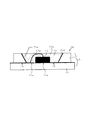
図1は、本発明によるLEDの第一の実施形態の構成を示している。
図1において、LED10は、シリコン基板11と、このシリコン基板11の凹陥部として形成されたホーン11a内にマウントされたLEDチップ12と、ホーン11a内に充填された樹脂材料から成る樹脂モールド13と、から構成されている。
FIG. 1 shows the configuration of a first embodiment of an LED according to the present invention.
In FIG. 1, an
上記シリコン基板11は、その表面が(100)面となるように平坦に形成されている。
そして、上記シリコン基板11は、表面から底面まで貫通しない厚さまでの凹陥部により形成されたホーン11aを備えている。
このホーン11aは、例えばTMAHによる液相の結晶異方性エッチングによって、その側面が(111)面となるように形成されている。
尚、上記ホーン11aの側面は、(111)面であることから、底面に対する傾斜角度が54.7度に選定されている。
この場合、ホーン11aは、エッチング工程の時間管理に基づいて、適宜の深さとなるように加工されており、ホーン11aの底面をできるだけシリコン基板11の底面に近づける、即ちホーン11aの底面におけるシリコン基板11の厚さをできるだけ薄くすることができ、これにより熱抵抗を低減することが可能である。
The
The
The
Since the side surface of the
In this case, the
そして、上記シリコン基板11は、図1にて、そのホーン11aの底面から左右の側面を介して表面にまで延びる一対の電極14及び15を備えている。
これらの電極14,15は、例えばホーン11aを形成したシリコン基板11の表面に金属薄膜を形成した後、この金属薄膜のパターンエッチングにより形成されるようになっている。
ここで、一方の電極14は、上記ホーン11aの底面の中央領域に配置されたチップ実装部14aを備え、またこの実装部14aのパターンは取り付けられるLEDチップ12の端子部と同一形状もしくは外形線の一部に同一形状を含む形状とし浮遊するLEDチップ12を溶融しているハンダの表面張力でパターンと端子とが一致するように移動させるセルフアライメントが行なわれ得るものとし、他方の電極15は、上記ホーン11aの底面にて、このチップ実装部14aに隣接する接続部15aを備えている。
In FIG. 1, the
These
Here, one
さらに、この場合、双方の電極14,15は、少なくとも側面の領域にて、その表面がミラー面として形成されている。尚、双方の電極14は、少なくとも側面の領域にて、その表面に別体のミラー面を備えるようにしてもよい。
Furthermore, in this case, the surfaces of both the
上記LEDチップ12は、公知の構成の例えば青色光を発生するLEDチップであって、その上面及び下面に図示しない電極部を備えており、上記シリコン基板11のホーン11a内の底面にマウントされ、上記一方の電極14のチップ実装部14a上にダイボンディングされることにより、下面の電極部がチップ実装部14aに電気的に接続されると共に、その上面の電極部が金線等のボンディングワイヤ12aにより、他方の電極15の接続部15aに電気的に接続されるようになっている。
The
上記樹脂モールド13は、エポキシ樹脂等の透光性樹脂材料から構成されており、この透光性樹脂材料に、粒状の蛍光体13aが混入されている。
従って、樹脂モールド13は、上記シリコン基板11のホーン11a内に充填され、硬化された後、内部に粒状の蛍光体13aが分散することになる。
ここで、上記粒状の蛍光体13aは、LEDチップ12の発光色に対応して例えば黄色の励起光を発生する蛍光体である。これにより、LEDチップ12からの青色光に励起されて、蛍光体13aが黄色の励起光を発生させ、この黄色の励起光がLEDチップ12からの青色光と混色されて、外部に白色光が出射するようになっている。
The
Therefore, after the
Here, the granular phosphor 13 a is a phosphor that generates, for example, yellow excitation light corresponding to the emission color of the
本発明実施形態によるLED10は、以上のように構成されており、製造の際には、本発明による製造方法に基づいて、以下のようにして製造される。
即ち、まず、平坦なシリコン基板11の(100)面である表面に対して、液相の結晶異方性エッチングによりホーン11aが形成される。この場合、エッチング剤としては、例えばTMAH(テトラメチル水酸化アンモニウム)が使用される。
このTMAHは、エッチングによるアンダーカットが比較的大きく、寸法制御が困難であるが、マスクのダメージが少なく、酸化膜マスクが使用可能であると共に、CMOSとの整合性が良好であるという利点を有している。これに対して、例えばKOHをエッチング剤として使用すると、アンダーカットは小さいが、CMOSとの整合性が悪い。
尚、このようなエッチングにより形成されるホーン11aは、その側面が(111)面として、傾斜角54.7度の斜面となる。
そして、エッチング時間を適宜に管理することによって、所望の深さのホーン11aが形成され得ることになる。
次工程の電極を形成する前に、例えばスパッタ法、CVD法、熱酸化法等で、Si表面を薄いSiO2層やSi3N4層で覆い、絶縁化する。
The
That is, first, the
This TMAH has a relatively large undercut due to etching and dimensional control is difficult, but has the advantages that the mask damage is small, an oxide film mask can be used, and the compatibility with CMOS is good. is doing. On the other hand, when KOH is used as an etchant, for example, the undercut is small, but the compatibility with the CMOS is poor.
Note that the
And the
Before forming the electrode for the next step, the Si surface is covered with a thin SiO2 layer or Si3N4 layer, for example, by sputtering, CVD, thermal oxidation, or the like, and insulated.
次に、ホーン11aを形成したシリコン基板11の表面全体に亘って、電極となるべき金属薄膜を形成した後、この金属薄膜をパターンエッチングすることにより、電極14,15を形成する。なお、パターンエッチングは電着レジスト、スプレーレジスト等の、立体形状に対して均一なレジスト膜を形成する手法を用いることが好適である。このとき、電極14,15の表面は、例えばアルミニウム,銀等の反射率の高い材料から成る薄膜をスパッタ,蒸着等により形成することによって、ミラー面として形成される。
続いて、一方の電極14のチップ実装部14aに対して、LEDチップ12をマウントし、ダイボンディングすると共に、LEDチップ12の表面の電極部をボンディングワイヤ12aにより他方の電極15の接続部15aに対してワイヤボンディングする。
Next, after forming a metal thin film to be an electrode over the entire surface of the
Subsequently, the
その後、ホーン11a内に、粒状の蛍光体13aを混入した樹脂材料を充填し、硬化させる。これにより、ホーン11a内に樹脂モールド13が形成される。以上で、本LED10が完成する。
Thereafter, the resin material mixed with the granular phosphor 13a is filled in the
このようにして製造されたLED10によれば、LEDチップ12に対して外部から電極14,15を介して給電することにより、LEDチップ12が駆動される。
そして、LEDチップ12から出射する光Lが、直接に、あるいはシリコン基板11のホーン11aの底面または側面で電極14,15のミラー面として形成された表面で高い反射率で反射されて、樹脂モールド13内の蛍光体13aに当たって、蛍光体13aを励起する。これにより、蛍光体13aから励起光が発生して、LEDチップ12からの青色光と混色され、白色光として、樹脂モールド13を介して上方に出射する。
According to the
Then, the light L emitted from the
この場合、LEDチップ12が例えば150W/m・kと高い熱伝導率を有するシリコン基板11上にマウントされるので、駆動時にLEDチップ12から発生する熱が効率良くシリコン基板11を介して放熱されることになる。
従って、LEDチップ12の温度上昇が抑制されることになり、LEDチップ12の発光効率が熱によって低下せず、これによりLEDチップの発熱によって出射光束が減少したり、寿命が低下するようなことはない。
また、LEDチップ12に対する電気的接続のための電極14,15がパターニングによって形成されるので、マルチチップ化した場合に、各LEDチップ12を互いに直列接続することが可能であり、Vfの低いLEDチップ12に電流が集中するようなこともない。
さらに、上記ホーン11aの側面が(111)面から構成されていることによって、このホーン11aの側面が、通常の加工、例えば金属材料の切削加工,ポンチ加工や樹脂成形では得られないような優れたミラー面として形成されることになる。
In this case, since the
Therefore, the temperature rise of the
In addition, since the
Further, since the side surface of the
さらに、比較的安価で入手可能なシリコン基板11上に、既存の半導体製造工程により、他のIC等の半導体デバイスを一体に構成することが可能である。従って、例えばLEDチップ12の点灯や点滅を行なうための駆動回路を組み込むことも可能となり、駆動回路を含めて、小型に構成され得ることになる。
Further, it is possible to integrally form other semiconductor devices such as ICs on the
このようにして、上記LED10によれば、シリコン基板11を使用することにより、LEDチップ12の発熱が効率良く放熱されると共に、パターニングにより形成される電極14,15により、容易にマルチチップ化して、各LEDチップ12を互いに直列接続することが可能であるので、バラツキによるVfの低いLEDチップ12への電流集中が回避され得ることになる。
また、上記LED10は、既設の半導体製造装置を利用して容易に製造され得るので、特別の設備投資も必要なく、比較的低コストで製造され得ることになる。
In this way, according to the
Moreover, since the
図2は、本発明によるLEDの第二の実施形態の構成を示している。
図2において、LED20は、図1に示したLED10とほぼ同様の構成であるので、同じ構成要素には同じ符号を付して、その説明を省略する。
即ち、LED20は、シリコン基板21と、このシリコン基板21の凹陥部として形成されたホーン21a内にマウントされたLEDチップ12と、ホーン21a内に充填された樹脂材料から成る樹脂モールド13と、から構成されている。
FIG. 2 shows the configuration of a second embodiment of an LED according to the present invention.
2, the
That is, the
ここで、上記シリコン基板21は、二層に積層されて構成されている。
即ち、上記シリコン基板21は、下方の第一の基板22と、上方の第二の基板23と、から構成されている。
上記第一の基板22は、平坦なシリコン基板から構成されており、その表面に金属薄膜のパターニングによって、電極14,15が形成されている。この場合、電極14,15は、第一の基板22の表面に沿って、即ちシリコン基板21の内部を通って側方まで延びている。
これに対して、第二の基板23は、その表面が(100)面となるように平坦に形成されており、上下に貫通するように形成されたホーン21aを備えている。
このホーン21aは、前述したLED10におけるホーン11aと同様に、例えばTMAHによる液相の結晶異方性エッチングによって、その側面が(111)面となるように形成されており、その側面全体がミラー面を備えている。このミラー面は、公知の如く、ホーン11aの表面に対して反射率の高い材料の薄膜を蒸着,メッキ等により形成することにより、得られる。
Here, the
That is, the
The
On the other hand, the 2nd board |
Like the
このような構成のLED20は、製造の際には、本発明による製造方法に基づいて、以下のようにして製造される。
即ち、まず、第一の基板22となるシリコン基板の表面に金属薄膜のパターンエッチングによって、電極14,15を形成する。
これと並行して、第二の基板23となるシリコン基板の(100)面である表面に対して、液相の結晶異方性エッチングによりホーン21aが形成される。この場合、ホーン21aが第二の基板23を上下に貫通していることから、ホーン21aの深さをあまり高精度に設定する必要がないことから、エッチング工程の時間管理が容易になる。
The
That is, first, the
In parallel with this, the horn 21a is formed on the surface which is the (100) plane of the silicon substrate to be the
次に、第二の基板23のホーン21aの側面に対して、ミラー面を蒸着,メッキ等により形成した後、第二の基板23を第一の基板22上に貼り合わせる。
続いて、上記ホーン21aの底面に露出している一方の電極14のチップ実装部14aに対して、LEDチップ12をマウントし、ダイボンディングすると共に、LEDチップ12の表面の電極部をボンディングワイヤ12aにより他方の電極15の接続部15aに対してワイヤボンディングする。
Next, a mirror surface is formed on the side surface of the horn 21 a of the
Subsequently, the
その後、ホーン21a内に、粒状の蛍光体13aを混入した樹脂材料を充填し、硬化させる。これにより、ホーン21a内に樹脂モールド13が形成される。 尚、電極を形成する前に、例えばスパッタ法、CVD法、熱酸化法等で、Si表面を薄いSiO2層やSi3N4層で覆い、絶縁化する。
以上で、本LED20が完成する。
Thereafter, the resin material mixed with the granular phosphor 13a is filled in the horn 21a and cured. Thereby, the
This completes the
このようにして製造されたLED20によれば、図1に示したLED10と同様に作用すると共に、シリコン基板21が二層に構成されていることにより、第一の基板22の表面に複雑な配線パターンを形成することが可能となり、また第二の基板23のホーン21aの内面全体に亘ってミラー面が形成されるので、外部への光の取出し効率が向上することになる。
According to the
図3は、本発明によるLEDの第三の実施形態の構成を示している。
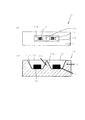
図3において、LED30は、図2に示したLED20と同様の構成であるので、同じ構成要素には同じ符号を付して、その説明を省略する。
上記LED30は、第一の基板22の上面中央付近にて、電極14,15が互いに間隔をあけて突き合わせられたチップ実装部14b,15bを備えるように形成されている。
そして、これらのチップ実装部14b,15bの上に、所謂フリップチップタイプのLEDチップ31が、その下面の両側縁に設けられた電極部を載置するように、マウントされ、電気的に接続されるようになっている。
このような構成のLED30によれば、図2に示したLED20と同様に作用することになる。
FIG. 3 shows the configuration of a third embodiment of an LED according to the present invention.
In FIG. 3, the
The
A so-called flip chip
According to the
図4は、本発明によるLEDの第四の実施形態の構成を示している。
図4において、LED40は、例えば図1によるLED10に対して、シリコン基板11上にて、ホーン11aに隣接して、アクチュエータとして熱電バイモルフアクチュエータ41が構成されている。
この熱電バイモルフアクチュエータ41は、それ自体公知の構成であって、シリコン基板11上に半導体製造工程にて所謂MEMS技術を利用して、エッチングにより構成されるものである。
そして、上記熱電バイモルフアクチュエータ41は、図示しない電極を介して通電されることにより、図5に示すように、半導体基板11上にて変位して、ホーン11aの上面の一部を覆うようになっている。
FIG. 4 shows the configuration of a fourth embodiment of an LED according to the present invention.
In FIG. 4, the
The thermoelectric bimorph actuator 41 has a publicly known configuration, and is formed on the
When the thermoelectric bimorph actuator 41 is energized through an electrode (not shown), the thermoelectric bimorph actuator 41 is displaced on the
このような構成のLED40によれば、シリコン基板11のホーン11aからは、前述したLED10の場合と同様にして、光が外部に出射すると共に、上記熱電バイモルフアクチュエータ41の動作時には、ホーン11aの上端の開口部による発光部全体から外部に光が出射することになると共に、上記熱電バイモルフアクチュエータ41の非動作時には、上記発光部の一部が上記熱電バイモルフアクチュエータ41によって遮光されることになり、発光部の形状を変更することが可能である。従って、例えば上記LED40を自動車の前照灯の光源として使用するような場合に、走行ビームとすれ違いビームの切換えが可能になる。
尚、このようなホーン11aの上端の開口部による発光部の形状変更は、シリコン基板11上に構成され得る他の型式のアクチュエータによっても実現することができる。
According to the
The shape change of the light emitting portion by the opening at the upper end of the
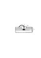
図6は、本発明によるLEDの第五の実施形態の構成を示している。
図6において、LED50は、例えば図1によるLED10に対して、シリコン基板11上にて、ホーン11aに隣接して、アクチュエータとして垂直櫛歯型静電アクチュエータ51が構成されている。
この垂直櫛歯型静電アクチュエータ51は、それ自体「Vertical Comb」として公知の構成であって、シリコン基板11上に半導体製造工程にて所謂MEMS技術を利用して、エッチングにより構成されるものである。
そして、上記垂直櫛歯型静電アクチュエータ51は、図示しない電極を介して通電されることにより、図6にて矢印Aで示すように、半導体基板11上にて揺動して、ホーン11aの上面から出射する光束の一部を遮断するようになっている。
FIG. 6 shows the configuration of a fifth embodiment of an LED according to the present invention.
In FIG. 6, the
The vertical comb-shaped electrostatic actuator 51 has a configuration known as “Vertical Comb” itself, and is configured by etching on a
When the vertical comb electrostatic actuator 51 is energized through an electrode (not shown), it swings on the
このような構成のLED50によれば、シリコン基板11のホーン11aからは、前述したLED10の場合と同様にして、光が外部に出射すると共に、上記垂直櫛歯型静電アクチュエータ51の揺動によって、ホーン11aの上端の開口部による発光部全体から出射する光の一部が、選択的に遮断されることにより、配光パターンが変更される。従って、例えば上記LED40を自動車の前照灯の光源として使用するような場合に、所謂AFS機能を実現することができる。
尚、このようなホーン11aの上端の開口部による発光部の形状変更は、シリコン基板11上に構成され得る他の型式のアクチュエータによっても実現することができる。
According to the
The shape change of the light emitting portion by the opening at the upper end of the
図7は、本発明によるLEDの第六の実施形態の構成を示している。
図7において、LED60は、図1に示したLED10とほぼ同様の構成であるので、同じ構成要素には同じ符号を付して、その説明を省略する。
即ち、LED60は、シリコン基板11と、このシリコン基板11の凹陥部として並んで形成された二つのホーン11a,11b内にそれぞれマウントされた二つのLEDチップ12と、ホーン11a,11b内にそれぞれ充填された樹脂材料から成る樹脂モールド13と、から構成されている。
FIG. 7 shows the configuration of a sixth embodiment of an LED according to the present invention.
In FIG. 7, the
That is, the
ここで、上記シリコン基板11は、その表面が(100)面となるように平坦に形成されており、表面から中間高さまでの凹陥部により形成された二つのホーン11a,11bを備えている。
これらのホーン11a,11bは、前述したLED10におけるホーン11aと同様に、例えばTMAHによる液相の結晶異方性エッチングによって、その側面が(111)面となるように形成されている。
Here, the
These
さらに、上記ホーン11a,11bは、互いに離れて配置されており、これらの間に仕切り壁11cを画成している。
この仕切り壁11cは、シリコン基板11の上面と同じ高さを有していると共に、その上面が平坦に形成されている。尚、この上面の幅は、例えば数μm乃至数10μm程度に選定される。
尚、この仕切り壁11cは、図8に示すように、上端が稜線を有するように尖って形成されていてもよい。これにより、仕切り壁11cの高さを変えることなく、各LEDチップ12の間隔を小さくすることができる。
Further, the
The
In addition, as shown in FIG. 8, this
そして、上記シリコン基板11は、図1にて、そのホーン11a,11bの仕切り壁11cの側面を含む底面及び側面に、反射ミラーを兼ねる電極(図示せず)を備えており、この電極は、双方のLEDチップ12を直列にまたは並列に接続して、これらのLEDチップ12に対して給電を行なうようになっている。
これらの電極は、例えばホーン11aを形成したシリコン基板11の表面に例えば銀等の金属薄膜を形成した後、この金属薄膜のパターンエッチングにより形成されるようになっている。
The
These electrodes are formed, for example, by forming a metal thin film such as silver on the surface of the
さらに、これらの電極は、ホーン11a,11bの側面から上記シリコン基板11の上面にまで延びており、この上面領域がボンディングワイヤ,リード線を利用して、あるいはハンダ付け,銀ペースト等を利用して、実装基板上の接続部に対して電気的に接続され得るようになっている。
Further, these electrodes extend from the side surfaces of the
このような構成のLED60は、製造の際には、本発明による製造方法に基づいて、図9を参照して、以下のようにして製造される。
即ち、まず、(100)面の表面が光学研磨処理により平坦化されている厚さ525μmの単結晶シリコンウェハを使用し、図9(A)に示すように、シリコン基板11の表面に拡散炉により厚さ500nmの熱酸化シリコン膜11dが形成される。
そして、図9(B)に示すように、平坦なシリコン基板11の表面に対して、フォトリソグラフィ法によりレジストパターンが形成された後、バッファードフッ酸(BHF)により熱酸化シリコン膜11dがエッチング除去され、熱酸化シリコン膜11dのパターンが形成される。
The
That is, first, a 525 μm-thick single crystal silicon wafer having a (100) surface planarized by optical polishing is used, and a diffusion furnace is formed on the surface of the
Then, as shown in FIG. 9B, a resist pattern is formed on the surface of the
その後、図9(C)に示すように、例えばTMAH溶液による液相の結晶異方性エッチングによって、ホーン11a,11bが同時に形成された後、BHF溶液により、すべての残っている熱酸化シリコン膜11dが除去される。
次に、図9(D)に示すように、再び拡散炉によってホーン11a,11bを含むシリコン基板11の表面全体に、厚さ500nmの熱酸化シリコン膜11eが形成され、基板全体が絶縁化された後、スパッタ法により、電極膜11fが成膜される。この電極膜11fは、例えば順次に成膜された厚さ20nmのTi及び厚さ200nmのCuから構成されている。
Thereafter, as shown in FIG. 9C, after the
Next, as shown in FIG. 9D, a thermal
続いて、図9(E)に示すように、電着レジストまたはスプレーレジストコーティングによって、ホーン11a,11bを含んだシリコン基板11の表面全体に、レジスト11gが塗布され、フォトリソグラフィ法によりレジストのパターンニングが行なわれる。
その後、図9(F)に示すように、上記レジストパターン11gをマスクとして、上記電極膜11fがウェットエッチングされ、電極パターン11hが形成される。尚、この場合、電極パターン11hは、双方のLEDチップ12を直列に接続するように、形成されている。
Subsequently, as shown in FIG. 9E, a resist 11g is applied to the entire surface of the
Thereafter, as shown in FIG. 9F, the electrode film 11f is wet etched using the resist
次に、図9(G)に示すように、電解メッキ法により順次に厚さ5μmのNi及び厚さ3μmのAgから成る反射ミラー膜11iが形成される。
続いて、図9(H)に示すように、各ホーン11a,11bの底部に形成された一方の電極を構成する電極膜パターン11f上に対して、LEDチップ12をマウントし、ハンダまたは共晶接合によってダイボンディングすると共に、LEDチップ12の表面の電極部をボンディングワイヤ12aにより他方の電極を構成する電極膜パターン11fに対してワイヤボンディングする。
その後、ホーン11a,11b内に、粒状の蛍光体13aを混入した樹脂材料を充填し、硬化させる。これにより、ホーン11a内に樹脂モールド13が形成される。以上で、本LED60が完成する。
Next, as shown in FIG. 9G, a reflective mirror film 11i made of Ni having a thickness of 5 μm and Ag having a thickness of 3 μm is sequentially formed by electrolytic plating.
Subsequently, as shown in FIG. 9H, the
Thereafter, the
このようにして製造されたLED60によれば、図1に示したLED10と同様に作用すると共に、二つのLEDチップ12が仕切り壁11cを介して配置されているので、LEDチップ12間の光吸収が抑制されることになり、出力光の損失が低減することになる。
例えば単独で3V,350mAのバイアス印加によって120mWの光出力が得られるLEDチップ12を二個使用して、6V,350mAのバイアスを印加したところ、二倍の240mWの光出力が得られた。これは、仕切り壁11cの作用によって、LEDチップ12間の光吸収が抑制されたことによるものと推察される。
According to the
For example, when two
図10は、本発明によるLEDの第七の実施形態の構成を示している。
図10において、LED70は、図7に示したLED60とほぼ同様の構成であるので、同じ構成要素には同じ符号を付して、その説明を省略する。
即ち、LED70は、シリコン基板11と、このシリコン基板11の凹陥部として並んで形成された二つのホーン11a,11b内にそれぞれマウントされた二つのLEDチップ12と、ホーン11a,11b内にそれぞれ充填された樹脂材料から成る樹脂モールド13と、から構成されている。
この場合、仕切り壁11cは、その高さがシリコン基板11の上面より低い稜線を構成している点でのみ、図7に示したLED60とは異なる構成になっている。
FIG. 10 shows a configuration of a seventh embodiment of the LED according to the present invention.
In FIG. 10, the
That is, the
In this case, the
このような構成のLED70は、製造の際には、本発明による製造方法に基づいて、図11を参照して、以下のようにして製造される。
即ち、まず図11(A)に示すように、シリコン基板11の表面に拡散炉により厚さ500nmの熱酸化シリコン膜11dが形成される。
そして、図11(B)に示すように、平坦なシリコン基板11の表面に対して、フォトリソグラフィ法によりレジストパターンが形成された後、BHF溶液により熱酸化シリコン膜11dがエッチング除去され、熱酸化シリコン膜11dのパターンが形成される。
The
That is, first, as shown in FIG. 11A, a thermal
Then, as shown in FIG. 11B, after a resist pattern is formed on the surface of the
その後、図11(C)に示すように、プラズマCVD法により厚さ200nmの窒化シリコン膜11jがシリコン基板11の表面全体に成膜される。
続いて、図11(D)に示すように、フォトリソグラフィ法により形成されたレジストマスク(図示せず)を使用して、熱リン酸処理またはプラズマエッチング処理により、上記窒化シリコン膜11jがパターニングされる。
次に、図11(E)に示すように、例えばTMAH溶液による異方性エッチングによって、浅いホーン11a,11bが同時に形成された後、図11(F)に示すように、洗浄してから熱リン酸処理またはプラズマエッチング処理によって、すべての残っている窒化シリコン膜11jが除去された後、再びTMAH溶液による液相の結晶異方性エッチングにより、仕切り壁11cにより分離されたホーン11a,11bを含む一つの大きなホーンが形成されることになる。
その後、熱酸化シリコン膜11dが除去された後、図11(G)に示すように、再び拡散炉によってホーン11a,11bを含むシリコン基板11の表面全体に、厚さ500nmの熱酸化シリコン膜11eが形成され、基板全体が絶縁化される。
Thereafter, as shown in FIG. 11C, a silicon nitride film 11j having a thickness of 200 nm is formed on the entire surface of the
Subsequently, as shown in FIG. 11D, the silicon nitride film 11j is patterned by thermal phosphoric acid treatment or plasma etching treatment using a resist mask (not shown) formed by photolithography. The
Next, as shown in FIG. 11 (E), after
Thereafter, after the
その後は、図9(D)〜(H)と同様にして、スパッタ法により、電極膜11fが成膜され、パターンエッチングにより電極パターン11hが形成され、電極パターン11hの表面に、反射ミラー膜11iが形成された後、ホーン11a,11b内の電極パターン11h上にLEDチップ12がダイボンディングされ、隣接する電極パターン11hに対してワイヤボンディングされ、さらにホーン11a,11b内に、粒状の蛍光体13aを混入した樹脂材料が充填され、硬化されることにより、ホーン11a内に樹脂モールド13が形成される。
以上で、本LED70が完成する。
Thereafter, in the same manner as in FIGS. 9D to 9H, the electrode film 11f is formed by sputtering, the
Thus, the
このような構成のLED70によれば、図1に示したLED10と同様に作用すると共に、二つのLEDチップ12が比較的低い仕切り壁11cを介して配置されているので、LEDチップ12間の光吸収が抑制されることになり、出力光の損失が低減することになる。
このLED70について、前記LED60と同様に発光特性の評価を行なったところ、同様に二倍の光出力が得られると共に、各LEDチップ12の間隔が短縮されたことにより、点光源に近い発光特性が得られた。
According to the
When the light emission characteristics of the
尚、上述したLED70においては、仕切り壁11cは、側面がホーン11a,11bと同じ傾斜角を有する平坦な傾斜面として構成されているが、これに限らず、図12に示すように、シリコン基板11を、LED20の場合と同様の二層構造にして、下方の第一の基板22上に仕切り壁11cを形成すると共に、第二の基板23に一つの大きなホーン71を形成するようにしてもよい。この場合、ホーン71と仕切り壁11cは、別々に液相の結晶異方性エッチングにより形成されるので、エッチングを適宜に制御することにより、互いに異なる傾斜角に形成することも可能である。
In addition, in LED70 mentioned above, although the
また、上述したLED60及び70において、仕切り壁11cは、側面が平坦な傾斜面として構成されているが、これに限らず、仕切り壁11cを形成する際の異方性エッチングの条件を変更したり、あるいは途中で異方性エッチングから等方性エッチングに変更する等によって、図13(A)に示すように、仕切り壁11cの側面を凹状に、あるいは図13(B)に示すように、仕切り壁11cの側面を凸状に、それぞれ形成するようにしてもよい。
尚、図13(B)の場合、エッチングの制御によって、仕切り壁11cの高さを適宜に設定することも可能である。
このような仕切り壁11cの各種形状によって、LEDチップ12から出射した光の仕切り壁11cの側面による反射を制御することが可能であり、この反射の制御によって、所望の輝度分布や配光特性を実現することが可能である。
Moreover, in LED60 and 70 mentioned above, although the
In the case of FIG. 13B, the height of the
By such various shapes of the
このようにして、上述したLED60,70によれば、LEDチップ12の間に、仕切り壁11cを設けることによって、LEDチップ12間の光吸収を抑制することができるので、光出力を増大させることができる。
また、仕切り壁11cの形状に基づいて、LEDチップ12の間隔を適宜に設定することができるので、特にシリコン基板11の上面より低い仕切り壁11cの場合には、LEDチップ12の間隔がより一層小さくされ得るので、実質的に点光源と同様の配光特性が得られると共に、各LEDチップ12からの光の混色を行なわせる場合には、各LEDチップ12からの光の光束のミキシング効果が高められることになる。
また、上記LED60,70においては、二個のLEDチップ12が搭載されているが、これに限らず、三個以上のLEDチップが搭載されていてもよく、特に光の三原色である例えば赤,緑,青のLEDチップが搭載されている場合、各LEDチップからの光の光束のミキシング効果が高められることによって、演色性の良好な白色光が得られることになる。
In this way, according to the
Moreover, since the space | interval of the
In the
図14は、本発明によるLEDの第八の実施形態の構成を示している。
図14において、LED80は、図1に示したLED10とほぼ同様の構成であるので、同じ構成要素には同じ符号を付して、その説明を省略する。
即ち、LED80は、シリコン基板81と、このシリコン基板81の凹陥部として形成されたホーン81a内にマウントされたLEDチップ12と、ホーン81a内に充填された樹脂材料から成る樹脂モールド13と、から構成されている。
FIG. 14 shows the configuration of an eighth embodiment of an LED according to the present invention.
In FIG. 14, the
That is, the
ここで、上記シリコン基板81は、その表面が(100)面となるように平坦に形成されており、表面から中間高さまでの凹陥部により形成されたホーン81aを備えていると共に、このホーン81aに隣接して、即ち図14(A)の断面図にてホーン81aの両側に隣接して形成された二つのコンタクトホール81b,81cを備えている。
これらのコンタクトホール81b,81cは、ホーン81aと同様に、例えばTMAHによる液相の結晶異方性エッチングによって、その側面が(111)面となるように形成されている。
Here, the
Similar to the
そして、上記シリコン基板81は、図14(A)にて、そのホーン81aの底面から左右の側面を介してシリコン基板81の表面に、そしてそれぞれ左右のコンタクトホール81b,81cを介して端縁まで延びる一対の電極82,83を備えている。
これらの電極82,83は、例えばホーン81a及びコンタクトホール81b,81cを形成したシリコン基板81の表面に金属薄膜を形成した後、この金属薄膜のパターンエッチングにより形成されるようになっている。
ここで、一方の電極82は、上記ホーン81aの底面の中央領域に配置されたチップ実装部82aを備えており、他方の電極83は、上記ホーン81aの底面にて、このチップ実装部82aに隣接する接続部83aを備えている。
Then, in FIG. 14A, the
These
Here, one
さらに、この場合、双方の電極82,83は、少なくともホーン81aの側面の領域にて、その表面がミラー面として形成されている。尚、双方の電極82,83は、少なくとも側面の領域にて、その表面に別体のミラー面を備えるようにしてもよい。
Furthermore, in this case, the surfaces of both
また、上記コンタクトホール81b,81cは、それぞれシリコン基板81の下面にまで達しており、コンタクトホール81b,81c内にも形成された電極82,83の一部が、コンタクトホール81b,81cの下縁から下方に露出するようになっている。
The contact holes 81b and 81c reach the lower surface of the
このような構成のLED80は、製造の際には、本発明による製造方法に基づいて、図15を参照して、以下のように製造される。
即ち、まず(100)面の表面が光学研磨処理により平坦化されている厚さ525μmの単結晶シリコンウェハを使用し、図15(A)に示すように、シリコン基板81の表面に拡散炉により厚さ500nmの熱酸化シリコン膜81dが形成される。
そして、図15(B)に示すように、平坦なシリコン基板81の表面に対して、フォトリソグラフィ法によりレジストパターンが形成された後、BHF溶液により熱酸化シリコン膜11dがエッチング除去され、熱酸化シリコン膜11dのパターン(コンタクトホール形成用)が形成される。
The
That is, first, a 525 μm-thick single crystal silicon wafer having a (100) surface planarized by an optical polishing process is used, and a surface of a
Then, as shown in FIG. 15B, a resist pattern is formed on the surface of the
その後、図15(C)に示すように、85℃に加熱したTMAH溶液による液相の結晶異方性エッチングによって、(111)面から成る斜面により包囲された浅い凹陥部81e,81fが形成された後、シリコン基板81が一旦TMAH溶液から引き上げられ、図15(D)に示すように、再びフォトリソグラフィ法によるレジストパターンを使用して、熱酸化シリコン膜11dのパターン(ホーン形成用)が形成される。
次に、図15(E)に示すように、再びTMAH溶液による異方性エッチングによって、ホーン81a及びコンタクトホール81b,81cが形成された後、シリコン基板81がTMAH溶液から引き上げられる。
続いて、図15(F)に示すように、BHF溶液により、すべての残っている熱酸化シリコン膜81dが除去され、再び拡散炉によってシリコン基板81の表面全体に、厚さ500nmの熱酸化シリコン膜81gが形成され、基板表面が絶縁化される。
Thereafter, as shown in FIG. 15C,
Next, as shown in FIG. 15E, after the
Subsequently, as shown in FIG. 15F, all the remaining thermal silicon oxide film 81d is removed by the BHF solution, and the thermal oxide silicon having a thickness of 500 nm is again formed on the entire surface of the
次に、図15(G)に示すように、スパッタ法により順次に成膜された例えばTi及びCuから成る電極層そして反射膜81h’が成膜される。
その後、電着レジストまたはスプレーレジストコーティングによって、シリコン基板81の表面全体に、レジストが塗布され、フォトリソグラフィ法によりレジストのパターンニングが行なわれ、このレジストパターンをマスクとして、上記電極層及び反射膜がウェットエッチングされ、図15(H)に示すように、電極パターン81h(電極82,83)が形成される。この後、例えば電気メッキ等によりNi2μm、Ag3μmの膜を形成し、電極/反射膜を形成することができる。
Next, as shown in FIG. 15G, an electrode layer made of, for example, Ti and Cu and a
Thereafter, a resist is applied to the entire surface of the
次に、図15(I)に示すように、ホーン81aの底部に形成された一方の電極を構成する電極パターン81h上に対して、LEDチップ12をマウントし、ハンダリフロー法,共晶接合,銀ペースト等によってダイボンディングすると共に、LEDチップ12の表面の電極部をボンディングワイヤ12aにより他方の電極を構成する電極パターン81hに対してワイヤボンディングする。
その後、ホーン81a内に、粒状の蛍光体13aを混入した樹脂材料を充填し、硬化させる。これにより、図15(J)に示すように、ホーン81a内に樹脂モールド13が形成される。
以上で、本LED80が完成する。
Next, as shown in FIG. 15 (I), the
Thereafter, the resin material mixed with the granular phosphor 13a is filled in the
Thus, the
そして、上記LED80を実装基板84に実装する場合には、図15(K)に示すように、LED80のパッケージを、実装基板84上の所定位置に載置し、ハンダリフローにより、コンタクトホール81b,81cの下縁に延びる電極82,83を、実装基板84上の導電パターンから成る接続部84a,84bに対して接続する。
これにより、LED90の実装が完了する。
When the
Thereby, the mounting of the
このような構成のLED80によれば、図1に示したLED10と同様に作用すると共に、実装基板84への実装の際に、コンタクトホール81b,81cの下縁に延びる電極82,83が、直接に上記実装基板84上の接続部84a,84bと接触し、ハンダ付け等により接続され得るので、ボンディングワイヤやリード線等が不要になると共に、他の部品を隣接して実装することが可能である。 このLED80について、前記LED60と同様に、3V,350mAのバイアスを印加して、発光特性の評価を行なったところ、110mWの白色光が得られた。
According to the
図16は、本発明によるLEDの第九の実施形態の構成を示している。
図16において、LED90は、図14に示したLED80とほぼ同様の構成であるので、同じ構成要素には同じ符号を付して、その説明を省略する。
即ち、LED90は、コンタクトホール81b,81cの代わりに、シリコン基板81の両端縁にコンタクトエッジ81i,81jを備えている点でのみ異なる構成になっている。
ここで、上記コンタクトエッジ81i,81jは、それぞれシリコン基板81の両端縁にて、ちょうど前記コンタクトホール81b,81cを中心で半分に分割した形状を有している。
これらのコンタクトエッジ81i,81jは、ホーン81aと同様に、例えばTMAHによる液相の結晶異方性エッチングによって、その側面が(111)面となるように形成されている。
FIG. 16 shows the configuration of a ninth embodiment of an LED according to the present invention.
In FIG. 16, the
That is, the
Here, the contact edges 81i and 81j have a shape obtained by dividing the contact holes 81b and 81c in half at the center at both ends of the
Similar to the
そして、上記シリコン基板81の表面に形成された電極82,83は、図16(A)にて、そのホーン81aの底面から左右の側面を介してシリコン基板81の表面に、そしてそれぞれ左右のコンタクトエッジ81i,81j内の下縁まで延びるようになっている。
The
このような構成のLED80は、製造の際には、本発明による製造方法に基づいて、図17を参照して、以下のように製造される。
即ち、図14に示したLED70の場合と同様に、図15(A)〜(H)に示すように、シリコン基板81の表面にホーン81a及びコンタクトホール81b,81cが形成されると共に、電極パターン81hが形成される。
その際、電極パターン81h(電極82,83)は、ホーン81aからシリコン基板81の上面を介して、各コンタクトホール81b,81c内にて、その下縁まで延びるようになっている。
The
That is, as in the case of the
At this time, the
そして、図17(A)に示すように、シリコン基板81は、それぞれコンタクトホール81b,81cの中心を通るように、ダイシングによって、上下に切断される。これにより、各コンタクトホール81b,81cは、それぞれ半分に分割されて、コンタクトエッジ81i,81jとなる。
その後、図17(B)に示すように、ホーン81aの底部に形成された一方の電極82を構成する電極パターン81h上に対して、LEDチップ12をマウントし、ハンダリフロー法,共晶接合,銀ペースト等によってダイボンディングすると共に、LEDチップ12の表面の電極部をボンディングワイヤ12aにより他方の電極83を構成する電極パターン81hに対してワイヤボンディングする。
その後、ホーン81a内に、粒状の蛍光体13aを混入した樹脂材料を充填し、硬化させる。これにより、図17(C)に示すように、ホーン81a内に樹脂モールド13が形成される。
以上で、本LED90が完成する。
Then, as shown in FIG. 17A, the
Thereafter, as shown in FIG. 17B, the
Thereafter, the resin material mixed with the granular phosphor 13a is filled in the
Thus, the
そして、上記LED90を実装基板84に実装する場合には、図17(D)に示すように、LED90のパッケージを、実装基板84上の所定位置に載置し、ハンダリフローにより、コンタクトエッジ81i,81jの下縁に延びる電極82,83を、実装基板84上の導電パターンから成る接続部84a,84bに対して接続する。
これにより、LED90の実装が完了する。
この場合、コンタクトホールの代わりに、コンタクトエッジ81i,81jが設けられていることによって、実装の際に、コンタクトエッジ81i,81jに対するクリームハンダのポッティングが容易に行なわれ得ることになり、作業性が向上する。
When mounting the
Thereby, the mounting of the
In this case, since the contact edges 81i and 81j are provided instead of the contact holes, the cream solder can be easily potted with respect to the contact edges 81i and 81j at the time of mounting. improves.
図18は、本発明によるLEDの第十の実施形態の構成を示している。
図18において、LED100は、図14に示したLED80とほぼ同様の構成であるので、同じ構成要素には同じ符号を付して、その説明を省略する。
即ち、LED100は、シリコン基板81の下面のホーン81aに対応する領域に、金属薄膜101を備えている点でのみ異なる構成になっている。
ここで、上記金属薄膜101は、例えばAuまたはAgから構成されており、スパッタ法により成膜され、フォトリソグラフィ法及びウェットエッチングを用いてパターンニングされる。
FIG. 18 shows the configuration of a tenth embodiment of the LED according to the present invention.
In FIG. 18, the
That is, the
Here, the metal
そして、上記LED100を実装基板84に実装する場合には、図18に示すように、LED100のパッケージを、実装基板84上の所定位置に載置し、ハンダリフローにより、コンタクトホール81b,81cの下縁に延びる電極82,83を、実装基板84上の導電パターンから成る接続部84a,84bに対して接続する。
これにより、LED100の実装が完了する。
この場合、シリコン基板81の下面に備えられた金属薄膜101が、実装基板84上の放熱用導電パターン部84cに当接することによって、LEDチップ12から発生する熱が、シリコン基板81から金属薄膜101を介して、実装基板84の放熱用導電パターン部84cに伝達されることにより、LEDチップ12から発生する熱が効果的に放熱され得ることになる。
When the
Thereby, the mounting of the
In this case, the metal
図19は、本発明によるLEDの第十一の実施形態の構成を示している。
図19において、LED110は、図18によるLED100の変形例であって、シリコン基板81の下面の金属薄膜101が形成される領域にて、熱酸化シリコン膜81gが除去されている点でのみ異なる構成になっている。
FIG. 19 shows the configuration of an eleventh embodiment of an LED according to the present invention.
In FIG. 19, an
このような構成のLED110によれば、上記LED110をヒートシンク111に実装する場合には、図20に示すように、LED110のパッケージを、ヒートシンク111の表面に対して、熱伝導性シート112を介して載置すると共に、コンタクトホール81b,81cをリードフレーム113,114上に載置して、ハンドリフローにより、コンタクトホール81b,81cの下縁に延びる電極82,83を、それぞれリードフレーム113,114に対して接続する。
これにより、LED110の実装が完了する。
この場合、シリコン基板81の下面に備えられた金属薄膜101が、シリコン基板81の下面に直接に接触すると共に、熱伝導性シート112を介してヒートシンク111に接触することにより、LEDチップ12からの熱がシリコン基板81,熱伝導性シート112を介してヒートシンク111に対して伝達されることにより、例えば2℃/Wという非常に小さな熱抵抗となり、より一層放熱効果が向上することになる。
According to the
Thereby, the mounting of the
In this case, the metal
図21は、本発明によるLEDの第十二の実施形態の構成を示している。
図21において、図1に示したLEDと同じ構成要素には同じ符号を付して、その説明を省略する。
即ち、このLEDは、シリコン基板11と、シリコン基板11の凹陥部として形成されたホーン11aと、その中央にマウントされたLEDチップ12と、ホーン11a内に充填された樹脂材料からなる樹脂モールド13と、レンズ200から構成されている。
このレンズ200は、ホーン11aに樹脂モールド13を充填後、未硬化のうちに、ホーン上部に配置し、その後硬化することによって固定される。特に、ホーンに隣接してレンズ位置決め用の凹部201を形成することにより、レンズ取り付けの際に正確且つ簡易に取り付けることができ、好適である。この凹部201はホーン形成時の液相エッチングによって同時に形成することが可能であるため、事実上マスクの精度ををそのままレンズの位置決めに持ち込むことができる。
なお、図21においては凹部201は長方形のものを2箇所形成しているが、3箇所以上や、ホーンを囲むような略円形、略多角形であってもよい。また、図22にあるように、ホーンを2段階として、そのうちの上段を位置決め用の凹部として用いても同じ効果が得られる。
FIG. 21 shows the configuration of a twelfth embodiment of an LED according to the present invention.
In FIG. 21, the same components as those of the LED shown in FIG.
That is, this LED includes a
This
In FIG. 21, the
図23は、本発明によるLEDの第十三の実施形態の構成を示している。
図23において、図1に示したLEDと同じ構成要素には同じ符号を付して、その説明を省略する。
即ち、このLEDは、シリコン基板11と、シリコン基板11の凹陥部として形成されたホーン11aと、その中央にマウントされたLEDチップ12と、ホーン11a内に充填された樹脂材料からなる樹脂モールド13と、球形レンズ200から構成されている。
この球形レンズ200は、ホーン11aに樹脂モールド13を充填後、未硬化のうちに、ホーン上部に配置し、その後硬化することによって固定される。特に、ホーンの形状を正方形とすれば、固定の際には球形レンズ200をホーンの縁に押し付けるように固定することで、レンズの位置を一義的に決めることが可能であり、光軸のずれが起きにくいという利点を有する。レンズ自体の材質はガラスや樹脂材料など、光透過性材料であれば良いが、モールド樹脂によって接着、固定されるため、当該樹脂と密着性の良いものであればより好適である。
FIG. 23 shows the configuration of a thirteenth embodiment of an LED according to the present invention.
In FIG. 23, the same components as those of the LED shown in FIG.
That is, this LED includes a
The
図24は、本発明によるLEDの第十四の実施形態の構成を示している。
図24において、図16に示したLEDと同じ構成要素には同じ符号を付して、その説明を省略する。
即ち、このLEDは、シリコン基板と、シリコン基板の凹陥部として形成されたホーンと、その中央にマウントされた複数のLEDチップと、ホーン内に充填された樹脂材料からなる樹脂モールドと、コンタクトエッジから構成されている。
ここでコンタクトエッジは矩形の四隅にそれぞれ形成し、LEDチップへ給電できるような構成としている。これによって、例えば赤色LEDと緑色LEDを同じホーン内にマウントして、外部の回路を通じて個別に発光を制御できる。なお図24では4つの電極を形成して2つのLEDを個別に電気的に接続し、駆動できるものとしたが、更にシリコン基板の辺にコンタクトエッジを形成して3つ以上のLEDを電気的に接続できるようにしても良い。
FIG. 24 shows the configuration of the fourteenth embodiment of the LED according to the present invention.
24, the same components as those of the LED shown in FIG. 16 are denoted by the same reference numerals, and the description thereof is omitted.
That is, this LED includes a silicon substrate, a horn formed as a recessed portion of the silicon substrate, a plurality of LED chips mounted at the center thereof, a resin mold made of a resin material filled in the horn, and a contact edge. It is composed of
Here, the contact edges are formed at the four corners of the rectangle, respectively, so that power can be supplied to the LED chip. As a result, for example, a red LED and a green LED can be mounted in the same horn, and light emission can be individually controlled through an external circuit. In FIG. 24, four electrodes are formed and two LEDs can be electrically connected and driven individually, but a contact edge is further formed on the side of the silicon substrate to electrically connect three or more LEDs. It may be possible to connect to.
図25は、本発明によるLEDの第十五の実施形態の構成を示している。
図25において、図16に示したLEDと同じ構成要素には同じ符号を付して、その説明を省略する。
即ち、このLEDは、シリコン基板と、シリコン基板の凹陥部として形成されたホーンと、その中央にマウントされた複数のLEDチップと、ホーン内に充填された樹脂材料からなる樹脂モールドと、コンタクトエッジから構成されている。
ここで、コンタクトエッジは四隅のうち相隣り合う2箇所に形成されており、この素子はLEDチップがマウントされたホーンが基板に対して平行な方向を向いて実装されている。即ち、本実施形態はサイドビュー型表面実装LEDの形態である。
FIG. 25 shows the configuration of a fifteenth embodiment of the LED according to the present invention.
In FIG. 25, the same components as those of the LED shown in FIG.
That is, this LED includes a silicon substrate, a horn formed as a recessed portion of the silicon substrate, a plurality of LED chips mounted at the center thereof, a resin mold made of a resin material filled in the horn, and a contact edge. It is composed of
Here, contact edges are formed at two adjacent corners of the four corners, and this element is mounted with the horn on which the LED chip is mounted facing in a direction parallel to the substrate. That is, this embodiment is a side view type surface mount LED.
図26は、本発明によるLEDの第十六の実施形態の構成を示している。
図26において、図1に示したLEDと同じ構成要素には同じ符号を付して、その説明を省略する。
即ち、このLEDは、シリコン基板と、シリコン基板の凹陥部として形成されたホーンと、その中央にマウントされた複数のLEDチップと、ホーン内に充填された樹脂材料からなる樹脂モールドと、リードフレーム17a,17bから構成されている。 図1と違う点は、シリコン基板の左右に電極と電気的に接続されたリードフレーム17a,17bが左右に取り付けられている点である。このようにすることで実装に好適な薄型の表面実装素子を製造することができ、好適である。
このようなLEDを製造する際、シリコン基板にリードフレームの位置決めのための浅い凹部16a,16bを形成しておくと、より好適である。このような凹部16a,16bは液相エッチングでホーンを作る際に同時に形成できるため、余分な工程は必要ない。
リードフレームをシリコン基板上の電極配線部に接続するために導電性ペースト等を用い、電気的接触を取る。より好適には共晶またはレーザー融着を用いるのが良い。この場合、リードフレームとシリコン基板の間の接合の機械的強度が高く、実装時に取扱いやすくなる。
また、図27には、リードフレームを取り付けたシリコン基板を樹脂により一体成型した素子が記載されている。このようにした場合、リードフレームとシリコン基板の間に樹脂が入るため、シリコン基板側面とリードフレームとの間の短絡を防ぐことができ、より信頼性が高くなる。また、リードフレームが樹脂によって固定されるため、より機械的強度が増し取り扱いに好適である。
シリコン基板裏側のLEDチップの裏側にあたる部分に金属薄膜を形成し、リードフレームと金属薄膜部分をハンダフロー工程で配線基板に固定することもできる。このようにすると、LEDチップの直下がハンダを介して配線基板に直に接触するため、放熱性が非常に良くなり好ましい。
FIG. 26 shows the configuration of a sixteenth embodiment of the LED according to the present invention.
In FIG. 26, the same components as those of the LED shown in FIG.
That is, this LED includes a silicon substrate, a horn formed as a recessed portion of the silicon substrate, a plurality of LED chips mounted at the center thereof, a resin mold made of a resin material filled in the horn, and a lead frame. 17a and 17b. The difference from FIG. 1 is that lead frames 17a and 17b electrically connected to the electrodes are attached to the left and right of the silicon substrate. By doing so, a thin surface mount element suitable for mounting can be manufactured, which is preferable.
When manufacturing such an LED, it is more preferable to form shallow recesses 16a and 16b for positioning the lead frame on the silicon substrate. Such recesses 16a and 16b can be formed at the same time when the horn is made by liquid phase etching, so that no extra process is required.
In order to connect the lead frame to the electrode wiring part on the silicon substrate, a conductive paste or the like is used to make electrical contact. More preferably, eutectic or laser fusion is used. In this case, the mechanical strength of bonding between the lead frame and the silicon substrate is high, and it becomes easy to handle during mounting.
FIG. 27 shows an element in which a silicon substrate to which a lead frame is attached is integrally molded with a resin. In this case, since resin enters between the lead frame and the silicon substrate, a short circuit between the side surface of the silicon substrate and the lead frame can be prevented, and the reliability is further improved. In addition, since the lead frame is fixed with resin, the mechanical strength is increased and it is suitable for handling.
It is also possible to form a metal thin film in a portion corresponding to the back side of the LED chip on the back side of the silicon substrate, and fix the lead frame and the metal thin film portion to the wiring board by a solder flow process. This is preferable because the heat radiation is very good because the portion directly under the LED chip directly contacts the wiring board via the solder.
上述した実施形態においては、LEDチップからの青色光により樹脂モールド中に混入された蛍光体を励起して、励起光とLEDチップからの青色光との混色により白色光を出射するように構成されているが、蛍光体を混入しない樹脂モールドにより、LEDチップからの光をそのまま外部に出射するようなLEDであってもよいことは明らかである。
また、上述した実施形態においては、シリコン基板上には、LEDチップ12のみがマウントされているが、これに限らず、シリコン基板上に半導体製造工程により他の半導体デバイスが一体に形成されるようにしてもよいことは明らかである。
さらに、上述した実施形態においては、シリコン基板上のホーンの側壁にミラー面が備えられているが、これに限らず、ミラー面が備えられていなくてもよいことは明らかである。
In the above-described embodiment, the phosphor mixed in the resin mold is excited by the blue light from the LED chip, and the white light is emitted by the mixed color of the excitation light and the blue light from the LED chip. However, it is obvious that the LED may emit the light from the LED chip to the outside as it is by using a resin mold in which no phosphor is mixed.
In the above-described embodiment, only the
Furthermore, in the above-described embodiment, the mirror surface is provided on the side wall of the horn on the silicon substrate. However, the present invention is not limited to this, and it is obvious that the mirror surface may not be provided.
本発明によるLEDは、シリコン基板上に形成したホーン内にLEDチップをマウントすることにより、比較的低コストで、小型に構成することができると共に、マルチチップ化に容易に対応することができるので、LEDストロボ,LEDヘッドランプ,LED照明モジュール,LEDを利用した各種センサーあるいはLEDバックライトモジュール等の各種機器のための光源として利用することが可能である。 Since the LED according to the present invention can be configured in a small size at a relatively low cost by mounting the LED chip in a horn formed on a silicon substrate, it can be easily adapted to multi-chip. It can be used as a light source for various devices such as LED strobes, LED headlamps, LED illumination modules, various sensors using LEDs, or LED backlight modules.
10 LED
11 シリコン基板
11a,11b ホーン
11c 仕切り壁
12 LEDチップ
12a ボンディングワイヤ
13 樹脂モールド
13a 蛍光体
14,15 電極
14a,14b,15b チップ実装部
15a 接続部
20 LED
21 シリコン基板
21a ホーン
22 第一の基板
23 第二の基板
30 LED
31 LEDチップ(フリップチップ)
40 LED
41 熱電バイモルフアクチュエータ
50 LED
51 垂直櫛歯型静電アクチュエータ
60,70,80 LED
81 シリコン基板
81a ホーン
81b,81c コンタクトホール
81i,81j コンタクトエッジ
82,83 電極
90,100,110 LED
101 金属薄膜
111 ヒートシンク
112 熱伝導性シート
113,114 リードフレーム
10 LED
11
21 Silicon
31 LED chip (flip chip)
40 LED
41
51 Vertical comb-shaped
81
101 Metal thin film 111
Claims (10)
前記基板に、液相エッチングによって形成されたホーンと、
前記基板に、液相エッチングによって形成された少なくとも二つのコンタクトホールと、
前記ホーン内から前記コンタクトホール下縁まで延びている少なくとも二つの電極と、
前記ホーン内にマウントされ且つ前記二つの電極に電気的に接続された少なくとも一つのLEDチップと、
を含んでいることを特徴とする、LED。 A silicon substrate;
A horn formed by liquid phase etching on the substrate;
At least two contact holes formed by liquid phase etching on the substrate;
At least two electrodes extending from within the horn to the lower edge of the contact hole;
At least one LED chip mounted in the horn and electrically connected to the two electrodes;
LED characterized by including.
前記基板に、液相エッチングによって形成されたホーンと、
前記基板に、液相エッチングによって形成された少なくとも二つのコンタクトエッジと、
前記ホーン内から前記コンタクトエッジ下縁まで延びている少なくとも二つの電極と、
前記ホーン内にマウントされ且つ前記二つの電極に電気的に接続された少なくとも一つのLEDチップと、
を含んでいることを特徴とする、LED。 A silicon substrate;
A horn formed by liquid phase etching on the substrate;
At least two contact edges formed on the substrate by liquid phase etching;
At least two electrodes extending from within the horn to the lower edge of the contact edge;
At least one LED chip mounted in the horn and electrically connected to the two electrodes;
LED characterized by including.
前記酸化膜に対してコンタクトホールとなる部分を露出するようにパターニングする工程と、
前記シリコン基板に液相エッチングによってコンタクトホールとなる部分に浅い窪みを形成する工程と、
前記酸化膜に対してホーンとなる部分を露出するようにパターニングする工程と、
前記シリコン基板に液相エッチングによってホーンとコンタクトホールを形成する工程と、
前記シリコン基板表面に絶縁膜を形成する工程と、
前記シリコン基板表面に、前記ホーン底面から前記コンタクトホール下縁まで延びている電極パターンを形成する工程と、
前記ホーン内にLEDチップをダイボンドし、かつ、前記電極パターンに電気的に接続する工程と、
前記シリコン基板を分割する工程と
を、含むことを特徴とする、LEDの製造方法。 Forming an oxide film on the surface of the silicon substrate;
Patterning so as to expose a portion to be a contact hole with respect to the oxide film;
Forming a shallow depression in a portion to be a contact hole by liquid phase etching in the silicon substrate;
Patterning so as to expose a portion serving as a horn with respect to the oxide film;
Forming a horn and a contact hole by liquid phase etching in the silicon substrate;
Forming an insulating film on the surface of the silicon substrate;
Forming an electrode pattern extending from the bottom surface of the horn to the lower edge of the contact hole on the silicon substrate surface ;
Die-bonding an LED chip in the horn and electrically connecting to the electrode pattern;
Dividing the silicon substrate. A method for manufacturing an LED, comprising:
前記酸化膜に対して貫通孔となる部分を露出するようにパターニングする工程と、
前記シリコン基板に液相エッチングによって貫通孔となる部分に浅い窪みを形成する工程と、
前記酸化膜に対してホーンとなる部分を露出するようにパターニングする工程と、
前記シリコン基板に液相エッチングによってホーンと貫通孔を形成する工程と、
前記シリコン基板表面に絶縁膜を形成する工程と、
前記シリコン基板表面に、前記ホーン底面から前記貫通孔下縁まで延びている電極パターンを形成する工程と、
前記ホーン内にLEDチップをダイボンドし、かつ、前記電極パターンに電気的に接続する工程と、
前記シリコン基板を、貫通孔を横切るようにしてコンタクトエッジを形成しつつ分割する工程と
を、含むことを特徴とする、LEDの製造方法。 Forming an oxide film on the surface of the silicon substrate;
Patterning the exposed portion of the oxide film to be a through hole; and
Forming a shallow depression in a portion to be a through hole by liquid phase etching in the silicon substrate;
Patterning so as to expose a portion serving as a horn with respect to the oxide film;
Forming a horn and a through hole by liquid phase etching in the silicon substrate;
Forming an insulating film on the surface of the silicon substrate;
Forming an electrode pattern extending from the bottom of the horn to the lower edge of the through hole on the silicon substrate surface ;
Die-bonding an LED chip in the horn and electrically connecting to the electrode pattern;
And a step of dividing the silicon substrate while forming a contact edge so as to cross the through-hole.
第二の基板にシリコン基板を用意し、前記シリコン基板を上下に貫通するように液相エッチングによってホーンを形成する工程と、
前記第一の基板と前記第二の基板を、前記貫通孔底部に前記電極が見えるように張り合わせる工程と、
前記電極にLEDチップをダイボンドする工程と、
を、含むことを特徴とする、LEDの製造方法。 Forming an electrode on the first substrate;
Preparing a silicon substrate as a second substrate and forming a horn by liquid phase etching so as to penetrate the silicon substrate vertically ;
Bonding the first substrate and the second substrate so that the electrode can be seen at the bottom of the through hole;
A step of die-bonding an LED chip to the electrode;
The manufacturing method of LED characterized by including.
を、含むことを特徴とする、請求項9に記載のLEDの製造方法。 The LED according to claim 9 , further comprising: forming a mirror surface on the horn and / or performing resin molding and / or insulating the silicon substrate surface with an oxide film. Manufacturing method.
Priority Applications (3)
| Application Number | Priority Date | Filing Date | Title |
|---|---|---|---|
| JP2004338624A JP4572312B2 (en) | 2004-02-23 | 2004-11-24 | LED and manufacturing method thereof |
| US11/062,772 US20060001055A1 (en) | 2004-02-23 | 2005-02-22 | Led and fabrication method of same |
| DE102005008339A DE102005008339A1 (en) | 2004-02-23 | 2005-02-23 | Light-emitting diode (LED) and manufacturing method therefor |
Applications Claiming Priority (2)
| Application Number | Priority Date | Filing Date | Title |
|---|---|---|---|
| JP2004046173 | 2004-02-23 | ||
| JP2004338624A JP4572312B2 (en) | 2004-02-23 | 2004-11-24 | LED and manufacturing method thereof |
Publications (3)
| Publication Number | Publication Date |
|---|---|
| JP2005277380A JP2005277380A (en) | 2005-10-06 |
| JP2005277380A5 JP2005277380A5 (en) | 2007-03-29 |
| JP4572312B2 true JP4572312B2 (en) | 2010-11-04 |
Family
ID=34980776
Family Applications (1)
| Application Number | Title | Priority Date | Filing Date |
|---|---|---|---|
| JP2004338624A Expired - Fee Related JP4572312B2 (en) | 2004-02-23 | 2004-11-24 | LED and manufacturing method thereof |
Country Status (3)
| Country | Link |
|---|---|
| US (1) | US20060001055A1 (en) |
| JP (1) | JP4572312B2 (en) |
| DE (1) | DE102005008339A1 (en) |
Cited By (1)
| Publication number | Priority date | Publication date | Assignee | Title |
|---|---|---|---|---|
| US20220254705A1 (en) * | 2021-02-08 | 2022-08-11 | Jentech Precision Industrial Co., Ltd. | Lead frame structure and manufacturing method thereof |
Families Citing this family (157)
| Publication number | Priority date | Publication date | Assignee | Title |
|---|---|---|---|---|
| TWI302382B (en) * | 2004-09-15 | 2008-10-21 | Yu Nung Shen | Light emitting diode package and its packaging method |
| US20060125716A1 (en) * | 2004-12-10 | 2006-06-15 | Wong Lye Y | Light-emitting diode display with compartment |
| MX2007007939A (en) | 2004-12-27 | 2007-11-07 | Quantum Paper Inc | Addressable and printable emissive display. |
| JP4698234B2 (en) * | 2005-01-21 | 2011-06-08 | スタンレー電気株式会社 | Surface mount semiconductor device |
| JP2006210402A (en) * | 2005-01-25 | 2006-08-10 | Matsushita Electric Ind Co Ltd | Semiconductor device |
| KR100663906B1 (en) * | 2005-03-14 | 2007-01-02 | 서울반도체 주식회사 | Light emitting apparatus |
| US20070200133A1 (en) * | 2005-04-01 | 2007-08-30 | Akira Hashimoto | Led assembly and manufacturing method |
| KR20080006634A (en) * | 2005-04-28 | 2008-01-16 | 코닌클리즈케 필립스 일렉트로닉스 엔.브이. | Light source comprising led arranged in recess |
| US20060292747A1 (en) * | 2005-06-27 | 2006-12-28 | Loh Ban P | Top-surface-mount power light emitter with integral heat sink |
| KR101232505B1 (en) * | 2005-06-30 | 2013-02-12 | 엘지디스플레이 주식회사 | Method of fabrication light emission diode package and backlight unit and liquid crystal display device |
| JP3978456B2 (en) * | 2005-11-02 | 2007-09-19 | 株式会社トリオン | LED mounting board |
| JP2007134602A (en) * | 2005-11-11 | 2007-05-31 | Stanley Electric Co Ltd | Surface mount semiconductor light emitting device |
| KR100780176B1 (en) * | 2005-11-25 | 2007-11-27 | 삼성전기주식회사 | Side-view light emitting diode package |
| JP4817820B2 (en) * | 2005-12-01 | 2011-11-16 | スタンレー電気株式会社 | LED package, light emitting device, and method of manufacturing LED package |
| JP2007157805A (en) * | 2005-12-01 | 2007-06-21 | Stanley Electric Co Ltd | Led package, method of manufacturing light-emitting device and led package |
| KR100734881B1 (en) * | 2005-12-08 | 2007-07-03 | 한국전자통신연구원 | Silicon-based light emitting diode using side reflecting mirror |
| JP2007288097A (en) * | 2006-04-20 | 2007-11-01 | Showa Denko Kk | Printed-circuit board and mounting structure of flip-chip semiconductor light-emitting device, and light-emitting diode lamp |
| JP4996096B2 (en) * | 2006-01-06 | 2012-08-08 | 新光電気工業株式会社 | Light emitting device and manufacturing method thereof |
| JP2007194385A (en) * | 2006-01-19 | 2007-08-02 | Stanley Electric Co Ltd | Semiconductor light emitting device, and method of manufacturing same |
| US8044412B2 (en) * | 2006-01-20 | 2011-10-25 | Taiwan Semiconductor Manufacturing Company, Ltd | Package for a light emitting element |
| JP4955422B2 (en) * | 2006-03-08 | 2012-06-20 | 三菱電機株式会社 | Light emitting device |
| JP2007266314A (en) * | 2006-03-28 | 2007-10-11 | Matsushita Electric Works Ltd | Light-emitting device |
| JP5192666B2 (en) * | 2006-03-28 | 2013-05-08 | パナソニック株式会社 | Light emitting device |
| JP2007266313A (en) * | 2006-03-28 | 2007-10-11 | Matsushita Electric Works Ltd | Light-emitting device |
| US20090057687A1 (en) * | 2006-04-10 | 2009-03-05 | Koninklijke Philips Electronics N.V. | Light emitting diode module |
| EP1848042A1 (en) * | 2006-04-21 | 2007-10-24 | LEXEDIS Lighting GmbH | LED package with submount |
| JP4710713B2 (en) * | 2006-05-17 | 2011-06-29 | 市光工業株式会社 | Light emitting diode fixing structure |
| KR100735432B1 (en) * | 2006-05-18 | 2007-07-04 | 삼성전기주식회사 | Light emitting device package and light emitting device package array |
| US8866007B2 (en) * | 2006-06-07 | 2014-10-21 | California Institute Of Technology | Plasmonic photovoltaics |
| JP2008016565A (en) * | 2006-07-04 | 2008-01-24 | Shinko Electric Ind Co Ltd | Light-emitting element receiving body, manufacturing method thereof, and light-emitting device |
| KR100854328B1 (en) * | 2006-07-07 | 2008-08-28 | 엘지전자 주식회사 | LED package and method for making the same |
| US20090273005A1 (en) * | 2006-07-24 | 2009-11-05 | Hung-Yi Lin | Opto-electronic package structure having silicon-substrate and method of forming the same |
| US20090273004A1 (en) * | 2006-07-24 | 2009-11-05 | Hung-Yi Lin | Chip package structure and method of making the same |
| JP5192667B2 (en) * | 2006-07-26 | 2013-05-08 | パナソニック株式会社 | Light emitting device |
| JP5148849B2 (en) * | 2006-07-27 | 2013-02-20 | スタンレー電気株式会社 | LED package, light emitting device using the same, and method of manufacturing LED package |
| TWI418054B (en) | 2006-08-08 | 2013-12-01 | Lg Electronics Inc | Light emitting device package and method for manufacturing the same |
| US7763478B2 (en) * | 2006-08-21 | 2010-07-27 | Cree, Inc. | Methods of forming semiconductor light emitting device packages by liquid injection molding |
| DE102006040641A1 (en) * | 2006-08-30 | 2008-03-13 | Robert Bosch Gmbh | light module |
| TWI324403B (en) * | 2006-11-07 | 2010-05-01 | Opto Tech Corp | Light emitting diode and method manufacturing the same |
| US8283683B2 (en) * | 2006-11-07 | 2012-10-09 | Opto Tech Corporation | Chip-bonding light emitting diode chip |
| JP4963950B2 (en) * | 2006-12-12 | 2012-06-27 | スタンレー電気株式会社 | Semiconductor light emitting device and manufacturing method thereof |
| TWI338385B (en) * | 2006-12-13 | 2011-03-01 | Silicon Base Dev Inc | Side light package structure of light diode and its producing method |
| JP4836769B2 (en) * | 2006-12-18 | 2011-12-14 | スタンレー電気株式会社 | Semiconductor light emitting device and manufacturing method thereof |
| US9061450B2 (en) * | 2007-02-12 | 2015-06-23 | Cree, Inc. | Methods of forming packaged semiconductor light emitting devices having front contacts by compression molding |
| US7732234B2 (en) * | 2007-02-15 | 2010-06-08 | Hymite A/S | Fabrication process for package with light emitting device on a sub-mount |
| JP5179766B2 (en) * | 2007-03-08 | 2013-04-10 | スタンレー電気株式会社 | Semiconductor light emitting device and manufacturing method thereof |
| EP1988577B1 (en) * | 2007-04-30 | 2017-04-05 | Tridonic Jennersdorf GmbH | Light emitting diode module with silicon platform |
| US8809126B2 (en) | 2007-05-31 | 2014-08-19 | Nthdegree Technologies Worldwide Inc | Printable composition of a liquid or gel suspension of diodes |
| US8674593B2 (en) | 2007-05-31 | 2014-03-18 | Nthdegree Technologies Worldwide Inc | Diode for a printable composition |
| US9534772B2 (en) | 2007-05-31 | 2017-01-03 | Nthdegree Technologies Worldwide Inc | Apparatus with light emitting diodes |
| US8889216B2 (en) | 2007-05-31 | 2014-11-18 | Nthdegree Technologies Worldwide Inc | Method of manufacturing addressable and static electronic displays |
| JP2010529599A (en) * | 2007-05-31 | 2010-08-26 | エンスディグリー テクノロジーズ ワールドワイド インコーポレーテッド | Method of manufacturing an addressable and static electronic display, power generator or other electronic device |
| US9419179B2 (en) | 2007-05-31 | 2016-08-16 | Nthdegree Technologies Worldwide Inc | Diode for a printable composition |
| US9018833B2 (en) | 2007-05-31 | 2015-04-28 | Nthdegree Technologies Worldwide Inc | Apparatus with light emitting or absorbing diodes |
| US8852467B2 (en) | 2007-05-31 | 2014-10-07 | Nthdegree Technologies Worldwide Inc | Method of manufacturing a printable composition of a liquid or gel suspension of diodes |
| US8133768B2 (en) | 2007-05-31 | 2012-03-13 | Nthdegree Technologies Worldwide Inc | Method of manufacturing a light emitting, photovoltaic or other electronic apparatus and system |
| US8877101B2 (en) | 2007-05-31 | 2014-11-04 | Nthdegree Technologies Worldwide Inc | Method of manufacturing a light emitting, power generating or other electronic apparatus |
| US8846457B2 (en) | 2007-05-31 | 2014-09-30 | Nthdegree Technologies Worldwide Inc | Printable composition of a liquid or gel suspension of diodes |
| US8415879B2 (en) | 2007-05-31 | 2013-04-09 | Nthdegree Technologies Worldwide Inc | Diode for a printable composition |
| US9343593B2 (en) | 2007-05-31 | 2016-05-17 | Nthdegree Technologies Worldwide Inc | Printable composition of a liquid or gel suspension of diodes |
| US7972031B2 (en) * | 2007-05-31 | 2011-07-05 | Nthdegree Technologies Worldwide Inc | Addressable or static light emitting or electronic apparatus |
| US9425357B2 (en) | 2007-05-31 | 2016-08-23 | Nthdegree Technologies Worldwide Inc. | Diode for a printable composition |
| US8456392B2 (en) | 2007-05-31 | 2013-06-04 | Nthdegree Technologies Worldwide Inc | Method of manufacturing a light emitting, photovoltaic or other electronic apparatus and system |
| US8767983B2 (en) * | 2007-06-01 | 2014-07-01 | Infineon Technologies Ag | Module including a micro-electro-mechanical microphone |
| DE102007036226A1 (en) * | 2007-08-02 | 2009-02-05 | Perkinelmer Elcos Gmbh | LED mounting structure, LED assembly, LED assembly socket, method of forming a mounting structure |
| EP2031657A1 (en) * | 2007-08-31 | 2009-03-04 | ILED Photoelectronics, Inc. | Package structure for a high-luminance light source |
| KR100877881B1 (en) * | 2007-09-06 | 2009-01-08 | 엘지이노텍 주식회사 | Lighting emitting diode package and fabrication method thereof |
| EP2218113B1 (en) | 2007-11-01 | 2016-04-27 | Insiava (Pty) Limited | Optoelectronic device with light directing arrangement and method of forming the arrangement |
| DE102008011153B4 (en) * | 2007-11-27 | 2023-02-02 | OSRAM Opto Semiconductors Gesellschaft mit beschränkter Haftung | Process for producing an arrangement with at least two light-emitting semiconductor components |
| DE102008014121A1 (en) * | 2007-12-20 | 2009-06-25 | Osram Opto Semiconductors Gmbh | Method for producing semiconductor chips and semiconductor chip |
| JP2009164225A (en) * | 2007-12-28 | 2009-07-23 | Stanley Electric Co Ltd | Light-emitting device and its manufacturing method |
| US8384997B2 (en) * | 2008-01-21 | 2013-02-26 | Primesense Ltd | Optical pattern projection |
| WO2009093228A2 (en) * | 2008-01-21 | 2009-07-30 | Prime Sense Ltd. | Optical designs for zero order reduction |
| JP5275642B2 (en) * | 2008-02-12 | 2013-08-28 | スタンレー電気株式会社 | Light emitting device and manufacturing method thereof |
| KR101463039B1 (en) * | 2008-02-15 | 2014-11-19 | 삼성디스플레이 주식회사 | Backlight unit and display having the same |
| JP5104385B2 (en) * | 2008-02-20 | 2012-12-19 | 豊田合成株式会社 | LED lamp module |
| DE102008021659A1 (en) * | 2008-04-30 | 2009-11-05 | Ledon Lighting Jennersdorf Gmbh | LED element with a thin film semiconductor device based on gallium nitride |
| US7992332B2 (en) | 2008-05-13 | 2011-08-09 | Nthdegree Technologies Worldwide Inc. | Apparatuses for providing power for illumination of a display object |
| US8127477B2 (en) | 2008-05-13 | 2012-03-06 | Nthdegree Technologies Worldwide Inc | Illuminating display systems |
| KR100992778B1 (en) | 2008-05-23 | 2010-11-05 | 엘지이노텍 주식회사 | Light emitting device package and method for manufacturing the same |
| US8490678B2 (en) * | 2008-06-02 | 2013-07-23 | Gerald Ho Kim | Silicon-based thermal energy transfer device and apparatus |
| US8130506B2 (en) * | 2008-06-19 | 2012-03-06 | Infineon Technologies Ag | Sensor module |
| US8238401B2 (en) * | 2008-08-25 | 2012-08-07 | Gerald Ho Kim | Silicon-based lens support structure for diode laser |
| TW201020643A (en) * | 2008-11-25 | 2010-06-01 | Chi Mei Lighting Tech Corp | Side view type light-emitting diode package structure, and manufacturing method and application thereof |
| JP2010226078A (en) * | 2009-02-24 | 2010-10-07 | Sony Corp | Light-emitting device and method of manufacturing same |
| JPWO2010119830A1 (en) * | 2009-04-13 | 2012-10-22 | パナソニック株式会社 | Light emitting diode |
| US8384114B2 (en) | 2009-06-27 | 2013-02-26 | Cooledge Lighting Inc. | High efficiency LEDs and LED lamps |
| JP2011101054A (en) * | 2009-07-03 | 2011-05-19 | Sharp Corp | Substrate for mounting semiconductor light emitting element, backlight chassis, display device, and television receiver |
| KR101081055B1 (en) * | 2009-07-24 | 2011-11-07 | 엘지이노텍 주식회사 | Light emitting device package and method for fabricating the same |
| DE112010003715T8 (en) * | 2009-09-20 | 2013-01-31 | Viagan Ltd. | Assembly of electronic components at wafer level |
| JPWO2011037185A1 (en) * | 2009-09-24 | 2013-02-21 | 京セラ株式会社 | Mounting substrate, light emitter, and manufacturing method of mounting substrate |
| CN102042516A (en) * | 2009-10-16 | 2011-05-04 | 富士迈半导体精密工业(上海)有限公司 | Lighting device |
| JP5588310B2 (en) * | 2009-11-15 | 2014-09-10 | プライムセンス リミテッド | Optical projector with beam monitor |
| US9480133B2 (en) | 2010-01-04 | 2016-10-25 | Cooledge Lighting Inc. | Light-emitting element repair in array-based lighting devices |
| US8653539B2 (en) | 2010-01-04 | 2014-02-18 | Cooledge Lighting, Inc. | Failure mitigation in arrays of light-emitting devices |
| KR101072212B1 (en) | 2010-01-05 | 2011-10-10 | 엘지이노텍 주식회사 | Light emitting device and method for fabricating the same |
| US20110187878A1 (en) * | 2010-02-02 | 2011-08-04 | Primesense Ltd. | Synchronization of projected illumination with rolling shutter of image sensor |
| US20110188054A1 (en) * | 2010-02-02 | 2011-08-04 | Primesense Ltd | Integrated photonics module for optical projection |
| AT509562A1 (en) * | 2010-02-24 | 2011-09-15 | Thallner Erich | LIGHTING DEVICE AND METHOD FOR PRODUCING SUCH A |
| US9013890B2 (en) * | 2010-03-26 | 2015-04-21 | Infineon Technologies Ag | Semiconductor packages and methods for producing the same |
| JP5082083B2 (en) | 2010-04-15 | 2012-11-28 | 株式会社リキッド・デザイン・システムズ | LED lighting device |
| KR101028329B1 (en) * | 2010-04-28 | 2011-04-12 | 엘지이노텍 주식회사 | Light emitting device package and fabricating method thereof |
| KR101039994B1 (en) * | 2010-05-24 | 2011-06-09 | 엘지이노텍 주식회사 | Light emitting device and light unit having thereof |
| KR101103674B1 (en) * | 2010-06-01 | 2012-01-11 | 엘지이노텍 주식회사 | Light emitting device |
| CN102959708B (en) | 2010-06-29 | 2016-05-04 | 柯立芝照明有限公司 | There is the electronic installation of flexible substrate |
| US9036158B2 (en) | 2010-08-11 | 2015-05-19 | Apple Inc. | Pattern projector |
| CN103053167B (en) | 2010-08-11 | 2016-01-20 | 苹果公司 | Scanning projector and the image capture module mapped for 3D |
| TWI414050B (en) * | 2010-10-19 | 2013-11-01 | Unistars | Package board and manufacturing method thereof |
| WO2012058180A2 (en) * | 2010-10-26 | 2012-05-03 | Air Motion Systems, Inc. | Large single chip led device for high intensity packing |
| CN203300702U (en) * | 2010-10-29 | 2013-11-20 | 东芝照明技术株式会社 | Light-emitting module and lighting equipment |
| WO2012066501A1 (en) | 2010-11-19 | 2012-05-24 | Primesense Ltd. | Depth mapping using time-coded illumination |
| US9167138B2 (en) | 2010-12-06 | 2015-10-20 | Apple Inc. | Pattern projection and imaging using lens arrays |
| KR101883839B1 (en) * | 2010-12-07 | 2018-08-30 | 엘지이노텍 주식회사 | Light emitting device module and bcklight unit including the same |
| DE202010016958U1 (en) * | 2010-12-23 | 2011-06-27 | Automotive Lighting Reutlingen GmbH, 72762 | Luminous module for a lighting device of a motor vehicle with arranged on a silicon substrate semiconductor light sources |
| JP2012142410A (en) * | 2010-12-28 | 2012-07-26 | Rohm Co Ltd | Light emitting element unit and method for manufacturing the same, light emitting element package, and lighting system |
| KR20120093679A (en) * | 2011-02-15 | 2012-08-23 | 삼성전자주식회사 | Light emitting device package and manufacturing method thereof |
| JP2014156614A (en) * | 2011-04-11 | 2014-08-28 | Hitachi Ltd | Electric aluminum plating liquid |
| DE102011007328A1 (en) * | 2011-04-13 | 2012-10-18 | Robert Bosch Gmbh | Device and method for influencing a radiation characteristic of a light emitting diode |
| KR101865272B1 (en) * | 2011-07-26 | 2018-06-07 | 삼성전자주식회사 | Light emitting diode module and method for manufacturing the same |
| US8749796B2 (en) | 2011-08-09 | 2014-06-10 | Primesense Ltd. | Projectors of structured light |
| US8908277B2 (en) | 2011-08-09 | 2014-12-09 | Apple Inc | Lens array projector |
| DE102011113483B4 (en) * | 2011-09-13 | 2023-10-19 | OSRAM Opto Semiconductors Gesellschaft mit beschränkter Haftung | Method for producing a plurality of optoelectronic components and optoelectronic component |
| US9329080B2 (en) | 2012-02-15 | 2016-05-03 | Aplle Inc. | Modular optics for scanning engine having beam combining optics with a prism intercepted by both beam axis and collection axis |
| US9651417B2 (en) | 2012-02-15 | 2017-05-16 | Apple Inc. | Scanning depth engine |
| US9201237B2 (en) | 2012-03-22 | 2015-12-01 | Apple Inc. | Diffraction-based sensing of mirror position |
| JP2013222499A (en) * | 2012-04-12 | 2013-10-28 | Sharp Corp | Light source substrate unit |
| DE102012103161A1 (en) * | 2012-04-12 | 2013-10-17 | Osram Opto Semiconductors Gmbh | Optoelectronic semiconductor device |
| US9231178B2 (en) | 2012-06-07 | 2016-01-05 | Cooledge Lighting, Inc. | Wafer-level flip chip device packages and related methods |
| US8816383B2 (en) * | 2012-07-06 | 2014-08-26 | Invensas Corporation | High performance light emitting diode with vias |
| JP2012216868A (en) * | 2012-07-10 | 2012-11-08 | Shinko Electric Ind Co Ltd | Package for electronic component and electronic component device |
| JP5131668B2 (en) * | 2012-07-27 | 2013-01-30 | 株式会社リキッド・デザイン・システムズ | LED lighting device |
| JP6209874B2 (en) * | 2012-08-31 | 2017-10-11 | 日亜化学工業株式会社 | Light emitting device and manufacturing method thereof |
| US9064773B2 (en) * | 2012-10-26 | 2015-06-23 | Lg Innotek Co., Ltd. | Light emitting device package |
| KR101827180B1 (en) | 2013-06-19 | 2018-02-07 | 애플 인크. | Integrated structured-light projector |
| US9230486B2 (en) * | 2013-10-10 | 2016-01-05 | Google Technology Holdings LLC | Method and apparatus for displaying content on a display of an electronic device during different device operating modes |
| JP6255884B2 (en) * | 2013-10-16 | 2018-01-10 | 大日本印刷株式会社 | Optical semiconductor device, lead frame for optical semiconductor device, and manufacturing method thereof |
| US9528906B1 (en) | 2013-12-19 | 2016-12-27 | Apple Inc. | Monitoring DOE performance using total internal reflection |
| US9823725B2 (en) | 2014-08-11 | 2017-11-21 | Google Technology Holdings LLC | Method and apparatus for adjusting a sleep mode display mechanism of an electronic device |
| JP6374339B2 (en) | 2015-03-26 | 2018-08-15 | 日亜化学工業株式会社 | Light emitting device |
| US10573794B2 (en) * | 2015-05-29 | 2020-02-25 | Hongli Zhihui Group Co.,Ltd. | Method of packaging CSP LED and CSP LED |
| US10012831B2 (en) | 2015-08-03 | 2018-07-03 | Apple Inc. | Optical monitoring of scan parameters |
| JP2017037900A (en) | 2015-08-07 | 2017-02-16 | ローム株式会社 | Semiconductor device and method of manufacturing the same |
| JP6595840B2 (en) | 2015-08-20 | 2019-10-23 | ローム株式会社 | Semiconductor device and manufacturing method thereof |
| JP6813314B2 (en) | 2016-09-15 | 2021-01-13 | ローム株式会社 | Semiconductor devices and their manufacturing methods |
| US10073004B2 (en) | 2016-09-19 | 2018-09-11 | Apple Inc. | DOE defect monitoring utilizing total internal reflection |
| JP6885701B2 (en) | 2016-10-17 | 2021-06-16 | ローム株式会社 | Semiconductor device |
| JP6894754B2 (en) | 2017-05-10 | 2021-06-30 | ローム株式会社 | Semiconductor device |
| US10153614B1 (en) | 2017-08-31 | 2018-12-11 | Apple Inc. | Creating arbitrary patterns on a 2-D uniform grid VCSEL array |
| JP7025948B2 (en) * | 2018-02-13 | 2022-02-25 | ローム株式会社 | Semiconductor devices and methods for manufacturing semiconductor devices |
| JP7252386B2 (en) * | 2018-02-13 | 2023-04-04 | ローム株式会社 | Semiconductor device and method for manufacturing semiconductor device |
| EP3544066A1 (en) * | 2018-03-23 | 2019-09-25 | Excellence Opto. Inc. | High heat dissipation light emitting diode package structure having at least two light cups and lateral light emission |
| US11422292B1 (en) | 2018-06-10 | 2022-08-23 | Apple Inc. | Super-blazed diffractive optical elements with sub-wavelength structures |
| WO2020139022A1 (en) * | 2018-12-27 | 2020-07-02 | 안상정 | Semiconductor light-emitting device |
| JP7267767B2 (en) | 2019-02-20 | 2023-05-02 | ローム株式会社 | Semiconductor device and method for manufacturing semiconductor device |
| US11681019B2 (en) | 2019-09-18 | 2023-06-20 | Apple Inc. | Optical module with stray light baffle |
| US11506762B1 (en) | 2019-09-24 | 2022-11-22 | Apple Inc. | Optical module comprising an optical waveguide with reference light path |
| US11754767B1 (en) | 2020-03-05 | 2023-09-12 | Apple Inc. | Display with overlaid waveguide |
Citations (9)
| Publication number | Priority date | Publication date | Assignee | Title |
|---|---|---|---|---|
| JPS5418692A (en) * | 1977-07-13 | 1979-02-10 | Oki Electric Ind Co Ltd | Light emitting device with reflector |
| JPH01283883A (en) * | 1988-05-10 | 1989-11-15 | Matsushita Electric Ind Co Ltd | Light emitting diode and forming method for its electrode |
| JPH0463661U (en) * | 1990-10-12 | 1992-05-29 | ||
| JPH0477269U (en) * | 1990-11-19 | 1992-07-06 | ||
| JPH0529659A (en) * | 1991-07-23 | 1993-02-05 | Sharp Corp | Side liminous type led lamp and manufacture thereof |
| JP2001308443A (en) * | 2000-04-26 | 2001-11-02 | Hitachi Ltd | Sub-mount |
| JP2002033410A (en) * | 2000-05-11 | 2002-01-31 | Mitsutoyo Corp | Function device unit and its manufacturing method |
| JP2002267893A (en) * | 2001-03-13 | 2002-09-18 | Seiko Epson Corp | Optical module, method for manufacturing the same, and optical transmitter |
| JP2003229603A (en) * | 2002-01-31 | 2003-08-15 | Citizen Electronics Co Ltd | Double-sided emitting led package |
Family Cites Families (3)
| Publication number | Priority date | Publication date | Assignee | Title |
|---|---|---|---|---|
| DE19638667C2 (en) * | 1996-09-20 | 2001-05-17 | Osram Opto Semiconductors Gmbh | Mixed-color light-emitting semiconductor component with luminescence conversion element |
| US6531328B1 (en) * | 2001-10-11 | 2003-03-11 | Solidlite Corporation | Packaging of light-emitting diode |
| JP2004095482A (en) * | 2002-09-03 | 2004-03-25 | Chi Mei Electronics Corp | Image display device |
-
2004
- 2004-11-24 JP JP2004338624A patent/JP4572312B2/en not_active Expired - Fee Related
-
2005
- 2005-02-22 US US11/062,772 patent/US20060001055A1/en not_active Abandoned
- 2005-02-23 DE DE102005008339A patent/DE102005008339A1/en not_active Ceased
Patent Citations (9)
| Publication number | Priority date | Publication date | Assignee | Title |
|---|---|---|---|---|
| JPS5418692A (en) * | 1977-07-13 | 1979-02-10 | Oki Electric Ind Co Ltd | Light emitting device with reflector |
| JPH01283883A (en) * | 1988-05-10 | 1989-11-15 | Matsushita Electric Ind Co Ltd | Light emitting diode and forming method for its electrode |
| JPH0463661U (en) * | 1990-10-12 | 1992-05-29 | ||
| JPH0477269U (en) * | 1990-11-19 | 1992-07-06 | ||
| JPH0529659A (en) * | 1991-07-23 | 1993-02-05 | Sharp Corp | Side liminous type led lamp and manufacture thereof |
| JP2001308443A (en) * | 2000-04-26 | 2001-11-02 | Hitachi Ltd | Sub-mount |
| JP2002033410A (en) * | 2000-05-11 | 2002-01-31 | Mitsutoyo Corp | Function device unit and its manufacturing method |
| JP2002267893A (en) * | 2001-03-13 | 2002-09-18 | Seiko Epson Corp | Optical module, method for manufacturing the same, and optical transmitter |
| JP2003229603A (en) * | 2002-01-31 | 2003-08-15 | Citizen Electronics Co Ltd | Double-sided emitting led package |
Cited By (1)
| Publication number | Priority date | Publication date | Assignee | Title |
|---|---|---|---|---|
| US20220254705A1 (en) * | 2021-02-08 | 2022-08-11 | Jentech Precision Industrial Co., Ltd. | Lead frame structure and manufacturing method thereof |
Also Published As
| Publication number | Publication date |
|---|---|
| DE102005008339A1 (en) | 2005-10-06 |
| JP2005277380A (en) | 2005-10-06 |
| US20060001055A1 (en) | 2006-01-05 |
Similar Documents
| Publication | Publication Date | Title |
|---|---|---|
| JP4572312B2 (en) | LED and manufacturing method thereof | |
| KR100593935B1 (en) | Light emitting diode package and method for manufacturing the same | |
| US6860621B2 (en) | LED module and methods for producing and using the module | |
| JP6661890B2 (en) | Light emitting device | |
| KR101378406B1 (en) | Silicon led package having horn and contact edge with (111) planes | |
| US5668822A (en) | Integrated semiconductor laser device | |
| US7754527B2 (en) | LED and method of manufacturing the same | |
| US20060118800A1 (en) | Light emitting device package | |
| JP4668722B2 (en) | Submount and manufacturing method thereof | |
| JP4894354B2 (en) | Light emitting device | |
| EP2597678A2 (en) | Package for mounting electronic components, electronic apparatus, and method for manufacturing the package | |
| JP2006012868A (en) | Package for semiconductor light emitting element and semiconductor light emitting device using the same | |
| JPWO2009130743A1 (en) | Optical element package, semiconductor light emitting device and lighting device | |
| JP2001203395A (en) | Hybrid integrated circuit device | |
| JP2009246343A (en) | Semiconductor light-emitting apparatus and method of manufacturing the same | |
| JP2007324204A (en) | Light emitting device | |
| JP2016092419A (en) | Light-emitting device | |
| KR20100102661A (en) | Semiconductor laser device | |
| JP2003008078A (en) | Surface mounting semiconductor light emitting device | |
| US11677054B2 (en) | Light-emitting device | |
| CN100421268C (en) | LED and its mfg. method | |
| JP2023010799A (en) | Light-emitting module and manufacturing method therefor | |
| US10283489B2 (en) | Light emitting device | |
| JP2009164225A (en) | Light-emitting device and its manufacturing method | |
| JP2000031582A (en) | Optical module |
Legal Events
| Date | Code | Title | Description |
|---|---|---|---|
| A521 | Request for written amendment filed |
Free format text: JAPANESE INTERMEDIATE CODE: A523 Effective date: 20070209 |
|
| A621 | Written request for application examination |
Free format text: JAPANESE INTERMEDIATE CODE: A621 Effective date: 20070209 |
|
| A977 | Report on retrieval |
Free format text: JAPANESE INTERMEDIATE CODE: A971007 Effective date: 20090903 |
|
| A131 | Notification of reasons for refusal |
Free format text: JAPANESE INTERMEDIATE CODE: A131 Effective date: 20100413 |
|
| A521 | Request for written amendment filed |
Free format text: JAPANESE INTERMEDIATE CODE: A523 Effective date: 20100507 |
|
| TRDD | Decision of grant or rejection written | ||
| A01 | Written decision to grant a patent or to grant a registration (utility model) |
Free format text: JAPANESE INTERMEDIATE CODE: A01 Effective date: 20100622 |
|
| A01 | Written decision to grant a patent or to grant a registration (utility model) |
Free format text: JAPANESE INTERMEDIATE CODE: A01 |
|
| A61 | First payment of annual fees (during grant procedure) |
Free format text: JAPANESE INTERMEDIATE CODE: A61 Effective date: 20100719 |
|
| R150 | Certificate of patent or registration of utility model |
Ref document number: 4572312 Country of ref document: JP Free format text: JAPANESE INTERMEDIATE CODE: R150 Free format text: JAPANESE INTERMEDIATE CODE: R150 |
|
| FPAY | Renewal fee payment (event date is renewal date of database) |
Free format text: PAYMENT UNTIL: 20130827 Year of fee payment: 3 |
|
| FPAY | Renewal fee payment (event date is renewal date of database) |
Free format text: PAYMENT UNTIL: 20130827 Year of fee payment: 3 |
|
| FPAY | Renewal fee payment (event date is renewal date of database) |
Free format text: PAYMENT UNTIL: 20130827 Year of fee payment: 3 |
|
| R250 | Receipt of annual fees |
Free format text: JAPANESE INTERMEDIATE CODE: R250 |
|
| R250 | Receipt of annual fees |
Free format text: JAPANESE INTERMEDIATE CODE: R250 |
|
| R250 | Receipt of annual fees |
Free format text: JAPANESE INTERMEDIATE CODE: R250 |
|
| R250 | Receipt of annual fees |
Free format text: JAPANESE INTERMEDIATE CODE: R250 |
|
| R250 | Receipt of annual fees |
Free format text: JAPANESE INTERMEDIATE CODE: R250 |
|
| R250 | Receipt of annual fees |
Free format text: JAPANESE INTERMEDIATE CODE: R250 |
|
| R250 | Receipt of annual fees |
Free format text: JAPANESE INTERMEDIATE CODE: R250 |
|
| R250 | Receipt of annual fees |
Free format text: JAPANESE INTERMEDIATE CODE: R250 |
|
| R250 | Receipt of annual fees |
Free format text: JAPANESE INTERMEDIATE CODE: R250 |
|
| LAPS | Cancellation because of no payment of annual fees |