EP4036640B1 - Verfahren zur herstellung einer pdlc-membranelektrode - Google Patents
Verfahren zur herstellung einer pdlc-membranelektrode Download PDFInfo
- Publication number
- EP4036640B1 EP4036640B1 EP21865359.0A EP21865359A EP4036640B1 EP 4036640 B1 EP4036640 B1 EP 4036640B1 EP 21865359 A EP21865359 A EP 21865359A EP 4036640 B1 EP4036640 B1 EP 4036640B1
- Authority
- EP
- European Patent Office
- Prior art keywords
- liquid crystal
- area
- membrane
- pdlc
- negative pressure
- Prior art date
- Legal status (The legal status is an assumption and is not a legal conclusion. Google has not performed a legal analysis and makes no representation as to the accuracy of the status listed.)
- Active
Links
Images
Classifications
-
- G—PHYSICS
- G02—OPTICS
- G02F—OPTICAL DEVICES OR ARRANGEMENTS FOR THE CONTROL OF LIGHT BY MODIFICATION OF THE OPTICAL PROPERTIES OF THE MEDIA OF THE ELEMENTS INVOLVED THEREIN; NON-LINEAR OPTICS; FREQUENCY-CHANGING OF LIGHT; OPTICAL LOGIC ELEMENTS; OPTICAL ANALOGUE/DIGITAL CONVERTERS
- G02F1/00—Devices or arrangements for the control of the intensity, colour, phase, polarisation or direction of light arriving from an independent light source, e.g. switching, gating or modulating; Non-linear optics
- G02F1/01—Devices or arrangements for the control of the intensity, colour, phase, polarisation or direction of light arriving from an independent light source, e.g. switching, gating or modulating; Non-linear optics for the control of the intensity, phase, polarisation or colour
- G02F1/13—Devices or arrangements for the control of the intensity, colour, phase, polarisation or direction of light arriving from an independent light source, e.g. switching, gating or modulating; Non-linear optics for the control of the intensity, phase, polarisation or colour based on liquid crystals, e.g. single liquid crystal display cells
- G02F1/133—Constructional arrangements; Operation of liquid crystal cells; Circuit arrangements
- G02F1/1333—Constructional arrangements; Manufacturing methods
- G02F1/1343—Electrodes
- G02F1/13439—Electrodes characterised by their electrical, optical, physical properties; materials therefor; method of making
-
- B—PERFORMING OPERATIONS; TRANSPORTING
- B23—MACHINE TOOLS; METAL-WORKING NOT OTHERWISE PROVIDED FOR
- B23K—SOLDERING OR UNSOLDERING; WELDING; CLADDING OR PLATING BY SOLDERING OR WELDING; CUTTING BY APPLYING HEAT LOCALLY, e.g. FLAME CUTTING; WORKING BY LASER BEAM
- B23K26/00—Working by laser beam, e.g. welding, cutting or boring
- B23K26/50—Working by transmitting the laser beam through or within the workpiece
-
- G—PHYSICS
- G02—OPTICS
- G02F—OPTICAL DEVICES OR ARRANGEMENTS FOR THE CONTROL OF LIGHT BY MODIFICATION OF THE OPTICAL PROPERTIES OF THE MEDIA OF THE ELEMENTS INVOLVED THEREIN; NON-LINEAR OPTICS; FREQUENCY-CHANGING OF LIGHT; OPTICAL LOGIC ELEMENTS; OPTICAL ANALOGUE/DIGITAL CONVERTERS
- G02F1/00—Devices or arrangements for the control of the intensity, colour, phase, polarisation or direction of light arriving from an independent light source, e.g. switching, gating or modulating; Non-linear optics
- G02F1/01—Devices or arrangements for the control of the intensity, colour, phase, polarisation or direction of light arriving from an independent light source, e.g. switching, gating or modulating; Non-linear optics for the control of the intensity, phase, polarisation or colour
- G02F1/13—Devices or arrangements for the control of the intensity, colour, phase, polarisation or direction of light arriving from an independent light source, e.g. switching, gating or modulating; Non-linear optics for the control of the intensity, phase, polarisation or colour based on liquid crystals, e.g. single liquid crystal display cells
- G02F1/1303—Apparatus specially adapted to the manufacture of LCDs
-
- G—PHYSICS
- G02—OPTICS
- G02F—OPTICAL DEVICES OR ARRANGEMENTS FOR THE CONTROL OF LIGHT BY MODIFICATION OF THE OPTICAL PROPERTIES OF THE MEDIA OF THE ELEMENTS INVOLVED THEREIN; NON-LINEAR OPTICS; FREQUENCY-CHANGING OF LIGHT; OPTICAL LOGIC ELEMENTS; OPTICAL ANALOGUE/DIGITAL CONVERTERS
- G02F1/00—Devices or arrangements for the control of the intensity, colour, phase, polarisation or direction of light arriving from an independent light source, e.g. switching, gating or modulating; Non-linear optics
- G02F1/01—Devices or arrangements for the control of the intensity, colour, phase, polarisation or direction of light arriving from an independent light source, e.g. switching, gating or modulating; Non-linear optics for the control of the intensity, phase, polarisation or colour
- G02F1/13—Devices or arrangements for the control of the intensity, colour, phase, polarisation or direction of light arriving from an independent light source, e.g. switching, gating or modulating; Non-linear optics for the control of the intensity, phase, polarisation or colour based on liquid crystals, e.g. single liquid crystal display cells
- G02F1/133—Constructional arrangements; Operation of liquid crystal cells; Circuit arrangements
- G02F1/1333—Constructional arrangements; Manufacturing methods
- G02F1/1334—Constructional arrangements; Manufacturing methods based on polymer dispersed liquid crystals, e.g. microencapsulated liquid crystals
-
- G—PHYSICS
- G02—OPTICS
- G02F—OPTICAL DEVICES OR ARRANGEMENTS FOR THE CONTROL OF LIGHT BY MODIFICATION OF THE OPTICAL PROPERTIES OF THE MEDIA OF THE ELEMENTS INVOLVED THEREIN; NON-LINEAR OPTICS; FREQUENCY-CHANGING OF LIGHT; OPTICAL LOGIC ELEMENTS; OPTICAL ANALOGUE/DIGITAL CONVERTERS
- G02F1/00—Devices or arrangements for the control of the intensity, colour, phase, polarisation or direction of light arriving from an independent light source, e.g. switching, gating or modulating; Non-linear optics
- G02F1/01—Devices or arrangements for the control of the intensity, colour, phase, polarisation or direction of light arriving from an independent light source, e.g. switching, gating or modulating; Non-linear optics for the control of the intensity, phase, polarisation or colour
- G02F1/13—Devices or arrangements for the control of the intensity, colour, phase, polarisation or direction of light arriving from an independent light source, e.g. switching, gating or modulating; Non-linear optics for the control of the intensity, phase, polarisation or colour based on liquid crystals, e.g. single liquid crystal display cells
- G02F1/133—Constructional arrangements; Operation of liquid crystal cells; Circuit arrangements
- G02F1/1333—Constructional arrangements; Manufacturing methods
- G02F1/1343—Electrodes
-
- G—PHYSICS
- G02—OPTICS
- G02F—OPTICAL DEVICES OR ARRANGEMENTS FOR THE CONTROL OF LIGHT BY MODIFICATION OF THE OPTICAL PROPERTIES OF THE MEDIA OF THE ELEMENTS INVOLVED THEREIN; NON-LINEAR OPTICS; FREQUENCY-CHANGING OF LIGHT; OPTICAL LOGIC ELEMENTS; OPTICAL ANALOGUE/DIGITAL CONVERTERS
- G02F1/00—Devices or arrangements for the control of the intensity, colour, phase, polarisation or direction of light arriving from an independent light source, e.g. switching, gating or modulating; Non-linear optics
- G02F1/01—Devices or arrangements for the control of the intensity, colour, phase, polarisation or direction of light arriving from an independent light source, e.g. switching, gating or modulating; Non-linear optics for the control of the intensity, phase, polarisation or colour
- G02F1/13—Devices or arrangements for the control of the intensity, colour, phase, polarisation or direction of light arriving from an independent light source, e.g. switching, gating or modulating; Non-linear optics for the control of the intensity, phase, polarisation or colour based on liquid crystals, e.g. single liquid crystal display cells
- G02F1/133—Constructional arrangements; Operation of liquid crystal cells; Circuit arrangements
- G02F1/1333—Constructional arrangements; Manufacturing methods
- G02F1/1345—Conductors connecting electrodes to cell terminals
- G02F1/13452—Conductors connecting driver circuitry and terminals of panels
-
- G—PHYSICS
- G02—OPTICS
- G02F—OPTICAL DEVICES OR ARRANGEMENTS FOR THE CONTROL OF LIGHT BY MODIFICATION OF THE OPTICAL PROPERTIES OF THE MEDIA OF THE ELEMENTS INVOLVED THEREIN; NON-LINEAR OPTICS; FREQUENCY-CHANGING OF LIGHT; OPTICAL LOGIC ELEMENTS; OPTICAL ANALOGUE/DIGITAL CONVERTERS
- G02F1/00—Devices or arrangements for the control of the intensity, colour, phase, polarisation or direction of light arriving from an independent light source, e.g. switching, gating or modulating; Non-linear optics
- G02F1/01—Devices or arrangements for the control of the intensity, colour, phase, polarisation or direction of light arriving from an independent light source, e.g. switching, gating or modulating; Non-linear optics for the control of the intensity, phase, polarisation or colour
- G02F1/13—Devices or arrangements for the control of the intensity, colour, phase, polarisation or direction of light arriving from an independent light source, e.g. switching, gating or modulating; Non-linear optics for the control of the intensity, phase, polarisation or colour based on liquid crystals, e.g. single liquid crystal display cells
- G02F1/133—Constructional arrangements; Operation of liquid crystal cells; Circuit arrangements
- G02F1/1333—Constructional arrangements; Manufacturing methods
- G02F1/1345—Conductors connecting electrodes to cell terminals
- G02F1/13458—Terminal pads
Definitions
- the present invention relates to the technical field of electrode processing, and in particular, to a method for manufacturing a PDLC membrane electrode, a negative pressure platform and a PDLC membrane.
- PDLC Polymer Dispersed Liquid Crystal
- PDLC Polymer Dispersed Liquid Crystal
- PDLC is a new type of optoelectronic film material, that is, liquid crystal is dispersed in a polymer, and the formed liquid crystal droplets, under certain conditions, are uniformly dispersed in a continuous polymer matrix through polymerization reaction. Due to the optical anisotropy and dielectric anisotropy of liquid crystal molecules, PDLC becomes a composite material with electro-optical response characteristics.
- the production of a PDLC membrane electrode is one of the core processes, and its main function is to connect and energize the conductive films on both sides of the PDLC membrane, so as to deflect the liquid crystal.
- the quality of electrode production directly lead to whether the membrane can be driven normally, whether it is fully driven, and whether there is breakdown or short circuit near the electrode.
- the electrode production process of PDLC membranes on the market comprises: manually cutting into sheets, dividing PDLC membrane electrodes, and erasing PDLC adhesive layer with alcohol, etc., which are basically manual operations.
- one sheet with a size of 5000mm ⁇ 1500mm ⁇ 500mm requires the workload of one worker working for five hours, resulting in low work efficiency and low precision; alternatively, it is processed by semiautomatic equipment and then spliced manually, leading to the relatively low yield of the electrode production and the relatively low efficiency.
- WO2020071110A1 provides a method of manufacturing a dimming element which is capable of forming an extraction electrode part without damaging a transparent electrode layer or causing problems in the work environment.
- This method of manufacturing a dimming element includes: removing, from a predetermined portion of a dimming film that has a first substrate with a transparent electrode layer and a second substrate with a transparent electrode layer, which are arranged so that the transparent electrode layers face one another, and a liquid crystal dimming layer that is sandwiched between the substrates with the transparent electrode layers, one of the substrates with the transparent electrode layers; using an organic solvent to cause the liquid crystal dimming layer that remains in the predetermined portion after the one of the substrates with the transparent electrode layers is removed to swell; attaching an adhesive tape to a surface of the swollen liquid crystal dimming layer; and peeling the adhesive tape together with the swollen liquid crystal dimming layer away from the dimming film.
- WO2020054445A1 provides a method for obtaining a dimming element that has a lead-out electrode without breaking a transparent electrode layer that is the transparent electrode layer used as a lead-out electrode.
- This method for manufacturing a dimming element that has a lead-out electrode comprises: a step of obtaining a dimming film (100) that includes a first transparent electrode layer-attached base material (10) and a second transparent electrode layer-attached base material (20) which are arranged so that the transparent electrode layers face each other and a liquid crystal dimming layer (30) interposed between the transparent electrode layer-attached base materials, the dimming film further including an extended section that extends in a direction perpendicular to the thickness direction; a step of peeling one transparent electrode layer-attached base material (20) from the dimming film (100) by inserting a peeling means (200) between the transparent electrode layer-attached base materials at the extended section; and a step of bending the peeled portion of the one transparent electrode
- JP4655406B2 provides a suction plate of the upper surface of the suction table is so constituted that multiple transparent columns having the parallel upper surfaces and lower surfaces are aligned into a plate shape and a light is irradiated from a plane emitting body provided in the lower part of the suction plate.
- the display element is peeled off from the UV-transmitting film as adhesive strength of the adhesive applied to the UV-transmitting film is dissipated by ultraviolet rays irradiated by the UV lamp, and simultaneously, the display element is bonded as a soldering print is instantly melted by the laser irradiated by the laser irradiator, so that a transfer operation is performed in a very simple, rapid, and stable way.
- the present invention provides a method for manufacturing a PDLC membrane electrode, in which the contents of the method is the same as the pending claims.
- orientation or positional relationship indicated by the terms such as “center”, “upper”, “lower”, “left”, “right”, “vertical”, “horizontal”, “inner”, “outer”, “front side”, “back side”, is based on the orientation or positional relationship shown in the drawings, or the orientation or positional relationship when the product of the invention is usually placed in use, and it is only for the convenience of describing the present invention and simplifying the description, rather than indicating or implying that the indicated device or element must be of the specific orientation, or be configured and operated in the specific orientation, and therefore cannot be understood as a limitation to the present invention.
- the terms “first”, “second”, “third”, etc. are only used for describing the distinguishing, and cannot be understood as indicating or implying the importance of the relativity.
- Negative pressure refers to any suitable negative pressure that allows the PDLC membrane to be processed to be adsorbed onto the platform so that it remains flat and does not warp.
- the size and shape of the negative pressure platform can be set according to the PDLC membrane to be processed and the desired product.
- the negative pressure platform can be of various possible shapes.
- the negative pressure platform in the present invention comprises a transparent area.
- transparent area refers to an area made of transparent material.
- the transparent material can allow laser light to transmit therethrough, thereby minimizing the absorption and reflection for laser light.
- the main body area of the negative pressure platform is usually a metal material area, taking into account the characteristics of low wear and long service life of the metal material, but any other suitable material may also be used, and for example, it is a transparent material as well.
- the negative pressure platform in the present invention comprises a negative pressure bonding area.
- liquid crystal activation area refers to the area of the PDLC membrane where the liquid crystal layer needs to be activated.
- the transparent area of the negative pressure platform is adapted to the "liquid crystal activation area”.
- other area refers to the area of the PDLC membrane other than the “liquid crystal activation area”.
- the “other area” is adapted to the main body area of the negative pressure platform (for example, the metal material area).
- the “other area” may also be referred to as "non-liquid crystal activation area”.
- half-cut area refers to an area on the negative pressure platform, used to guide where to cut and tear off the PDLC membrane.
- the half-cut area on the negative pressure platform may be located more inwardly than the transparent area, or may coincide with the inner-side boundary of the transparent area.
- the sizes and shapes of the half-cut area and the transparent area on the negative pressure platform can all be changed in any appropriate way, as needed.
- This embodiment provides a method for manufacturing a PDLC membrane electrode.
- the method for manufacturing a PDLC membrane electrode comprises the following steps:
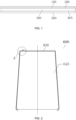
- the PDLC membrane is placed on the negative pressure platform 600 with the back side facing upwards, and the back side liquid crystal activation area of the PDLC membrane is made to coincide with the second transparent area 620 of the negative pressure platform 600, and other areas coincide with the metal material area of the negative pressure platform 600.
- the liquid crystal layer 300 of the PDLC membrane (the back side liquid crystal activation area) is activated.
- the second PET layer 500 and the second electric conduction layer 400 located on the liquid crystal layer 300 are cut and torn off.
- the activated liquid crystal layer 300 is swept off to expose the first electric conduction layer 200 to form a second electrode.
- an infrared laser is used for activation.
- the infrared laser when used for activation, can use the following parameters, wherein
- a carbon dioxide laser is used for cutting.
- the carbon dioxide laser when a carbon dioxide laser is used for cutting, can use the following parameters, wherein
- FIGS. 2 and 3 only exemplarily show the negative pressure platform in the case of activating the side part of the PDLC membrane, where the first transparent area and the second transparent area can be arranged in different ways, such as having different sizes and shapes.
- the front and back sides of the PDLC membrane can be processed in different sizes and shapes, and the processing parameters can also be set differently.
- the terms "front side” and "back side” are only used to distinguish two opposite surfaces of the PDLC membrane, and do not indicate a specific order, structure or the like.
- the activated liquid crystal layer 300 has basically separated from the first electric conduction layer 200 and the second electric conduction layer 400. After the first PET layer 100 and the first electric conduction layer 200 are torn off, a part of the liquid crystal layer 300 can be taken away, and a part of the liquid crystal layer 300 remains in the second electric conduction layer 400. It is possible to use a brush, dust-free cloth or technical foam, etc., to sweep off the remaining part of liquid crystal layer 300, exposing the second electric conduction layer 400, to form the first electrode. Similarly, the same operation can be used for the back side processing steps, which will not be repeated here. However, if the liquid crystal is not activated, the manual wiping, using e.g. alcohol, is required to wipe off the liquid crystal layer 300, which is not only inefficient, but also possible of having the problems, such as incomplete wiping or excessive wiping, which affects the performance of the electrode.
- the manual wiping using e.g. alcohol
- the liquid crystal activation area of the side to be processed of the PDLC membrane coincides with the transparent area 630 of the negative pressure platform 600, and other areas coincide with the metal material area of the negative pressure platform 600.
- the laser light can be made to only penetrate to the transparent area of the negative pressure platform, and not touch the main body area of the negative pressure platform (for example, the metal material area). Since laser light absorbed and reflected by the transparent area is relatively small, a better liquid crystal activation effect is achieved, which is beneficial to the removal of the liquid crystal layer.
- the method for manufacturing a PDLC membrane electrode can reduce the participation by human, increasing the production output, and improving the production efficiency.
- the electrode can be made according to any pattern.
- This embodiment also provides a method for manufacturing a PDLC membrane electrode.
- the method for manufacturing a PDLC membrane electrode comprises the following steps:
- the method for manufacturing a PDLC membrane electrode includes a front side processing step and a back side processing step.
- the PDLC membrane is placed on the negative pressure platform 600 with the front side facing upwards, and the front side liquid crystal activation area of the PDLC membrane is made to coincide with the first transparent area 610 of the negative pressure platform 600, and the other areas coincide with the main body area 640 of the negative pressure platform 600; the liquid crystal layer 300 of the front side liquid crystal activation area of the PDLC membrane is activated; the first PET layer 100 and the first electric conduction layer 200 located on the liquid crystal layer 300 are cut according to the front side half-cut area 10, and the first PET layer 100, the first electric conduction layer 200, and the activated liquid crystal layer 300 are together torn off to expose the second electric conduction layer 400 to form a first electrode.
- the PDLC membrane is placed on the negative pressure platform 600 with the back side facing upwards, and the back side liquid crystal activation area of the PDLC membrane is made to coincide with the second transparent area 620 of the negative pressure platform 600, and other areas coincide with the main body area 640 of the negative pressure platform 600; the liquid crystal layer 300 in the back side liquid crystal activation area of the PDLC membrane is activated; according to the back side half-cut area 20, the second PET layer 500 and the second electric conduction layer 400 located on the liquid crystal layer 300 are cut, and the second PET layer 500, the second electric conduction layer 400 and the activated liquid crystal layer 300 are torn off together to expose the first electric conduction layer 200 to form a second electrode.
- the main body area 640 of the negative pressure platform 600 is a metal material area.
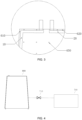
- the negative pressure platform 600 may include a plurality of vent holes 650.
- the main body area 640 of the negative pressure platform comprises a plurality of vent holes 650.
- the transparent area 630 of the negative pressure platform comprises a plurality of vent holes 650.
- both the main body area 640 and the transparent area 630 of the negative pressure platform include a plurality of vent holes 650.
- Each vent hole 650 is in fluid communication with a vacuum device (for example, a vacuum pump) 700.
- the vent hole 650 has a diameter of 0.5 to 3.0 mm, 0.8 to 2.5 mm, or 1 to 2 mm.
- the hole spacing between adjacent vent holes 650 is 10-50 mm, 15-40 mm, or 20-30 mm.
- a valve 710 (such as a solenoid valve) is provided between the vent hole 650 and the vacuum device (such as a vacuum pump) 700.
- the valve 710 can control the fluid communication between the vent hole 650 and the vacuum device 700, for example, opening or cut off the fluid communication between the two.
- the vacuum device 700 provides negative pressure, so that the PDLC membrane to be processed can be smoothly adsorbed on the negative pressure platform 600 without warping, and the start and stop of the vacuum adsorption can be controlled through the PLC control terminal.
- an infrared laser is used for activation.
- the infrared laser when an infrared laser is used for activation, uses the following parameters, wherein
- a carbon dioxide laser is used for cutting.
- the carbon dioxide laser when a carbon dioxide laser is used for cutting, can use the following parameters, wherein
- the PET layer and the electric conduction layer located on the liquid crystal layer are torn off manually or mechanically according to the half-cut area.
- the aforementioned "main body area” is the part of the negative pressure platform 600, which remains after removing the first transparent area 610 and the second transparent area 620.
- the activated liquid crystal layer 300 has been separated from the second electric conduction layer 400. After the first PET layer 100 and the first electric conduction layer 200 are torn off, all of the liquid crystal layer 300 can be taken away, with no liquid crystal layer 300 leaving on the second electric conduction layer 400, therefore there is no need for a sweeping step; and similarly, the same operation can be used for the back side processing step, which will not be repeated here.
- the liquid crystal is not activated or the activation effect is not enough to take away all of the liquid crystal layer 300, it is necessary to manually wipe, with e.g. alcohol, to wipe off the liquid crystal layer 300, or use other methods to clean the remaining liquid crystal layer 300, which is not only inefficient, but also possible of having the problem of incomplete wiping or excessive wiping, which affects the performance of the electrode.
- the PDLC membrane which is obtained by the above processing method, will obtain a resistance value in a stable range when measured by resistance gauge. Especially, when there is no need to sweep the liquid crystal layer, it is possible to eliminate the shortcomings caused by manual wiping of the liquid crystal layer so that the obtained PDLC membrane has a resistance value in a stable range.
- the measured resistance value is 250 ⁇ 50 ohm after the electrode is fabricated by the above method, and the customer standard is usually below 300 ohm.
- the resistance value of the electrode obtained by wiping the liquid crystal layer may be as high as 500 ohm.
- the method for manufacturing a PDLC membrane electrode can have the following advantages.
- the disclosure provides a negative pressure platform 600 that implements the aforementioned method for manufacturing a PDLC membrane electrode.
- the negative pressure platform 600 comprises a transparent area 630 that matches the liquid crystal activation area of the PDLC membrane.
- the main body area 640 of the negative pressure platform 600 may be a metal material area or area made of any other suitable material.
- the negative pressure platform 600 comprises a first transparent area 610 (coinciding with the front side liquid crystal activation area), a second transparent area 620 (coinciding with the back side liquid crystal activation area), and a main body area 640 (for example, a metal material area).
- the material of the metal material region is steel or aluminum.
- the material of the transparent region 630 is transparent organic glass or inorganic glass. In some embodiments, the material of the transparent region 630 is a transparent polyacrylic resin, such as polymethyl methacrylate (acrylic). In some embodiments, the material of the transparent region 630 is transparent polymethyl methacrylate (acrylic) or crystal glass.
- the negative pressure platform 600 may be of a plate-shaped structure.
- the thickness of the negative pressure platform 600 is greater than 15 mm.
- the thickness of the negative pressure platform 600 may be 15 mm, 16 mm, 17 mm, or the like.
- the thickness of the negative pressure platform 600 is generally less than 20 mm.
- the negative pressure platform provided in this example can be applied to the aforementioned method for manufacturing a PDLC membrane electrode.
- the technical advantages and effects achieved by the method for manufacturing a PDLC membrane electrode also include the technical advantages and effects achieved by the negative pressure platform, which is not repeated again here.
- this disclosure also provides a PDLC membrane produced by the aforementioned method for manufacturing a PDLC membrane electrode.
- the PDLC membrane comprises a membrane body, a first electrode (not shown in the drawings), and a second electrode (not shown in the drawings).
- the membrane body comprises a first PET layer 100, a first electric conduction layer 200, a liquid crystal layer 300, a second electric conduction layer 400, and a second PET layer 500, which are included sequentially from top to bottom.
- the first electrode is provided on the second electric conduction layer 400; and the second electrode is provided on the first electric conduction layer 200.
- the PDLC membrane can be manufactured by the aforementioned method for manufacturing a PDLC membrane electrode, wherein the technical advantages and effects achieved by the PDLC membrane also include the technical advantages and effects achieved by the method for manufacturing a PDLC membrane electrode, which will not be repeated again here.
- the present invention provides a method for manufacturing a PDLC membrane electrode, which can reduce participation by human, improve production efficiency, and produce a PDLC membrane with improved electrode performance.
- the electrode can be made according to any patterns.
Landscapes
- Physics & Mathematics (AREA)
- Nonlinear Science (AREA)
- Chemical & Material Sciences (AREA)
- Optics & Photonics (AREA)
- Crystallography & Structural Chemistry (AREA)
- General Physics & Mathematics (AREA)
- Mathematical Physics (AREA)
- Engineering & Computer Science (AREA)
- Dispersion Chemistry (AREA)
- Chemical Kinetics & Catalysis (AREA)
- General Chemical & Material Sciences (AREA)
- Oil, Petroleum & Natural Gas (AREA)
- Plasma & Fusion (AREA)
- Mechanical Engineering (AREA)
- Manufacturing & Machinery (AREA)
- Liquid Crystal (AREA)
- Laminated Bodies (AREA)
- Devices For Indicating Variable Information By Combining Individual Elements (AREA)
Claims (8)
- Ein Verfahren zum Herstellen einer PDLC-Membranelektrode,wobei die polymerdispergierte Flüssigkristall-, PDLC-, Membran aufweist: eine Flüssigkristallschicht (300); elektrische Leitungsschichten (200, 400), die jeweils auf beiden Seiten der Flüssigkristallschicht (300) angeordnet sind; und Basismembranen (100, 500), die jeweils auf Außenseiten der elektrischen Leitungsschichten (200, 400) angeordnet sind; undwobei das Verfahren die folgenden Schritte aufweist:Platzieren der PDLC-Membran auf einer Unterdruckplattform (600), wobei eine zu verarbeitende Seite nach oben weist, wobei die Unterdruckplattform (600) einen transparenten Bereich (630) und einen Hauptkörperbereich (640) aufweist, und Bewirken, dass ein Flüssigkristallaktivierungsbereich der PDLC-Membran mit dem transparenten Bereich (630) der Unterdruckplattform (600) zusammenfällt, und ein anderer Bereich als der Flüssigkristallaktivierungsbereich der PDLC-Membran zu dem Hauptkörperbereich (640) der Unterdruckplattform (600) passt;Aktivieren der Flüssigkristallschicht (300) des Flüssigkristallaktivierungsbereichs der zu verarbeitenden Seite der PDLC-Membran; undSchneiden, gemäß einem Halbschnitt-Bereich, einer Basismembran und einer elektrischen Leitungsschicht, die sich auf der Flüssigkristallschicht (300) befinden, und gemeinsames Abreißen der Basismembran, der elektrischen Leitungsschicht und einer aktivierten Flüssigkristallschicht (300), um eine elektrische Leitungsschicht freizulegen, die sich unter der Flüssigkristallschicht (300) befindet, um eine entsprechende Elektrode zu bilden;wobei ein Halbschnitt-Bereich ein Bereich auf der Unterdruckplattform ist, der verwendet wird, um zu führen, wo die PDLC-Membran geschnitten und abgerissen werden soll;wobei das Verfahren einen Vorderseiten-Verarbeitungsschritt und einen Rückseiten-Verarbeitungsschritt aufweist, wobei während des Vorderseiten-Verarbeitungsschritts die PDLC-Membran auf der Unterdruckplattform (600) platziert wird, wobei eine Vorderseite nach oben weist, und ein Vorderseiten-Flüssigkristallaktivierungsbereich der PDLC-Membran dazu gebracht wird, mit einem ersten transparenten Bereich (610) der Unterdruckplattform (600) zusammenzufallen, und ein anderer Bereich als der Flüssigkristallaktivierungsbereich der PDLC-Membran an dem Hauptkörperbereich (640) der Unterdruckplattform (600) befestigt wird; wobei die Flüssigkristallschicht (300) des Vorderseiten-Flüssigkristallaktivierungsbereichs der PDLC-Membran derart aktiviert wird, dass die aktivierte Flüssigkristallschicht (300) von der zweiten elektrischen Leitungsschicht (400) getrennt wird; wobei gemäß einem Vorderseiten-Halbschnitt-Bereich (10) eine erste Basismembran (100) und eine erste elektrische Leitungsschicht (200), die sich auf der Flüssigkristallschicht (300) befinden, geschnitten werden, und die erste Basismembran (100), die erste elektrische Leitungsschicht (200) und die aktivierte Flüssigkristallschicht (300) gemeinsam abgerissen werden, um eine zweite elektrische Leitungsschicht (400) freizulegen, um eine erste Elektrode zu bilden; undwobei während des Rückseiten-Verarbeitungsschrittsdie PDLC-Membran auf der Unterdruckplattform (600) platziert wird, wobei eine Rückseite nach oben weist, und ein Rückseiten-Flüssigkristallaktivierungsbereich der PDLC-Membran dazu gebracht wird, mit einem zweiten transparenten Bereich (620) der Unterdruckplattform (600) zusammenzufallen, und ein anderer Bereich als der Flüssigkristallaktivierungsbereich der PDLC-Membran an dem Hauptkörperbereich (640) der Unterdruckplattform (600) befestigt wird; wobei die Flüssigkristallschicht (300) des Rückseiten-Flüssigkristallaktivierungsbereichs der PDLC-Membran derart aktiviert wird, dass die aktivierte Flüssigkristallschicht (300) von der ersten elektrischen Leitungsschicht (200) getrennt wird; wobei gemäß einem Rückseiten-Halbschnitt-Bereich (20) eine zweite Basismembran (500) und die zweite elektrische Leitungsschicht (400), die sich auf der Flüssigkristallschicht (300) befinden, geschnitten werden, und die zweite Basismembran (500), die zweite elektrische Leitungsschicht (400) und die aktivierte Flüssigkristallschicht (300) gemeinsam abgerissen werden, um die erste elektrische Leitungsschicht (200) freizulegen, um eine zweite Elektrode zu bilden;wobei in einem Aktivierungsschritt ein Infrarotlaser zur Aktivierung verwendet wird.
- Das Verfahren zum Herstellen einer PDLC-Membranelektrode gemäß Anspruch 1, wobei die Basismembran eine PET-Schicht ist.
- Das Verfahren zum Herstellen einer PDLC-Membranelektrode gemäß Anspruch 1, wobei der Infrarotlaser die folgenden Parameter verwendet, wobeiein Wellenlängenbereich 955~1068 nm beträgt;ein Frequenzbereich 20~80 khz beträgt;ein Energiebereich 1~5 J/s beträgt;ein Fülldichtebereich 0,002~0,05 mm beträgt;ein Verarbeitungsgeschwindigkeitsbereich 500~8000 mm/s beträgt;ein Verarbeitungsdickenbereich 0,05~0,3 mm beträgt;ein Verarbeitungsbreitenbereich 1 - 20 mm beträgt; undein Verarbeitungszeitbereich 2 Stunden beträgt.
- Das Verfahren zum Herstellen einer PDLC-Membranelektrode gemäß einem der Ansprüche 1 - 3, wobei Material des transparenten Bereichs (630) aus transparentem organischem Glas oder anorganischem Glas ausgewählt ist.
- Das Verfahren zum Herstellen einer PDLC-Membranelektrode gemäß Anspruch 4, wobei das Material des transparenten Bereichs (630) aus transparentem Polymethylmethacrylat oder Kristallglas ausgewählt ist.
- Das Verfahren zum Herstellen einer PDLC-Membranelektrode gemäß einem der Ansprüche 1 - 5, wobei der Hauptkörperbereich (640) der Unterdruckplattform (600) ein Metallmaterialbereich ist.
- Das Verfahren zum Herstellen einer PDLC-Membranelektrode gemäß einem der Ansprüche 1 - 6, wobei die Unterdruckplattform (600) eine Mehrzahl von Entlüftungslöchern (650) in Fluidverbindung mit einer Vakuumvorrichtung (700) aufweist, so dass eine zu verarbeitende PDLC-Membran auf der Plattform adsorbiert wird.
- Das Verfahren zum Herstellen einer PDLC-Membranelektrode gemäß einem der Ansprüche 1 - 6, wobei beim Schneiden gemäß dem Halbschnitt-Bereich ein Kohlendioxidlaser zum Schneiden verwendet wird.
Applications Claiming Priority (2)
| Application Number | Priority Date | Filing Date | Title |
|---|---|---|---|
| CN202011470771.9A CN112596291B (zh) | 2020-12-14 | 2020-12-14 | Pdlc膜电极制作方法、负压平台及pdlc膜 |
| PCT/CN2021/075325 WO2022126847A1 (zh) | 2020-12-14 | 2021-02-04 | Pdlc膜电极制作方法、负压平台及pdlc膜 |
Publications (4)
| Publication Number | Publication Date |
|---|---|
| EP4036640A1 EP4036640A1 (de) | 2022-08-03 |
| EP4036640A4 EP4036640A4 (de) | 2022-12-07 |
| EP4036640C0 EP4036640C0 (de) | 2025-05-14 |
| EP4036640B1 true EP4036640B1 (de) | 2025-05-14 |
Family
ID=75196486
Family Applications (1)
| Application Number | Title | Priority Date | Filing Date |
|---|---|---|---|
| EP21865359.0A Active EP4036640B1 (de) | 2020-12-14 | 2021-02-04 | Verfahren zur herstellung einer pdlc-membranelektrode |
Country Status (6)
| Country | Link |
|---|---|
| US (1) | US12253767B2 (de) |
| EP (1) | EP4036640B1 (de) |
| JP (1) | JP7301174B2 (de) |
| KR (1) | KR102769768B1 (de) |
| CN (1) | CN112596291B (de) |
| WO (1) | WO2022126847A1 (de) |
Families Citing this family (2)
| Publication number | Priority date | Publication date | Assignee | Title |
|---|---|---|---|---|
| CN115291444B (zh) * | 2022-09-02 | 2024-03-15 | 上海隆昇光电新材料有限公司 | 分区调光膜、电极制作方法及激光切割装置 |
| CN118417270A (zh) * | 2023-07-31 | 2024-08-02 | 昆山阿利曼自动化激光设备有限公司 | 一种调光膜电极侧液晶的清洗设备及方法 |
Citations (2)
| Publication number | Priority date | Publication date | Assignee | Title |
|---|---|---|---|---|
| JP4655406B2 (ja) * | 2001-05-11 | 2011-03-23 | 株式会社東京精密 | 面発光式吸着テーブル |
| KR102176615B1 (ko) * | 2020-07-03 | 2020-11-09 | (주)디바이스이엔지 | 디스플레이 소자의 트랜스퍼 장치 및 트랜스퍼 방법 |
Family Cites Families (16)
| Publication number | Priority date | Publication date | Assignee | Title |
|---|---|---|---|---|
| JP2001059954A (ja) | 1999-08-23 | 2001-03-06 | Minolta Co Ltd | 熱可逆性記録媒体への画像記録方法 |
| JP2003294950A (ja) | 2002-02-01 | 2003-10-15 | Dainippon Printing Co Ltd | 液晶膜のパターニング方法 |
| JP2004050797A (ja) | 2002-07-24 | 2004-02-19 | Dainippon Printing Co Ltd | 光学素子用原版の製造方法および光学素子用原版 |
| KR100856151B1 (ko) * | 2006-11-06 | 2008-09-03 | 아이디 리써치 피티와이 리미티드 | 고분자 분산형 액정표시장치의 전극 단자부 제조방법 |
| US8828176B2 (en) * | 2010-03-29 | 2014-09-09 | Ravenbrick Llc | Polymer stabilized thermotropic liquid crystal device |
| EP3411456B1 (de) | 2016-02-01 | 2019-11-06 | Central Glass Company, Limited | Polymerdispergierte flüssigkristallglaskonstruktion |
| JP2019184909A (ja) | 2018-04-13 | 2019-10-24 | 凸版印刷株式会社 | 接続具 |
| CN108445667A (zh) | 2018-05-15 | 2018-08-24 | 高志超 | 一种基于pdlc液晶调光膜的电子百叶膜、玻璃及控制系统 |
| CN108957801A (zh) * | 2018-07-19 | 2018-12-07 | 张家港康得新光电材料有限公司 | 一种pdlc膜的电极在线制作方法及设备 |
| KR102721282B1 (ko) | 2018-09-10 | 2024-10-23 | 닛토덴코 가부시키가이샤 | 조광 소자의 제조 방법 |
| KR102785433B1 (ko) | 2018-10-04 | 2025-03-21 | 닛토덴코 가부시키가이샤 | 조광 소자의 제조 방법 |
| JP7310247B2 (ja) | 2019-04-12 | 2023-07-19 | 凸版印刷株式会社 | 調光シート、および、調光シートの製造方法 |
| CN109976062B (zh) | 2019-04-12 | 2025-01-17 | 深圳市宝立创科技有限公司 | 液晶膜切割方法及胆甾相液晶膜 |
| CN110471206A (zh) * | 2019-07-23 | 2019-11-19 | 珠海兴业新材料科技有限公司 | 一种激光直接刻蚀制备有图案和/或文字的pdlc液晶调光膜的方法 |
| CN111308756B (zh) | 2019-12-20 | 2024-03-22 | 章思 | 半切液晶膜及加工方法 |
| CN111381395B (zh) * | 2020-01-21 | 2023-11-28 | 奥提赞光晶(山东)显示科技有限公司 | 一种电控连续变焦透镜、制备方法和曝光系统 |
-
2020
- 2020-12-14 CN CN202011470771.9A patent/CN112596291B/zh active Active
-
2021
- 2021-02-04 JP JP2021572841A patent/JP7301174B2/ja active Active
- 2021-02-04 WO PCT/CN2021/075325 patent/WO2022126847A1/zh not_active Ceased
- 2021-02-04 US US17/766,700 patent/US12253767B2/en active Active
- 2021-02-04 KR KR1020227006720A patent/KR102769768B1/ko active Active
- 2021-02-04 EP EP21865359.0A patent/EP4036640B1/de active Active
Patent Citations (2)
| Publication number | Priority date | Publication date | Assignee | Title |
|---|---|---|---|---|
| JP4655406B2 (ja) * | 2001-05-11 | 2011-03-23 | 株式会社東京精密 | 面発光式吸着テーブル |
| KR102176615B1 (ko) * | 2020-07-03 | 2020-11-09 | (주)디바이스이엔지 | 디스플레이 소자의 트랜스퍼 장치 및 트랜스퍼 방법 |
Also Published As
| Publication number | Publication date |
|---|---|
| EP4036640C0 (de) | 2025-05-14 |
| EP4036640A4 (de) | 2022-12-07 |
| KR20220088676A (ko) | 2022-06-28 |
| WO2022126847A1 (zh) | 2022-06-23 |
| CN112596291A (zh) | 2021-04-02 |
| EP4036640A1 (de) | 2022-08-03 |
| CN112596291B (zh) | 2022-03-18 |
| US12253767B2 (en) | 2025-03-18 |
| KR102769768B1 (ko) | 2025-02-17 |
| JP7301174B2 (ja) | 2023-06-30 |
| US20230194936A1 (en) | 2023-06-22 |
| JP2023510064A (ja) | 2023-03-13 |
Similar Documents
| Publication | Publication Date | Title |
|---|---|---|
| US7202923B2 (en) | Liquid crystal display with polarizer with inclined edge portion | |
| KR100563896B1 (ko) | 액정 패널, 액정 패널 제조 방법, 액정 패널 제조 장치 및 편광판 부착 장치 | |
| EP4036640B1 (de) | Verfahren zur herstellung einer pdlc-membranelektrode | |
| US8419896B2 (en) | Semi-automated reworkability process for de-bonding a display | |
| CN107390436B (zh) | 一种pvb夹胶调光玻璃用调光膜封边工艺 | |
| JP2008201629A (ja) | 電気光学装置の製造方法、基板の分断方法、及び、基板分断装置 | |
| CN101505908A (zh) | 用于柔性显示器应用中的薄的层叠玻璃基底的激光分离 | |
| CN111290174B (zh) | 灯板、背光模组以及显示装置 | |
| JP2010224422A (ja) | 表示装置およびその製造方法 | |
| KR20100056037A (ko) | 액정표시장치의 본딩시스템 | |
| CN103325702A (zh) | 芯片的绑定方法及芯片绑定结构 | |
| CN104166271A (zh) | 一种光学膜层及其制造方法、背光模组和显示装置 | |
| CN101344654B (zh) | 导电胶膜切割工具 | |
| JP3011697B2 (ja) | 高強度タッチパネルとその製造方法 | |
| JP2008225398A (ja) | 液晶表示素子の製造方法 | |
| KR102199052B1 (ko) | 필름 절단 장치 및 필름 절단 방법 | |
| KR102829628B1 (ko) | 고분자 분산 액정 디스플레이의 전극 단자부의 제조방법 | |
| KR102633196B1 (ko) | 스크라이빙 장치 및 스크라이빙 방법 | |
| JP2009282107A (ja) | 表示パネル及びその製造方法 | |
| JP2010054597A (ja) | 表示装置 | |
| CN221940594U (zh) | 掩膜版的固定装置及掩膜版的加工设备 | |
| CN207521900U (zh) | 一种导光板侧贴胶条治具 | |
| JP2018137403A (ja) | 表示装置の製造方法および光照射装置 | |
| JP2023076199A (ja) | 半導体装置の製造方法 | |
| JP2014132309A (ja) | 樹脂基板を用いた電子機器装置の製造方法 |
Legal Events
| Date | Code | Title | Description |
|---|---|---|---|
| STAA | Information on the status of an ep patent application or granted ep patent |
Free format text: STATUS: UNKNOWN |
|
| STAA | Information on the status of an ep patent application or granted ep patent |
Free format text: STATUS: THE INTERNATIONAL PUBLICATION HAS BEEN MADE |
|
| PUAI | Public reference made under article 153(3) epc to a published international application that has entered the european phase |
Free format text: ORIGINAL CODE: 0009012 |
|
| STAA | Information on the status of an ep patent application or granted ep patent |
Free format text: STATUS: REQUEST FOR EXAMINATION WAS MADE |
|
| 17P | Request for examination filed |
Effective date: 20220318 |
|
| AK | Designated contracting states |
Kind code of ref document: A1 Designated state(s): AL AT BE BG CH CY CZ DE DK EE ES FI FR GB GR HR HU IE IS IT LI LT LU LV MC MK MT NL NO PL PT RO RS SE SI SK SM TR |
|
| REG | Reference to a national code |
Ref country code: DE Free format text: PREVIOUS MAIN CLASS: G02F0001130000 Ipc: G02F0001133400 Ref country code: DE Ref legal event code: R079 Ref document number: 602021030919 Country of ref document: DE Free format text: PREVIOUS MAIN CLASS: G02F0001130000 Ipc: G02F0001133400 |
|
| STAA | Information on the status of an ep patent application or granted ep patent |
Free format text: STATUS: EXAMINATION IS IN PROGRESS |
|
| A4 | Supplementary search report drawn up and despatched |
Effective date: 20221108 |
|
| RIC1 | Information provided on ipc code assigned before grant |
Ipc: G02F 1/1345 20060101ALI20221102BHEP Ipc: G02F 1/1333 20060101ALI20221102BHEP Ipc: G02F 1/1334 20060101AFI20221102BHEP |
|
| 17Q | First examination report despatched |
Effective date: 20221122 |
|
| GRAP | Despatch of communication of intention to grant a patent |
Free format text: ORIGINAL CODE: EPIDOSNIGR1 |
|
| STAA | Information on the status of an ep patent application or granted ep patent |
Free format text: STATUS: GRANT OF PATENT IS INTENDED |
|
| INTG | Intention to grant announced |
Effective date: 20241205 |
|
| GRAS | Grant fee paid |
Free format text: ORIGINAL CODE: EPIDOSNIGR3 |
|
| GRAA | (expected) grant |
Free format text: ORIGINAL CODE: 0009210 |
|
| STAA | Information on the status of an ep patent application or granted ep patent |
Free format text: STATUS: THE PATENT HAS BEEN GRANTED |
|
| AK | Designated contracting states |
Kind code of ref document: B1 Designated state(s): AL AT BE BG CH CY CZ DE DK EE ES FI FR GB GR HR HU IE IS IT LI LT LU LV MC MK MT NL NO PL PT RO RS SE SI SK SM TR |
|
| REG | Reference to a national code |
Ref country code: GB Ref legal event code: FG4D |
|
| REG | Reference to a national code |
Ref country code: CH Ref legal event code: EP |
|
| REG | Reference to a national code |
Ref country code: IE Ref legal event code: FG4D |
|
| REG | Reference to a national code |
Ref country code: DE Ref legal event code: R096 Ref document number: 602021030919 Country of ref document: DE |
|
| U01 | Request for unitary effect filed |
Effective date: 20250606 |
|
| U07 | Unitary effect registered |
Designated state(s): AT BE BG DE DK EE FI FR IT LT LU LV MT NL PT RO SE SI Effective date: 20250616 |
|
| PG25 | Lapsed in a contracting state [announced via postgrant information from national office to epo] |
Ref country code: ES Free format text: LAPSE BECAUSE OF FAILURE TO SUBMIT A TRANSLATION OF THE DESCRIPTION OR TO PAY THE FEE WITHIN THE PRESCRIBED TIME-LIMIT Effective date: 20250514 |
|
| PG25 | Lapsed in a contracting state [announced via postgrant information from national office to epo] |
Ref country code: GR Free format text: LAPSE BECAUSE OF FAILURE TO SUBMIT A TRANSLATION OF THE DESCRIPTION OR TO PAY THE FEE WITHIN THE PRESCRIBED TIME-LIMIT Effective date: 20250815 Ref country code: NO Free format text: LAPSE BECAUSE OF FAILURE TO SUBMIT A TRANSLATION OF THE DESCRIPTION OR TO PAY THE FEE WITHIN THE PRESCRIBED TIME-LIMIT Effective date: 20250814 |
|
| PG25 | Lapsed in a contracting state [announced via postgrant information from national office to epo] |
Ref country code: PL Free format text: LAPSE BECAUSE OF FAILURE TO SUBMIT A TRANSLATION OF THE DESCRIPTION OR TO PAY THE FEE WITHIN THE PRESCRIBED TIME-LIMIT Effective date: 20250514 |
|
| PG25 | Lapsed in a contracting state [announced via postgrant information from national office to epo] |
Ref country code: HR Free format text: LAPSE BECAUSE OF FAILURE TO SUBMIT A TRANSLATION OF THE DESCRIPTION OR TO PAY THE FEE WITHIN THE PRESCRIBED TIME-LIMIT Effective date: 20250514 |
|
| PG25 | Lapsed in a contracting state [announced via postgrant information from national office to epo] |
Ref country code: RS Free format text: LAPSE BECAUSE OF FAILURE TO SUBMIT A TRANSLATION OF THE DESCRIPTION OR TO PAY THE FEE WITHIN THE PRESCRIBED TIME-LIMIT Effective date: 20250814 |
|
| PG25 | Lapsed in a contracting state [announced via postgrant information from national office to epo] |
Ref country code: IS Free format text: LAPSE BECAUSE OF FAILURE TO SUBMIT A TRANSLATION OF THE DESCRIPTION OR TO PAY THE FEE WITHIN THE PRESCRIBED TIME-LIMIT Effective date: 20250914 |