EP4020533A2 - Halbleiterbauelement und herstellungsverfahren dafür - Google Patents
Halbleiterbauelement und herstellungsverfahren dafür Download PDFInfo
- Publication number
- EP4020533A2 EP4020533A2 EP21213256.7A EP21213256A EP4020533A2 EP 4020533 A2 EP4020533 A2 EP 4020533A2 EP 21213256 A EP21213256 A EP 21213256A EP 4020533 A2 EP4020533 A2 EP 4020533A2
- Authority
- EP
- European Patent Office
- Prior art keywords
- electronic component
- film substrate
- semiconductor device
- reinforcement member
- adhesive
- Prior art date
- Legal status (The legal status is an assumption and is not a legal conclusion. Google has not performed a legal analysis and makes no representation as to the accuracy of the status listed.)
- Pending
Links
Images



Classifications
-
- H—ELECTRICITY
- H10—SEMICONDUCTOR DEVICES; ELECTRIC SOLID-STATE DEVICES NOT OTHERWISE PROVIDED FOR
- H10W—GENERIC PACKAGES, INTERCONNECTIONS, CONNECTORS OR OTHER CONSTRUCTIONAL DETAILS OF DEVICES COVERED BY CLASS H10
- H10W70/00—Package substrates; Interposers; Redistribution layers [RDL]
- H10W70/60—Insulating or insulated package substrates; Interposers; Redistribution layers
- H10W70/67—Insulating or insulated package substrates; Interposers; Redistribution layers characterised by their insulating layers or insulating parts
- H10W70/68—Shapes or dispositions thereof
- H10W70/685—Shapes or dispositions thereof comprising multiple insulating layers
-
- H—ELECTRICITY
- H10—SEMICONDUCTOR DEVICES; ELECTRIC SOLID-STATE DEVICES NOT OTHERWISE PROVIDED FOR
- H10W—GENERIC PACKAGES, INTERCONNECTIONS, CONNECTORS OR OTHER CONSTRUCTIONAL DETAILS OF DEVICES COVERED BY CLASS H10
- H10W70/00—Package substrates; Interposers; Redistribution layers [RDL]
- H10W70/01—Manufacture or treatment
- H10W70/05—Manufacture or treatment of insulating or insulated package substrates, or of interposers, or of redistribution layers
- H10W70/08—Manufacture or treatment of insulating or insulated package substrates, or of interposers, or of redistribution layers by depositing layers on the chip or wafer, e.g. "chip-first" RDLs
- H10W70/09—Manufacture or treatment of insulating or insulated package substrates, or of interposers, or of redistribution layers by depositing layers on the chip or wafer, e.g. "chip-first" RDLs extending onto an encapsulation that laterally surrounds the chip or wafer, e.g. fan-out wafer level package [FOWLP] RDLs
-
- H—ELECTRICITY
- H10—SEMICONDUCTOR DEVICES; ELECTRIC SOLID-STATE DEVICES NOT OTHERWISE PROVIDED FOR
- H10W—GENERIC PACKAGES, INTERCONNECTIONS, CONNECTORS OR OTHER CONSTRUCTIONAL DETAILS OF DEVICES COVERED BY CLASS H10
- H10W42/00—Arrangements for protection of devices
- H10W42/121—Arrangements for protection of devices protecting against mechanical damage
-
- H—ELECTRICITY
- H10—SEMICONDUCTOR DEVICES; ELECTRIC SOLID-STATE DEVICES NOT OTHERWISE PROVIDED FOR
- H10W—GENERIC PACKAGES, INTERCONNECTIONS, CONNECTORS OR OTHER CONSTRUCTIONAL DETAILS OF DEVICES COVERED BY CLASS H10
- H10W42/00—Arrangements for protection of devices
- H10W42/20—Arrangements for protection of devices protecting against electromagnetic or particle radiation, e.g. light, X-rays, gamma-rays or electrons
- H10W42/261—Arrangements for protection of devices protecting against electromagnetic or particle radiation, e.g. light, X-rays, gamma-rays or electrons characterised by their shapes or dispositions
- H10W42/276—Arrangements for protection of devices protecting against electromagnetic or particle radiation, e.g. light, X-rays, gamma-rays or electrons characterised by their shapes or dispositions the arrangements being on an external surface of the package, e.g. on the outer surface of an encapsulation
-
- H—ELECTRICITY
- H10—SEMICONDUCTOR DEVICES; ELECTRIC SOLID-STATE DEVICES NOT OTHERWISE PROVIDED FOR
- H10W—GENERIC PACKAGES, INTERCONNECTIONS, CONNECTORS OR OTHER CONSTRUCTIONAL DETAILS OF DEVICES COVERED BY CLASS H10
- H10W74/00—Encapsulations, e.g. protective coatings
- H10W74/01—Manufacture or treatment
-
- H—ELECTRICITY
- H10—SEMICONDUCTOR DEVICES; ELECTRIC SOLID-STATE DEVICES NOT OTHERWISE PROVIDED FOR
- H10W—GENERIC PACKAGES, INTERCONNECTIONS, CONNECTORS OR OTHER CONSTRUCTIONAL DETAILS OF DEVICES COVERED BY CLASS H10
- H10W74/00—Encapsulations, e.g. protective coatings
- H10W74/10—Encapsulations, e.g. protective coatings characterised by their shape or disposition
- H10W74/111—Encapsulations, e.g. protective coatings characterised by their shape or disposition the semiconductor body being completely enclosed
- H10W74/114—Encapsulations, e.g. protective coatings characterised by their shape or disposition the semiconductor body being completely enclosed by a substrate and the encapsulations
-
- H—ELECTRICITY
- H10—SEMICONDUCTOR DEVICES; ELECTRIC SOLID-STATE DEVICES NOT OTHERWISE PROVIDED FOR
- H10W—GENERIC PACKAGES, INTERCONNECTIONS, CONNECTORS OR OTHER CONSTRUCTIONAL DETAILS OF DEVICES COVERED BY CLASS H10
- H10W76/00—Containers; Fillings or auxiliary members therefor; Seals
- H10W76/40—Fillings or auxiliary members in containers, e.g. centering rings
-
- H—ELECTRICITY
- H10—SEMICONDUCTOR DEVICES; ELECTRIC SOLID-STATE DEVICES NOT OTHERWISE PROVIDED FOR
- H10W—GENERIC PACKAGES, INTERCONNECTIONS, CONNECTORS OR OTHER CONSTRUCTIONAL DETAILS OF DEVICES COVERED BY CLASS H10
- H10W70/00—Package substrates; Interposers; Redistribution layers [RDL]
- H10W70/01—Manufacture or treatment
- H10W70/05—Manufacture or treatment of insulating or insulated package substrates, or of interposers, or of redistribution layers
- H10W70/093—Connecting or disconnecting other interconnections thereto or therefrom, e.g. connecting bond wires or bumps
-
- H—ELECTRICITY
- H10—SEMICONDUCTOR DEVICES; ELECTRIC SOLID-STATE DEVICES NOT OTHERWISE PROVIDED FOR
- H10W—GENERIC PACKAGES, INTERCONNECTIONS, CONNECTORS OR OTHER CONSTRUCTIONAL DETAILS OF DEVICES COVERED BY CLASS H10
- H10W72/00—Interconnections or connectors in packages
- H10W72/071—Connecting or disconnecting
- H10W72/073—Connecting or disconnecting of die-attach connectors
-
- H—ELECTRICITY
- H10—SEMICONDUCTOR DEVICES; ELECTRIC SOLID-STATE DEVICES NOT OTHERWISE PROVIDED FOR
- H10W—GENERIC PACKAGES, INTERCONNECTIONS, CONNECTORS OR OTHER CONSTRUCTIONAL DETAILS OF DEVICES COVERED BY CLASS H10
- H10W72/00—Interconnections or connectors in packages
- H10W72/30—Die-attach connectors
- H10W72/351—Materials of die-attach connectors
- H10W72/352—Materials of die-attach connectors comprising metals or metalloids, e.g. solders
-
- H—ELECTRICITY
- H10—SEMICONDUCTOR DEVICES; ELECTRIC SOLID-STATE DEVICES NOT OTHERWISE PROVIDED FOR
- H10W—GENERIC PACKAGES, INTERCONNECTIONS, CONNECTORS OR OTHER CONSTRUCTIONAL DETAILS OF DEVICES COVERED BY CLASS H10
- H10W72/00—Interconnections or connectors in packages
- H10W72/851—Dispositions of multiple connectors or interconnections
- H10W72/874—On different surfaces
-
- H—ELECTRICITY
- H10—SEMICONDUCTOR DEVICES; ELECTRIC SOLID-STATE DEVICES NOT OTHERWISE PROVIDED FOR
- H10W—GENERIC PACKAGES, INTERCONNECTIONS, CONNECTORS OR OTHER CONSTRUCTIONAL DETAILS OF DEVICES COVERED BY CLASS H10
- H10W72/00—Interconnections or connectors in packages
- H10W72/90—Bond pads, in general
- H10W72/941—Dispositions of bond pads
- H10W72/9413—Dispositions of bond pads on encapsulations
-
- H—ELECTRICITY
- H10—SEMICONDUCTOR DEVICES; ELECTRIC SOLID-STATE DEVICES NOT OTHERWISE PROVIDED FOR
- H10W—GENERIC PACKAGES, INTERCONNECTIONS, CONNECTORS OR OTHER CONSTRUCTIONAL DETAILS OF DEVICES COVERED BY CLASS H10
- H10W72/00—Interconnections or connectors in packages
- H10W72/90—Bond pads, in general
- H10W72/941—Dispositions of bond pads
- H10W72/944—Dispositions of multiple bond pads
-
- H—ELECTRICITY
- H10—SEMICONDUCTOR DEVICES; ELECTRIC SOLID-STATE DEVICES NOT OTHERWISE PROVIDED FOR
- H10W—GENERIC PACKAGES, INTERCONNECTIONS, CONNECTORS OR OTHER CONSTRUCTIONAL DETAILS OF DEVICES COVERED BY CLASS H10
- H10W90/00—Package configurations
- H10W90/701—Package configurations characterised by the relative positions of pads or connectors relative to package parts
- H10W90/731—Package configurations characterised by the relative positions of pads or connectors relative to package parts of die-attach connectors
- H10W90/734—Package configurations characterised by the relative positions of pads or connectors relative to package parts of die-attach connectors between a chip and a stacked insulating package substrate, interposer or RDL
Definitions
- a certain aspect of the embodiment discussed herein is related to semiconductor devices and methods of manufacturing the same.
- a wiring layer is formed on the other surface of the film substrate.
- the film substrate is thin. Therefore, in an area where no electronic component is mounted (which may be hereinafter referred to as "non-mounting area"), the film substrate is low in stiffness and is likely to warp because of its own weight alone. The warp of the non-mounting area may apply an excessive stress to a conductive pattern to cause a crack in the conductive pattern.
- the present disclosure has an object of providing a semiconductor device in which the warp of a film substrate is controlled and a method of manufacturing such a semiconductor device.
- a semiconductor device includes a film substrate, an adhesive on a first surface of the film substrate, an electronic component on the adhesive, a wiring layer on a second surface of the film substrate opposite from the first surface, and a reinforcement member in an area around the electronic component on the adhesive.
- the wiring layer is connected to the electronic component through a via hole piercing through the film substrate and the adhesive.
- the reinforcement member has a thickness smaller than the thickness of the electronic component.
- first side the side of the film substrate of a semiconductor device on which side an electronic component is mounted
- second side the opposite side of the film substrate
- first surface a surface of the film substrate on which an electronic component is mounted
- second surface a surface of the film substrate on which an electronic component is mounted
- first surface a surface of the film substrate on which an electronic component is mounted
- second surface a surface of the film substrate
- FIGS. 1A and 1B are diagrams illustrating a semiconductor device 1 according to the embodiment.
- FIG. 1A is a sectional view of the semiconductor device 1 taken along the line IA-IA of FIG. 1B.
- FIG. 1B is a lower side (bottom) view of the semiconductor device 1.
- the semiconductor device 1 includes a film substrate 10, an adhesive 20, an electronic component 30, a reinforcement member 40 (an insulating layer), and a wiring layer 53.
- the adhesive 20 is provided on a first surface 11 of the film substrate 10.
- materials for the film substrate 10 include resins such as polyimide, epoxy, and acrylic resins.
- the thickness of the film substrate 10 is, for example, approximately 50 ⁇ m to approximately 100 ⁇ m.
- the material of the adhesive 20 is a thermosetting resin, and includes, for example, epoxy as a main component.
- a via hole 21 is formed in a laminate (layered structure) of the film substrate 10 and the adhesive 20.
- the via hole 21 has an inverted truncated cone shape, tapering from the film substrate 10 side end to the adhesive 20 side end with an inclined lateral surface, so that the diameter of the via hole 21 is greater at the upper edge, or the film substrate 10 side end, than at the lower edge, or the adhesive 20 side end.
- Two or more via holes 21 may be formed.
- one or more via holes 21 may be collectively referred to as "via hole 21.”
- the electronic component 30 is fixed to the film substrate 10 by the adhesive 20.
- the electronic component 30 include a semiconductor element (device) serving as an active element (for example, a silicon chip such as a central processing unit (CPU)), an insulated-gate bipolar transistor (IGBT), a metal-oxide-semiconductor field-effect transistor (MOSFET), and a diode.
- the electronic component 30 is a semiconductor element having electrodes provided on both the top side and the bottom side. According to this embodiment, an electrode 31 is provided on the first surface of the electronic component 30 and an electrode 32 is provided on the second surface of the electronic component 30. Two or more electrodes 32 may be provided. Hereinafter, one or more electrodes 32 may be collectively referred to as "electrode 32.” The electrode 32 is so placed as to correspond to the via hole 21.
- the reinforcement member 40 is fixed to the film substrate 10 by the adhesive 20.
- the reinforcement member 40 is, for example, an insulating film in which an opening 40a corresponding to the electronic component 30 is formed.
- the reinforcement member 40 surrounds the electronic component 30.
- the outer edge of the reinforcement member 40 substantially coincides with the outer edge of the film substrate 10.
- the material of the reinforcement member 40 may be the same as the material of the film substrate 10. Examples of materials for the reinforcement member 40 include resins such as polyimide, epoxy, and acrylic resins.
- the thickness of the reinforcement member 40 may be equal to the thickness of the film substrate 10.
- the thickness of the reinforcement member 40 may be greater than the thickness of the film substrate 10.
- the thickness of the reinforcement member 40 is, for example, approximately 100 ⁇ m to approximately 150 ⁇ m.
- the thickness of the reinforcement member 40 is preferably smaller than the thickness (height) of the electronic component 30.
- the electrode 31 is placed opposite a mounting substrate such as a wiring substrate and is soldered to a conductive pattern on the mounting substrate. Therefore, a lower surface 40b of the reinforcement member 40 is preferably positioned higher (closer to the wiring layer 53) than the lower surface of the electronic component 30. That is, the electronic component 30 preferably protrudes relative to the lower surface 40b of the reinforcement member 40.
- the wiring layer 53 is formed (fills) in the via hole 21 and is formed on a second surface 12 of the film substrate 10.
- the wiring layer 53 includes a seed layer 51 and a plating layer 52 formed on the seed layer 51.
- the seed layer 51 and the plating layer 52 are, for example, copper layers.
- a surface treatment layer may be formed on a surface of the wiring layer 53. Examples of surface treatment layers include a gold (Au) layer, a nickel (Ni)/Au layer (a laminated metal layer of a Ni layer and a Au layer that are stacked in this order), and a Ni/palladium (Pd)/Au layer (a laminated metal layer of a Ni layer, a Pd layer, and a Au layer that are stacked in this order).
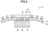
- FIG. 2 is a sectional view of a semiconductor device 9 according to the reference example.
- the semiconductor device 9 has the same configuration as the semiconductor device 1 of this embodiment except that the reinforcement member 40 is not provided.
- the semiconductor device 1 can have high stiffness because the reinforcement member 40 is provided. Therefore, while the semiconductor device 9 is likely to have a warp caused in a non-mounting region because of thermal contraction or the like as illustrated in FIG. 2 , the semiconductor device 1 can control warping.
- warping By controlling warping, it is possible to reduce or eliminate cracks in the wiring layer 53 to achieve high reliability. Furthermore, because warping is controlled, it is easy to align the semiconductor device 1 with high accuracy when mounting the semiconductor device 1 on a mounting substrate. Therefore, the semiconductor device 1 is easily usable with smaller mounting substrates. Furthermore, by controlling warping, it is possible to avoid unnecessary contact between an end of the semiconductor device 1 and a conductive pattern on a mounting substrate.
- the single wiring layer 53 is provided according to this embodiment, two or more wiring layers may be provided on the film substrate 10. That is, a multilayer wiring structure may be provided.
- the reinforcement member 40 does not have to be in contact with the electronic component 30. In the plan view, there may be a gap between the reinforcement member 40 and the electronic component 30.
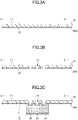
- FIGS. 3A through 3K are sectional views illustrating a method of manufacturing the semiconductor device 1 according to this embodiment.
- the film substrate 10 is prepared.
- the size of the film substrate 10 prepared here is a large size corresponding to multiple semiconductor devices 1, and this film substrate 10 is ultimately cut along cutting lines C to be divided into individual pieces.
- an uncured adhesive 20A is provided on the first surface 11 of the film substrate 10.
- the adhesive 20A may be provided by, for example, spin coating.
- a film adhesive may be applied as the adhesive 20A.
- the via hole 21 is formed in a laminate of the film substrate 10 and the adhesive 20A.
- the via hole 21 may be formed by, for example, emitting a laser beam onto the laminate from the film substrate 10 side.
- the electronic component 30 is attached to the adhesive 20A.
- the electronic component 30 has the electrode 31 on the first surface and the electrode 32 on the second surface.
- the electrode 32 is aligned with the via hole 21.
- the insulating reinforcement member 40 is attached to the adhesive 20A in an area around the electronic component 30.
- the reinforcement member 40 is, for example, an insulating film in which an opening corresponding to the electronic component 30 is formed.
- the cured adhesive 20 is obtained from the adhesive 20A.
- the adhesive 20A cures to firmly fix the electronic component 30 and the reinforcement member 40 to the film substrate 10.
- the seed layer 51 is formed on the second surface 12 of the film substrate 10, a surface of the laminate defining the side of the via hole 21 (a side surface 21a of the via hole 21), and a surface 32a of the electrode 32 of the electronic component 30 exposed in the via hole 21.
- the seed layer 51 may be formed by, for example, sputtering.
- a spacer 91 contacting the lower surface of the reinforcement member 40 is placed in an area around the electronic component 30.
- the spacer 91 may be a recess structure that can accommodate the electronic component 30, or may be a laminate of multiple spacers.
- materials for the spacer 91 include resins such as polyimide, epoxy, and acrylic resins. Resin and metal may be used alone or in combination as the material of the spacer 91.
- the same insulating film as used as the reinforcement member 40 may be used as the spacer 91.
- a protective film 92 is placed under the spacer 91.
- materials for the protective film 92 include polyimide, polyolefin, and polyvinyl chloride.
- the plating layer 52 is formed on the seed layer 51.
- the spacer 91 and the protective film 92 are provided under the film substrate 10, the electronic component 30 including the electrode 31 is protected from an electrolyte.
- a resist layer (not depicted) in which a wiring pattern is formed is formed on the plating layer 52.
- a dry film resist or the like may be used as the resist layer.
- the resist layer may be exposed to light and developed to have a wiring pattern formed in the resist layer.
- the plating layer 52 and the seed layer 51 are etched using the resist layer as a mask.
- the wiring layer 53 is obtained from the plating layer 52 and the seed layer 51.
- the wiring layer 53 may be formed by, for example, a semiadditive process.
- a surface treatment layer may be formed on the wiring layer 53. Other plating may be performed on the wiring layer 53. During etching and plating as well, the electronic component 30 is protected by the spacer 91 and the protective film 92.
- FIG. 3J is cut along the cutting lines C into individual pieces.
- the semiconductor device 1 is obtained. While the single semiconductor device 1 is depicted in FIG. 3K , multiple semiconductor devices 1 are obtained from the structure illustrated in FIG. 3J .
- FIGS. 4A and 4B are lower side (bottom) views of semiconductor devices according to variations of the embodiment.
- a semiconductor device 2 of a first variation illustrated in FIG. 4A four electronic components 30 are arranged in a matrix in the substantial center of the first surface 11 of the film substrate 10.
- the reinforcement member 40 is so provided as to surround the four electronic components 30. Furthermore, the reinforcement member 40 is also provided between adjacent electronic components 30. In this case, four openings 40a corresponding to the four electronic components 30 are formed in the reinforcement member 40.
- a semiconductor device 3 of a second variation illustrated in FIG. 4B four electronic components 30 are arranged in a matrix in the substantial center of the first surface 11 of the film substrate 10.
- the reinforcement member 40 is so provided as to surround the four electronic components 30, and the adhesive 20 is exposed between adjacent electronic components 30.
Landscapes
- Die Bonding (AREA)
- Structure Of Printed Boards (AREA)
Applications Claiming Priority (1)
| Application Number | Priority Date | Filing Date | Title |
|---|---|---|---|
| JP2020217444A JP7516242B2 (ja) | 2020-12-25 | 2020-12-25 | 半導体装置及びその製造方法 |
Publications (2)
| Publication Number | Publication Date |
|---|---|
| EP4020533A2 true EP4020533A2 (de) | 2022-06-29 |
| EP4020533A3 EP4020533A3 (de) | 2022-09-21 |
Family
ID=79231012
Family Applications (1)
| Application Number | Title | Priority Date | Filing Date |
|---|---|---|---|
| EP21213256.7A Pending EP4020533A3 (de) | 2020-12-25 | 2021-12-08 | Halbleiterbauelement und herstellungsverfahren dafür |
Country Status (3)
| Country | Link |
|---|---|
| US (1) | US11742272B2 (de) |
| EP (1) | EP4020533A3 (de) |
| JP (1) | JP7516242B2 (de) |
Citations (3)
| Publication number | Priority date | Publication date | Assignee | Title |
|---|---|---|---|---|
| US8049338B2 (en) | 2006-04-07 | 2011-11-01 | General Electric Company | Power semiconductor module and fabrication method |
| JP2019114759A (ja) | 2017-12-26 | 2019-07-11 | 太陽誘電株式会社 | 回路モジュール、回路モジュールの製造方法 |
| JP2020155640A (ja) | 2019-03-20 | 2020-09-24 | 太陽誘電株式会社 | モジュールおよびその製造方法 |
Family Cites Families (11)
| Publication number | Priority date | Publication date | Assignee | Title |
|---|---|---|---|---|
| JPS5670655A (en) * | 1979-11-15 | 1981-06-12 | Matsushita Electric Ind Co Ltd | Manufacture of electronic circuit mounting device |
| US5353498A (en) * | 1993-02-08 | 1994-10-11 | General Electric Company | Method for fabricating an integrated circuit module |
| KR100514558B1 (ko) | 1998-09-09 | 2005-09-13 | 세이코 엡슨 가부시키가이샤 | 반도체 장치 및 그 제조방법, 회로기판 및 전자기기 |
| JP3301985B2 (ja) * | 1998-10-07 | 2002-07-15 | 新光電気工業株式会社 | 半導体装置の製造方法 |
| US6570245B1 (en) | 2000-03-09 | 2003-05-27 | Intel Corporation | Stress shield for microelectronic dice |
| TWI237883B (en) | 2004-05-11 | 2005-08-11 | Via Tech Inc | Chip embedded package structure and process thereof |
| JP2010027825A (ja) | 2008-07-18 | 2010-02-04 | Sharp Corp | 実装基板、実装基板セット、パネルユニット、および実装基板セットの製造方法 |
| JP2015088544A (ja) | 2013-10-29 | 2015-05-07 | イビデン株式会社 | プリント配線板の製造方法およびプリント配線板 |
| JP2019016683A (ja) | 2017-07-06 | 2019-01-31 | 新光電気工業株式会社 | 配線基板及びその製造方法、半導体パッケージ |
| JP2020004905A (ja) | 2018-06-29 | 2020-01-09 | 太陽誘電株式会社 | 半導体モジュール |
| JP2020013877A (ja) | 2018-07-18 | 2020-01-23 | 太陽誘電株式会社 | 半導体モジュール |
-
2020
- 2020-12-25 JP JP2020217444A patent/JP7516242B2/ja active Active
-
2021
- 2021-11-26 US US17/456,612 patent/US11742272B2/en active Active
- 2021-12-08 EP EP21213256.7A patent/EP4020533A3/de active Pending
Patent Citations (3)
| Publication number | Priority date | Publication date | Assignee | Title |
|---|---|---|---|---|
| US8049338B2 (en) | 2006-04-07 | 2011-11-01 | General Electric Company | Power semiconductor module and fabrication method |
| JP2019114759A (ja) | 2017-12-26 | 2019-07-11 | 太陽誘電株式会社 | 回路モジュール、回路モジュールの製造方法 |
| JP2020155640A (ja) | 2019-03-20 | 2020-09-24 | 太陽誘電株式会社 | モジュールおよびその製造方法 |
Also Published As
| Publication number | Publication date |
|---|---|
| JP7516242B2 (ja) | 2024-07-16 |
| US20220208668A1 (en) | 2022-06-30 |
| US11742272B2 (en) | 2023-08-29 |
| JP2022102611A (ja) | 2022-07-07 |
| EP4020533A3 (de) | 2022-09-21 |
Similar Documents
| Publication | Publication Date | Title |
|---|---|---|
| KR100663393B1 (ko) | 반도체패키지 및 그 제조방법 | |
| KR100595889B1 (ko) | 상하도전층의 도통부를 갖는 반도체장치 및 그 제조방법 | |
| US9041211B2 (en) | Semiconductor package and method for manufacturing the semiconductor package embedded with semiconductor chip | |
| TWI762052B (zh) | 封裝方法、面板組件以及晶圓封裝體 | |
| US10978417B2 (en) | Wiring structure and method for manufacturing the same | |
| JP5942823B2 (ja) | 電子部品装置の製造方法、電子部品装置及び電子装置 | |
| JP3795040B2 (ja) | 半導体装置の製造方法 | |
| JP3844467B2 (ja) | 半導体装置及びその製造方法 | |
| US20150223318A1 (en) | Multilayer wiring board | |
| KR20090029660A (ko) | 반도체 장치의 제조 방법 | |
| US20070228554A1 (en) | Semiconductor device and manufacturing method thereof | |
| JP5903920B2 (ja) | 半導体装置の製造方法及び電子装置の製造方法 | |
| US9510447B2 (en) | Printed wiring board and method for manufacturing the same | |
| JP3618330B2 (ja) | 半導体装置及びその製造方法 | |
| TW201517224A (zh) | 半導體裝置以及其製備方法 | |
| EP4020533A2 (de) | Halbleiterbauelement und herstellungsverfahren dafür | |
| JP3925503B2 (ja) | 半導体装置 | |
| JP4056360B2 (ja) | 半導体装置及びその製造方法 | |
| JP2008288481A (ja) | 半導体装置およびその製造方法 | |
| JP2006100666A (ja) | 半導体装置及びその製造方法 | |
| JP2005044989A (ja) | 半導体パッケージ及びその製造方法 | |
| JP4214969B2 (ja) | 半導体装置の製造方法 | |
| US20220399283A1 (en) | Semiconductor device package and method for manufacturing the same | |
| JP4131256B2 (ja) | 半導体装置及びその製造方法 | |
| JP2020174203A (ja) | 半導体装置 |
Legal Events
| Date | Code | Title | Description |
|---|---|---|---|
| PUAI | Public reference made under article 153(3) epc to a published international application that has entered the european phase |
Free format text: ORIGINAL CODE: 0009012 |
|
| STAA | Information on the status of an ep patent application or granted ep patent |
Free format text: STATUS: THE APPLICATION HAS BEEN PUBLISHED |
|
| AK | Designated contracting states |
Kind code of ref document: A2 Designated state(s): AL AT BE BG CH CY CZ DE DK EE ES FI FR GB GR HR HU IE IS IT LI LT LU LV MC MK MT NL NO PL PT RO RS SE SI SK SM TR |
|
| PUAL | Search report despatched |
Free format text: ORIGINAL CODE: 0009013 |
|
| AK | Designated contracting states |
Kind code of ref document: A3 Designated state(s): AL AT BE BG CH CY CZ DE DK EE ES FI FR GB GR HR HU IE IS IT LI LT LU LV MC MK MT NL NO PL PT RO RS SE SI SK SM TR |
|
| RIC1 | Information provided on ipc code assigned before grant |
Ipc: H01L 23/16 20060101ALI20220816BHEP Ipc: H01L 21/60 20060101AFI20220816BHEP |
|
| STAA | Information on the status of an ep patent application or granted ep patent |
Free format text: STATUS: REQUEST FOR EXAMINATION WAS MADE |
|
| 17P | Request for examination filed |
Effective date: 20221116 |