EP3975425A2 - Zur pegelumwandlung befähigte klinke - Google Patents
Zur pegelumwandlung befähigte klinke Download PDFInfo
- Publication number
- EP3975425A2 EP3975425A2 EP21186808.8A EP21186808A EP3975425A2 EP 3975425 A2 EP3975425 A2 EP 3975425A2 EP 21186808 A EP21186808 A EP 21186808A EP 3975425 A2 EP3975425 A2 EP 3975425A2
- Authority
- EP
- European Patent Office
- Prior art keywords
- latch
- transistor
- signal
- logic value
- output signal
- Prior art date
- Legal status (The legal status is an assumption and is not a legal conclusion. Google has not performed a legal analysis and makes no representation as to the accuracy of the status listed.)
- Pending
Links
- 230000004044 response Effects 0.000 claims abstract description 26
- 238000010586 diagram Methods 0.000 description 24
- 102100036285 25-hydroxyvitamin D-1 alpha hydroxylase, mitochondrial Human genes 0.000 description 19
- 101000875403 Homo sapiens 25-hydroxyvitamin D-1 alpha hydroxylase, mitochondrial Proteins 0.000 description 19
- 230000007274 generation of a signal involved in cell-cell signaling Effects 0.000 description 15
- 239000000872 buffer Substances 0.000 description 3
- 229910044991 metal oxide Inorganic materials 0.000 description 2
- 150000004706 metal oxides Chemical class 0.000 description 2
- 239000004065 semiconductor Substances 0.000 description 2
- 102100037224 Noncompact myelin-associated protein Human genes 0.000 description 1
- 101710184695 Noncompact myelin-associated protein Proteins 0.000 description 1
- 230000004075 alteration Effects 0.000 description 1
- 230000008901 benefit Effects 0.000 description 1
- 230000008878 coupling Effects 0.000 description 1
- 238000010168 coupling process Methods 0.000 description 1
- 238000005859 coupling reaction Methods 0.000 description 1
- 238000000034 method Methods 0.000 description 1
- 238000012986 modification Methods 0.000 description 1
- 230000004048 modification Effects 0.000 description 1
- 230000009467 reduction Effects 0.000 description 1
- 230000007704 transition Effects 0.000 description 1
Images




Classifications
-
- H—ELECTRICITY
- H03—ELECTRONIC CIRCUITRY
- H03K—PULSE TECHNIQUE
- H03K19/00—Logic circuits, i.e. having at least two inputs acting on one output; Inverting circuits
- H03K19/0175—Coupling arrangements; Interface arrangements
- H03K19/0185—Coupling arrangements; Interface arrangements using field effect transistors only
- H03K19/018507—Interface arrangements
- H03K19/018521—Interface arrangements of complementary type, e.g. CMOS
-
- H—ELECTRICITY
- H03—ELECTRONIC CIRCUITRY
- H03K—PULSE TECHNIQUE
- H03K3/00—Circuits for generating electric pulses; Monostable, bistable or multistable circuits
- H03K3/01—Details
- H03K3/012—Modifications of generator to improve response time or to decrease power consumption
-
- H—ELECTRICITY
- H03—ELECTRONIC CIRCUITRY
- H03K—PULSE TECHNIQUE
- H03K3/00—Circuits for generating electric pulses; Monostable, bistable or multistable circuits
- H03K3/02—Generators characterised by the type of circuit or by the means used for producing pulses
- H03K3/353—Generators characterised by the type of circuit or by the means used for producing pulses by the use, as active elements, of field-effect transistors with internal or external positive feedback
- H03K3/356—Bistable circuits
- H03K3/356008—Bistable circuits ensuring a predetermined initial state when the supply voltage has been applied; storing the actual state when the supply voltage fails
-
- H—ELECTRICITY
- H03—ELECTRONIC CIRCUITRY
- H03K—PULSE TECHNIQUE
- H03K3/00—Circuits for generating electric pulses; Monostable, bistable or multistable circuits
- H03K3/02—Generators characterised by the type of circuit or by the means used for producing pulses
- H03K3/353—Generators characterised by the type of circuit or by the means used for producing pulses by the use, as active elements, of field-effect transistors with internal or external positive feedback
- H03K3/356—Bistable circuits
- H03K3/356104—Bistable circuits using complementary field-effect transistors
- H03K3/356113—Bistable circuits using complementary field-effect transistors using additional transistors in the input circuit
-
- H—ELECTRICITY
- H03—ELECTRONIC CIRCUITRY
- H03K—PULSE TECHNIQUE
- H03K3/00—Circuits for generating electric pulses; Monostable, bistable or multistable circuits
- H03K3/02—Generators characterised by the type of circuit or by the means used for producing pulses
- H03K3/353—Generators characterised by the type of circuit or by the means used for producing pulses by the use, as active elements, of field-effect transistors with internal or external positive feedback
- H03K3/356—Bistable circuits
- H03K3/356104—Bistable circuits using complementary field-effect transistors
- H03K3/356182—Bistable circuits using complementary field-effect transistors with additional means for controlling the main nodes
Definitions
- the present invention relates to a latch design, and more particularly, to a level converting enable latch.
- Latches are circuit components widely used to temporarily store data from a first logic circuit and transfer the data to a second logic circuit.
- an integrated circuit e.g., a microprocessor
- the power supply of the power down domain may be shut down for reducing the power consumption.
- essential logics are required to be arranged in the AON domain.
- One of the objectives of the claimed invention is to provide a level converting enable latch.
- an exemplary level converting enable latch includes a level shifter circuit and a latch circuit.
- the level shifter circuit is arranged to receive a first data input signal, and generate and output a first data output signal, wherein a voltage swing of the first data output signal is different from a voltage swing of the first data input signal.
- the latch circuit is arranged to receive the first data output signal and set a second data output signal in response to the first data output signal when a latch enable signal is set by a first logic value, and latch the second data output signal when the latch enable signal is set by a second logic value that is different from the first logic value.
- the latch circuit comprises a first control circuit.
- the first control circuit is arranged to enable a latch feedback loop of the latch circuit when the latch enable signal is set by the second logic value, and disable the latch feedback loop of the latch circuit when the latch enable signal is set by the first logic value.
- an exemplary level converting enable latch includes a level shifter circuit and a latch circuit.
- the level shifter circuit is arranged to receive a first data input signal, and generate and output a first data output signal, wherein a voltage swing of the first data output signal is different from a voltage swing of the first data input signal.
- the latch circuit is arranged to receive the first data output signal and set a second data output signal in response to the first data output signal when a latch enable signal is set by a first logic value, and latch the second data output signal when the latch enable signal is set by a second logic value that is different from the first logic value.
- the level shifter circuit comprises a first transistor, a second transistor, a first footer transistor, and a second footer transistor.
- the first transistor has a control terminal arranged to receive the first data input signal.
- the second transistor has a control terminal arranged to receive a second data input signal that is an inverse of the first data input signal.
- the first footer transistor has a first connection terminal coupled to a first connection terminal of the first transistor and a second connection terminal coupled to a reference voltage, wherein the first footer transistor is turned on when the latch enable signal is set by the first logic value, and is turned off when the latch enable signal is set by the second logic value.
- the second footer transistor has a first connection terminal coupled to a first connection terminal of the second transistor and a second connection terminal coupled to the reference voltage, wherein the second footer transistor is turned on when the latch enable signal is set by the first logic value, and is turned off when the latch enable signal is set by the second logic value.
- a second connection terminal of the second transistor is arranged to output the first data output signal.
- an exemplary level converting enable latch includes a level shifter circuit and a latch circuit.
- the level shifter circuit is arranged to receive a first data input signal, and generate and output a first data output signal, wherein a voltage swing of the first data output signal is different from a voltage swing of the first data input signal.
- the latch circuit is arranged to receive the first data output signal and set a second data output signal in response to the first data output signal when a latch enable signal is set by a first logic value, and latch the second data output signal when the latch enable signal is set by a second logic value that is different from the first logic value.
- the level shifter circuit includes a first transistor, a second transistor, a third transistor, a fourth transistor, a fifth transistor, a sixth transistor, and a seventh transistor.
- the first transistor has a control terminal arranged to receive the first data input signal.
- the second transistor has a control terminal coupled to the control terminal of the first transistor, and a first connection terminal coupled to a connection terminal of the first transistor.
- the third transistor has a connection terminal arranged to output the first data output signal.
- the fourth transistor has a control terminal coupled to a control terminal of the third transistor, and a first connection terminal coupled to the connection terminal of the third transistor.
- the fifth transistor has a control terminal coupled to the connection terminal of the third transistor, a first connection terminal coupled to a second connection terminal of the second transistor, and a second connection terminal coupled to a reference voltage.
- the sixth transistor has a control terminal coupled to the connection terminal of the first transistor, a first connection terminal coupled to a second connection terminal of the fourth transistor, and a second connection terminal coupled to the reference voltage.
- the seventh transistor has a first connection terminal coupled to the second connection terminal of the fourth transistor, and a second connection terminal coupled to the reference voltage, wherein the seventh transistor is turned off when the latch enable signal is set by the first logic value, and is turned on when the latch enable signal is set by the second logic value.
- the latch circuit includes a multiplexer.
- the multiplexer has a first input node arranged to receive an internal signal of the latch circuit, a second input node arranged to receive a second data input signal that is an inverse of the first data input signal, and an output node arranged to output a multiplexer output signal to both of the control terminal of the third transistor and the control terminal of the fourth transistor, wherein the multiplexer selects the internal signal as the multiplexer output signal when the latch enable signal is set by the second logic value, and selects the second data input signal as the multiplexer output signal when the latch enable signal is set by the first logic value.
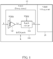
- FIG. 1 is a diagram illustrating basic architecture of a proposed level converting enable latch according to an embodiment of the present invention.
- the level converting enable latch (labeled as "LCE_Latch”) 100 includes a level shifter circuit 102 and a latch circuit 104. It should be noted that the level converting enable latch 100 may include additional circuit components, depending upon actual design considerations.
- the level converting enable latch 100 receives a data input signal I from a logic circuit in a first power domain such as a power down domain 10 with a power supply voltage VDD1, and generates a data output signal Q to a logic circuit in a second power domain such as an always-on domain 20 with a power supply voltage VDD2.
- the level shifter circuit 102 is powered by the power supply voltage VDD2, and arranged to receive the data input signal I from the logic circuit in the power down domain 10, and generate the data output signal I LS according to the data input signal I.
- the level shifter circuit 102 is arranged to convert the voltage difference between the power supply voltages VDD1 and VDD2, such that the data input signal I of the level shifter circuit 102 has a voltage swing of (VDD1-VSS), and the data output signal I LS of the level shifter circuit 102 has a voltage swing of (VDD2-VSS), where VSS is a ground voltage.
- the latch circuit 104 is powered by the power supply voltage VDD2.
- the latch circuit 104 is arranged to receive the data output signal I LS from the level shifter circuit 102 and set the data output signal Q in response to the received data output signal I LS when a latch enable signal E is set by a first logic value, and is further arranged to latch the data output signal Q when the latch enable signal E is set by a second logic value that is different from the first logic value.
- the latch enable signal E is set by the first logic value
- the data output signal Q is allowed to vary with the data input signal I
- the latch enable signal E is set by the second logic value
- the data output signal Q holds a logic value that is obtained from the data input signal I at the time the latch enable signal E has a transition from the first logic value to the second value.
- the latch circuit 104 may have a latch feedback loop that can be selectively enabled or disabled under the control of the latch enable signal E.
- footer transistors of the level shifter circuit 102 may be reused to disable a cross-coupled function, where the footer transistors are originally implemented for electrostatic discharge (ESD) protection. Since the footer transistors of the level shifter circuit 102 are reused, the transistor count of the level converting enable latch 100 can be reduced, thereby making the level converting enable latch 100 have lower dynamic power.
- a quasi-inverter of the level shifter circuit 102 may be reused as a latch feedback inverter.
- the transistor count of the level converting enable latch 100 can be reduced, thereby making the level converting enable latch 100 have lower dynamic power.
- the quasi-inverter of the level shifter circuit 102 is reused as a latch feedback inverter located at a leakage path between VDD2 and VSS, the latch leakage power under a VDD1 power down scenario can be reduced. Further details of the proposed level converting enable latch 100 are described with reference to the accompanying drawings.
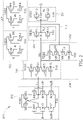
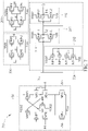
- FIG. 2 is a circuit diagram of a first level converting enable latch design according to an embodiment of the present invention.
- the level converting enable latch 200 follows the architecture shown in FIG. 1 , and includes a level shifter circuit 202 and a latch circuit 204.
- the level converting enable latch 200 may further include signal generation circuits 206 and 208 that act as buffers for providing cleaner data input signal(s) and cleaner latch enable signal(s).
- the signal generation circuit 206 operates according to different reference voltages including a power supply voltage VDD1 and a ground voltage VSS, and has a plurality of P-channel metal-oxide semiconductor (PMOS) transistors MP1, MP2 and a plurality of N-channel metal-oxide semiconductor (NMOS) transistors MN1, MN2.
- PMOS P-channel metal-oxide semiconductor
- NMOS N-channel metal-oxide semiconductor
- the signal generation circuit 206 includes one inverter consisting of PMOS transistor MP1 and NMOS transistor MN1, and another inverter consisting of PMOS transistor MP2 and NMOS transistor MN2.
- the signal generation circuit 206 may be modified to omit PMOS transistor MP2 and NMOS transistor MN2, such that the data input signal I and an inverse of the data input signal I (i.e., data input signal ib) may be used by the level shifter circuit 202.
- the signal generation circuit 208 operates according to different reference voltages including a power supply voltage VDD2 (VDD2 ⁇ VDD1) of another power domain (e.g., always-on domain) and the ground voltage VSS, and has a plurality of PMOS transistors MP3, MP4 and a plurality of NMOS transistors MN3, MN4.
- the signal generation circuit 208 includes one inverter consisting of PMOS transistor MP3 and NMOS transistor MN3, and another inverter consisting of PMOS transistor MP4 and NMOS transistor MN4.
- the signal generation circuit 208 may be modified to omit PMOS transistor MP4 and NMOS transistor MN4, such that the latch enable signal E and an inverse of the latch enable signal (i.e., latch enable signal eb) may be used by the latch circuit 204.
- the level shifter circuit 202 is arranged to receive the data input signal ibb, and generate and output a data output signal I LS .
- the data output signal I LS may be regarded as a level-shifting version of an inverse of the data input signal ibb, that is, a level-shifting version of the data input signal ib.
- the data input signal ibb of the level shifter circuit 202 has a voltage swing of (VDD1-VSS), while the data output signal I LS of the level shifter circuit 202 has a voltage swing of (VDD2-VSS) .
- the level shifter circuit 202 employs cross-coupled level shifter architecture, and therefore can support both VDD1 > VDD2 and VDD1 ⁇ VDD2.
- the level shifter circuit 202 includes PMOS transistors MP5, MP6, MP7, MP8 and NMOS transistors MN5, MN6, and further includes optional NMOS transistors MN7, MN8 that act as footer transistors for ESD protection.
- Each of PMOS transistors and NMOS transistors has a control terminal (e.g., gate terminal) and two connection terminals (e.g., source terminal and drain terminal).
- the PMOS transistor MP5 has a source terminal coupled to the power supply voltage VDD2, a drain terminal coupled to a source terminal of the PMOS transistor MP7, and a gate terminal coupled to a drain terminal of the NMOS transistor MN6; and the PMOS transistor MP6 has a source terminal coupled to the power supply voltage VDD2, a drain terminal coupled to a source terminal of the PMOS transistor MP8, and a gate terminal coupled to a drain terminal of the NMOS transistor MN5.
- the PMOS transistor MP7 has a drain terminal coupled to the drain terminal of the NMOS transistor MN5 and a gate terminal coupled to a gate terminal of the NMOS transistor MN5
- the PMOS transistor MP8 has a drain terminal coupled to the drain terminal of the NMOS transistor MN6 and a gate terminal coupled to a gate terminal of the NMOS transistor MN6
- a source terminal of the NMOS transistor MN5 is coupled to a source terminal of the NMOS transistor MN6.
- the NMOS transistors MN7 and MN8 act as footer transistors for ESD protection.
- the NMOS transistor MN7 has a drain terminal coupled to the source terminal of the NMOS transistor MN5, a source terminal coupled to the ground voltage VSS, and a gate terminal arranged to receive a high bias voltage tieH, where the NMOS transistor MN7 is turned on by the high bias voltage tieH under a normal mode.
- the NMOS transistor MN8 has a drain terminal coupled to the source terminal of the NMOS transistor MN6, a source terminal coupled to the ground voltage VSS, and a gate terminal arranged to receive the high bias voltage tieH, where the NMOS transistor MN8 is turned on by the high bias voltage tieH under a normal mode.
- FIG. 2 is a diagram illustrating an alternative design of the level shifter circuit 202 used by the level converting enable latch 200 shown in FIG. 2 according to an embodiment of the present invention.
- the level shifter circuit 202 shown in FIG. 2 may be replaced with the level shifter circuit 300 shown in FIG. 3 .
- the major difference between the level shifter circuits 202 and 300 is that the level shifter circuit 300 does not have PMOS transistors MP7 and MP8 included in the level shifter circuit 202.
- the NMOS transistors MN7 and MN8 act as footer transistors for ESD protection.
- the level shifter circuit 202/300 may be modified to omit the NMOS transistors MN7 and MN8 and directly connect source terminals of the NMOS transistors MN5 and MN6 to the ground voltage VSS.
- the data output signal I LS is a level-shifting version of an inverse of the data input signal ibb.
- the latch circuit 204 is arranged to receive the data output signal I LS and set the data output signal Q in response to the data output signal I LS when the latch enable signal E is set by one logic value 1, and latch the data output signal Q when the latch enable signal E is set by another logic value 0.
- the power supply voltage VDD1 may be shut down for power saving.
- the latch circuit 204 includes a plurality of control circuits 210, 212 and a plurality of inverters 214, 216.
- the control circuit 210 includes a plurality of PMOS transistors MP9, MP10 and a plurality of NMOS transistors MN9, MN10.
- the PMOS transistor MP9 has a source terminal coupled to the power supply voltage VDD2, a gate terminal arranged to receive the data output signal I LS , and a drain terminal coupled to a source terminal of the PMOS transistor MP10.
- the PMOS transistor MP10 has a gate terminal arranged to receive the latch enable signal eb and a drain terminal coupled to a drain terminal of the NMOS transistor MN9.
- the NMOS transistor MN9 has a gate terminal arranged to receive the latch enable signal ebb and a source terminal coupled to a drain terminal of the NMOS transistor MN10.
- the NMOS transistor MN10 has a gate terminal arranged to receive the data output signal I LS and a source terminal coupled to the ground voltage VSS.
- the control circuit 210 has PMOS transistor MP10 and NMOS transistor MN9 both being turned on, and has an inverter (which consists of PMOS transistor MP9 and NMOS transistor MN9) that is active to invert the data output signal I LS to generate a data output signal IB LS at drain terminals of PMOS transistor MP10 and NMOS transistor MN9, where the data output signal IB LS is an inverse of the data output signal I LS .
- the latch enable signal E is set by the logic value 1
- the control circuit 210 allows the data output signal IB LS to be derived from the data output signal I LS .
- the latch enable signal E When the latch enable signal E is set by the logic value 0, the latch enable signal eb has the logic value 1, and the latch enable signal ebb has the logic value 0. Hence, the control circuit 210 is disabled due to PMOS transistor MP10 and NMOS transistor MN9 both being turned off. In other words, when the latch enable signal E is set by the logic value 0, the control circuit 210 blocks the data output signal IB LS from being derived from the data output signal I L .
- the data output signal Q is set in response to the data output signal IB LS through inverters 214 and 216.
- the inverters 214 consists of PMOS transistor MP11 and NMOS transistor MN11, and has an input node N1 arranged to receive the data output signal IB LS .
- the inverter 216 consists of PMOS transistor MP12 and NMOS transistor MN12, and has an input node N3 coupled to an output node N2 of the inverter 214 and an output node N4 arranged to output the data output signal Q.
- the control circuit 212 includes a plurality of PMOS transistors MP13, MP14 and a plurality of NMOS transistors MN13, MN14.
- the PMOS transistor MP13 has a source terminal coupled to the power supply voltage VDD2, a gate terminal coupled to the output node N2 of the inverter 214, and a drain terminal coupled to a source terminal of the PMOS transistor MP14.
- the PMOS transistor MP14 has a gate terminal arranged to receive the latch enable signal ebb, and a drain terminal coupled to a drain terminal of the NMOS transistor MN13.
- the NMOS transistor MN13 has a gate terminal arranged to receive the latch enable signal eb, and a source terminal coupled to a drain terminal of the NMOS transistor MN14.
- the NMOS transistor MN14 has a gate terminal coupled to the output node N2 of the inverter 214, and a source terminal coupled to the ground voltage VSS.
- the latch enable signal E When the latch enable signal E is set by the logic value 0, the latch enable signal eb has the logic value 1, and the latch enable signal ebb has the logic value 0. Hence, the control circuit 212 disables a latch feedback loop 215 due to PMOS transistor MP14 and NMOS transistor MN13 both being turned off.
- the latch enable signal E When the latch enable signal E is set by the logic value 1, the latch enable signal eb has the logic value 0, and the latch enable signal ebb has the logic value 1.
- control circuit 212 enables the latch feedback loop 215 due to PMOS transistor MP14 and NMOS transistor MN13 both being turned on, and also has an inverter (which consists of PMOS transistor MP13 and NMOS transistor MN14) that is active for inverting an output signal of the inverter 214 to set an input signal (i.e., data output signal IB LS ) of the inverter 214.
- an inverter which consists of PMOS transistor MP13 and NMOS transistor MN14
- the latch circuit 204 is a high-enable type latch.
- the latch feedback loop 215 is cut off and the control circuit 210 sets an input signal of the inverter 214 by inverting the data output signal I LS (which is an output of the level shifter circuit 202), such that the data output signal Q is set in response to the data output signal I LS through the control circuit 210 and the inverters 214 and 216.
- control circuit 210 blocks an input signal of the inverter 214 from being affected by the level shifter circuit 202, and the latch feedback loop 215 is enabled, such that the data output signal Q is latched through the control circuit 212 and the inverters 214 and 216.
- FIG. 4 is a diagram illustrating an operation scenario of a high-enable type latch according to an embodiment of the present invention.
- the latch enable signal E is set by the logic value 1
- the data output signal Q is set in response to the data input signal I.
- the latch enable signal E is set by the logic value 1
- the data output signal Q is latched, regardless of the data input signal I. Since the data output signal Q is latched, the power supply VDD1 of the power down domain can be shut down for power saving.
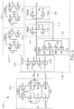
- FIG. 5 is a circuit diagram of a second level converting enable latch design according to an embodiment of the present invention.
- the level converting enable latch 500 follows the architecture shown in FIG. 1 .
- the major difference between the level converting enable latches 500 and 200 is that a PMOS transistor MP10 of a control circuit 510 in a latch circuit 504 has a gate terminal arranged to receive the latch enable signal ebb, an NMOS transistor MN9 of the control circuit 510 in the latch circuit 504 has a gate terminal arranged to receive the latch enable signal eb, a PMOS transistor MP14 of a control circuit 512 in the latch circuit 504 has a gate terminal arranged to receive the latch enable signal eb, and an NMOS transistor MN13 of the control circuit 512 in the latch circuit 504 has a gate terminal arranged to receive the latch enable signal ebb.
- the latch circuit 504 is a low-enable type latch.
- control circuit 510 blocks an input signal of the inverter 214 from being affected by the level shifter circuit 202, and the latch feedback loop 215 is enabled, such that the data output signal Q is latched through the control circuit 512 and the inverters 214 and 216.
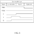
- FIG. 6 is a diagram illustrating an operation scenario of a low-enable type latch according to an embodiment of the present invention.
- the latch enable signal E is set by the logic value 0
- the data output signal Q is set in response to the data input signal I.
- the latch enable signal E is set by the logic value 1
- the data output signal Q is latched, regardless of the data input signal I. Since the data output signal Q is latched, the power supply VDD1 of the power down domain can be shut down for power saving.
- FIG. 7 is a circuit diagram of a third level converting enable latch design according to an embodiment of the present invention.
- the level converting enable latch 700 follows the architecture shown in FIG. 1 , and includes a level shifter circuit 702 and a latch circuit 704.
- the level converting enable latch 700 may further include the aforementioned signal generation circuits 206 and 208 that act as buffers for providing cleaner data input signal (s) and cleaner latch enable signal(s).
- this is not meant to be a limitation of the present invention.
- the signal generation circuit 206 may be modified to omit PMOS transistor MP2 and NMOS transistor MN2, such that the data input signal I and an inverse of the data input signal I (i.e., data input signal ib) may be used by the level shifter circuit 702.
- the signal generation circuit 208 may be modified to omit PMOS transistor MP4 and NMOS transistor MN4, such that the latch enable signal E and an inverse of the latch enable signal (i.e., latch enable signal eb) may be used by the latch circuit 704, and the latch enable signal E may be used by the level shifter circuit 702.
- the level shifter circuit 702 is arranged to receive the data input signal ibb, and generate and output the data output signal I LS .
- the data output signal I LS may be regarded as a level-shifting version of the data input signal ibb.
- the data input signal ibb of the level shifter circuit 702 has a voltage swing of (VDD1-VSS), while the data output signal I LS of the level shifter circuit 702 has a voltage swing of (VDD2-VSS).
- the level shifter circuit 702 employs cross-coupled level shifter architecture, and therefore can support both VDD1 > VDD2 and VDD1 ⁇ VDD2. As shown in FIG.
- the level shifter circuit 702 includes PMOS transistors MP5, MP6, MP7, MP8, MP15, and NMOS transistors MN5, MN6, MN7, MN8, where the NMOS transistors MN7 and MN8 can act as footer transistors for ESD protection.
- the major difference between the level shifter circuits 702 and 202 is that the data input signal ibb is received by gate terminals of PMOS transistor MP7 and NMOS transistor MN5, the data input signal ib is received by gate terminals of PMOS transistor MP8 and NMOS transistor MN6, the latch enable signal ebb is received by gate terminals of NMOS transistors MN7, MN8, and the additional PMOS transistor MP15 has a source terminal coupled to the power supply voltage VDD2, a drain terminal coupled to the drain terminal of the NMOS transistor MN5, and a gate terminal arranged to receive the latch enable signal ebb.
- the latch enable signal ebb When the latch enable signal E is set by the logic value 1, the latch enable signal ebb has the logic value 1. Hence, the PMOS transistor MP15 is turned off and the NMOS transistors MN7 and MN8 are turned on, thus allowing the level shifter circuit 702 to work normally for applying level-shifting to the data input signal ibb to set the data output signal I LS . However, when the latch enable signal E is set by the logic value 0, the latch enable signal ebb has the logic value 0. Hence, the NMOS transistors MN7 and MN8 are turned off, thus disabling a designated level-shifting function of the level shifter circuit 702.
- the PMOS transistor MP15 is turned on for coupling the power supply voltage VDD2 to one cross-coupled path.
- the PMOS transistor MP15 is controlled by the latch enable signal ebb for leakage reduction.
- the NMOS transistors MN7 and MN8 (which originally act as footer transistors for ESD protection) can be reused to take the place of the control circuit 210 shown in FIG. 2 .
- the latch circuit 704 may be obtained by removing the control circuit 210 from the latch circuit 204, such that the data output signal I LS output from the level shifter circuit 702 is received by the input node N1 of the inverter 214 when the latch feedback loop 215 is disabled by the control circuit 212, and is set by inverting an output signal of the inverter 214 when the latch feedback loop 215 is enabled by the control circuit 212.
- the latch enable signal E when the latch enable signal E is set by the logic value 1, the latch enable signal eb has the logic value 0, and the latch enable signal ebb has the logic value 1.
- the control circuit 212 disables the latch feedback loop 215 due to PMOS transistor MP14 and NMOS transistor MN13 both being turned off.
- the latch enable signal E is set by the logic value 0
- the latch enable signal eb has the logic value 1
- the latch enable signal ebb has the logic value 0.
- the control circuit 212 enables the latch feedback loop 215 due to PMOS transistor MP14 and NMOS transistor MN13 both being turned on, and has an inverter (which consists of PMOS transistor MP13 and NMOS transistor MN14) that is active for inverting the output signal of the inverter 214 to set an input signal (i.e., data output signal I LS ) of the inverter 214.
- an inverter which consists of PMOS transistor MP13 and NMOS transistor MN14
- FIG. 7 is for illustrative purposes only, and is not meant to be a limitation of the present invention.
- the level shifter circuit 702 may be modified to employ another cross-coupled level shifter architecture.
- FIG. 8 is a diagram illustrating an alternative design of the level shifter circuit 702 used by the level converting enable latch 700 shown in FIG. 7 according to an embodiment of the present invention.
- the level shifter circuit 702 shown in FIG. 7 may be replaced with the level shifter circuit 800 shown in FIG. 8 .
- the major difference between the level shifter circuits 702 and 800 is that the level shifter circuit 800 does not have the PMOS transistors MP7 and MP8 included in the level shifter circuit 702.
- the latch circuit 704 is a high-enable type latch.
- the footer transistors MN7 and MN8 are turned off to disable the cross-coupled function, and the latch feedback loop 215 is enabled, such that the data output signal Q is latched through the control circuit 212 and the inverters 214 and 216.
- the data output signal Q is set in response to the data input signal I; and during a period in which the latch enable signal E is set by the logic value 0, the data output signal Q is latched, regardless of the data input signal I. Since the data output signal Q is latched, the power supply VDD1 of the power down domain can be shut down for power saving.
- FIG. 9 is a circuit diagram of a fourth level converting enable latch design according to an embodiment of the present invention.
- the level converting enable latch 900 follows the architecture shown in FIG. 1 .
- the major difference between the level converting enable latches 900 and 700 is that the latch enable signal eb is received by gate terminals of NMOS transistors MN7 and MN8 and PMOS transistor MP15 in a level shifter circuit 902, a PMOS transistor MP14 of the control circuit 512 used by a latch circuit 904 has a gate terminal arranged to receive the latch enable signal eb, and an NMOS transistor MN13 of the control circuit 512 used by the latch circuit 904 has a gate terminal arranged to receive the latch enable signal ebb.
- FIG. 9 is a diagram illustrating an alternative design of the level shifter circuit 902 in the level converting enable latch 900 shown in FIG. 9 according to an embodiment of the present invention.
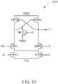
- the level shifter circuit 902 shown in FIG. 9 may be replaced with the level shifter circuit 1000 shown in FIG. 10 .
- the major difference between the level shifter circuits 902 and 1000 is that the level shifter circuit 1000 does not have the PMOS transistors MP7 and MP8 included in the level shifter circuit 902.
- the latch circuit 904 is a low-enable type latch.
- the data output signal Q is set in response to the data input signal I; and during a period in which the latch enable signal E is set by the logic value 1, the data output signal Q is latched, regardless of the data input signal I. Since the data output signal Q is latched, the power supply VDD1 of the power down domain can be shut down for power saving.
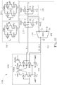
- FIG. 11 is a circuit diagram of a fifth level converting enable latch design according to an embodiment of the present invention.
- the level converting enable latch 1100 follows the architecture shown in FIG. 1 , and includes a level shifter circuit 1102 and a latch circuit 1104.
- the level converting enable latch 1100 may further include the aforementioned signal generation circuits 206 and 208 that act as buffers for providing cleaner data input signal (s) and cleaner latch enable signal (s) .
- this is not meant to be a limitation of the present invention.
- the signal generation circuit 206 may be modified to omit PMOS transistor MP2 and NMOS transistor MN2, such that the data input signal I and an inverse of the data input signal I (i.e., data input signal ib) may be used by the level shifter circuit 1102 and the latch circuit 1104.
- the signal generation circuit 208 may be omitted, such that the latch enable signal E may be directly used by the level shifter circuit 1102 and the latch circuit 1104.
- the level shifter circuit 1102 is arranged to receive the data input signal ibb, and generate and output the data output signal I LS .
- the data output signal I LS may be regarded as a level-shifting version of the data input signal ibb.
- the data input signal ibb of the level shifter circuit 1102 has a voltage swing of (VDD1-VSS), while the data output signal I LS of the level shifter circuit 1102 has a voltage swing of (VDD2-VSS) .
- the level shifter circuit 1102 employs cross-coupled level shifter architecture, and therefore can support both VDD1 > VDD2 and VDD1 ⁇ VDD2.
- the major difference between the level shifter circuits 1102 and 202 is that the data input signal ibb is received by gate terminals of PMOS transistor MP7 and NMOS transistor MN5, a multiplexer output M_OUT is received by gate terminals of PMOS transistor MP8 and NMOS transistor MN6, and an additional PMOS transistor MP16 has a source terminal coupled to the power supply voltage VDD2, a drain terminal coupled to the source terminal of the PMOS transistor MP8, and a gate terminal arranged to receive the latch enable signal ebb.
- the NMOS transistors MN7 and MN8 act as footer transistors for ESD protection.
- the level shifter circuit 1102 may be modified to omit the NMOS transistors MN7 and MN8 and directly couple source terminals of the NMOS transistors MN5 and MN6 to the ground voltage VSS.
- the latch circuit 1104 includes a multiplexer (MUX) 1106 and the aforementioned inverters 214 and 216.
- the multiplexer 1106 has one input node N5 coupled to the output node N2 of the inverter 214 and arranged to receive an internal signal preQ of the latch circuit 1104, another input node N6 arranged to receive the data input signal ib, and an output node N7 arranged to output the multiplexer output signal M OUT.
- the multiplexer 1106 is controlled by a selection signal that is set by the latch enable signal ebb. That is, the multiplexer 1106 refers to the latch enable signal ebb to select one of the internal signal preQ and the data input signal ib as the multiplexer output signal M OUT.
- the operation of the level shifter circuit 1102 is similar to that of the level shifter circuit 702, where the data output signal I LS may be regarded as a level-shifting version of the data input signal ibb, and the data output signal Q is set in response to the data output signal I LS through inverters 214 and 216.
- a quasi-inverter which consists of PMOS transistor MP8 and NMOS transistor MN6
- the latch circuit 1104 is a high-enable type latch.
- the data output signal Q is set in response to the data input signal I; and during a period in which the latch enable signal E is set by the logic value 0, the data output signal Q is latched, regardless of the data input signal I. Since the data output signal Q is latched, the power supply VDD1 of the power down domain can be shut down for power saving.
- FIG. 12 is a circuit diagram of a sixth level converting enable latch design according to an embodiment of the present invention.
- the level converting enable latch 1200 follows the architecture shown in FIG. 1 .
- the major difference between the level converting enable latches 1200 and 1100 is that, a PMOS transistor MP16 of a level shifter circuit 1202 has a gate terminal arranged to receive the latch enable signal eb, and a multiplexer 1206 of a latch circuit 1204 is arranged to select the data input signal ib as the multiplexer output signal M OUT when the latch enable signal ebb is set by the logic value 0 and arranged to select the internal signal preQ of the latch circuit 1204 as the multiplexer output signal M OUT when the latch enable signal ebb is set by the logic value 1.
- the latch circuit 1204 is a low-enable type latch.
- the data output signal Q is set in response to the data input signal I; and during a period in which the latch enable signal E is set by the logic value 1, the data output signal Q is latched, regardless of the data input signal I. Since the data output signal Q is latched, the power supply VDD1 of the power down domain can be shut down for power saving.
- the present invention may also be defined by the following numbered clauses.
Landscapes
- Engineering & Computer Science (AREA)
- Computer Hardware Design (AREA)
- Physics & Mathematics (AREA)
- Computing Systems (AREA)
- General Engineering & Computer Science (AREA)
- Mathematical Physics (AREA)
- Logic Circuits (AREA)
- Measurement Of Current Or Voltage (AREA)
Applications Claiming Priority (2)
| Application Number | Priority Date | Filing Date | Title |
|---|---|---|---|
| US202063084616P | 2020-09-29 | 2020-09-29 | |
| US17/368,866 US11606093B2 (en) | 2020-09-29 | 2021-07-07 | Level converting enable latch |
Publications (2)
| Publication Number | Publication Date |
|---|---|
| EP3975425A2 true EP3975425A2 (de) | 2022-03-30 |
| EP3975425A3 EP3975425A3 (de) | 2022-06-08 |
Family
ID=77021081
Family Applications (1)
| Application Number | Title | Priority Date | Filing Date |
|---|---|---|---|
| EP21186808.8A Pending EP3975425A3 (de) | 2020-09-29 | 2021-07-20 | Zur pegelumwandlung befähigte klinke |
Country Status (4)
| Country | Link |
|---|---|
| US (1) | US11606093B2 (de) |
| EP (1) | EP3975425A3 (de) |
| CN (1) | CN114337610A (de) |
| TW (1) | TWI788988B (de) |
Families Citing this family (4)
| Publication number | Priority date | Publication date | Assignee | Title |
|---|---|---|---|---|
| JP2022073314A (ja) * | 2020-10-30 | 2022-05-17 | ソニーセミコンダクタソリューションズ株式会社 | コンバインドロジック回路 |
| US12244311B2 (en) * | 2022-01-28 | 2025-03-04 | Taiwan Semiconductor Manufacturing Company, Ltd. | Power loss regulation circuit |
| EP4325500B1 (de) * | 2022-07-05 | 2025-04-16 | Changxin Memory Technologies, Inc. | Struktur zur datenübertragung, verfahren zur datenübertragung und speicher |
| CN121098309B (zh) * | 2025-09-23 | 2026-05-12 | 苏州顺芯半导体有限公司 | 快速电平转换电路 |
Citations (1)
| Publication number | Priority date | Publication date | Assignee | Title |
|---|---|---|---|---|
| US20190319624A1 (en) * | 2018-04-13 | 2019-10-17 | Taiwan Semiconductor Manufacturing Company, Ltd. | Level shifter circuit and method of operating the same |
Family Cites Families (19)
| Publication number | Priority date | Publication date | Assignee | Title |
|---|---|---|---|---|
| EP0713292A3 (de) * | 1994-11-21 | 1997-10-01 | Motorola Inc | Rückgekoppelte Verriegelungsschaltung und deren Betriebsverfahren |
| JP3530422B2 (ja) * | 1999-06-16 | 2004-05-24 | Necエレクトロニクス株式会社 | ラッチ回路とレジスタ回路 |
| KR100343290B1 (ko) * | 2000-03-21 | 2002-07-15 | 윤종용 | 반도체 메모리 장치의 입출력 감지 증폭기 회로 |
| US6563357B1 (en) | 2001-12-20 | 2003-05-13 | Intel Corporation | Level converting latch |
| AU2003277555A1 (en) | 2002-11-06 | 2004-06-07 | Nec Corporation | Level conversion circuit |
| KR100604904B1 (ko) * | 2004-10-02 | 2006-07-28 | 삼성전자주식회사 | 스캔 입력을 갖는 플립 플롭 회로 |
| US7956642B2 (en) | 2007-06-26 | 2011-06-07 | Qualcomm Incorporated | Level shifter having low duty cycle distortion |
| US7391250B1 (en) * | 2007-09-02 | 2008-06-24 | United Microelectronics Corp. | Data retention cell and data retention method based on clock-gating and feedback mechanism |
| US8587359B2 (en) | 2009-08-07 | 2013-11-19 | Atmel Corporation | Level shifter with output latch |
| CN202750074U (zh) * | 2012-04-20 | 2013-02-20 | 西安华迅微电子有限公司 | 一种高速比较器 |
| US8860487B2 (en) | 2012-11-29 | 2014-10-14 | Infineon Technologies Austria Ag | System and method for a level shifter |
| CN103856206A (zh) * | 2012-12-06 | 2014-06-11 | 上海华虹集成电路有限责任公司 | 从低到高逻辑电平转换电路 |
| US8994402B2 (en) | 2013-01-31 | 2015-03-31 | Oracle International Corporation | Level shifter circuit optimized for metastability resolution and integrated level shifter and metastability resolution circuit |
| CN103532526B (zh) | 2013-10-22 | 2016-05-18 | 北京兆易创新科技股份有限公司 | 电压转换电路及电压转换方法 |
| CN104796132B (zh) * | 2014-01-22 | 2017-12-22 | 陈祺琦 | 一种触发器电路 |
| US9941867B1 (en) * | 2016-09-20 | 2018-04-10 | Altera Corporation | Circuit and method for universal pulse latch |
| CN108322210A (zh) * | 2017-01-16 | 2018-07-24 | 中芯国际集成电路制造(上海)有限公司 | 一种电平转换电路 |
| US10340897B2 (en) * | 2017-07-28 | 2019-07-02 | Taiwan Semiconductor Manufacturing Company, Ltd. | Clock generating circuit and method of operating the same |
| US10651832B2 (en) * | 2018-08-10 | 2020-05-12 | Taiwan Semiconductor Manufacturing Company, Ltd. | Level shifter |
-
2021
- 2021-07-07 US US17/368,866 patent/US11606093B2/en active Active
- 2021-07-20 EP EP21186808.8A patent/EP3975425A3/de active Pending
- 2021-09-01 TW TW110132413A patent/TWI788988B/zh active
- 2021-09-22 CN CN202111107220.0A patent/CN114337610A/zh active Pending
Patent Citations (2)
| Publication number | Priority date | Publication date | Assignee | Title |
|---|---|---|---|---|
| US20190319624A1 (en) * | 2018-04-13 | 2019-10-17 | Taiwan Semiconductor Manufacturing Company, Ltd. | Level shifter circuit and method of operating the same |
| CN110380722A (zh) * | 2018-04-13 | 2019-10-25 | 台湾积体电路制造股份有限公司 | 集成电路 |
Also Published As
| Publication number | Publication date |
|---|---|
| US11606093B2 (en) | 2023-03-14 |
| TWI788988B (zh) | 2023-01-01 |
| EP3975425A3 (de) | 2022-06-08 |
| TW202213946A (zh) | 2022-04-01 |
| US20220103175A1 (en) | 2022-03-31 |
| CN114337610A (zh) | 2022-04-12 |
Similar Documents
| Publication | Publication Date | Title |
|---|---|---|
| US5736869A (en) | Output driver with level shifting and voltage protection | |
| TWI788988B (zh) | 電平轉換使能鎖存器 | |
| KR0120565B1 (ko) | 래치-업을 방지한 씨모스형 데이타 출력버퍼 | |
| US6433586B2 (en) | Semiconductor logic circuit device of low current consumption | |
| US7622954B2 (en) | Level shifter with memory interfacing two supply domains | |
| TWI737299B (zh) | 緩衝電路與緩衝方法 | |
| TW200522082A (en) | Power-up circuit in semiconductor memory device | |
| US7908499B2 (en) | Semiconductor integrated circuit comprising master-slave flip-flop and combinational circuit with pseudo-power supply lines | |
| EP1601102A1 (de) | Hochgeschwindigkeits-Flipflopschaltung | |
| KR100363381B1 (ko) | 반도체 칩, 반도체 인터페이스 회로, 반도체 칩의 회로보호 방법 및 그 보호 회로 | |
| US6566932B2 (en) | On-chip system with voltage level converting device for preventing leakage current due to voltage level difference | |
| US7382168B2 (en) | Buffer circuit with multiple voltage range | |
| JP5643158B2 (ja) | レベルシフト回路 | |
| US6201428B1 (en) | 5-volt tolerant 3-volt drive push-pull buffer/driver | |
| KR100223744B1 (ko) | 혼합 전압 입력 버퍼 | |
| US6191636B1 (en) | Input buffer/level shifter | |
| JP5255244B2 (ja) | 入出力装置 | |
| JP2002185307A (ja) | 中継用マクロセル | |
| KR100610009B1 (ko) | 저전력 소모를 위한 반도체 장치 | |
| KR20190085305A (ko) | 입출력 회로 및 이를 포함하는 전자 소자 | |
| KR20070009255A (ko) | 반도체 장치의 전원공급 회로 및 전원공급 방법 | |
| KR20020084446A (ko) | 전압 인터페이스 회로를 구비한 반도체 집적 회로 장치 | |
| JP5266974B2 (ja) | 入出力回路 | |
| CN108242921A (zh) | 锁存器和分频器 | |
| TWI797947B (zh) | 電源管理電路、系統上晶片裝置及電源管理方法 |
Legal Events
| Date | Code | Title | Description |
|---|---|---|---|
| PUAI | Public reference made under article 153(3) epc to a published international application that has entered the european phase |
Free format text: ORIGINAL CODE: 0009012 |
|
| STAA | Information on the status of an ep patent application or granted ep patent |
Free format text: STATUS: THE APPLICATION HAS BEEN PUBLISHED |
|
| AK | Designated contracting states |
Kind code of ref document: A2 Designated state(s): AL AT BE BG CH CY CZ DE DK EE ES FI FR GB GR HR HU IE IS IT LI LT LU LV MC MK MT NL NO PL PT RO RS SE SI SK SM TR |
|
| PUAL | Search report despatched |
Free format text: ORIGINAL CODE: 0009013 |
|
| AK | Designated contracting states |
Kind code of ref document: A3 Designated state(s): AL AT BE BG CH CY CZ DE DK EE ES FI FR GB GR HR HU IE IS IT LI LT LU LV MC MK MT NL NO PL PT RO RS SE SI SK SM TR |
|
| RIC1 | Information provided on ipc code assigned before grant |
Ipc: H03K 3/356 20060101AFI20220503BHEP |
|
| STAA | Information on the status of an ep patent application or granted ep patent |
Free format text: STATUS: REQUEST FOR EXAMINATION WAS MADE |
|
| 17P | Request for examination filed |
Effective date: 20221205 |
|
| RBV | Designated contracting states (corrected) |
Designated state(s): AL AT BE BG CH CY CZ DE DK EE ES FI FR GB GR HR HU IE IS IT LI LT LU LV MC MK MT NL NO PL PT RO RS SE SI SK SM TR |
|
| P01 | Opt-out of the competence of the unified patent court (upc) registered |
Effective date: 20230607 |
|
| STAA | Information on the status of an ep patent application or granted ep patent |
Free format text: STATUS: EXAMINATION IS IN PROGRESS |
|
| 17Q | First examination report despatched |
Effective date: 20250401 |