EP3971966A1 - Wortleitungsstruktur und herstellungsverfahren dafür und halbleiterspeicher - Google Patents
Wortleitungsstruktur und herstellungsverfahren dafür und halbleiterspeicher Download PDFInfo
- Publication number
- EP3971966A1 EP3971966A1 EP21774339.2A EP21774339A EP3971966A1 EP 3971966 A1 EP3971966 A1 EP 3971966A1 EP 21774339 A EP21774339 A EP 21774339A EP 3971966 A1 EP3971966 A1 EP 3971966A1
- Authority
- EP
- European Patent Office
- Prior art keywords
- word line
- line contact
- word
- word lines
- substrate
- Prior art date
- Legal status (The legal status is an assumption and is not a legal conclusion. Google has not performed a legal analysis and makes no representation as to the accuracy of the status listed.)
- Ceased
Links
Images



Classifications
-
- H—ELECTRICITY
- H10—SEMICONDUCTOR DEVICES; ELECTRIC SOLID-STATE DEVICES NOT OTHERWISE PROVIDED FOR
- H10B—ELECTRONIC MEMORY DEVICES
- H10B12/00—Dynamic random access memory [DRAM] devices
- H10B12/30—DRAM devices comprising one-transistor - one-capacitor [1T-1C] memory cells
-
- G—PHYSICS
- G11—INFORMATION STORAGE
- G11C—STATIC STORES
- G11C8/00—Arrangements for selecting an address in a digital store
- G11C8/14—Word line organisation; Word line lay-out
-
- H—ELECTRICITY
- H10—SEMICONDUCTOR DEVICES; ELECTRIC SOLID-STATE DEVICES NOT OTHERWISE PROVIDED FOR
- H10B—ELECTRONIC MEMORY DEVICES
- H10B12/00—Dynamic random access memory [DRAM] devices
- H10B12/30—DRAM devices comprising one-transistor - one-capacitor [1T-1C] memory cells
- H10B12/48—Data lines or contacts therefor
- H10B12/488—Word lines
-
- H—ELECTRICITY
- H10—SEMICONDUCTOR DEVICES; ELECTRIC SOLID-STATE DEVICES NOT OTHERWISE PROVIDED FOR
- H10W—GENERIC PACKAGES, INTERCONNECTIONS, CONNECTORS OR OTHER CONSTRUCTIONAL DETAILS OF DEVICES COVERED BY CLASS H10
- H10W70/00—Package substrates; Interposers; Redistribution layers [RDL]
- H10W70/60—Insulating or insulated package substrates; Interposers; Redistribution layers
-
- H—ELECTRICITY
- H10—SEMICONDUCTOR DEVICES; ELECTRIC SOLID-STATE DEVICES NOT OTHERWISE PROVIDED FOR
- H10W—GENERIC PACKAGES, INTERCONNECTIONS, CONNECTORS OR OTHER CONSTRUCTIONAL DETAILS OF DEVICES COVERED BY CLASS H10
- H10W70/00—Package substrates; Interposers; Redistribution layers [RDL]
- H10W70/60—Insulating or insulated package substrates; Interposers; Redistribution layers
- H10W70/611—Insulating or insulated package substrates; Interposers; Redistribution layers for connecting multiple chips together
-
- H—ELECTRICITY
- H10—SEMICONDUCTOR DEVICES; ELECTRIC SOLID-STATE DEVICES NOT OTHERWISE PROVIDED FOR
- H10W—GENERIC PACKAGES, INTERCONNECTIONS, CONNECTORS OR OTHER CONSTRUCTIONAL DETAILS OF DEVICES COVERED BY CLASS H10
- H10W70/00—Package substrates; Interposers; Redistribution layers [RDL]
- H10W70/60—Insulating or insulated package substrates; Interposers; Redistribution layers
- H10W70/62—Insulating or insulated package substrates; Interposers; Redistribution layers characterised by their interconnections
- H10W70/65—Shapes or dispositions of interconnections
-
- G—PHYSICS
- G11—INFORMATION STORAGE
- G11C—STATIC STORES
- G11C11/00—Digital stores characterised by the use of particular electric or magnetic storage elements; Storage elements therefor
- G11C11/21—Digital stores characterised by the use of particular electric or magnetic storage elements; Storage elements therefor using electric elements
- G11C11/34—Digital stores characterised by the use of particular electric or magnetic storage elements; Storage elements therefor using electric elements using semiconductor devices
- G11C11/40—Digital stores characterised by the use of particular electric or magnetic storage elements; Storage elements therefor using electric elements using semiconductor devices using transistors
- G11C11/401—Digital stores characterised by the use of particular electric or magnetic storage elements; Storage elements therefor using electric elements using semiconductor devices using transistors forming cells needing refreshing or charge regeneration, i.e. dynamic cells
- G11C11/4063—Auxiliary circuits, e.g. for addressing, decoding, driving, writing, sensing or timing
- G11C11/407—Auxiliary circuits, e.g. for addressing, decoding, driving, writing, sensing or timing for memory cells of the field-effect type
- G11C11/408—Address circuits
Definitions
- the application relates to a word line structure, a manufacturing method thereof, and a semiconductor memory.
- a semiconductor memory is a memory accessed by using a semiconductor circuit, where a Dynamic Random Access Memory (DRAM) is widely used in various fields with high storage speed and high integration level.
- DRAM Dynamic Random Access Memory
- a first aspect of this application provides a word line structure, which includes a first word line array and a second word line array.
- the first word line array includes a plurality of first word lines extending in an X direction.
- the plurality of first word lines have a same length and are aligned and arranged in a Y direction.
- the second word line array includes a plurality of second word lines extending in the X direction.
- the plurality of second word lines have a same length and are aligned and arranged in the Y direction.
- the first word line array and the second word line array are not aligned in the Y direction, and the Y direction is perpendicular to the X direction.
- a second aspect of this application provides a semiconductor memory, which includes: a word line structure as described above; and a memory cell.
- the memory cell includes a memory capacitor and a transistor.
- a gate of the transistor is connected to a word line, a drain of the transistor is connected to a bit line, and a source of the transistor is connected to the memory capacitor.
- a plurality of memory cells are arranged in an array consisting of M rows and N columns, the memory cells in a same row share one word line, the memory cells in a same column share one bit line, the word line has the word line structure, and both M and N are positive integers.
- a third aspect of this application provides a manufacturing method of a word line structure, which includes following operations.
- a substrate is provided, in which an isolation structure and an active region are formed in the substrate.
- a hard mask layer is formed on a surface of the substrate.
- the hard mask layer is patterned, in which the patterned hard mask layer has a pattern same as a pattern of word lines.
- the substrate is etched through the patterned hard mask layer to form word line trenches.
- the word line trenches are filled with a conductive material layer, and the conductive material layer is etched so that a top of the conductive material layer is lower than the surface of the substrate and the remaining conductive material layer serves as first word lines and second word lines.
- the word line trenches are filled with a dielectric layer, in which the dielectric layer has a top flush with the surface of the substrate.
- the dielectric layer and the substrate in a set region are etched to the first word line or the second word line to form word line contact grooves for forming first word line contact structures and second word line contact structures.
- a contact material layer is deposited in the first word line contact groove and the second word line contact groove and on the surface of the substrate, and the contact material layer on the surface of the substrate is removed, in which the remaining contact material layer serves as the first word line contact structures and the second word line contact structures.
- a DRAM includes a plurality of repeated memory cells. As the size of the DRAM is continuously reduced and the integration level is continuously improved, the feature size and the unit area of the DRAM are reduced. Therefore, the area of a word line contact structure is correspondingly reduced, so that the contact resistance between the word line contact structure and corresponding word line is increased, which causes current flowing through the word line too small, and therefore the turn-on and turn-off speed of a switch in the memory cell of the DRAM is improved.
- FIG. 1 is a schematic diagram of a word line contact structure according to an embodiment. As shown in FIG. 1 , a word line structure includes a first word line array 100 and a second word line array 200.
- the first word line array 100 includes a plurality of first word lines 110 extending in an X direction.
- the plurality of first word lines 110 have a same length and are aligned and arranged in a Y direction.
- the second word line array 200 includes a plurality of second word lines 210 extending in the X direction.
- the plurality of second word lines 210 have a same length and are aligned and arranged in the Y direction.
- the first word line array 100 and the second word line array 200 are not aligned in the Y direction.
- the Y direction is perpendicular to the X direction.
- first word line array 100 and the second word line array 200 are not aligned in the Y direction means that the first word line array 100 and the second word line array 200 are in different columns, i.e. a first axis of symmetry of the first word line array 100 extending in the Y direction does not coincide with a second axis of symmetry of the second word line array 200 extending in the Y direction.
- both the first word lines 110 and the second word lines 210 are formed on word line trenches.
- a plurality of active regions 300 are disposed in a substrate. Each active region 300 is used to form a memory cell. Projections of each first word line 110 and each second word line 210 on the substrate pass through multiple active regions 300.
- the first word lines 110 and the second word lines 210 are used to control the turn-on and turn-off of transistors of memory cells.
- the cross-section in the present embodiment refers to a section parallel to the surface of the substrate, the cross-section in the following embodiment has the same definition as that in the present embodiment, and descriptions thereof are omitted.
- the plurality of first word lines 110 are equidistantly arranged at a set interval in the Y direction.
- the plurality of second word lines 210 are equidistantly arranged at the set interval in the Y direction.
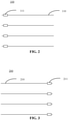
- FIG. 2 is a schematic diagram of a first word line array 100 according to the present embodiment.
- FIG. 3 is a schematic diagram of a second word line array 200 according to the present embodiment. As shown in FIGS. 2 and 3 , providing a plurality of equidistantly arranged first word lines 110 and a plurality of equidistantly arranged second word lines 210 allow the first word lines 110 and the second word lines 210 to be adapted to regularly -aligned active regions.
- the active regions connected to the first word lines 110 and the active regions connected to the second word lines 210 may be more compatibly arranged on the substrate, thereby reducing the design difficulty and the processing difficulty of the active regions, the first word lines 110, and the second word lines 210.
- the plurality of first word lines 110 and the plurality of second word lines 210 are spaced apart from each other in the Y direction. That is, two word lines adjacent to each first word line 110 are second word lines 210, and two word lines adjacent to each second word line 210 are first word lines 110.
- the present embodiment greatly improves the word line distribution density in the word line structure, thereby reducing the device area occupied by the word line structure in the Y direction, further improving the integration level of a semiconductor device, and reducing the area of the semiconductor device.
- the plurality of first word lines 110 have first word line contact structures 111 on a positive side of the X direction.
- the plurality of second word lines 210 have second word line contact structures 211 on a negative side of the X direction.
- the plurality of first word lines 110 have first word line contact structures 111 on a negative side of the X direction.
- the plurality of second word lines 210 have second word line contact structures 211 on a positive side of the X direction. It will be understood that if the first word line contact structure 111 and the second word line contact structure 211 are both disposed on a same side of the corresponding word lines, e.g. both disposed on the positive side in the X direction or the negative side in the X direction, the arrangement space of the word line contact structures will be very limited.
- the sizes of the first word line contact structure 111 and the second word line contact structure 211 in the Y direction may be 1.2 to 2 times a minimum process size.
- the first word line contact structure 111 and the second word line contact structure 211 have a same cross-sectional area.
- the contact resistance between each word line contact structure and the corresponding word line may be the same.
- current flowing through each word line is the same under the same condition, so that turn-on and turn-off speeds of a switch in each memory cell are consistent with each other, thereby avoiding the performance difference between different memory cells, and improving the reliability of overall performance of the device.
- the first word line contact structure 111 and the second word line contact structure 211 each have a rectangular, T-shaped, or semicircular cross-section.
- the first word line contact structure 111 and the second word line contact structure 211 in the embodiment of FIG. 1 are rectangular word line contact structures.
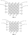
- FIG. 4 is a schematic diagram of a T-shaped word line contact structure according to an embodiment.
- FIG. 5 is a schematic diagram of a semicircular word line contact structure according to an embodiment.
- the first word line contact structure 111 and the second word line contact structure 211 of any cross-sectional shape are suitable for the word line structure. Therefore, the word line contact structures of other cross-sectional shapes not shown in the present embodiment are also within the protection scope of the present embodiment.
- FIG. 6 is a schematic diagram of a word line structure with staggered word line contact structures according to an embodiment.
- a plurality of first word line contact structures 111 are arranged in a staggered manner, thereby widening the arrangement space of the first word line contact structures 111 in the X direction, increasing the size of the first word line contact structures 111 in the X direction, enlarging the contact area between the first word line contact structure 111 and the corresponding first word line 110, and further reducing the contact resistance.
- a plurality of second word line contact structures 211 are also arranged in a staggered manner, thereby widening the arrangement space of the second word line contact structures 211 in the X direction, increasing the size of the second word line contact structures 211 in the X direction, and enlarging the contact area between the second word line contact structure 211 and the corresponding first word line 110.
- the staggered word line contact structures necessarily cause the word line structure to become larger in size in the X direction, thereby requiring a larger device area to be occupied. Therefore, it is needed to select the appropriate sizes of the first word line contact structure 111 and the second word line contact structure 211 in the X direction to achieve the balance between the contact resistance and the device size.
- FIG. 7 is a schematic diagram of adjacent word line contact structures having complementary shapes according to an embodiment.
- the first word line contact structures 111 are T-shaped, and adjacent T-shaped first word line contact structures 111 are arranged in opposite directions.
- a first word line contact structure 111 with a larger cross-sectional area may be achieved in the present embodiment by complementing the shapes of the adjacent T-shaped first word line contact structures 111 to each other.
- adjacent T-shaped second word line contact structures 211 in the present embodiment are also arranged in opposite directions.
- the present embodiment does not specifically define the shapes and arrangement directions of the first word line contact structure 111 and the second word line contact structure 211.
- Other technical solutions capable of realizing shape complementation of adjacent word line contact structures as shown in FIG. 8 are also within the protection scope of this application.
- an end of each of the first word line contact structure 111 and the second word line contact structure 211 is electrically connected with a gate of a transistor, while an another end is electrically connected with a drive circuit.
- the drive circuit is used to select word lines to access the memory cell.
- the first word line contact structure 111 and/or the second word line contact structure 211 are grooved contact structures.
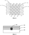
- FIG. 9 is a schematic diagram of a grooved contact structure according to the present embodiment.
- the grooved contact structure refers to a contact structure 430 formed by etching an interlayer dielectric layer 410, etching a word line 400 with a set depth to form a groove, and filling the groove with a conductive material.
- the word line 400 is electrically connected with a metal layer 420.
- the area of the word line contact structure can be reduced while a large contact area is ensured, and a contact and a short circuit between adjacent contact structures are prevented, so that the integration level and reliability of the semiconductor device are improved.
- a material of the first word line contact structure 111 and a material of the second word line contact structure 211 are one or more of tungsten, aluminum, copper, titanium, tantalum, or polysilicon. The above materials have good conductivity, thereby further reducing the contact resistance between the first word line contact structure 111 and the corresponding word line and the contact resistance between the second word line contact structure 211 and the corresponding word line.
- FIG. 10 shows a manufacturing method of a word line structure according to an embodiment. As shown in FIG. 10 , the manufacturing method of a word line structure includes steps S100 to S600.
- a substrate is provided, where an isolation structure and an active region are formed in the substrate.
- the substrate may be a silicon substrate or a germanium substrate.
- the isolation structure is formed in the substrate and used to define the active region in the substrate. After the isolation structure is formed, the active region is formed in the substrate by ion implantation.
- the isolation structure is a shallow-trench isolation structure.
- the step of forming the shallow-trench isolation structure is as follows. A trench is etched in the substrate. The trench is filled with a dielectric substance. A wafer surface is planarized by using a chemical mechanical polishing method.
- the trench is filled with a dielectric substance by adopting a chemical vapor deposition method and a material of the dielectric substance is such as silicon oxide.
- the shallow-trench isolation structure has a small surface area, is compatible with a chemical mechanical polishing technology, can be suitable for requirements of smaller line width and higher integration level, and is a better isolation technology. It needs be noted that the isolation structure in the present embodiment is not limited to the shallow-trench isolation structure, and other isolation structures capable of achieving isolation performance are also possible.
- a hard mask layer is formed on a surface of the substrate.
- a material of the hard mask layer may be at least one of silicon oxide, silicon nitride, silicon carbide, silicon oxynitride, silicon carbonitride, or silicon oxycarbonitride.
- the hard mask layer is used as a mask for etching of the substrate.
- the hard mask layer is patterned, in which the patterned hard mask layer has a pattern same as a pattern of word lines.
- the patterned hard mask layer is formed by adopting a Double-Patterning (DP) technology.
- the DP technology includes, but is not limited to, a Self-Aligned Double-Patterning (SADP) technology, a Litho-Etch-Litho-Etch (LELE) technology, and a Litho-Freeze-Litho (LFL) technology.
- SADP Self-Aligned Double-Patterning
- LELE Litho-Etch-Litho-Etch
- LFL Litho-Freeze-Litho
- the DP technology is adopted to improve the density of a word line trench and the integration level of a device.
- the substrate is etched through the patterned hard mask layer to form word line trenches.
- the word line trenches are filled with a conductive material layer, and the conductive material layer is etched so that a top of the conductive material layer is lower than the surface of the substrate and the remaining conductive material layer serves as first word lines 110 and second word lines 210.
- the plurality of first word lines 110 extend in an X direction.
- the plurality of first word lines 110 have a same length and are aligned and arranged in a Y direction.
- the plurality of second word lines 210 extend in the X direction.
- the plurality of second word lines 210 have a same length and are aligned and arranged in the Y direction.
- the first word line array 100 and the second word line array 200 are not aligned in the Y direction.
- the Y direction is perpendicular to the X direction.
- a material of the conductive material layer is one or more of tungsten, aluminum, titanium, tantalum, titanium nitride, or polysilicon.
- the word line trenches are filled with a dielectric layer, in which the dielectric layer has a top flush with the surface of the substrate; the substrate and the dielectric layer in a set region are etched to the first word line 110 or the second word line 210 to form word line contact grooves for forming first word line contact structures 111 and second word line contact structures 211; a contact material layer is deposited in the word line contact grooves and on the surface of the substrate; the contact material layer on the surface of the substrate is removed, and the remaining contact material layer serves as the first word line contact structures 111 and the second word line contact structures 211.
- steps in the flowchart of FIG. 10 are shown sequentially as indicated by the arrows, the steps are not necessarily performed sequentially as indicated by the arrows. Unless specifically stated otherwise herein, the steps are not performed in a strict order of limitation, and the steps may be performed in other orders. Moreover, at least a portion of the steps in FIG. 10 may include a plurality of sub-steps or stages that are not necessarily performed at the same time, but may be performed at different times, and the sub-steps or stages may be not necessarily performed sequentially, but may be performed in turn or alternately with at least a portion of other steps or the sub-steps or stages of other steps.
- a semiconductor memory which includes:
- a plurality of memory cells are arranged in an array consisting of M rows and N columns.
- the memory cells in a same row share one word line.
- the memory cells in a same column share one bit line.
- the word line has the word line structure. Both M and N are positive integers.
- the semiconductor memory of the present embodiment is based on the first word line array 100 and the second word line array 200 which are not aligned in the Y direction.
- the cross-sectional areas of the first word line contact structure 111 and the second word line contact structure 211 are enlarged by providing a larger arrangement space in a horizontal plane for the first word line contact structure 111 and the second word line contact structure 211. Therefore, the contact resistance between the first word line contact structure 111 and the corresponding word line and the contact resistance between the second word line contact structure 211 and the corresponding word line are reduced, and the turn-on and turn-off speed of a switch in the memory cell of the semiconductor memory is improved.
Landscapes
- Engineering & Computer Science (AREA)
- Microelectronics & Electronic Packaging (AREA)
- Semiconductor Memories (AREA)
Applications Claiming Priority (2)
| Application Number | Priority Date | Filing Date | Title |
|---|---|---|---|
| CN202010216024.6A CN113451269B (zh) | 2020-03-25 | 2020-03-25 | 字线结构和半导体存储器 |
| PCT/CN2021/079666 WO2021190294A1 (zh) | 2020-03-25 | 2021-03-09 | 字线结构及其制造方法、半导体存储器 |
Publications (2)
| Publication Number | Publication Date |
|---|---|
| EP3971966A1 true EP3971966A1 (de) | 2022-03-23 |
| EP3971966A4 EP3971966A4 (de) | 2022-12-07 |
Family
ID=77806647
Family Applications (1)
| Application Number | Title | Priority Date | Filing Date |
|---|---|---|---|
| EP21774339.2A Ceased EP3971966A4 (de) | 2020-03-25 | 2021-03-09 | Wortleitungsstruktur und herstellungsverfahren dafür und halbleiterspeicher |
Country Status (4)
| Country | Link |
|---|---|
| US (1) | US12453075B2 (de) |
| EP (1) | EP3971966A4 (de) |
| CN (1) | CN113451269B (de) |
| WO (1) | WO2021190294A1 (de) |
Families Citing this family (6)
| Publication number | Priority date | Publication date | Assignee | Title |
|---|---|---|---|---|
| CN116997179B (zh) * | 2022-04-24 | 2025-05-02 | 长鑫存储技术有限公司 | 半导体结构及其形成方法 |
| US12610538B2 (en) | 2022-04-24 | 2026-04-21 | Changxin Memory Technologies, Inc. | Semiconductor structure and method for forming semiconductor structure |
| CN115132778B (zh) * | 2022-07-06 | 2024-11-01 | 长江先进存储产业创新中心有限责任公司 | 相变存储器 |
| WO2024017077A1 (en) * | 2022-07-21 | 2024-01-25 | Yangtze Memory Technologies Co., Ltd. | Word-line-pickup structure and method for forming the same |
| WO2024188120A1 (zh) * | 2023-03-14 | 2024-09-19 | 长鑫科技集团股份有限公司 | 半导体结构及其制备方法 |
| CN118714844B (zh) * | 2023-03-16 | 2025-10-21 | 长鑫存储技术有限公司 | 半导体结构及其制备方法 |
Family Cites Families (31)
| Publication number | Priority date | Publication date | Assignee | Title |
|---|---|---|---|---|
| DE19811882A1 (de) * | 1998-03-18 | 1999-09-23 | Siemens Ag | DRAM-Zellenanordnung und Verfahren zu deren Herstellung |
| US6188095B1 (en) | 1998-09-30 | 2001-02-13 | Siemens Aktiengesellschaft | 6¼ f2 DRAM cell structure with four nodes per bitline-stud and two topological wordline levels |
| JP3633354B2 (ja) * | 1999-03-29 | 2005-03-30 | 株式会社日立製作所 | 半導体装置 |
| JP3866599B2 (ja) * | 2002-03-22 | 2007-01-10 | Necエレクトロニクス株式会社 | 半導体装置 |
| US7019353B2 (en) | 2002-07-26 | 2006-03-28 | Micron Technology, Inc. | Three dimensional flash cell |
| DE10261457B3 (de) * | 2002-12-31 | 2004-03-25 | Infineon Technologies Ag | Integrierte Schaltungsanordnung mit einem Transistorarray aus vertikalen FET-Auswahltransistoren |
| US6818515B1 (en) | 2003-06-23 | 2004-11-16 | Promos Technologies Inc. | Method for fabricating semiconductor device with loop line pattern structure |
| KR100604875B1 (ko) * | 2004-06-29 | 2006-07-31 | 삼성전자주식회사 | 스트랩 영역을 갖는 비휘발성 반도체 메모리 소자 및 그제조방법 |
| JP4498088B2 (ja) * | 2004-10-07 | 2010-07-07 | 株式会社東芝 | 半導体記憶装置およびその製造方法 |
| US7139184B2 (en) * | 2004-12-07 | 2006-11-21 | Infineon Technologies Ag | Memory cell array |
| US7359279B2 (en) * | 2005-03-31 | 2008-04-15 | Sandisk 3D Llc | Integrated circuit memory array configuration including decoding compatibility with partial implementation of multiple memory layers |
| KR100650735B1 (ko) * | 2005-05-26 | 2006-11-27 | 주식회사 하이닉스반도체 | 상변환 기억 소자 및 그의 제조방법 |
| US20070218627A1 (en) * | 2006-03-15 | 2007-09-20 | Ludovic Lattard | Device and a method and mask for forming a device |
| JP4504402B2 (ja) * | 2007-08-10 | 2010-07-14 | 株式会社東芝 | 不揮発性半導体記憶装置 |
| US8437192B2 (en) * | 2010-05-21 | 2013-05-07 | Macronix International Co., Ltd. | 3D two bit-per-cell NAND flash memory |
| US20130094273A1 (en) | 2010-04-06 | 2013-04-18 | Wei-Chih Chien | 3d memory and decoding technologies |
| US8674522B1 (en) * | 2012-10-11 | 2014-03-18 | Nanya Technology Corp. | Castle-like chop mask for forming staggered datalines for improved contact isolation and pattern thereof |
| TWI530953B (zh) * | 2012-11-15 | 2016-04-21 | 旺宏電子股份有限公司 | 三維記憶體及解碼技術 |
| US20160351573A1 (en) * | 2013-03-25 | 2016-12-01 | Hiroshi Yoshino | Semiconductor device and method for manufacturing the same |
| KR20160067618A (ko) * | 2014-12-04 | 2016-06-14 | 삼성전자주식회사 | 트랜지스터들을 포함하는 반도체 소자 |
| US9886996B2 (en) | 2015-10-19 | 2018-02-06 | Taiwan Semiconductor Manufacturing Co., Ltd. | SRAM cell for interleaved wordline scheme |
| US10991675B2 (en) | 2016-10-10 | 2021-04-27 | Monolithic 3D Inc. | 3D semiconductor device and structure |
| EP3523825A4 (de) * | 2016-10-10 | 2020-09-09 | Monolithic 3D Inc. | 3d-halbleiterbauelement und struktur damit |
| KR102721029B1 (ko) * | 2017-01-10 | 2024-10-25 | 삼성전자주식회사 | 반도체 장치 및 이의 제조 방법 |
| CN109698193B (zh) * | 2017-10-24 | 2024-02-09 | 长鑫存储技术有限公司 | 一种半导体存储器的阵列结构 |
| CN207938611U (zh) * | 2017-12-27 | 2018-10-02 | 睿力集成电路有限公司 | 半导体存储器件结构 |
| CN107994018B (zh) * | 2017-12-27 | 2024-03-29 | 长鑫存储技术有限公司 | 半导体存储器件结构及其制作方法 |
| KR102471722B1 (ko) * | 2018-01-03 | 2022-11-29 | 삼성전자주식회사 | 반도체 메모리 장치 |
| CN110391234A (zh) * | 2018-04-20 | 2019-10-29 | 长鑫存储技术有限公司 | 位线连接结构及其形成方法、存储器 |
| KR102640292B1 (ko) * | 2018-07-16 | 2024-02-22 | 삼성전자주식회사 | 반도체 메모리 장치, 반도체 구조물, 및 반도체 장치 |
| KR102712036B1 (ko) * | 2019-04-30 | 2024-10-02 | 삼성전자주식회사 | 반도체 메모리 소자 및 이의 제조 방법 |
-
2020
- 2020-03-25 CN CN202010216024.6A patent/CN113451269B/zh active Active
-
2021
- 2021-03-09 EP EP21774339.2A patent/EP3971966A4/de not_active Ceased
- 2021-03-09 WO PCT/CN2021/079666 patent/WO2021190294A1/zh not_active Ceased
- 2021-07-27 US US17/386,499 patent/US12453075B2/en active Active
Also Published As
| Publication number | Publication date |
|---|---|
| WO2021190294A1 (zh) | 2021-09-30 |
| US20210358916A1 (en) | 2021-11-18 |
| CN113451269B (zh) | 2022-07-22 |
| EP3971966A4 (de) | 2022-12-07 |
| CN113451269A (zh) | 2021-09-28 |
| US12453075B2 (en) | 2025-10-21 |
Similar Documents
| Publication | Publication Date | Title |
|---|---|---|
| US12453075B2 (en) | Word line structure, manufacturing method thereof and semiconductor memory | |
| US9070640B2 (en) | Method of forming fine patterns of semiconductor device | |
| US7952140B2 (en) | Methods of fabricating semiconductor devices having multiple channel transistors and semiconductor devices fabricated thereby | |
| CN101297392B (zh) | 经硅化物化的内嵌硅 | |
| CN114342065A (zh) | 电容器阵列、存储器单元阵列、形成电容器阵列的方法以及形成存储器单元阵列的方法 | |
| US8415738B2 (en) | Semiconductor memory device and manufacturing method thereof | |
| CN113471200B (zh) | 存储器及其形成方法 | |
| TWI802469B (zh) | 記憶體裝置及其形成方法 | |
| US20170256413A1 (en) | Semiconductor Devices Using Auxiliary Layers for Trimming Margin and Devices So Formed | |
| US12432908B2 (en) | Semiconductor structure and method for fabricating same | |
| US20100244257A1 (en) | Method of fabricating semiconductor device and the semiconductor device | |
| CN115188708A (zh) | 半导体器件及其形成方法 | |
| CN114005791A (zh) | 存储器件及其形成方法 | |
| CN115172370A (zh) | 半导体结构及其形成方法 | |
| US12150293B2 (en) | Bit line structure, manufacturing method thereof and semiconductor memory | |
| JP2012054453A (ja) | 半導体装置の製造方法 | |
| TW202401771A (zh) | 半導體結構及其形成方法、佈局結構 | |
| CN117316974A (zh) | 半导体结构及其制作方法、存储器 | |
| CN115915752A (zh) | 半导体结构及其制作方法 | |
| KR20230073947A (ko) | U-형 채널 액세스 트랜지스터 및 이를 형성하는 방법 | |
| US9917161B2 (en) | Semiconductor device and method of fabricating the same | |
| US20220029015A1 (en) | Apparatuses comprising vertical transistors having gate electrodes at least partially recessed within channel regions, and related methods and systems | |
| US6876014B2 (en) | Interconnection structure of a semiconductor device | |
| US20230413528A1 (en) | Semiconductor structure, method for manufacturing semiconductor structure, and memory | |
| US20230084851A1 (en) | Storage device and method for forming storage device |
Legal Events
| Date | Code | Title | Description |
|---|---|---|---|
| STAA | Information on the status of an ep patent application or granted ep patent |
Free format text: STATUS: THE INTERNATIONAL PUBLICATION HAS BEEN MADE |
|
| PUAI | Public reference made under article 153(3) epc to a published international application that has entered the european phase |
Free format text: ORIGINAL CODE: 0009012 |
|
| STAA | Information on the status of an ep patent application or granted ep patent |
Free format text: STATUS: REQUEST FOR EXAMINATION WAS MADE |
|
| 17P | Request for examination filed |
Effective date: 20211216 |
|
| AK | Designated contracting states |
Kind code of ref document: A1 Designated state(s): AL AT BE BG CH CY CZ DE DK EE ES FI FR GB GR HR HU IE IS IT LI LT LU LV MC MK MT NL NO PL PT RO RS SE SI SK SM TR |
|
| R17P | Request for examination filed (corrected) |
Effective date: 20211216 |
|
| RIC1 | Information provided on ipc code assigned before grant |
Ipc: H01L 23/538 20060101AFI20220729BHEP |
|
| A4 | Supplementary search report drawn up and despatched |
Effective date: 20221108 |
|
| RIC1 | Information provided on ipc code assigned before grant |
Ipc: H01L 23/538 20060101AFI20221102BHEP |
|
| STAA | Information on the status of an ep patent application or granted ep patent |
Free format text: STATUS: EXAMINATION IS IN PROGRESS |
|
| DAV | Request for validation of the european patent (deleted) | ||
| DAX | Request for extension of the european patent (deleted) | ||
| 17Q | First examination report despatched |
Effective date: 20230601 |
|
| REG | Reference to a national code |
Ref country code: DE Ref legal event code: R003 |
|
| STAA | Information on the status of an ep patent application or granted ep patent |
Free format text: STATUS: THE APPLICATION HAS BEEN REFUSED |
|
| 18R | Application refused |
Effective date: 20240606 |