EP3970180B1 - Dispositif et procédé d'implantation de particules dans un substrat - Google Patents
Dispositif et procédé d'implantation de particules dans un substrat Download PDFInfo
- Publication number
- EP3970180B1 EP3970180B1 EP20728419.1A EP20728419A EP3970180B1 EP 3970180 B1 EP3970180 B1 EP 3970180B1 EP 20728419 A EP20728419 A EP 20728419A EP 3970180 B1 EP3970180 B1 EP 3970180B1
- Authority
- EP
- European Patent Office
- Prior art keywords
- energy
- ion beam
- particle accelerator
- substrate
- braking element
- Prior art date
- Legal status (The legal status is an assumption and is not a legal conclusion. Google has not performed a legal analysis and makes no representation as to the accuracy of the status listed.)
- Active
Links
Images


Classifications
-
- H—ELECTRICITY
- H01—ELECTRIC ELEMENTS
- H01J—ELECTRIC DISCHARGE TUBES OR DISCHARGE LAMPS
- H01J37/00—Discharge tubes with provision for introducing objects or material to be exposed to the discharge, e.g. for the purpose of examination or processing thereof
- H01J37/30—Electron-beam or ion-beam tubes for localised treatment of objects
- H01J37/317—Electron-beam or ion-beam tubes for localised treatment of objects for changing properties of the objects or for applying thin layers thereon, e.g. for ion implantation
- H01J37/3171—Electron-beam or ion-beam tubes for localised treatment of objects for changing properties of the objects or for applying thin layers thereon, e.g. for ion implantation for ion implantation
-
- H—ELECTRICITY
- H01—ELECTRIC ELEMENTS
- H01J—ELECTRIC DISCHARGE TUBES OR DISCHARGE LAMPS
- H01J37/00—Discharge tubes with provision for introducing objects or material to be exposed to the discharge, e.g. for the purpose of examination or processing thereof
- H01J37/02—Details
- H01J37/04—Arrangements of electrodes and associated parts for generating or controlling the discharge, e.g. electron-optical arrangement or ion-optical arrangement
- H01J37/05—Electron or ion-optical arrangements for separating electrons or ions according to their energy or mass
-
- H—ELECTRICITY
- H01—ELECTRIC ELEMENTS
- H01J—ELECTRIC DISCHARGE TUBES OR DISCHARGE LAMPS
- H01J37/00—Discharge tubes with provision for introducing objects or material to be exposed to the discharge, e.g. for the purpose of examination or processing thereof
- H01J37/02—Details
- H01J37/04—Arrangements of electrodes and associated parts for generating or controlling the discharge, e.g. electron-optical arrangement or ion-optical arrangement
- H01J37/08—Ion sources; Ion guns
-
- H—ELECTRICITY
- H01—ELECTRIC ELEMENTS
- H01J—ELECTRIC DISCHARGE TUBES OR DISCHARGE LAMPS
- H01J37/00—Discharge tubes with provision for introducing objects or material to be exposed to the discharge, e.g. for the purpose of examination or processing thereof
- H01J37/30—Electron-beam or ion-beam tubes for localised treatment of objects
- H01J37/302—Controlling tubes by external information, e.g. program control
-
- H—ELECTRICITY
- H10—SEMICONDUCTOR DEVICES; ELECTRIC SOLID-STATE DEVICES NOT OTHERWISE PROVIDED FOR
- H10P—GENERIC PROCESSES OR APPARATUS FOR THE MANUFACTURE OR TREATMENT OF DEVICES COVERED BY CLASS H10
- H10P30/00—Ion implantation into wafers, substrates or parts of devices
- H10P30/20—Ion implantation into wafers, substrates or parts of devices into semiconductor materials, e.g. for doping
-
- H—ELECTRICITY
- H10—SEMICONDUCTOR DEVICES; ELECTRIC SOLID-STATE DEVICES NOT OTHERWISE PROVIDED FOR
- H10P—GENERIC PROCESSES OR APPARATUS FOR THE MANUFACTURE OR TREATMENT OF DEVICES COVERED BY CLASS H10
- H10P30/00—Ion implantation into wafers, substrates or parts of devices
- H10P30/20—Ion implantation into wafers, substrates or parts of devices into semiconductor materials, e.g. for doping
- H10P30/202—Ion implantation into wafers, substrates or parts of devices into semiconductor materials, e.g. for doping characterised by the semiconductor materials
-
- H—ELECTRICITY
- H10—SEMICONDUCTOR DEVICES; ELECTRIC SOLID-STATE DEVICES NOT OTHERWISE PROVIDED FOR
- H10P—GENERIC PROCESSES OR APPARATUS FOR THE MANUFACTURE OR TREATMENT OF DEVICES COVERED BY CLASS H10
- H10P30/00—Ion implantation into wafers, substrates or parts of devices
- H10P30/20—Ion implantation into wafers, substrates or parts of devices into semiconductor materials, e.g. for doping
- H10P30/202—Ion implantation into wafers, substrates or parts of devices into semiconductor materials, e.g. for doping characterised by the semiconductor materials
- H10P30/204—Ion implantation into wafers, substrates or parts of devices into semiconductor materials, e.g. for doping characterised by the semiconductor materials into Group IV semiconductors
-
- H—ELECTRICITY
- H10—SEMICONDUCTOR DEVICES; ELECTRIC SOLID-STATE DEVICES NOT OTHERWISE PROVIDED FOR
- H10P—GENERIC PROCESSES OR APPARATUS FOR THE MANUFACTURE OR TREATMENT OF DEVICES COVERED BY CLASS H10
- H10P30/00—Ion implantation into wafers, substrates or parts of devices
- H10P30/20—Ion implantation into wafers, substrates or parts of devices into semiconductor materials, e.g. for doping
- H10P30/208—Ion implantation into wafers, substrates or parts of devices into semiconductor materials, e.g. for doping of electrically inactive species
-
- H—ELECTRICITY
- H10—SEMICONDUCTOR DEVICES; ELECTRIC SOLID-STATE DEVICES NOT OTHERWISE PROVIDED FOR
- H10P—GENERIC PROCESSES OR APPARATUS FOR THE MANUFACTURE OR TREATMENT OF DEVICES COVERED BY CLASS H10
- H10P30/00—Ion implantation into wafers, substrates or parts of devices
- H10P30/20—Ion implantation into wafers, substrates or parts of devices into semiconductor materials, e.g. for doping
- H10P30/21—Ion implantation into wafers, substrates or parts of devices into semiconductor materials, e.g. for doping of electrically active species
-
- H—ELECTRICITY
- H01—ELECTRIC ELEMENTS
- H01J—ELECTRIC DISCHARGE TUBES OR DISCHARGE LAMPS
- H01J2237/00—Discharge tubes exposing object to beam, e.g. for analysis treatment, etching, imaging
- H01J2237/04—Means for controlling the discharge
- H01J2237/047—Changing particle velocity
- H01J2237/0473—Changing particle velocity accelerating
-
- H—ELECTRICITY
- H01—ELECTRIC ELEMENTS
- H01J—ELECTRIC DISCHARGE TUBES OR DISCHARGE LAMPS
- H01J2237/00—Discharge tubes exposing object to beam, e.g. for analysis treatment, etching, imaging
- H01J2237/04—Means for controlling the discharge
- H01J2237/047—Changing particle velocity
- H01J2237/0475—Changing particle velocity decelerating
-
- H—ELECTRICITY
- H01—ELECTRIC ELEMENTS
- H01J—ELECTRIC DISCHARGE TUBES OR DISCHARGE LAMPS
- H01J2237/00—Discharge tubes exposing object to beam, e.g. for analysis treatment, etching, imaging
- H01J2237/05—Arrangements for energy or mass analysis
- H01J2237/057—Energy or mass filtering
-
- H—ELECTRICITY
- H01—ELECTRIC ELEMENTS
- H01J—ELECTRIC DISCHARGE TUBES OR DISCHARGE LAMPS
- H01J2237/00—Discharge tubes exposing object to beam, e.g. for analysis treatment, etching, imaging
- H01J2237/30—Electron or ion beam tubes for processing objects
- H01J2237/304—Controlling tubes
- H01J2237/30455—Correction during exposure
- H01J2237/30461—Correction during exposure pre-calculated
-
- H—ELECTRICITY
- H01—ELECTRIC ELEMENTS
- H01J—ELECTRIC DISCHARGE TUBES OR DISCHARGE LAMPS
- H01J2237/00—Discharge tubes exposing object to beam, e.g. for analysis treatment, etching, imaging
- H01J2237/30—Electron or ion beam tubes for processing objects
- H01J2237/304—Controlling tubes
- H01J2237/30472—Controlling the beam
-
- H—ELECTRICITY
- H01—ELECTRIC ELEMENTS
- H01J—ELECTRIC DISCHARGE TUBES OR DISCHARGE LAMPS
- H01J2237/00—Discharge tubes exposing object to beam, e.g. for analysis treatment, etching, imaging
- H01J2237/30—Electron or ion beam tubes for processing objects
- H01J2237/317—Processing objects on a microscale
- H01J2237/31701—Ion implantation
- H01J2237/31706—Ion implantation characterised by the area treated
- H01J2237/3171—Ion implantation characterised by the area treated patterned
- H01J2237/31711—Ion implantation characterised by the area treated patterned using mask
Definitions
- the invention relates to a device and a method for implanting particles into a substrate.
- High-energy ion beams are used to modify material properties, such as conductivity or charge carrier lifetime, in semiconductor materials. Typical primary energies of the ions are above 500 keV; typical semiconductor materials include silicon, silicon carbide, gallium arsenide, cadmium telluride, zinc selenide, gallium nitride, etc. High-energy ion beams can also be used to modify the properties of non-semiconducting materials, such as quartz glass, lithium niobate, potassium titanyl phosphate, or even plastics such as PMMA.
- non-semiconducting materials such as quartz glass, lithium niobate, potassium titanyl phosphate, or even plastics such as PMMA.
- energy-filtered implantation In recent years, a new high-energy implantation technique, known as energy-filtered implantation, has been established on the market.
- energy-filtered implantation In commercially oriented microtechnological production processes, masked or unmasked ion implantation is used to create doping or point defects in semiconducting or non-semiconducting materials with predefined depth profiles ranging from a few nanometers to a few tens of micrometers. So-called energy filters for ion implantation are used to realize such doping depth profiles.
- WO2017/174597A1 and DE 10 2005061663A1 show examples of ion implantation using energy filters in the form of microstructured membranes.
- the object of the invention is to provide a device and a method for implanting particles into a substrate which are particularly compact and reliable.
- the device for implanting particles into a substrate comprises a particle source and a particle accelerator for generating an ion beam of positively charged ions, as well as a substrate holder. Furthermore, the device comprises an energy filter arranged between the particle accelerator and the substrate holder, wherein the energy filter is a microstructured membrane with a predefined structural profile for adjusting a dopant depth profile and/or defect depth profile in the substrate caused by the implantation.
- the device also has at least one passive deceleration element for the ion beam, which is arranged between the particle accelerator and the substrate holder and spaced from the energy filter.
- the passive braking element is a planar membrane.
- the thickness of the planar membrane is preferably between 0.5 ⁇ m and 100 ⁇ m, more preferably between 2 ⁇ m and 30 ⁇ m, and particularly preferably between 4 ⁇ m and 15 ⁇ m.
- the material of the planar membrane is preferably selected from one of the following materials: silicon, tungsten, carbon, or titanium. These materials are particularly suitable for high energy dissipation and high mechanical membrane stability. Compound materials are also conceivable, e.g., with lead components for high deceleration efficiency, or multilayer materials with layers of similar thermal expansion properties.
- the passive deceleration element is arranged between the particle accelerator and the energy filter and/or behind the energy filter in the beam direction. By arranging it between the particle accelerator and the energy filter, it is ensured that only the ion beam with reduced energy hits the energy filter and thus only the maximum necessary power is dissipated.
- the distance between the passive braking element and the energy filter is preferably between 0.5 cm and 50 cm, more preferably between 0.7 cm and 10 cm, and particularly preferably between 1 cm and 2 cm.
- the passive deceleration element is mounted so as to be pivotable or displaceable in order to achieve a variation in the energy of the ion beam striking the substrate even when the energy of the ion beam supplied by the particle accelerator is fixed.
- the particle accelerator due to its design, can only deliver a fixed energy per nucleon for each ion type. It is also possible that the particle accelerator, due to its design, can only deliver ions in the energy range from 1 to 50 MeV, whereby, due to its design, fewer than ten, preferably a maximum of five, adjustable energies of the ion beam are possible.
- the energy of the ion beam striking the substrate is then varied using a suitable selection of the number and properties, such as material and/or thickness, of the deceleration element(s) through which the ion beam passes after the particle accelerator. With this configuration, the manufacturing costs and dimensions of the particle accelerator can be reduced to a minimum.
- the energy adjustment of the ion beam can be carried out particularly reproductively and reliably for all desired ion beam energies using the above-mentioned selection. Furthermore, the problems typically encountered when freely varying the energy of the ion beam in a particle accelerator, such as the high control engineering complexity, are eliminated.
- At least one of the deceleration elements is provided in multiple copies, and these identical deceleration elements are alternately brought into the path of the ion beam, preferably rotated. In this way, the radiation exposure and heating of each individual identical deceleration element can be reduced. This is advantageously achieved by supporting the identical deceleration elements on the same mount and rotating the mount in a plane perpendicular to the ion beam.
- the energy filters and the deceleration elements can be provided, which are alternately placed in the path of the ion beam, with the energy filters and the deceleration elements preferably being driven by the same rotating mechanism. This reduces radiation exposure and heating of the individual energy filters.
- the mounts for the deceleration element and energy filter are then located in at least two planes arranged one behind the other in the direction of the ion beam, with the deceleration elements preferably being arranged in the first plane and the energy filters in the second plane. The deceleration elements thus rotate in the first plane, and the energy filters rotate in the second plane.
- the alternating use of identical deceleration elements and, if necessary, energy filters described above also makes it possible to use a high-frequency linear accelerator or a cyclotron as a particle accelerator, generating a pulsed ion beam with an energy of 0.3 to 3.0 MeV/nucleon. Due to the alternating use, the individual deceleration elements and/or energy filters can also allow an ion beam with such high energy pulses to pass through without sustaining damage or overheating. Preferably, the cycle and duration of the deceleration elements and/or energy filters are adapted to the cycle and duty cycle of the pulsed ion beam. However, the use of a continuous ion beam in the same energy range is also conceivable.
- the particle accelerator is a high-frequency linear accelerator or a cyclotron that generates a pulsed or continuous ion beam with an energy of 0.3 to 3.0 MeV/nucleon, preferably 0.5 to 3.0 MeV/nucleon, more preferably 1.0 to 2.0 MeV/nucleon, particularly preferably 1.3 to 1.7 MeV per nucleon.
- the total energy of the ion beam is preferably between 1 and 50 MeV, particularly preferably between 4 and 40 MeV.
- the particle accelerator due to its design, can only deliver a fixed energy per nucleon for each ion type. It is also possible for the particle accelerator, due to its design, to only deliver ions in the energy range of 1 to 50 MeV, whereby fewer than ten adjustable energies of the ion beam (before impact with the deceleration element or energy filter) are possible. This eliminates the laborious adjustment of too many different ion beam energies, leading to better reproducibility and significantly reduced costs.
- the duty cycle of the pulsed ion beam is in a range from 1:20 to 1:5, preferably 1:12 to 1:8.
- the energy of the ion beam impinging on the substrate is varied using a suitable selection of the number and properties, such as material and/or thickness, of the deceleration element(s) through which the ion beam passes after the particle accelerator.
- the energy of the ion beam can be reduced to a desired target value with particular precision and reproducibility.
- the ion beam is expanded before impinging on the deceleration element(s). This increases the effective area that the ion beam impinges on and reduces the incident Current density is reduced. This measure can be used in conjunction with the energy variation described above by appropriately selecting the number, material, and/or thickness of braking elements.
- a deceleration element be present in multiple copies, and that these identical deceleration elements are alternately placed in the path of the ion beam, and/or that several identical energy filters are present, which are alternately placed in the path of the ion beam. The radiation exposure and heating of the individual energy filter and/or deceleration element is thus reduced.
- the particle source provides positive ions. This makes it easier to provide the desired current level for most ion types.
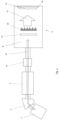
- the device shown for implanting particles into a substrate comprises a particle source 2, a particle accelerator 4, and a terminal station 6 with an irradiation chamber 8.
- a high vacuum is typically present in the irradiation chamber 8.
- a substrate 12 to be doped is held in the irradiation chamber 8 in a substrate holder 30.
- the material of the substrate 12 is preferably silicon carbide (SiC).
- SiC silicon carbide
- other semiconductor materials such as silicon, gallium arsenide, cadmium telluride, zinc selenide, gallium nitride, etc. are also possible.
- Non-semiconducting materials such as quartz glass, lithium niobate, potassium titanyl phosphate, or even plastics such as PMMA are also conceivable as the material of the substrate 12.
- the substrate 12 is preferably formed as a wafer.
- ions preferably with a positive charge, are generated.
- the desired ion type is selected by the analyzing magnet 3.
- the positively charged ions are then accelerated by the particle accelerator 4, forming the accelerated ion beam 10.
- the ions of the ion beam 10 are preferably made of aluminum, nitrogen, hydrogen, helium, boron, phosphorus, carbon, arsenic, or vanadium.
- the particle accelerator 4 is preferably a high-frequency linear accelerator in which the ions are accelerated using high-frequency fields.
- the particle accelerator 4 can also be configured as a cyclotron or an electrostatic accelerator, such as a tandem accelerator, tandemtron accelerator, or single-ended electrostatic accelerator.
- electrostatic tandemtron design negative ions are first generated in the particle source 2, accelerated, recharged at a high-voltage terminal, and then accelerated again, analogously to the case described above.
- the particle accelerator 4 is designed as a simple high-frequency linear accelerator or as a cyclotron, which can only accelerate the ion beam 10 to a fixed energy per nucleon. Due to its design, the control unit of the high-frequency linear accelerator or cyclotron cannot change the energy per nucleon, but serves only to control the energy required for the operation of the system. necessary parameters. It is also conceivable that, due to the design, fewer than ten, preferably a maximum of five, adjustable energies of the ion beam 10 are possible. This significantly reduces the control effort in the particle accelerator 4 compared to a free variation of the energy of the ion beam 10 supplied by the particle accelerator.
- the high-frequency linear accelerator or cyclotron preferably delivers a pulsed ion beam 10 of positively charged ions with an energy of 0.3 to 3.0 MeV/nucleon, preferably 0.5 to 3.0 MeV/nucleon, more preferably 1.0 to 2.0 MeV/nucleon, and particularly preferably 1.3 to 1.7 MeV per nucleon.
- the ion beam 10 thus generated can be described by a duty cycle of the ion current within a time window.
- the duty cycle (on:off) of the ion beam 10 can be between 1:20 and 1:5, preferably between 1:12 and 1:8.
- a duty cycle of 1:10 is explained. Since only 10% of the time window is available for effective irradiation, a current of 100 ⁇ A must be maintained within the pulse for such a pulsed ion beam if an average ion current of 10 ⁇ A is to be achieved.
- the frequency of the pulses of the ion beam 10 is between 1 Hz and 2 kHz, preferably between 3 Hz and 500 Hz, and particularly preferably between 7 Hz and 200 Hz.
- the ion beam 10 can also be continuous at the same energy.
- the high-energy ion beam 10 is typically shaped in an ion optics 14 before entering the end station 6 and then guided into the irradiation chamber 8. There, the energy of the ion beam 10 is spread by an energy filter 20 and impinges on the substrate 12 to be irradiated.
- the substrate holder 30 does not have to be stationary, but can optionally be provided with a device for displacing the substrate 12 in xy (in the plane perpendicular to the plane of the page).
- a wafer wheel, on which the substrates 12 to be implanted are fixed and which rotates during implantation, can also be considered as the substrate holder 30.
- 30 in the beam direction (z-direction) may be possible.
- the substrate holder 30 can optionally be equipped with a heating or cooling system.
- the basic principle of the energy filter 20 is Fig. 2
- the monoenergetic ion beam 10 is modified in its energy as it passes through the energy filter 20, which is designed as a microstructured membrane, depending on the entry point.
- the resulting energy distribution of the ions of the ion beam 10 leads to a modification of the depth profile of the implanted substance in the matrix of the substrate 12.
- E1 denotes the energy of a first ion
- E2 denotes the energy of a second ion
- c denotes the doping concentration
- d denotes the depth in the substrate 12.
- the usual Gaussian distribution is designated by reference symbol A, which is created without the use of an energy filter 20.
- a rectangular distribution which can be achieved using an energy filter 20, is sketched as an example with reference symbol B.
- the layouts or three-dimensional structures of energy filters 20 shown show the basic possibilities of generating a plurality of dopant depth profiles or defect depth profiles using energy filters 20.
- c again denotes the doping concentration
- d again denotes the depth in the substrate 12.
- the filter structure profiles can, in principle, be combined with one another to obtain new filter structure profiles and thus new dopant depth profiles or defect depth profiles.
- Such energy filters 20 are generally made of silicon. They have a thickness of between 3 ⁇ m and 200 ⁇ m, preferably between 5 ⁇ m and 50 ⁇ m, and particularly preferably between 7 ⁇ m and 20 ⁇ m. They can be held in a filter frame (not shown). The filter frame can be exchangeably mounted in a filter holder 16 (see Fig. 4 ) must be included.
- At least one passive deceleration element 22 is arranged in the beam path of the ion beam 10.
- the deceleration element 22 is arranged between the particle accelerator 4 and the substrate holder 30 and spaced from the energy filter 20.
- the passive deceleration element 22 comprises a planar membrane made of one of the following materials: silicon, tungsten, carbon, titanium. Criteria for material selection include the manufacturability of thin membranes, the braking capacity of the material, the heat capacity or heat radiation capacity of the material and the potential risk of contamination of the substrate 12.
- the thickness of the planar membrane is between 0.5 ⁇ m and 100 ⁇ m, preferably between 2 ⁇ m and 30 ⁇ m, and more preferably between 4 ⁇ m and 15 ⁇ m.
- Each braking element 22 may be held in a frame (not shown).
- the frame may be replaceably mounted in the holder 18 (see Fig. 4 ) must be included.
- Fig. 1 exactly one passive braking element 22 is shown, which is arranged between the particle accelerator 4 and the energy filter 20 and preferably within the irradiation chamber 8.
- Fig. 4 shows a section of an alternative embodiment of the device from Fig. 1 . Identical elements are provided with the same reference numerals. Unless otherwise stated, the above-mentioned Fig. 1 statements made, as well as to components not shown.
- the ion beam 10 is preferably expanded in a beam expansion device 24 before impinging on the deceleration element 22 or on the energy filter 20.
- a plurality of passive deceleration elements 22 are provided. As shown, deceleration elements 22 can be arranged in front of or behind the energy filter 20 in the beam direction and are usually held by a holder 18.
- Each of the braking elements 22 is arranged at a distance from the next braking element 22 or from the energy filter 20.
- the distance between two consecutive braking elements 22 or between a braking element 22 and the energy filter 20 is typically between 0.5 cm and 50 cm, preferably between 0.7 cm and 10 cm, and more preferably between 1 cm and 2 cm.
- each passive deceleration element 22 can be mounted so as to be displaceable perpendicular to the beam direction.
- the mounts 18 are not shown for the sake of simplicity.
- the number of deceleration elements 22 through which the ion beam 10 passes after the particle accelerator 4 can now be varied, for example.
- a variation in the energy of the ion beam 10 impinging on the substrate 12 can be achieved by a suitable selection of properties, such as material and/or thickness, of the deceleration element 22 or the deceleration elements 22.
- all of the above-mentioned parameters must be adjusted so that the deceleration capacity of all deceleration elements 22 and the energy filter 20 in the beam path is selected such that the energy of the ion beam 10 is reduced to the desired energy for the respective application (depth of the dopant profile or defect profile in the substrate 12).
- the selection and design of the deceleration elements 22, together with the energy filter 20, thus significantly determines the primary energy of the ion beam 10 for the respective application, based on the fixed energy per nucleon supplied by the accelerator.
- a passive braking unit 28 which is preferably designed as a planar membrane layer, to the energy filter 20.
- the braking unit 28 is also preferably made of silicon. This avoids stress effects that can arise from the different thermal expansion behavior of different materials.
- embodiments of the energy filter 20 and the braking unit 28 are also conceivable that provide different materials for the energy filter 20 and the braking unit 28. In such cases, the energy filter 20 and the braking unit 28 cannot be constructed monolithically; instead, a mechanically strong, highly thermally conductive connection must exist between the energy filter 20 and the braking unit 28.
- Fig. 5 corresponds in many aspects to the embodiment of Fig. 4 .
- a device has been added which enables a rotational movement of one or more braking elements 22 and/or one or more energy filters 20.
- At least one braking element 22 and/or at least one energy filter 20 is attached to a shaft 34, which in turn is rotatably mounted and driven by a rotating mechanism 32.
- the respective braking element 22 and/or the respective energy filter 20 can be moved into or out of the beam path.
- a servomotor is particularly suitable as the drive component of the rotating mechanism 34.
- a braking element 22 is provided in multiple, preferably identical, versions, and these braking elements 22 are alternately rotated into the path of the ion beam 10.
- several, preferably identical, energy filters 20 can also be provided, which are alternately brought into the path of the ion beam 10.
- the holders 16, 18 of energy filters 20 and braking elements 22 can also be formed integrally with one another.
- the movement of the energy filters 20 and/or the passive deceleration elements 22 is advantageously tuned to the periodic temporal structure of the ion beam 10. This ensures that the ion pulse always hits active areas of the energy filter 20 or the deceleration elements 22, and prevents the ion pulse from always hitting the same point on an energy filter 20 or a deceleration element 22.
- the tuning can be achieved by a rotational movement per pulse or per multiple pulses, for example, in a range per 10-20 pulses.
- the timing of pulsed ion beam 10 and rotating energy filters 20 and/or deceleration elements 22 should result in energy filters 20 and/or deceleration elements 22 being irradiated evenly on average, the energy input being distributed as evenly as possible, and dead times caused by inadvertently irradiated auxiliary or holding structures of the energy filters 20 or the deceleration elements 22 being avoided.
- a rotational movement is necessary at very high ion currents and very large differences between the accelerator-side and substrate-side energies of the ion beam 10. In these cases, a deceleration element 22 and/or an energy filter 20 would heat up considerably. It is therefore necessary to increase the effective area impinged by the accelerator-side ion beam 10 or to reduce the impinging current density.
- Dissipated power energy converted into heat in the element
- radiated power minus transmitted power residual power after passing through the element
- the alternating use of identical braking elements 22 or the alternating use of identical energy filters 20 is useful for dissipated powers above 3 W/cm 2 , preferably already above 2 W/cm 2 .
- One aspect of the device according to the invention is the use of structured energy filters 20 together with non-structured deceleration elements 20 for energy modification.
- This can be used to drastically simplify particle accelerators 4, since they can be constructed in such a way that, for example, only a fixed energy needs to be delivered per nucleon.
- the application-specific target energy of the ion beam 10 is then adjusted by targeted energy subtraction from the energy of the primary beam.
- deceleration elements 22 can vary in each of the embodiments described above, as can their spatial arrangement and properties such as material and thickness. At least one deceleration element 22 must be present, which can be arranged in front of and/or behind the energy filter 20 in the beam direction. Certain individual deceleration elements 22 from the embodiments described above can also be used separately or in any combination with other deceleration elements 22 from other embodiments.
- the individual braking elements 22 may differ in their properties or they may be identical.
- the braking elements 22 and/or the energy filter 20 can also be displaceable in the beam direction, either individually relative to one another or together as a whole.
- the braking elements 22 and energy filters 20 can also be arranged in a separate vacuum chamber that can be closed by valves and is arranged within the irradiation chamber 8 or directly adjacent to it.
Landscapes
- Chemical & Material Sciences (AREA)
- Analytical Chemistry (AREA)
- Particle Accelerators (AREA)
- Physical Vapour Deposition (AREA)
- Physical Or Chemical Processes And Apparatus (AREA)
Claims (13)
- Dispositif d'implantation de particules dans un substrat (12), comportantune source de particules (2) et un accélérateur de particules (4) pour générer un faisceau d'ions (10) d'ions chargés positivement ;un support de substrat (30) ;un filtre d'énergie (20), qui est disposé entre l'accélérateur de particules (4) et le support de substrat (30), dans lequel le filtre d'énergie (20) est une membrane microstructurée avec un profil structurel prédéfini pour ajuster un profil de profondeur de dopant et/ou un profil de profondeur de défaut dans le substrat (12) provoqué par l'implantation ; etau moins un élément de décélération passif (22) pour le faisceau d'ions (10), qui est disposé entre l'accélérateur de particules (4) et le support de substrat (30) et espacé du filtre d'énergie (20), dans lequel le au moins un élément de décélération passif (22) est disposé entre l'accélérateur de particules (4) et le filtre d'énergie (20) et/ou est disposé derrière le filtre d'énergie (20) dans la direction du faisceau,caractérisé en ce que le au moins un élément de décélération passif (22) est positionné de manière pivotante ou déplaçable, afin de produire une variation de l'énergie du faisceau d'ions frappant le substrat (12) même avec une énergie fixe du faisceau d'ions (10) fourni par l'accélérateur de particules (4).
- Dispositif selon la revendication 1, caractérisé en ce que le au moins un élément de décélération passif (22) comporte une membrane plane.
- Dispositif selon la revendication 2, caractérisé en ce que l'épaisseur de la membrane plane est comprise entre 0,5 µm et 100 µm, de préférence entre 2 µm et 30 µm, plus préférentiellement entre 4 µm et 15 µm.
- Dispositif selon la revendication 2 ou 3, caractérisé en ce que le matériau de la membrane plane est choisi parmi un des matériaux suivants : silicium, tungstène, carbone, titane.
- Dispositif selon une des revendications précédentes, caractérisé en ce que l'accélérateur de particules (4) est un accélérateur linéaire à haute fréquence ou un cyclotron.
- Dispositif selon la revendication 5, caractérisé en ce que l'accélérateur de particules (4) génère un faisceau d'ions (10) pulsé ou continu d'une énergie de 0,3 à 3,0 MeV/nucléon, de préférence de 0,5 à 3,0 MeV/nucléon, plus préférentiellement de 1,0 à 2,0 MeV/nucléon, plus préférentiellement de 1,3 à 1,7 MeV/nucléon.
- Dispositif selon la revendication 5 ou 6, caractérisé en ce que l'accélérateur de particules (4), de par sa conception, ne fournit qu'une énergie fixe par nucléon pour chaque type d'ion ou que l'accélérateur de particules (4) de par sa conception ne peut délivrer que des ions dans la gamme d'énergie de 1 à 50 Mev, de sorte que, de par sa conception, moins de dix énergies ajustables du faisceau d'ions (10) sont possibles.
- Dispositif selon une des revendications précédentes, caractérisé en ce que les supports (16, 18) du filtre d'énergie (20) et du au moins un élément de décélération (22) sont formés en un seul tenant l'un avec l'autre.
- Dispositif selon une des revendications précédentes, caractérisé en ce que le au moins un élément de décélération (22) et le filtre d'énergie (20) sont disposés dans une chambre à vide séparée, qui peut être fermée par des vannes et qui est disposée à l'intérieur de la chambre d'irradiation (8) ou directement juxtaposée à la chambre d'irradiation (8).
- Procédé d'implantation de particules dans un substrat (12) utilisant le dispositif selon une quelconque des revendications 1 à 9, comprenant les étapes suivantes :- la génération d'un faisceau d'ions (10) d'ions chargés positivement au moyen d'une source de particules (2) et d'un accélérateur de particules (4) ; et- l'irradiation du substrat (12) maintenu par le support de substrat (30) avec le faisceau d'ions (10) en interposant le au moins un élément de décélération passif (22) et le filtre d'énergie (20).
- Procédé selon la revendication 10, caractérisé en ce qu'une variation de l'énergie du faisceau d'ions (10) frappant le substrat (12) est déterminée en utilisant une sélection appropriée du nombre et des propriétés, telles que le matériau et/ou l'épaisseur de l'élément de décélération (22) ou des éléments de décélération (22), à travers lesquels le faisceau d'ions (10) passe après l'accélérateur de particules (4).
- Procédé selon la revendication 10 ou 11, caractérisé en ce qu'un élément de décélération (22) est présent en plusieurs exemplaires et ces éléments de décélération (22) sont amenés alternativement, de préférence tournés, sur le trajet du faisceau d'ions (10).
- Procédé selon la revendication 12, caractérisé en ce que plusieurs filtres d'énergie (20) sont présents, qui sont amenés alternativement sur le trajet du faisceau d'ions (10), dans lequel les filtres d'énergie (20) et les éléments de décélération (22) sont entraînés par le même mécanisme de rotation (32).
Priority Applications (1)
| Application Number | Priority Date | Filing Date | Title |
|---|---|---|---|
| EP25161322.0A EP4539092A3 (fr) | 2019-05-15 | 2020-05-14 | Dispositif et procédé d'implantation de particules dans un substrat |
Applications Claiming Priority (2)
| Application Number | Priority Date | Filing Date | Title |
|---|---|---|---|
| DE102019112773.4A DE102019112773B4 (de) | 2019-05-15 | 2019-05-15 | Vorrichtung und Verfahren zur Implantation von Teilchen in ein Substrat |
| PCT/EP2020/063555 WO2020229638A2 (fr) | 2019-05-15 | 2020-05-14 | Dispositif et procédé d'implantation de particules dans un substrat |
Related Child Applications (2)
| Application Number | Title | Priority Date | Filing Date |
|---|---|---|---|
| EP25161322.0A Division EP4539092A3 (fr) | 2019-05-15 | 2020-05-14 | Dispositif et procédé d'implantation de particules dans un substrat |
| EP25161322.0A Division-Into EP4539092A3 (fr) | 2019-05-15 | 2020-05-14 | Dispositif et procédé d'implantation de particules dans un substrat |
Publications (3)
| Publication Number | Publication Date |
|---|---|
| EP3970180A2 EP3970180A2 (fr) | 2022-03-23 |
| EP3970180B1 true EP3970180B1 (fr) | 2025-05-07 |
| EP3970180C0 EP3970180C0 (fr) | 2025-05-07 |
Family
ID=70857143
Family Applications (2)
| Application Number | Title | Priority Date | Filing Date |
|---|---|---|---|
| EP20728419.1A Active EP3970180B1 (fr) | 2019-05-15 | 2020-05-14 | Dispositif et procédé d'implantation de particules dans un substrat |
| EP25161322.0A Pending EP4539092A3 (fr) | 2019-05-15 | 2020-05-14 | Dispositif et procédé d'implantation de particules dans un substrat |
Family Applications After (1)
| Application Number | Title | Priority Date | Filing Date |
|---|---|---|---|
| EP25161322.0A Pending EP4539092A3 (fr) | 2019-05-15 | 2020-05-14 | Dispositif et procédé d'implantation de particules dans un substrat |
Country Status (6)
| Country | Link |
|---|---|
| US (1) | US12125670B2 (fr) |
| EP (2) | EP3970180B1 (fr) |
| JP (2) | JP7210071B2 (fr) |
| CN (1) | CN113811975B (fr) |
| DE (1) | DE102019112773B4 (fr) |
| WO (1) | WO2020229638A2 (fr) |
Families Citing this family (2)
| Publication number | Priority date | Publication date | Assignee | Title |
|---|---|---|---|---|
| EP4238121A1 (fr) * | 2020-12-17 | 2023-09-06 | MI2-Factory GmbH | Ensemble filtre d'énergie pour système d'implantation ionique comportant au moins un élément d'accouplement |
| US11569063B2 (en) | 2021-04-02 | 2023-01-31 | Applied Materials, Inc. | Apparatus, system and method for energy spread ion beam |
Family Cites Families (16)
| Publication number | Priority date | Publication date | Assignee | Title |
|---|---|---|---|---|
| US4278475A (en) * | 1979-01-04 | 1981-07-14 | Westinghouse Electric Corp. | Forming of contoured irradiated regions in materials such as semiconductor bodies by nuclear radiation |
| JP2526941B2 (ja) * | 1987-11-24 | 1996-08-21 | 日新電機株式会社 | イオン注入装置 |
| JP2007523440A (ja) | 2004-02-18 | 2007-08-16 | 学校法人早稲田大学 | イオン注入方法及び装置 |
| US7435977B2 (en) * | 2005-12-12 | 2008-10-14 | Axcelis Technologies, Inc. | Ion beam angle measurement systems and methods for ion implantation systems |
| DE102005061663B4 (de) | 2005-12-22 | 2008-07-17 | RUHR-UNIVERSITäT BOCHUM | Ionenimplantationsvorrichtung |
| US20080128641A1 (en) * | 2006-11-08 | 2008-06-05 | Silicon Genesis Corporation | Apparatus and method for introducing particles using a radio frequency quadrupole linear accelerator for semiconductor materials |
| CN101536616A (zh) * | 2006-11-08 | 2009-09-16 | 硅源公司 | 采用射频四极线性加速器引入用于半导体材料的粒子的设备和方法 |
| DE102010019871B4 (de) | 2010-05-07 | 2018-07-12 | A. Kayser Automotive Systems Gmbh | Filtrationsvorrichtung |
| DE102011075350A1 (de) | 2011-05-05 | 2012-11-08 | Fachhochschule Jena | Energiefilteranordnung für Ionenimplantationsanlagen |
| JP6057534B2 (ja) * | 2012-04-18 | 2017-01-11 | 住重試験検査株式会社 | 半導体装置の製造方法 |
| DE102015202121B4 (de) | 2015-02-06 | 2017-09-14 | Infineon Technologies Ag | SiC-basierte Supersperrschicht-Halbleitervorrichtungen und Verfahren zur Herstellung dieser |
| DE102016106119B4 (de) | 2016-04-04 | 2019-03-07 | mi2-factory GmbH | Energiefilterelement für Ionenimplantationsanlagen für den Einsatz in der Produktion von Wafern |
| DE102016110429A1 (de) * | 2016-06-06 | 2017-12-07 | Infineon Technologies Ag | Energiefilter zum Verarbeiten einer Leistungshalbleitervorrichtung |
| DE102016122791B3 (de) | 2016-11-25 | 2018-05-30 | mi2-factory GmbH | Ionenimplantationsanlage, Filterkammer und Implantationsverfahren unter Einsatz eines Energiefilterelements |
| JP6785188B2 (ja) * | 2017-05-31 | 2020-11-18 | 住友重機械イオンテクノロジー株式会社 | イオン注入装置およびイオン注入方法 |
| JP6925729B2 (ja) * | 2017-08-22 | 2021-08-25 | 住重アテックス株式会社 | 半導体装置の製造方法 |
-
2019
- 2019-05-15 DE DE102019112773.4A patent/DE102019112773B4/de active Active
-
2020
- 2020-05-14 EP EP20728419.1A patent/EP3970180B1/fr active Active
- 2020-05-14 EP EP25161322.0A patent/EP4539092A3/fr active Pending
- 2020-05-14 JP JP2021563676A patent/JP7210071B2/ja active Active
- 2020-05-14 US US17/610,811 patent/US12125670B2/en active Active
- 2020-05-14 CN CN202080034328.9A patent/CN113811975B/zh active Active
- 2020-05-14 WO PCT/EP2020/063555 patent/WO2020229638A2/fr not_active Ceased
-
2022
- 2022-12-07 JP JP2022195434A patent/JP7450975B2/ja active Active
Also Published As
| Publication number | Publication date |
|---|---|
| JP2022532999A (ja) | 2022-07-21 |
| EP4539092A3 (fr) | 2025-07-23 |
| EP3970180A2 (fr) | 2022-03-23 |
| EP3970180C0 (fr) | 2025-05-07 |
| US20220199362A1 (en) | 2022-06-23 |
| DE102019112773B4 (de) | 2023-11-30 |
| JP7210071B2 (ja) | 2023-01-23 |
| WO2020229638A2 (fr) | 2020-11-19 |
| CN113811975B (zh) | 2025-05-16 |
| US12125670B2 (en) | 2024-10-22 |
| WO2020229638A3 (fr) | 2021-01-07 |
| CN113811975A (zh) | 2021-12-17 |
| JP2023029981A (ja) | 2023-03-07 |
| JP7450975B2 (ja) | 2024-03-18 |
| DE102019112773A1 (de) | 2020-11-19 |
| EP4539092A2 (fr) | 2025-04-16 |
Similar Documents
| Publication | Publication Date | Title |
|---|---|---|
| DE2120401C2 (de) | Verfahren und Vorrichtung zur Trennung von zwei Isotopen eines Stoffes | |
| EP3079803B1 (fr) | Dispositif d'application d'électrons accélérés à un produit en vrac | |
| AT393334B (de) | Anordnung zur stabilisierung einer bestrahlten maske | |
| DE102013111650B3 (de) | Vorrichtung zum Erzeugen beschleunigter Elektronen | |
| DE112011100403B4 (de) | Ultraschnelle Elektronenbeugungsvorrichtung und Verfahren zur ultraschnellen Elektronenbeugung | |
| EP3590125B1 (fr) | Dispositif pour produire des électrons accélérés | |
| EP3836188B1 (fr) | Procédé et dispositif d'implantation ionique dans des plaquettes semi-conductrices | |
| DE2335821A1 (de) | Teilchenbeschleuniger | |
| DE1489135B2 (de) | Verfahren zum Ändern der Dotierung von mindestens einem Teil eines einkristallinen Halbleiterkörpers | |
| EP4539092A2 (fr) | Dispositif et procédé d'implantation de particules dans un substrat | |
| EP1872372B1 (fr) | Cylindre creux soumis a l'action d'un rayonnement laser, utilise en tant que lentille pour faisceaux d'ions | |
| DE102010048276A1 (de) | Ionentransporter, Ionentransportverfahren, Ionenstrahlstrahler und medizinischer Teilchenstrahlstrahler | |
| EP3642861B1 (fr) | Dispositif de génération d'électrons accélérés | |
| DE3114644A1 (de) | Verfahren und vorrichtung zur erzeugung von elektronenimpulsen hoher dichte | |
| EP3570310B1 (fr) | Dispositif de production d'électrons accélérés | |
| DE19518717C2 (de) | Vorrichtung zum Bestrahlen von Oberflächen mit Elektronen | |
| DE102016109171B4 (de) | Vorrichtung zur Verstärkung von Mikro-Elektronenpaket-Instabilitäten | |
| EP3043370A1 (fr) | Dispositif d'extraction des particules chargées d'un espace de production et procédé d'utilisation d'un tel dispositif | |
| EP2586052B1 (fr) | Dispositif permettant de structurer des surfaces de corps solides au moyen de faisceaux ioniques provenant d'un spectre de faisceaux ioniques | |
| DE102019118657B4 (de) | Vorrichtung zur Erzeugung einer Elektronenstrahlung sowie 3D-Druck-Vorrichtung | |
| DE102019203493A1 (de) | Verfahren zur ultrahochaufgelösten Modifikation, insbesondere zur physischen Materialabtragung oder internen Materialänderung, eines Werkstücks | |
| DE102009005620B4 (de) | Verfahren und Anordnung zur Erzeugung eines Elektronenstrahls | |
| DE102010023632B4 (de) | Vorrichtung und Verfahren zur Erzeugung elektromagnetischer Strahlung | |
| WO2011070156A2 (fr) | Dispositif et procédé de modification d'un substrat semiconducteur par un faisceau d'ions | |
| DE102018106412A1 (de) | Teilchenspektrometer und Teilchenspektrometrieverfahren |
Legal Events
| Date | Code | Title | Description |
|---|---|---|---|
| STAA | Information on the status of an ep patent application or granted ep patent |
Free format text: STATUS: UNKNOWN |
|
| STAA | Information on the status of an ep patent application or granted ep patent |
Free format text: STATUS: THE INTERNATIONAL PUBLICATION HAS BEEN MADE |
|
| PUAI | Public reference made under article 153(3) epc to a published international application that has entered the european phase |
Free format text: ORIGINAL CODE: 0009012 |
|
| STAA | Information on the status of an ep patent application or granted ep patent |
Free format text: STATUS: REQUEST FOR EXAMINATION WAS MADE |
|
| 17P | Request for examination filed |
Effective date: 20211029 |
|
| AK | Designated contracting states |
Kind code of ref document: A2 Designated state(s): AL AT BE BG CH CY CZ DE DK EE ES FI FR GB GR HR HU IE IS IT LI LT LU LV MC MK MT NL NO PL PT RO RS SE SI SK SM TR |
|
| DAV | Request for validation of the european patent (deleted) | ||
| DAX | Request for extension of the european patent (deleted) | ||
| GRAP | Despatch of communication of intention to grant a patent |
Free format text: ORIGINAL CODE: EPIDOSNIGR1 |
|
| STAA | Information on the status of an ep patent application or granted ep patent |
Free format text: STATUS: GRANT OF PATENT IS INTENDED |
|
| INTG | Intention to grant announced |
Effective date: 20241205 |
|
| GRAS | Grant fee paid |
Free format text: ORIGINAL CODE: EPIDOSNIGR3 |
|
| GRAA | (expected) grant |
Free format text: ORIGINAL CODE: 0009210 |
|
| STAA | Information on the status of an ep patent application or granted ep patent |
Free format text: STATUS: THE PATENT HAS BEEN GRANTED |
|
| RAP3 | Party data changed (applicant data changed or rights of an application transferred) |
Owner name: MI2-FACTORY GMBH |
|
| AK | Designated contracting states |
Kind code of ref document: B1 Designated state(s): AL AT BE BG CH CY CZ DE DK EE ES FI FR GB GR HR HU IE IS IT LI LT LU LV MC MK MT NL NO PL PT RO RS SE SI SK SM TR |
|
| REG | Reference to a national code |
Ref country code: GB Ref legal event code: FG4D Free format text: NOT ENGLISH |
|
| REG | Reference to a national code |
Ref country code: CH Ref legal event code: EP |
|
| REG | Reference to a national code |
Ref country code: IE Ref legal event code: FG4D Free format text: LANGUAGE OF EP DOCUMENT: GERMAN |
|
| U01 | Request for unitary effect filed |
Effective date: 20250507 |
|
| U07 | Unitary effect registered |
Designated state(s): AT BE BG DE DK EE FI FR IT LT LU LV MT NL PT RO SE SI Effective date: 20250513 |
|
| U20 | Renewal fee for the european patent with unitary effect paid |
Year of fee payment: 6 Effective date: 20250528 |
|
| PG25 | Lapsed in a contracting state [announced via postgrant information from national office to epo] |
Ref country code: ES Free format text: LAPSE BECAUSE OF FAILURE TO SUBMIT A TRANSLATION OF THE DESCRIPTION OR TO PAY THE FEE WITHIN THE PRESCRIBED TIME-LIMIT Effective date: 20250507 |
|
| PG25 | Lapsed in a contracting state [announced via postgrant information from national office to epo] |
Ref country code: NO Free format text: LAPSE BECAUSE OF FAILURE TO SUBMIT A TRANSLATION OF THE DESCRIPTION OR TO PAY THE FEE WITHIN THE PRESCRIBED TIME-LIMIT Effective date: 20250807 Ref country code: GR Free format text: LAPSE BECAUSE OF FAILURE TO SUBMIT A TRANSLATION OF THE DESCRIPTION OR TO PAY THE FEE WITHIN THE PRESCRIBED TIME-LIMIT Effective date: 20250808 |
|
| PG25 | Lapsed in a contracting state [announced via postgrant information from national office to epo] |
Ref country code: PL Free format text: LAPSE BECAUSE OF FAILURE TO SUBMIT A TRANSLATION OF THE DESCRIPTION OR TO PAY THE FEE WITHIN THE PRESCRIBED TIME-LIMIT Effective date: 20250507 |
|
| PG25 | Lapsed in a contracting state [announced via postgrant information from national office to epo] |
Ref country code: HR Free format text: LAPSE BECAUSE OF FAILURE TO SUBMIT A TRANSLATION OF THE DESCRIPTION OR TO PAY THE FEE WITHIN THE PRESCRIBED TIME-LIMIT Effective date: 20250507 |
|
| PG25 | Lapsed in a contracting state [announced via postgrant information from national office to epo] |
Ref country code: RS Free format text: LAPSE BECAUSE OF FAILURE TO SUBMIT A TRANSLATION OF THE DESCRIPTION OR TO PAY THE FEE WITHIN THE PRESCRIBED TIME-LIMIT Effective date: 20250807 |
|
| PG25 | Lapsed in a contracting state [announced via postgrant information from national office to epo] |
Ref country code: IS Free format text: LAPSE BECAUSE OF FAILURE TO SUBMIT A TRANSLATION OF THE DESCRIPTION OR TO PAY THE FEE WITHIN THE PRESCRIBED TIME-LIMIT Effective date: 20250907 |
|
| REG | Reference to a national code |
Ref country code: CH Ref legal event code: H13 Free format text: ST27 STATUS EVENT CODE: U-0-0-H10-H13 (AS PROVIDED BY THE NATIONAL OFFICE) Effective date: 20251223 |
|
| PG25 | Lapsed in a contracting state [announced via postgrant information from national office to epo] |
Ref country code: SM Free format text: LAPSE BECAUSE OF FAILURE TO SUBMIT A TRANSLATION OF THE DESCRIPTION OR TO PAY THE FEE WITHIN THE PRESCRIBED TIME-LIMIT Effective date: 20250507 |
|
| PG25 | Lapsed in a contracting state [announced via postgrant information from national office to epo] |
Ref country code: CH Free format text: LAPSE BECAUSE OF NON-PAYMENT OF DUE FEES Effective date: 20250531 |
|
| PG25 | Lapsed in a contracting state [announced via postgrant information from national office to epo] |
Ref country code: CZ Free format text: LAPSE BECAUSE OF FAILURE TO SUBMIT A TRANSLATION OF THE DESCRIPTION OR TO PAY THE FEE WITHIN THE PRESCRIBED TIME-LIMIT Effective date: 20250507 |
|
| PG25 | Lapsed in a contracting state [announced via postgrant information from national office to epo] |
Ref country code: SK Free format text: LAPSE BECAUSE OF FAILURE TO SUBMIT A TRANSLATION OF THE DESCRIPTION OR TO PAY THE FEE WITHIN THE PRESCRIBED TIME-LIMIT Effective date: 20250507 |
|
| PG25 | Lapsed in a contracting state [announced via postgrant information from national office to epo] |
Ref country code: MC Free format text: LAPSE BECAUSE OF FAILURE TO SUBMIT A TRANSLATION OF THE DESCRIPTION OR TO PAY THE FEE WITHIN THE PRESCRIBED TIME-LIMIT Effective date: 20250507 |
|
| PLBE | No opposition filed within time limit |
Free format text: ORIGINAL CODE: 0009261 |
|
| STAA | Information on the status of an ep patent application or granted ep patent |
Free format text: STATUS: NO OPPOSITION FILED WITHIN TIME LIMIT |
|
| REG | Reference to a national code |
Ref country code: CH Ref legal event code: L10 Free format text: ST27 STATUS EVENT CODE: U-0-0-L10-L00 (AS PROVIDED BY THE NATIONAL OFFICE) Effective date: 20260318 |
|
| PG25 | Lapsed in a contracting state [announced via postgrant information from national office to epo] |
Ref country code: IE Free format text: LAPSE BECAUSE OF NON-PAYMENT OF DUE FEES Effective date: 20250514 |
|
| 26N | No opposition filed |
Effective date: 20260210 |
|
| GBPC | Gb: european patent ceased through non-payment of renewal fee |
Effective date: 20250807 |
|
| U20 | Renewal fee for the european patent with unitary effect paid |
Year of fee payment: 7 Effective date: 20260327 |