EP3962045A1 - Fotografieranordnung unter einem bildschirm sowie entsprechender organischer leuchtdiodenanzeigeschirm und endgerät - Google Patents
Fotografieranordnung unter einem bildschirm sowie entsprechender organischer leuchtdiodenanzeigeschirm und endgerät Download PDFInfo
- Publication number
- EP3962045A1 EP3962045A1 EP20794749.0A EP20794749A EP3962045A1 EP 3962045 A1 EP3962045 A1 EP 3962045A1 EP 20794749 A EP20794749 A EP 20794749A EP 3962045 A1 EP3962045 A1 EP 3962045A1
- Authority
- EP
- European Patent Office
- Prior art keywords
- layer
- light
- screen
- area
- hole
- Prior art date
- Legal status (The legal status is an assumption and is not a legal conclusion. Google has not performed a legal analysis and makes no representation as to the accuracy of the status listed.)
- Pending
Links
Images


Classifications
-
- H—ELECTRICITY
- H04—ELECTRIC COMMUNICATION TECHNIQUE
- H04M—TELEPHONIC COMMUNICATION
- H04M1/00—Substation equipment, e.g. for use by subscribers
- H04M1/02—Constructional features of telephone sets
- H04M1/0202—Portable telephone sets, e.g. cordless phones, mobile phones or bar type handsets
- H04M1/026—Details of the structure or mounting of specific components
- H04M1/0264—Details of the structure or mounting of specific components for a camera module assembly
-
- H—ELECTRICITY
- H04—ELECTRIC COMMUNICATION TECHNIQUE
- H04N—PICTORIAL COMMUNICATION, e.g. TELEVISION
- H04N23/00—Cameras or camera modules comprising electronic image sensors; Control thereof
- H04N23/50—Constructional details
- H04N23/55—Optical parts specially adapted for electronic image sensors; Mounting thereof
-
- H—ELECTRICITY
- H04—ELECTRIC COMMUNICATION TECHNIQUE
- H04N—PICTORIAL COMMUNICATION, e.g. TELEVISION
- H04N23/00—Cameras or camera modules comprising electronic image sensors; Control thereof
- H04N23/57—Mechanical or electrical details of cameras or camera modules specially adapted for being embedded in other devices
-
- H—ELECTRICITY
- H10—SEMICONDUCTOR DEVICES; ELECTRIC SOLID-STATE DEVICES NOT OTHERWISE PROVIDED FOR
- H10K—ORGANIC ELECTRIC SOLID-STATE DEVICES
- H10K50/00—Organic light-emitting devices
- H10K50/10—OLEDs or polymer light-emitting diodes [PLED]
- H10K50/14—Carrier transporting layers
- H10K50/15—Hole transporting layers
-
- H—ELECTRICITY
- H10—SEMICONDUCTOR DEVICES; ELECTRIC SOLID-STATE DEVICES NOT OTHERWISE PROVIDED FOR
- H10K—ORGANIC ELECTRIC SOLID-STATE DEVICES
- H10K50/00—Organic light-emitting devices
- H10K50/10—OLEDs or polymer light-emitting diodes [PLED]
- H10K50/14—Carrier transporting layers
- H10K50/16—Electron transporting layers
-
- H—ELECTRICITY
- H10—SEMICONDUCTOR DEVICES; ELECTRIC SOLID-STATE DEVICES NOT OTHERWISE PROVIDED FOR
- H10K—ORGANIC ELECTRIC SOLID-STATE DEVICES
- H10K50/00—Organic light-emitting devices
- H10K50/10—OLEDs or polymer light-emitting diodes [PLED]
- H10K50/17—Carrier injection layers
- H10K50/171—Electron injection layers
-
- H—ELECTRICITY
- H10—SEMICONDUCTOR DEVICES; ELECTRIC SOLID-STATE DEVICES NOT OTHERWISE PROVIDED FOR
- H10K—ORGANIC ELECTRIC SOLID-STATE DEVICES
- H10K50/00—Organic light-emitting devices
- H10K50/80—Constructional details
- H10K50/868—Arrangements for polarized light emission
-
- H—ELECTRICITY
- H10—SEMICONDUCTOR DEVICES; ELECTRIC SOLID-STATE DEVICES NOT OTHERWISE PROVIDED FOR
- H10K—ORGANIC ELECTRIC SOLID-STATE DEVICES
- H10K59/00—Integrated devices, or assemblies of multiple devices, comprising at least one organic light-emitting element covered by group H10K50/00
- H10K59/10—OLED displays
- H10K59/12—Active-matrix OLED [AMOLED] displays
- H10K59/121—Active-matrix OLED [AMOLED] displays characterised by the geometry or disposition of pixel elements
-
- H—ELECTRICITY
- H10—SEMICONDUCTOR DEVICES; ELECTRIC SOLID-STATE DEVICES NOT OTHERWISE PROVIDED FOR
- H10K—ORGANIC ELECTRIC SOLID-STATE DEVICES
- H10K59/00—Integrated devices, or assemblies of multiple devices, comprising at least one organic light-emitting element covered by group H10K50/00
- H10K59/10—OLED displays
- H10K59/12—Active-matrix OLED [AMOLED] displays
- H10K59/122—Pixel-defining structures or layers, e.g. banks
-
- H—ELECTRICITY
- H10—SEMICONDUCTOR DEVICES; ELECTRIC SOLID-STATE DEVICES NOT OTHERWISE PROVIDED FOR
- H10K—ORGANIC ELECTRIC SOLID-STATE DEVICES
- H10K59/00—Integrated devices, or assemblies of multiple devices, comprising at least one organic light-emitting element covered by group H10K50/00
- H10K59/10—OLED displays
- H10K59/12—Active-matrix OLED [AMOLED] displays
- H10K59/124—Insulating layers formed between TFT elements and OLED elements
-
- G—PHYSICS
- G02—OPTICS
- G02F—OPTICAL DEVICES OR ARRANGEMENTS FOR THE CONTROL OF LIGHT BY MODIFICATION OF THE OPTICAL PROPERTIES OF THE MEDIA OF THE ELEMENTS INVOLVED THEREIN; NON-LINEAR OPTICS; FREQUENCY-CHANGING OF LIGHT; OPTICAL LOGIC ELEMENTS; OPTICAL ANALOGUE/DIGITAL CONVERTERS
- G02F1/00—Devices or arrangements for the control of the intensity, colour, phase, polarisation or direction of light arriving from an independent light source, e.g. switching, gating or modulating; Non-linear optics
- G02F1/01—Devices or arrangements for the control of the intensity, colour, phase, polarisation or direction of light arriving from an independent light source, e.g. switching, gating or modulating; Non-linear optics for the control of the intensity, phase, polarisation or colour
- G02F1/13—Devices or arrangements for the control of the intensity, colour, phase, polarisation or direction of light arriving from an independent light source, e.g. switching, gating or modulating; Non-linear optics for the control of the intensity, phase, polarisation or colour based on liquid crystals, e.g. single liquid crystal display cells
- G02F1/133—Constructional arrangements; Operation of liquid crystal cells; Circuit arrangements
- G02F1/13306—Circuit arrangements or driving methods for the control of single liquid crystal cells
- G02F1/13312—Circuits comprising photodetectors for purposes other than feedback
-
- H—ELECTRICITY
- H04—ELECTRIC COMMUNICATION TECHNIQUE
- H04M—TELEPHONIC COMMUNICATION
- H04M1/00—Substation equipment, e.g. for use by subscribers
- H04M1/02—Constructional features of telephone sets
- H04M1/0202—Portable telephone sets, e.g. cordless phones, mobile phones or bar type handsets
- H04M1/026—Details of the structure or mounting of specific components
- H04M1/0266—Details of the structure or mounting of specific components for a display module assembly
-
- H—ELECTRICITY
- H10—SEMICONDUCTOR DEVICES; ELECTRIC SOLID-STATE DEVICES NOT OTHERWISE PROVIDED FOR
- H10K—ORGANIC ELECTRIC SOLID-STATE DEVICES
- H10K59/00—Integrated devices, or assemblies of multiple devices, comprising at least one organic light-emitting element covered by group H10K50/00
- H10K59/60—OLEDs integrated with inorganic light-sensitive elements, e.g. with inorganic solar cells or inorganic photodiodes
- H10K59/65—OLEDs integrated with inorganic image sensors
-
- H—ELECTRICITY
- H10—SEMICONDUCTOR DEVICES; ELECTRIC SOLID-STATE DEVICES NOT OTHERWISE PROVIDED FOR
- H10K—ORGANIC ELECTRIC SOLID-STATE DEVICES
- H10K59/00—Integrated devices, or assemblies of multiple devices, comprising at least one organic light-emitting element covered by group H10K50/00
- H10K59/80—Constructional details
- H10K59/805—Electrodes
- H10K59/8052—Cathodes
- H10K59/80521—Cathodes characterised by their shape
-
- H—ELECTRICITY
- H10—SEMICONDUCTOR DEVICES; ELECTRIC SOLID-STATE DEVICES NOT OTHERWISE PROVIDED FOR
- H10K—ORGANIC ELECTRIC SOLID-STATE DEVICES
- H10K59/00—Integrated devices, or assemblies of multiple devices, comprising at least one organic light-emitting element covered by group H10K50/00
- H10K59/80—Constructional details
- H10K59/87—Passivation; Containers; Encapsulations
- H10K59/873—Encapsulations
-
- H—ELECTRICITY
- H10—SEMICONDUCTOR DEVICES; ELECTRIC SOLID-STATE DEVICES NOT OTHERWISE PROVIDED FOR
- H10K—ORGANIC ELECTRIC SOLID-STATE DEVICES
- H10K59/00—Integrated devices, or assemblies of multiple devices, comprising at least one organic light-emitting element covered by group H10K50/00
- H10K59/80—Constructional details
- H10K59/8791—Arrangements for improving contrast, e.g. preventing reflection of ambient light
Definitions
- This application relates to optical imaging technology and display technology.
- this application relates to an under-screen camera assembly and corresponding organic light-emitting diode display screen and terminal device.
- the existing mobile phone terminals In order to meet the needs of camera of customers, electronic terminals including mobile phones usually have camera functions. For this reason, the existing mobile phone terminals generally have front and rear camera modules, and the front camera modules are usually arranged on the same side of the display screen to satisfy the user's Selfie and other functions. However, as the screen-to-body ratio becomes larger and larger, higher and higher requirements are placed on the layout of the front camera.
- One technical direction is to arrange the front camera module on the top frame of the mobile phone to form a notch or water drop screen that is close to the full screen.
- Another technical direction is: the use of telescopic camera modules to hide and use the camera.
- the camera can be controlled to extend out of the housing of the mobile phone (or other electronic device) to take the picture; after the shooting is completed, the camera is retracted into the housing of the mobile phone (or other electronic device).
- the camera is prone to be impacted by an external force during the continuous expansion and contraction process and the camera is extended relative to the mobile phone (or other electronic device), which may cause damage to the front camera, and it is difficult to replace it.
- under-screen camera solutions commonly known as "hole-punch screen” or “hole-dig screen”.
- the technology is: punching through holes or blind holes in the display screen, and placing the front camera module at the through holes or behind the blind holes.
- This kind of technology can save the motor used to drive the camera to expand and contract, which helps to improve reliability of the product.
- the area of the "punched” or “dug” part of the display screen is relatively large (for example, the hole diameter of a circular hole is usually greater than 4mm), and this kind of digging will cause a negative impact on user experience.
- an organic light-emitting diode display screen i.e., an OLED screen, wherein OLED is the abbreviation of Organic Light-Emitting Diode, and organic light-emitting diode display screen is sometimes called an organic electro-luminescent display screen
- OLED screen can emit light without a backlight.
- the OLED screen is transparent to a certain extent.
- the OLED screen have complex microstructures inside. These microstructures includes, for example, a large number of light-emitting structures made on a substrate based on semiconductor technology and corresponding micro-circuit structures for controlling the light-emitting structures.
- the complex microstructure inside the screen causes the light transmittance of the OLED screen to be much lower than that of glass, resin and other lens materials. If the front camera module is arranged at the rear end of the existing OLED screen, the OLED screen (although it has a certain light transmittance) will still block the front camera module and cannot perform imaging.
- the hole-punch scheme of the OLED screen is usually to punch through holes, so as to avoid insufficient light intake of the under-screen camera module cause by the occlusion of the OLED screen.
- punching through holes on the OLED screen requires many changes to the production process of the OLED screen, which increases the process difficulty of the OLED screen, which has an adverse effect on the yield and cost under mass production conditions.
- there is also a solution for punching holes for the backlight plate of a LCD screen in the prior art that is, the blind hole screen solution. In this solution, only the backlight plate of the LCD screen can be penetrated.
- the thickness of the LCD screen itself is usually significantly larger than that of the OLED screen, which makes it difficult for terminal devices (such as mobile phones) equipped with under-screen camera modules to be thinner. Therefore, people may be more looking forward to an under-screen camera module solution based on the OLED screen.
- the structure of the OLED screen is completely different from that of the LCD screen. For example, there is no backlight plate in the OLED screen at all, so the hole punching scheme of the LCD screen cannot be directly applied to the OLED screen.
- the present invention aims to provide a solution that can overcome at least one of the drawbacks of the prior art.
- an organic light-emitting diode display screen including: a substrate, a buffer layer, a first electrode layer, a pixel layer, a second electrode layer, a packaging layer, a polarizing layer and a cover plate; wherein the pixel layer includes a main display area and a light-transmitting area, and the polarizing layer has a polarizing layer through hole, a portion of the pixel layer directly below the polarizing layer through hole forms the light-transmitting area, and the main display area and the light-transmitting area are not separated using a packaging material, and the packaging layer packages the pixel layer by covering upper surfaces of the main display area and the light-transmitting area.
- An aperture of the polarizing layer through hole is 1 mm to 2.5 mm.
- the main display area includes a plurality of pixel light-emitting structures arranged in an array and a pixel defining structure filling gaps between the plurality of pixel light-emitting structures, and the light-transmitting area is formed by filling a light-transmitting material or a light-transmitting structure, so that a light transmittance of the light-transmitting area is greater than that of the main display area.
- the polarizing layer is bonded to the packaging layer by optical glue.
- the polarizing layer through hole is filled with the optical glue.
- the main display area and the light-transmitting area together form a continuous upper surface
- the packaging layer packages the pixel layer by covering the continuous upper surface
- the main display area includes a plurality of pixel light-emitting structures arranged in an array and a pixel defining structure filling the gaps between the plurality of pixel light-emitting structures.
- each of the pixel light-emitting structures includes a hole layer, an electron layer, and a light-emitting material layer located between the hole layer and the electron layer, and the hole layer includes a hole injection layer and a hole transport layer, and the electron layer includes an electron transport layer and an electron injection layer.
- the substrate has a substrate through hole corresponding to the light-transmitting area.
- the substrate is provided with a positioning mark, and the positioning mark is used to align the camera module with the through hole during an assembly process.
- the light-transmitting area is formed by filling with optical glue.
- a manufacturing material of the light-transmitting area is the same as a filling material of the pixel defining structure, and the manufacturing material is a light-transmitting material.
- the light-transmitting area has a pixel light-emitting structure, and a pixel pitch of the light-transmitting area is greater than a pixel pitch of the main display area, so that the light transmittance of the light-transmitting area is greater than that of the main display area.
- an under-screen camera assembly which includes: any of the organic light-emitting diode display screens described above; and a camera module, wherein an optical axis of the camera module is perpendicular to a surface of the organic light-emitting diode display screen, and the camera module is located at a rear end of the under-screen camera area.
- the first electrode layer and the second electrode layer are respectively located below and above the pixel layer, and the first electrode layer constitutes a diaphragm of the camera module.
- the packaging layer covers an upper surface of the second electrode layer.
- the substrate has a substrate through hole corresponding to the light-transmitting area, and a top end of the camera module extends into the substrate through hole and bears against a bottom surface of the buffer layer.
- the first electrode layer is a cathode layer
- the cathode layer has a cathode layer through hole to form an aperture of the diaphragm, and a thickness of the cathode layer achieves a thickness suitable for light shielding to form a light shielding portion of the diaphragm.
- the first electrode layer has a first through hole to form an aperture of the diaphragm, and the first through hole is filled with optical glue.
- terminal device which includes any of the above-mentioned under-screen camera assemblies.
- the camera module is used as a front camera module of the terminal device
- the organic light-emitting diode display screen is used as a display panel on the front of the terminal device.
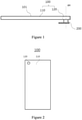
- FIG. 1 shows a schematic cross-sectional view of an under-screen camera assembly according to an example of the present application.
- the under-screen camera assembly includes an organic light-emitting diode display screen 100 (i.e., an OLED screen) and a camera module 200 located at a rear end of the organic light-emitting diode display screen 100.
- An optical axis ax of the camera module 200 is substantially perpendicular to a surface 101 of the organic light-emitting diode display screen 100.
- the "rear end” refers to an end of an imaging optical path of the camera module 200 close to an image side.
- the camera module 200 is located at a rear end of an under-screen camera area 120 of the organic light-emitting diode display screen 100.
- the under-screen camera area 120 is an area in the organic light-emitting diode display screen 100 that is adapted to the camera module 200.
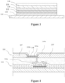
- Figure 2 shows a schematic top view of the organic light-emitting diode display screen in Figure 1 .
- a display area of the organic light-emitting diode display screen includes the under-screen camera area 120 and a non-under-screen camera area 110.
- the under-screen camera area 120 may be circular, and its size may be adapted to the size of the camera module 200.
- the under-screen camera area 120 may be surrounded by the non-under-screen camera area 110.
- the organic light-emitting diode display screen 100 adopts a special structure design to construct the under-screen camera area 120.
- the structure of the organic light-emitting diode display screen will be briefly described below.
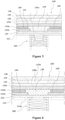
- FIG. 3 shows a schematic cross-sectional view of a typical organic light-emitting diode display screen.
- the organic light-emitting diode display screen 100 includes: a substrate 131, a buffer layer 132, a display layer 133 located above the buffer layer 132, and a packaging layer 134 covering the display layer 133, a polarizing layer 135 located above the packaging layer 134, and the cover plate 136 covering the polarizing layer 135.
- the display layer 133 can be further divided into a first electrode layer, a pixel layer, and a second electrode layer.
- the substrate may be a glass cover plate, or may be made of glass or transparent plastic.
- Transparent plastics can be an organic material selected from a group consisting of: polyethersulfone (PES), polyacrylate (PAR), polyetherimide (PEI), polyethylene naphthalate (PEN), polyethylene terephthalate (PET), polyphenylene sulfide (PPS), polyallylate, polyimide, polycarbonate (PC), cellulose triacetate (TAC) and/or cellulose acetate propionate (CAP).
- PES polyethersulfone
- PAR polyacrylate
- PEI polyetherimide
- PEN polyethylene naphthalate
- PET polyethylene terephthalate
- PPS polyphenylene sulfide
- PC polycarbonate
- TAC cellulose triacetate
- CAP cellulose acetate propionate
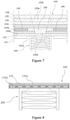
- the display layer 133 includes a first electrode 133b, a pixel layer 133a, and a second electrode 133c.
- the pixel layer 133a may include a plurality of pixel light-emitting structures 138 and a pixel defining structure 137 filling gaps between the plurality of pixel light-emitting structures 138.
- the pixel light-emitting structure 138 may include an electron injection layer, an electron transport layer, a light-emitting material layer, a hole transport layer, and a hole injection layer.
- the first electrode 133b and the second electrode 133c may cover the electron injection layer and the hole injection layer, respectively.
- the first electrode 133b is a metal cathode
- the second electrode 133c is an anode.
- the anode can be at least one material selected from a group consisting of: indium tin oxide (ITO), indium zinc oxide (IZO), zinc oxide (ZnO), indium oxide (In2O3), oxide indium gallium (IGO) and aluminum oxide zinc (AZO).
- Pixel electrodes all need to cover a surface of the light-emitting material, and the anode is transparent, and the first electrode 133b can be silver or silver alloy, so that the cathode is not transparent (it can also be coated with a reflective film to make the cathode to be not transparent), therefore, all the light emitted by the light-emitting layer material is transmitted from the anode, and a drain electrode of a thin film transistor is connected to the first electrode 133b so as to be conducted to the pixel light-emitting structure, and a signal for driving light emission is transmitted to the display layer of the OLED screen.
- the buffer layer 132 may be used as a barrier layer for reducing or preventing diffusion of impurity ions into the display layer 133, and reducing or preventing external air or moisture from penetrating therethrough.
- the buffer layer 132 can also flatten a surface of the substrate.
- the buffer layer usually also includes a TFT driving layer.
- the TFT driving layer has a plurality of TFT units (i.e., thin film transistors 132a) corresponding to the pixel light-emitting structure to drive the pixel light-emitting structure to emit light or be turned off (sometimes it can also drive the pixel light-emitting structure to change brightness).
- the thin film transistor 132a may be formed on a body material of the buffer layer, and its source electrode or drain electrode is connected to the first electrode 133b of the display layer.
- the packaging layer is a thin film packaging layer, which is located on the display layer.
- the thin film packaging layer can include an organic thin film and an inorganic thin film, or a plurality of organic films and inorganic films alternately stacked.
- a function of the thin film packaging layer is to prevent the display layer from being affected by external moisture or oxygen.
- the inorganic film stably blocks external moisture and oxygen, while the organic film can absorb the stress on the inorganic film to give the inorganic film flexibility.
- the polarizing layer includes a polarizer and a quarter-wave plate, which are used to reduce reflection of natural light and improve the contrast of the display screen.
- the polarizing layer also includes a touch control layer (or called the touch layer).
- FIG. 5 shows a schematic cross-sectional view of an under-screen camera assembly according to an example of the present application.
- the under-screen camera assembly includes an organic light-emitting diode display screen 100 and a camera module 200 located at a rear end of the organic light-emitting diode display screen 100.
- the organic light-emitting diode display screen 100 includes a substrate 131, a buffer layer 132, a first electrode layer 133b, a pixel layer 133a, a second electrode layer 133c, a packaging layer 134, a polarizing layer 135, and a cover plate 136 from bottom to top.
- the first electrode layer 133b, the pixel layer 133a, and the second electrode layer 133c may constitute a display layer 133.
- the pixel layer 133a may include a main display area 140 and a light-transmitting area 139.
- the shape and positional relationship of the main display area 140 and the light-transmitting area 139 can refer to Figure 2 .
- the main display area 140 corresponds to a non-under-screen camera area 110 in Figure 2
- the light-transmitting area 139 corresponds to the under-screen camera area 120 in Figure 2 .
- the polarizing layer 135 has a polarizing layer through hole 135a and the polarizing layer through hole 135a is located directly above the light-transmitting area 139.
- a light-passing channel based on the polarizing layer through hole 135a and the light-transmitting area 139 can constitute the under-screen camera area 120.
- An aperture of the polarizing layer through hole 135a may be 1 mm to 2.5 mm.
- the packaging layer 134 covers the main display area 140 and the light-transmitting area 139.
- the polarizing layer 135 can be bound to the packaging layer 134 by optical glue (the optical glue between the polarizing layer 135 and the packaging layer is not shown in Figure 5 ).
- the optical glue can also be used for bonding between the cover plate 136 and the polarizing layer 135 (the optical glue between the cover plate 136 and the polarizing layer 135 is not shown in Figure 5 ).
- the main display area 140 includes a plurality of pixel light-emitting structures 138 arranged in an array (it sould be noted that the pixel light-emitting structure 138 is not shown in the main display area 140 in Figure 5 , shape and position of the pixel light-emitting structure 138 can refer to Figure 4 ) and a pixel defining structure 137 filling gaps between the plurality of pixel light-emitting structures 138 (refer to Figure 4 ).
- each of the pixel light-emitting structures 138 includes a hole injection layer, a hole transport layer, an electron transport layer, an electron injection layer, and a light-emitting material layer located between the hole transport layer and the electron transport layer.
- the hole injection layer and the hole transport layer can be referred to as the hole layer
- the electron transport layer and the electron injection layer can be referred to as the electron layer.
- the light-transmitting area 139 may not be provided with the pixel light-emitting structure 138, but may be formed by filling with the optical glue. An light transmittance of the optical glue can reach 99%, and it has excellent light transmittance.
- the light-transmitting area 139 is also not provided with the pixel light-emitting structure, but different from the previous example, the light-transmitting area 139 in this example is made of a filling material of the pixel defining structure 137, or in other words, the light-transmitting area 139 in this example can be regarded as an ultra-large pixel defining structure, which can be compatible with the existing OLED manufacturing process to the greatest extent, so as to facilitate large-scale mass production, and help improve yield and reduce costs.
- the pixel defining structure can use a filling material with a relatively large light transmittance, the light-transmitting area 139 can meet requirement of the amount of light entering the under-screen camera module.
- a sidewall of the pixel defining structure 137 can be provided with a light blocking layer to better isolate each of the pixel light-emitting structures 138, and the filling material mentioned here is a filling material constituting a primary part of the pixel defining structure 137.
- the construction method of the light-transmitting area 139 of the present application is not limited to the above two examples.
- the light-transmitting area 139 is made of a material different from the main display area 140 (usually a light-transmitting material) or a light-transmitting structure (for example, a pixel light-emitting/defining structure with reduced pixel density), so that the light transmittance of the light-transmitting area 139 is greater than that of the main display area 140, and a light-transmitting area that is convenient for the under-screen camera module to receive external light can be obtained.
- the light-transmitting area 139 of the pixel layer 133a may not be subjected to special processing.
- the under-screen camera area can already meet the requirement of the amount of light entering the under-screen camera module, and at this time, the light-transmitting area 139 of the pixel layer 133a may not be subjected to special processing.
- the light-transmitting area 139 may have a pixel light-emitting structure 138, and its pixel size and spacing may be completely consistent with pixel size and spacing of the main display area 140, so as to provide a true full-screen display effect. Still referring to FIG.
- the packaging layer 134 packages the pixel layer 133a by covering an upper surface of the main display area 140 and the light-transmitting area 139 (it should be noted that, here "covering” is not limited to direct coverage, and other functional layers, such as a second electrode layer 133c, can be added between the packaging layer 134 and the pixel layer 133a, and the packaging layer 134 can achieve coverage of the upper surface of the main display area 140 and the light-transmitting area 139 by covering the second electrode layer 133c).
- This packaging method eliminates the need to punch a through hole in the display layer 133 (or the pixel layer 133a), and an inner wall of the through hole of the display layer 133 (or the pixel layer 133a) may not use a sidewall packaging layer 134 (or called a packaging material layer) to package. That is, an interface 141 between the light-transmitting area 139 and the main display area 140 may not be provided with the packaging material layer.
- a side surface of the main display area 140 and a side surface of the light-transmitting area 139 of the pixel layer 133a are in direct contact, and the two have the common interface 141.
- the light-transmitting area 139 When a structure of the light-transmitting area 139 is the same as that of the main display area 140, there may be no obvious interface 141 between the light-transmitting area 139 and the main display area 140 (that is, no packaging material may be added between the light-transmitting area 139 and the main display area 140, in particular, no packaging material for packaging a functional layer containing organic material is added between the light-transmitting area 139 and the main display area 140).
- the meaning of not providing the packaging material layer (or not using the packaging material to separate) between the light-transmitting area 139 and the main display area 140 can be understood as: there is a common interface 141 between the light-transmitting area 139 and the main display area 140 or there is no interface 141 between the light-transmitting area 139 and the main display area 140.
- the absence of the interface 141 between the light-transmitting area 139 and the main display area 140 can be understood as: there is a natural transition between the light-transmitting area 139 and the main display area 140, or the light-transmitting area 139 and the main display area 140 are continuous.
- the packaging material here can be understood as: a sealing material used to isolate the functional layer from the outside to prevent an organic material in the functional layer from oxidizing and degrading.
- the packaging layer 134 covering the upper surface of the light-transmitting area 139 and the main display area 140 is formed by using the packaging material.
- the pixel light-emitting structure 138 of the display layer 133 can be fabricated at a position closer to a central axis (or an optical axis) of the through hole, thereby reducing a blank area (i.e., an area without pixel) visible to users (such as mobile phone users).
- Figure 10 shows a schematic cross-sectional view of a comparative example of an organic light-emitting diode display screen using a through hole screen scheme.
- a through hole is punched in a display layer, and a sidewall of the through hole needs to cover a packaging layer 134b in order to avoid the oxidation of an organic material and cause product defects.
- a pixel light-emitting structure has to be arranged to a position further outside (that is, the side farther from the optical axis ax).
- the packaging layer 134b attached to the sidewall of the through hole runs vertically and is located in the through hole.
- the process complexity of manufacturing the packaging layer 134b in the through hole is higher than the traditional process complexity of manufacturing the packaging layer 134 on the surface of the display layer (or a second electrode layer).
- the packaging layer 134b in the through hole may have a problem of uneven thickness, and an edge area 134c of the packaging layer 134 on the surface close to the through hole may also have unevenness).
- the packaging layer 134b in the through hole may have a problem of uneven thickness, and an edge area 134c of the packaging layer 134 on the surface close to the through hole may also have unevenness.
- the radial direction can be regarded as a direction perpendicular to the optical axis
- this will cause the blank area (i.e., no pixel area) of the display layer to further increase.
- the light-transmitting area 139 is constructed in the display layer 133, the light-transmitting area 139 and the main display area 140 still form a complete integrity, and they may have a continuous surface for fabricating the second electrode layer 133c and the packaging layer 134 on the surface.
- the light-transmitting area 139 and the main display area 140 can constuct a continuous surface that can be attached by the packaging layer 134, so that the packaging layer 134 is still made by a traditional process (that is, the packaging layer is directly made on an upper surface of the semi-finished OLED), namely it can achieve the effect of preventing the oxidation of the organic material.
- this reduces the process difficulty of the "hole-dig screen", thereby improving the production efficiency and reducing the production cost of the under-screen camera module based on the "hole-dig screen”; on the other hand, it can ensure the amount of light entering the under-screen camera module, while it helps to reduce the size of the holes of the "hole-dig", thereby enhancing the user experience.
- the organic light-emitting diode display screens are not punched with through holes, and the light-passing channels of such display screens without through holes are analyzed as follows in combination with some specific data.
- transmittance of the glass cover 136 usually exceeds 90%
- transmittance of the optical glue is as high as 99%
- transmittance of the thin film packaging layer 134 also exceeds 90%
- transmittance of the second electrode layer 133c can reach 80%.
- the main portion of the buffer layer 132 can be arbitrarily stacked by inorganic materials and organic materials), overall transmittance of the light-passing channel of the display screen can exceed 67%, which meets a requirement of clear imaging, so that the front camera module becomes possible.
- the cover plate 136 may not be perforated, so as to achieve better protection and dust prevention. Since the transmittance of the cover plate can exceed 90%, the cover plate can still meet the imaging requirements of the under-screen module without perforating the cover plate.
- Figure 6 shows a schematic cross-sectional view of an under-screen camera assembly according to another example of the present application.
- the polarizing layer through hole 135a is filled with the optical glue 135b.
- the regional structure and materials of this example can be completely the same as the example of Figure 5 , and will not be repeated here.
- the substrate 131 has a substrate through hole 131a corresponding to the light-transmitting area 139. Digging the substrate (or called the base layer or base material) of the display device can help increase the amount of light entering the under-screen camera module.
- the main display area 140 and the light-transmitting area 139 of the pixel layer together form a continuous flat upper surface.
- the packaging layer packages the pixel layer by covering the continuous upper surface. In this way, in this example, there is no need to provide an packaging material between the main display area and the light-transmitting area to realize the packaging of the display layer, which reduces the process difficulty and also helps to reduce the aperture of the display blank area.
- Figure 7 shows a schematic cross-sectional view of an under-screen camera assembly according to yet another example of the present application.
- the display layer 133 in the organic light-emitting diode display screen 100, the display layer 133 includes a pixel layer 133a and a first electrode layer 133b and a second electrode layer 133c respectively located below and above the pixel layer 133a.
- a packaging layer 134 covers an upper surface of the second electrode layer 133c.
- the first electrode layer 133b located below constitutes a diaphragm (aperture diaphragm) of the camera module.
- Figure 7 shows a light-passing channel used for imaging in this example. It can be seen from Figure 7 that a through hole 133d of the first electrode layer 133b functions as a diaphragm.
- the substrate 131 has a substrate through hole 131a corresponding to the light-transmitting area 139, and a top end of the camera module 200 extends into the substrate through hole 131a and bears against a bottom surface of the buffer layer 132.
- the top of the under-screen camera module directly bears against the buffer layer 132 of the display device, which can reduce the transmission distance of external light to the camera module, thereby further increasing the amount of light entering the under-screen camera module.
- the light-passing channel is actually tapered, so under the premise that the size of the light through hole on the display surface (referring to the front surface) remains unchanged, the closer the top of the camera module is to the surface of display screen (referring to the front surface), the greater the amount of light received is. Conversely, under the premise of the same amount of light, the closer the top of the camera module is to the display surface (referring to the front surface), the more conducive to reducing the size of the light through hole (or called the aperture) on the surface of the display screen (referring to the front surface), thereby enhancing the user's visual experience.
- the first electrode layer is a cathode layer
- the cathode layer has a cathode layer through hole to form a light through hole of the diaphragm
- the thickness of the cathode layer reaches a thickness suitable for light shielding to form the light shielding portion of the diaphragm.
- the thickness of the first electrode can be increased to be sufficient to limit the size of the imaging light beam passing through the light-passing channel, and the first electrode can be made into a diaphragm.
- the diaphragm can also be formed by arranging an opaque material inside the first electrode of the light-passing channel.
- the first electrode layer has a first through hole to form an aperture of the diaphragm, and the first through hole is filled with the optical glue.
- Figure 8 shows a schematic cross-sectional view of an under-screen camera assembly of an example of the present application in which a light-transmitting area and a main display area adopt the same structure.
- the organic light-emitting diode display screen 100 includes: a substrate, a buffer layer, a first electrode layer, a pixel layer, a second electrode layer, a packaging layer, a polarizing layer 135 and a cover plate.
- the pixel layer includes a main display area and a light-transmitting area
- the polarizing layer 135 has a polarizing layer through hole 135a, and a part of the pixel layer 133a directly below the polarizing layer through hole 135a forms the light-transmitting area
- the packaging layer packages the pixel layer by covering an upper surface of the main display area and the light-transmitting area. No packaging material is used to separate the main display area and the light-transmitting area. In this example, there is no interface between the light-transmitting area and the main display area.
- the absence of tge interface between the light-transmitting area and the main display area can be understood as: a natural transition is between the light-transmitting area and the main display area, or the light-transmitting area and the main display area are continuous.
- the camera module 200 is installed at a rear end of the light-transmitting area (that is, a rear end of the polarizing layer through hole 135a).
- Figure 9 shows a schematic cross-sectional view of an under-screen camera assembly of another example of the present application inwhich a light-transmitting area and a main display area adopt a same structure.
- the substrate 131 has a substrate through hole 131a, a part of a bottom surface of the buffer layer 132 is exposed outside the substrate 131, and a top surface of the camera module 200 bears against the bottom surface of the buffer layer 132. (refers to the part of the bottom surface of the buffer layer 132 that is exposed to the outside of the substrate 131).
- the light-transmitting area may have a pixel light-emitting structure, and a pixel pitch of the light-transmitting area is greater than that of the main display area, so that a light transmittance of the light-transmitting area is greater than that of the main display area.
- the pixel density of the light-transmitting area sometimes referred to as PPI in the industry, and its full name is Pixels Per Inch
- the light transmittance of the light-transmitting area (corresponding to the under-screen camera area 120 shown in Figure 1 and Figure 2 ) is improved.
- the screen can avoid the imaging light path of the camera module without punching a hole, so that the display screen can be kept intact.
- the under-screen camera area 120 can perform image display.
- the under-screen camera area 120 and the non-under-screen camera area 110 can jointly form a complete picture, truly realizing a full-screen display effect.
- the under-screen camera assembly of this example is particularly suitable for use in smart phones, and the camera module in the under-screen camera assembly is particularly suitable for use as the front camera module of the smart phone.
- the under-screen camera assembly may further include: a first control unit, which is used to control both of the under-screen camera area and the non-under-screen camera area display images in the non-working state of the camera module; and in the working state of the camera module, to control the display function of the under-screen camera area to be turned off.
- a first control unit which is used to control both of the under-screen camera area and the non-under-screen camera area display images in the non-working state of the camera module; and in the working state of the camera module, to control the display function of the under-screen camera area to be turned off.
- the light-emitting layer of each pixel does not emit light, so that when the module is shooting, there will be no stray light from the display screen that affects the image shooting.
- all of the non-under-screen imaging area can display images; it is also possible to display no image in the surrounding area surrounding the under-screen camera area (that is, the light-emitting layer of the pixels in the surrounding area does not emit light), and the remaining part displays the image.
- the first control unit can turn off the display function of the under-screen camera area on the screen (that is, the under-screen camera area is not lit), so that external light can pass through the under-screen camera area and be received by the front camera. Since many improvements in the under-screen camera area can increase its light transmittance, the amount of light entering the front camera can reach the standard for effective imaging.
- the non-under-screen camera area can still work in order to display the picture taken by the front camera for better taking pictures (for example, when taking selfies, the non-under-screen camera area displays the face image) or shooting video (for example, during a video conference, the corresponding image is displayed by the non-under-screen camera area).
- the first control unit can be set in the operating system or application of the mobile phone (or other terminal device), or can be implemented as a part of the display driving circuit.
- the under-screen camera assembly may further include: a second control unit, which is used for compensating the brightness of the under-screen camera area when both of the under-screen camera area and the non-under-screen camera area display images.
- a second control unit which is used for compensating the brightness of the under-screen camera area when both of the under-screen camera area and the non-under-screen camera area display images.
- the pixel density of the under-screen camera area (sometimes referred to as PPI in the industry, and its full name is Pixels Per Inch) is set to be smaller than that of the non-under-screen camera area.
- the lower pixel density of the under-screen camera area is set to increase the pixel pitch.
- the light-emitting surface per unit area may be reduced, which may cause the brightness of the the under-screen camera area to be decreased (referring to the lower brightness of the under-screen camera area compared with the non-under-screen camera area).
- the brightness of the under-screen camera area is not compensated, then in the full-screen display, although the position of the front camera module can display images, its brightness may be significantly lower, then in contrast with the surrounding non-under-screen camera area, this position (the position of the front camera module) may form a dark spot (that is, a block whose brightness is significantly lower than the surrounding area). Such dark spots may be easily noticed by users visually, thereby affecting user experience.
- the compensation for the brightness may be compensation at the software level, for example, adaptive adjustment at the operating system level or application level of the mobile phone (or other terminal device). For example, through software adjustment, the brightness of the under-screen camera area is increased, so as to be consistent with the surrounding non-under-screen camera area, thereby eliminating or suppressing dark spots in the under-screen camera area. In this way, the user can see a complete screen and the complete and continuous image displayed on the screen, and obtain an extremely shocking visual enjoyment.
- the brightness of the under-screen camera area can also be compensated in the display driving circuit.
- the TFT i.e., the thin film transistor switch under the light-emitting layer of each pixel
- the second control unit can be implemented at the hardware level of the display screen.
- the under-screen camera assembly further includes a second control unit, which is used to compensate display parameters of the under-screen camera area when both of the under-screen camera area and the non-under-screen camera area display images, so that the displayed image transitions smoothly between the under-screen camera area and the non-under-screen camera area, so that the under-screen camera area and the non-under-screen camera area can form a complete and continuous picture, and there is no boundary between the under-screen camera area and the non-under-screen camera area in the picture that is easy to be noticed by the naked eye.
- Compensating the display parameters of the under-screen camera area may be compensation at the software level, such as adaptive adjustment at the operating system level or application level of a mobile phone (or other terminal device).
- the display driving circuit can also be used to compensate the display parameters of the under-screen camera area.
- Display parameters can include brightness and contrast.
- the pixel size of the under-screen camera area and the pixel size of the non-under-screen camera area may be the same.
- the pixel size here refers to the size of the light-emitting structure.
- the under-screen camera area and the non-under-screen camera area can share many production processes and production equipment, which helps to improve production efficiency and increase yield.
- the pixel size of the under-screen camera area and the pixel size of the non-under-screen camera area may also be different. Reducing the pixel density of the under-screen camera area can help increase the spacing between pixels, thereby increasing the transmittance of the under-screen camera area.
- Figure 11 shows a schematic diagram of a substrate of an OLED screen with a positioning mark.
- at least two positioning marks 150 may be provided on the substrate of the OLED screen, and the positioning marks 150 are used for position identification during the assembly process of the OLED screen and the camera module to improve the assembly accuracy (for example, improve the alignment accuracy of the through-light hole).
- the positioning mark does not overlap with the projection of the camera module on the display screen, so that the camera module and the display screen can be adjusted in real time during assembly.
- glue material can be set on the contact surface for bonding and fixing, or the camera module can be closely attached to the OLED screen and bonded by glue on the side, or two places (contact surface and side surface) can be bonded at the same time.
- the positioning mark can be an ink pattern, or it can be realized by laser marking, or it can be formed by grooving the substrate of the OLED screen, or it can be a special structure integrally formed with the substrate.
- a terminal device which includes the under-screen camera assembly described in any of the foregoing examples.
- the camera module may be used as a front camera module of the terminal device, and the organic light-emitting diode display screen may be used as a display panel on the front of the terminal device.
- pixel density herein is sometimes also referred to as display density.
Landscapes
- Engineering & Computer Science (AREA)
- Signal Processing (AREA)
- Physics & Mathematics (AREA)
- Multimedia (AREA)
- Microelectronics & Electronic Packaging (AREA)
- Optics & Photonics (AREA)
- Geometry (AREA)
- Electroluminescent Light Sources (AREA)
- Devices For Indicating Variable Information By Combining Individual Elements (AREA)
Applications Claiming Priority (2)
| Application Number | Priority Date | Filing Date | Title |
|---|---|---|---|
| CN201910339111.8A CN111863868B (zh) | 2019-04-25 | 2019-04-25 | 屏下摄像组件及相应的有机发光二极管显示屏和终端设备 |
| PCT/CN2020/076566 WO2020215879A1 (zh) | 2019-04-25 | 2020-02-25 | 屏下摄像组件及相应的有机发光二极管显示屏和终端设备 |
Publications (2)
| Publication Number | Publication Date |
|---|---|
| EP3962045A1 true EP3962045A1 (de) | 2022-03-02 |
| EP3962045A4 EP3962045A4 (de) | 2022-05-25 |
Family
ID=72941337
Family Applications (1)
| Application Number | Title | Priority Date | Filing Date |
|---|---|---|---|
| EP20794749.0A Pending EP3962045A4 (de) | 2019-04-25 | 2020-02-25 | Fotografieranordnung unter einem bildschirm sowie entsprechender organischer leuchtdiodenanzeigeschirm und endgerät |
Country Status (4)
| Country | Link |
|---|---|
| US (1) | US20220208897A1 (de) |
| EP (1) | EP3962045A4 (de) |
| CN (1) | CN111863868B (de) |
| WO (1) | WO2020215879A1 (de) |
Families Citing this family (26)
| Publication number | Priority date | Publication date | Assignee | Title |
|---|---|---|---|---|
| CN111276048B (zh) * | 2019-06-14 | 2022-10-28 | 荣耀终端有限公司 | 一种显示屏和电子设备 |
| CN211743161U (zh) * | 2020-04-24 | 2020-10-23 | 京东方科技集团股份有限公司 | 一种显示基板和显示装置 |
| CN116157763A (zh) * | 2020-07-21 | 2023-05-23 | 三星电子株式会社 | 包括显示器和相机装置的电子装置 |
| CN114068620B (zh) * | 2020-07-31 | 2025-07-18 | 京东方科技集团股份有限公司 | 一种显示装置 |
| CN112037657B (zh) * | 2020-09-14 | 2022-12-02 | 京东方科技集团股份有限公司 | 封装结构及其制备方法、显示面板、显示装置 |
| CN114464752A (zh) * | 2020-11-09 | 2022-05-10 | 上海和辉光电股份有限公司 | Oled面板及其点胶方法 |
| CN112531127B (zh) * | 2020-11-24 | 2023-05-30 | 上海和辉光电股份有限公司 | 一种有机电致发光显示面板及其制备方法 |
| CN114649493B (zh) * | 2020-12-21 | 2025-05-09 | 华为技术有限公司 | 显示组件及其制备方法、显示装置 |
| CN114845009A (zh) * | 2021-02-02 | 2022-08-02 | 北京小米移动软件有限公司 | 摄像头模组及其控制方法、装置、存储介质、电子设备 |
| CN112820767A (zh) * | 2021-02-22 | 2021-05-18 | 武汉华星光电半导体显示技术有限公司 | 显示装置和电子设备 |
| CN113421912B (zh) * | 2021-06-28 | 2022-08-23 | 武汉华星光电半导体显示技术有限公司 | 有机发光显示装置及其制作方法 |
| CN113777687B (zh) * | 2021-08-12 | 2023-04-18 | 惠州Tcl云创科技有限公司 | 一种屏下摄像头组件、背光模组及显示设备 |
| CN114241903A (zh) * | 2021-09-30 | 2022-03-25 | 华为技术有限公司 | 显示面板、电子设备及显示面板的制作方法 |
| US12426448B2 (en) | 2021-11-24 | 2025-09-23 | Wuhan China Star Optoelectronics Semiconductor Display Technology Co., Ltd. | Display module and manufacturing method of display module |
| CN114141833B (zh) * | 2021-11-24 | 2023-12-01 | 武汉华星光电半导体显示技术有限公司 | 显示模组及显示模组的制备方法 |
| KR20230094334A (ko) * | 2021-12-21 | 2023-06-28 | 엘지디스플레이 주식회사 | 표시 장치 |
| CN116453425B (zh) * | 2022-01-04 | 2025-10-31 | 北京小米移动软件有限公司 | 一种屏幕及屏下摄像头的摄像方法 |
| CN114415411B (zh) * | 2022-01-28 | 2024-03-26 | 武汉华星光电技术有限公司 | 屏下监测显示装置 |
| CN114567718B (zh) * | 2022-03-02 | 2023-08-18 | 联想(北京)有限公司 | 电子设备 |
| CN114740552B (zh) * | 2022-04-20 | 2023-05-30 | 武汉华星光电半导体显示技术有限公司 | 显示模组及显示装置 |
| CN115241256B (zh) * | 2022-07-29 | 2026-01-13 | Oppo广东移动通信有限公司 | 显示装置、显示方法及电子设备 |
| CN116030720B (zh) * | 2022-12-30 | 2026-04-14 | 联想(北京)有限公司 | 显示装置、显示装置的安装方法及电子设备 |
| CN117119828B (zh) * | 2023-02-16 | 2025-04-04 | 荣耀终端股份有限公司 | 显示屏及电子设备 |
| US12510804B1 (en) * | 2024-11-14 | 2025-12-30 | Liqxtal Technology Inc. | Optical system having pixel-based diaphragm |
| CN119811208A (zh) * | 2025-01-22 | 2025-04-11 | 合肥维信诺科技有限公司 | 显示模组及其组合方法、显示装置 |
| CN120076659B (zh) * | 2025-02-27 | 2026-04-24 | 昆山国显光电有限公司 | 显示模组及其制备方法和显示装置 |
Family Cites Families (27)
| Publication number | Priority date | Publication date | Assignee | Title |
|---|---|---|---|---|
| US6822709B1 (en) * | 2003-09-23 | 2004-11-23 | Toppoly Optoelectronics Corp. | Transflective display device |
| JP2009520457A (ja) * | 2005-12-20 | 2009-05-21 | コーニンクレッカ フィリップス エレクトロニクス エヌ ヴィ | 誘電体高分子アクチュエータを用いたカメラダイアフラムおよびレンズ位置決めシステム |
| US7535163B2 (en) * | 2006-02-22 | 2009-05-19 | Tpo Displays Corp. | System for displaying images including electroluminescent device and method for fabricating the same |
| CN104362169B (zh) * | 2014-11-26 | 2017-10-10 | 京东方科技集团股份有限公司 | 一种有机发光二极管阵列基板及其制备方法、显示装置 |
| KR20160076034A (ko) * | 2014-12-22 | 2016-06-30 | 삼성디스플레이 주식회사 | 유기 발광 표시 장치 및 유기 발광 표시 장치의 제조 방법 |
| KR102465080B1 (ko) * | 2015-08-24 | 2022-11-10 | 엘지디스플레이 주식회사 | 표시장치 및 표시패널 |
| KR102790344B1 (ko) * | 2016-12-29 | 2025-04-01 | 엘지디스플레이 주식회사 | 검사장치 및 이를 이용한 검사방법 |
| CN207251757U (zh) * | 2017-04-07 | 2018-04-17 | 宁波舜宇光电信息有限公司 | 摄像装置及其模制封装组件以及电子设备 |
| EP3982618B1 (de) * | 2017-04-25 | 2023-03-15 | Huawei Technologies Co., Ltd. | Elektronische vorrichtung mit lcd-anzeige |
| CN107024835B (zh) * | 2017-05-12 | 2020-07-28 | 京东方科技集团股份有限公司 | 光刻胶组合物及其制备方法、oled阵列基板及其制备方法 |
| WO2018216545A1 (ja) * | 2017-05-22 | 2018-11-29 | シャープ株式会社 | 表示デバイス |
| WO2019047126A1 (zh) * | 2017-09-07 | 2019-03-14 | 华为技术有限公司 | 一种有机发光显示oled屏幕及终端 |
| GB2566936A (en) * | 2017-09-20 | 2019-04-03 | Flexenable Ltd | Display device |
| CN108365122A (zh) * | 2017-09-30 | 2018-08-03 | 云谷(固安)科技有限公司 | 显示屏以及电子设备 |
| CN107946341B (zh) * | 2017-11-10 | 2020-05-22 | 上海天马微电子有限公司 | 显示装置和显示装置的制造方法 |
| KR102664717B1 (ko) * | 2018-04-13 | 2024-05-10 | 삼성전자 주식회사 | 표시 영역에 의해 둘러싸인 홀 영역을 우회하는 복수의 배선들을 포함하는 디스플레이 및 이를 포함하는 전자 장치 |
| CN108461532A (zh) * | 2018-05-28 | 2018-08-28 | 信利光电股份有限公司 | 一种oled显示屏模组、制作方法及移动终端 |
| CN109376570B (zh) * | 2018-07-09 | 2024-06-04 | 东莞市美光达光学科技有限公司 | 一种用于屏下指纹识别模组的微型补光照明系统 |
| CN109037293B (zh) * | 2018-08-01 | 2021-08-31 | 京东方科技集团股份有限公司 | 显示面板及其制作方法、显示装置 |
| CN109120753B (zh) * | 2018-08-21 | 2021-01-26 | 武汉天马微电子有限公司 | 一种显示面板及显示装置 |
| CN109068044B (zh) * | 2018-09-28 | 2023-11-03 | 武汉华星光电技术有限公司 | 光学组件以及显示装置 |
| CN109545099B (zh) * | 2018-11-22 | 2020-06-16 | 武汉华星光电技术有限公司 | 一种液晶显示面板及其终端装置 |
| US10879499B2 (en) * | 2018-12-03 | 2020-12-29 | Wuhan China Star Optoelectronics Semiconductor Display Technology Co., Ltd. | Display module, manufacturing method thereof and electronic device |
| CN109495622A (zh) * | 2018-12-28 | 2019-03-19 | Oppo广东移动通信有限公司 | 保护盖板、壳组件和移动终端 |
| CN111384269B (zh) * | 2018-12-29 | 2021-08-03 | Tcl科技集团股份有限公司 | 量子点发光二极管及其制备方法 |
| KR102830391B1 (ko) * | 2019-03-12 | 2025-07-07 | 삼성디스플레이 주식회사 | 표시 장치 및 이의 제조 방법 |
| CN110875369A (zh) * | 2019-11-27 | 2020-03-10 | 京东方科技集团股份有限公司 | 显示背板、显示面板及其制作方法和显示装置 |
-
2019
- 2019-04-25 CN CN201910339111.8A patent/CN111863868B/zh active Active
-
2020
- 2020-02-25 WO PCT/CN2020/076566 patent/WO2020215879A1/zh not_active Ceased
- 2020-02-25 EP EP20794749.0A patent/EP3962045A4/de active Pending
- 2020-02-25 US US17/606,136 patent/US20220208897A1/en active Pending
Also Published As
| Publication number | Publication date |
|---|---|
| US20220208897A1 (en) | 2022-06-30 |
| CN111863868B (zh) | 2023-01-13 |
| WO2020215879A1 (zh) | 2020-10-29 |
| CN111863868A (zh) | 2020-10-30 |
| EP3962045A4 (de) | 2022-05-25 |
Similar Documents
| Publication | Publication Date | Title |
|---|---|---|
| EP3962045A1 (de) | Fotografieranordnung unter einem bildschirm sowie entsprechender organischer leuchtdiodenanzeigeschirm und endgerät | |
| US11271053B2 (en) | Display panel having one display region surrounding another display regiion and display device having the same | |
| US10761386B2 (en) | Display panel and display device | |
| US11335750B2 (en) | Organic light emitting diode (OLED) display panel and OLED display device | |
| KR102554160B1 (ko) | 디스플레이 패널 및 단말기 | |
| US20190331960A1 (en) | Display apparatus | |
| US8823668B2 (en) | Liquid crystal device | |
| US11022828B2 (en) | Display device and fabrication method thereof | |
| EP3156841A1 (de) | Anzeigebasisplatte, anzeigetafel und anzeigevorrichtung | |
| RU2736269C1 (ru) | Экран терминала, способ управления экраном терминала и терминал | |
| WO2020215878A1 (zh) | 屏下摄像组件及相应的有机发光二极管显示屏和终端设备 | |
| EP3952260B1 (de) | Kameraanordnung unter der anzeige und entsprechendes endgerät | |
| WO2013187281A1 (ja) | 表示装置 | |
| US11409106B2 (en) | Display module and head-mounted display device including the same | |
| KR20170071064A (ko) | 광 제어 장치, 그를 포함한 투명표시장치, 및 그의 제조방법 | |
| KR102756972B1 (ko) | 표시장치와 그 픽셀 어레이 기판 | |
| US20140168574A1 (en) | Liquid crystal display device | |
| US12161011B2 (en) | Display device and method of providing the same | |
| KR102944680B1 (ko) | 표시 장치와 그의 제조 방법 | |
| KR20190072134A (ko) | 디스플레이 장치 | |
| US12075150B2 (en) | Under-screen camera assembly and corresponding terminal device | |
| CN210123986U (zh) | 终端屏幕及终端 | |
| US7751116B2 (en) | Flexible display | |
| US20230061355A1 (en) | Display apparatus and method of manufacturing the same | |
| US20250216739A1 (en) | Light Controlling Panel and Transparent Display Device Including the Same |
Legal Events
| Date | Code | Title | Description |
|---|---|---|---|
| STAA | Information on the status of an ep patent application or granted ep patent |
Free format text: STATUS: THE INTERNATIONAL PUBLICATION HAS BEEN MADE |
|
| PUAI | Public reference made under article 153(3) epc to a published international application that has entered the european phase |
Free format text: ORIGINAL CODE: 0009012 |
|
| STAA | Information on the status of an ep patent application or granted ep patent |
Free format text: STATUS: REQUEST FOR EXAMINATION WAS MADE |
|
| 17P | Request for examination filed |
Effective date: 20211119 |
|
| AK | Designated contracting states |
Kind code of ref document: A1 Designated state(s): AL AT BE BG CH CY CZ DE DK EE ES FI FR GB GR HR HU IE IS IT LI LT LU LV MC MK MT NL NO PL PT RO RS SE SI SK SM TR |
|
| A4 | Supplementary search report drawn up and despatched |
Effective date: 20220426 |
|
| RIC1 | Information provided on ipc code assigned before grant |
Ipc: H01L 51/52 20060101ALI20220420BHEP Ipc: H01L 27/32 20060101ALI20220420BHEP Ipc: H04N 5/225 20060101ALI20220420BHEP Ipc: H04M 1/02 20060101AFI20220420BHEP |
|
| DAV | Request for validation of the european patent (deleted) | ||
| DAX | Request for extension of the european patent (deleted) | ||
| P01 | Opt-out of the competence of the unified patent court (upc) registered |
Effective date: 20230524 |
|
| STAA | Information on the status of an ep patent application or granted ep patent |
Free format text: STATUS: EXAMINATION IS IN PROGRESS |
|
| 17Q | First examination report despatched |
Effective date: 20240924 |