EP3926404B1 - Messvorrichtung und messverfahren, expositionseinrichtung und expositionsverfahren und vorrichtungsherstellungsverfahren - Google Patents
Messvorrichtung und messverfahren, expositionseinrichtung und expositionsverfahren und vorrichtungsherstellungsverfahren Download PDFInfo
- Publication number
- EP3926404B1 EP3926404B1 EP21177718.0A EP21177718A EP3926404B1 EP 3926404 B1 EP3926404 B1 EP 3926404B1 EP 21177718 A EP21177718 A EP 21177718A EP 3926404 B1 EP3926404 B1 EP 3926404B1
- Authority
- EP
- European Patent Office
- Prior art keywords
- measurement
- grating
- grating mark
- objective optical
- mark
- Prior art date
- Legal status (The legal status is an assumption and is not a legal conclusion. Google has not performed a legal analysis and makes no representation as to the accuracy of the status listed.)
- Active
Links
Images





Classifications
-
- G—PHYSICS
- G03—PHOTOGRAPHY; CINEMATOGRAPHY; ANALOGOUS TECHNIQUES USING WAVES OTHER THAN OPTICAL WAVES; ELECTROGRAPHY; HOLOGRAPHY
- G03F—PHOTOMECHANICAL PRODUCTION OF TEXTURED OR PATTERNED SURFACES, e.g. FOR PRINTING, FOR PROCESSING OF SEMICONDUCTOR DEVICES; MATERIALS THEREFOR; ORIGINALS THEREFOR; APPARATUS SPECIALLY ADAPTED THEREFOR
- G03F7/00—Photomechanical, e.g. photolithographic, production of textured or patterned surfaces, e.g. printing surfaces; Materials therefor, e.g. comprising photoresists; Apparatus specially adapted therefor
- G03F7/70—Microphotolithographic exposure; Apparatus therefor
- G03F7/70483—Information management; Active and passive control; Testing; Wafer monitoring, e.g. pattern monitoring
- G03F7/70605—Workpiece metrology
- G03F7/70681—Metrology strategies
- G03F7/70683—Mark designs
-
- G—PHYSICS
- G01—MEASURING; TESTING
- G01B—MEASURING LENGTH, THICKNESS OR SIMILAR LINEAR DIMENSIONS; MEASURING ANGLES; MEASURING AREAS; MEASURING IRREGULARITIES OF SURFACES OR CONTOURS
- G01B11/00—Measuring arrangements characterised by the use of optical techniques
-
- G—PHYSICS
- G01—MEASURING; TESTING
- G01B—MEASURING LENGTH, THICKNESS OR SIMILAR LINEAR DIMENSIONS; MEASURING ANGLES; MEASURING AREAS; MEASURING IRREGULARITIES OF SURFACES OR CONTOURS
- G01B11/00—Measuring arrangements characterised by the use of optical techniques
- G01B11/14—Measuring arrangements characterised by the use of optical techniques for measuring distance or clearance between spaced objects or spaced apertures
-
- G—PHYSICS
- G01—MEASURING; TESTING
- G01D—MEASURING NOT SPECIALLY ADAPTED FOR A SPECIFIC VARIABLE; ARRANGEMENTS FOR MEASURING TWO OR MORE VARIABLES NOT COVERED IN A SINGLE OTHER SUBCLASS; TARIFF METERING APPARATUS; MEASURING OR TESTING NOT OTHERWISE PROVIDED FOR
- G01D5/00—Mechanical means for transferring the output of a sensing member; Means for converting the output of a sensing member to another variable where the form or nature of the sensing member does not constrain the means for converting; Transducers not specially adapted for a specific variable
- G01D5/26—Mechanical means for transferring the output of a sensing member; Means for converting the output of a sensing member to another variable where the form or nature of the sensing member does not constrain the means for converting; Transducers not specially adapted for a specific variable characterised by optical transfer means, i.e. using infrared, visible, or ultraviolet light
- G01D5/32—Mechanical means for transferring the output of a sensing member; Means for converting the output of a sensing member to another variable where the form or nature of the sensing member does not constrain the means for converting; Transducers not specially adapted for a specific variable characterised by optical transfer means, i.e. using infrared, visible, or ultraviolet light with attenuation or whole or partial obturation of beams of light
- G01D5/34—Mechanical means for transferring the output of a sensing member; Means for converting the output of a sensing member to another variable where the form or nature of the sensing member does not constrain the means for converting; Transducers not specially adapted for a specific variable characterised by optical transfer means, i.e. using infrared, visible, or ultraviolet light with attenuation or whole or partial obturation of beams of light the beams of light being detected by photocells
- G01D5/36—Forming the light into pulses
- G01D5/38—Forming the light into pulses by diffraction gratings
-
- G—PHYSICS
- G03—PHOTOGRAPHY; CINEMATOGRAPHY; ANALOGOUS TECHNIQUES USING WAVES OTHER THAN OPTICAL WAVES; ELECTROGRAPHY; HOLOGRAPHY
- G03F—PHOTOMECHANICAL PRODUCTION OF TEXTURED OR PATTERNED SURFACES, e.g. FOR PRINTING, FOR PROCESSING OF SEMICONDUCTOR DEVICES; MATERIALS THEREFOR; ORIGINALS THEREFOR; APPARATUS SPECIALLY ADAPTED THEREFOR
- G03F7/00—Photomechanical, e.g. photolithographic, production of textured or patterned surfaces, e.g. printing surfaces; Materials therefor, e.g. comprising photoresists; Apparatus specially adapted therefor
- G03F7/20—Exposure; Apparatus therefor
-
- G—PHYSICS
- G03—PHOTOGRAPHY; CINEMATOGRAPHY; ANALOGOUS TECHNIQUES USING WAVES OTHER THAN OPTICAL WAVES; ELECTROGRAPHY; HOLOGRAPHY
- G03F—PHOTOMECHANICAL PRODUCTION OF TEXTURED OR PATTERNED SURFACES, e.g. FOR PRINTING, FOR PROCESSING OF SEMICONDUCTOR DEVICES; MATERIALS THEREFOR; ORIGINALS THEREFOR; APPARATUS SPECIALLY ADAPTED THEREFOR
- G03F7/00—Photomechanical, e.g. photolithographic, production of textured or patterned surfaces, e.g. printing surfaces; Materials therefor, e.g. comprising photoresists; Apparatus specially adapted therefor
- G03F7/70—Microphotolithographic exposure; Apparatus therefor
- G03F7/70058—Mask illumination systems
- G03F7/7015—Details of optical elements
- G03F7/70158—Diffractive optical elements
-
- G—PHYSICS
- G03—PHOTOGRAPHY; CINEMATOGRAPHY; ANALOGOUS TECHNIQUES USING WAVES OTHER THAN OPTICAL WAVES; ELECTROGRAPHY; HOLOGRAPHY
- G03F—PHOTOMECHANICAL PRODUCTION OF TEXTURED OR PATTERNED SURFACES, e.g. FOR PRINTING, FOR PROCESSING OF SEMICONDUCTOR DEVICES; MATERIALS THEREFOR; ORIGINALS THEREFOR; APPARATUS SPECIALLY ADAPTED THEREFOR
- G03F7/00—Photomechanical, e.g. photolithographic, production of textured or patterned surfaces, e.g. printing surfaces; Materials therefor, e.g. comprising photoresists; Apparatus specially adapted therefor
- G03F7/70—Microphotolithographic exposure; Apparatus therefor
- G03F7/70216—Mask projection systems
- G03F7/70241—Optical aspects of refractive lens systems, i.e. comprising only refractive elements
-
- G—PHYSICS
- G03—PHOTOGRAPHY; CINEMATOGRAPHY; ANALOGOUS TECHNIQUES USING WAVES OTHER THAN OPTICAL WAVES; ELECTROGRAPHY; HOLOGRAPHY
- G03F—PHOTOMECHANICAL PRODUCTION OF TEXTURED OR PATTERNED SURFACES, e.g. FOR PRINTING, FOR PROCESSING OF SEMICONDUCTOR DEVICES; MATERIALS THEREFOR; ORIGINALS THEREFOR; APPARATUS SPECIALLY ADAPTED THEREFOR
- G03F7/00—Photomechanical, e.g. photolithographic, production of textured or patterned surfaces, e.g. printing surfaces; Materials therefor, e.g. comprising photoresists; Apparatus specially adapted therefor
- G03F7/70—Microphotolithographic exposure; Apparatus therefor
- G03F7/70216—Mask projection systems
- G03F7/70258—Projection system adjustments, e.g. adjustments during exposure or alignment during assembly of projection system
-
- G—PHYSICS
- G03—PHOTOGRAPHY; CINEMATOGRAPHY; ANALOGOUS TECHNIQUES USING WAVES OTHER THAN OPTICAL WAVES; ELECTROGRAPHY; HOLOGRAPHY
- G03F—PHOTOMECHANICAL PRODUCTION OF TEXTURED OR PATTERNED SURFACES, e.g. FOR PRINTING, FOR PROCESSING OF SEMICONDUCTOR DEVICES; MATERIALS THEREFOR; ORIGINALS THEREFOR; APPARATUS SPECIALLY ADAPTED THEREFOR
- G03F7/00—Photomechanical, e.g. photolithographic, production of textured or patterned surfaces, e.g. printing surfaces; Materials therefor, e.g. comprising photoresists; Apparatus specially adapted therefor
- G03F7/70—Microphotolithographic exposure; Apparatus therefor
- G03F7/70483—Information management; Active and passive control; Testing; Wafer monitoring, e.g. pattern monitoring
- G03F7/70605—Workpiece metrology
- G03F7/706835—Metrology information management or control
-
- G—PHYSICS
- G03—PHOTOGRAPHY; CINEMATOGRAPHY; ANALOGOUS TECHNIQUES USING WAVES OTHER THAN OPTICAL WAVES; ELECTROGRAPHY; HOLOGRAPHY
- G03F—PHOTOMECHANICAL PRODUCTION OF TEXTURED OR PATTERNED SURFACES, e.g. FOR PRINTING, FOR PROCESSING OF SEMICONDUCTOR DEVICES; MATERIALS THEREFOR; ORIGINALS THEREFOR; APPARATUS SPECIALLY ADAPTED THEREFOR
- G03F7/00—Photomechanical, e.g. photolithographic, production of textured or patterned surfaces, e.g. printing surfaces; Materials therefor, e.g. comprising photoresists; Apparatus specially adapted therefor
- G03F7/70—Microphotolithographic exposure; Apparatus therefor
- G03F7/70483—Information management; Active and passive control; Testing; Wafer monitoring, e.g. pattern monitoring
- G03F7/70605—Workpiece metrology
- G03F7/706843—Metrology apparatus
- G03F7/706845—Calibration, e.g. tool-to-tool calibration, beam alignment, spot position or focus
-
- G—PHYSICS
- G03—PHOTOGRAPHY; CINEMATOGRAPHY; ANALOGOUS TECHNIQUES USING WAVES OTHER THAN OPTICAL WAVES; ELECTROGRAPHY; HOLOGRAPHY
- G03F—PHOTOMECHANICAL PRODUCTION OF TEXTURED OR PATTERNED SURFACES, e.g. FOR PRINTING, FOR PROCESSING OF SEMICONDUCTOR DEVICES; MATERIALS THEREFOR; ORIGINALS THEREFOR; APPARATUS SPECIALLY ADAPTED THEREFOR
- G03F7/00—Photomechanical, e.g. photolithographic, production of textured or patterned surfaces, e.g. printing surfaces; Materials therefor, e.g. comprising photoresists; Apparatus specially adapted therefor
- G03F7/70—Microphotolithographic exposure; Apparatus therefor
- G03F7/70483—Information management; Active and passive control; Testing; Wafer monitoring, e.g. pattern monitoring
- G03F7/70605—Workpiece metrology
- G03F7/706843—Metrology apparatus
- G03F7/706849—Irradiation branch, e.g. optical system details, illumination mode or polarisation control
-
- G—PHYSICS
- G03—PHOTOGRAPHY; CINEMATOGRAPHY; ANALOGOUS TECHNIQUES USING WAVES OTHER THAN OPTICAL WAVES; ELECTROGRAPHY; HOLOGRAPHY
- G03F—PHOTOMECHANICAL PRODUCTION OF TEXTURED OR PATTERNED SURFACES, e.g. FOR PRINTING, FOR PROCESSING OF SEMICONDUCTOR DEVICES; MATERIALS THEREFOR; ORIGINALS THEREFOR; APPARATUS SPECIALLY ADAPTED THEREFOR
- G03F7/00—Photomechanical, e.g. photolithographic, production of textured or patterned surfaces, e.g. printing surfaces; Materials therefor, e.g. comprising photoresists; Apparatus specially adapted therefor
- G03F7/70—Microphotolithographic exposure; Apparatus therefor
- G03F7/70483—Information management; Active and passive control; Testing; Wafer monitoring, e.g. pattern monitoring
- G03F7/70605—Workpiece metrology
- G03F7/706843—Metrology apparatus
- G03F7/706851—Detection branch, e.g. detector arrangements, polarisation control, wavelength control or dark/bright field detection
-
- G—PHYSICS
- G03—PHOTOGRAPHY; CINEMATOGRAPHY; ANALOGOUS TECHNIQUES USING WAVES OTHER THAN OPTICAL WAVES; ELECTROGRAPHY; HOLOGRAPHY
- G03F—PHOTOMECHANICAL PRODUCTION OF TEXTURED OR PATTERNED SURFACES, e.g. FOR PRINTING, FOR PROCESSING OF SEMICONDUCTOR DEVICES; MATERIALS THEREFOR; ORIGINALS THEREFOR; APPARATUS SPECIALLY ADAPTED THEREFOR
- G03F7/00—Photomechanical, e.g. photolithographic, production of textured or patterned surfaces, e.g. printing surfaces; Materials therefor, e.g. comprising photoresists; Apparatus specially adapted therefor
- G03F7/70—Microphotolithographic exposure; Apparatus therefor
- G03F7/70691—Handling of masks or workpieces
- G03F7/70775—Position control, e.g. interferometers or encoders for determining the stage position
-
- G—PHYSICS
- G03—PHOTOGRAPHY; CINEMATOGRAPHY; ANALOGOUS TECHNIQUES USING WAVES OTHER THAN OPTICAL WAVES; ELECTROGRAPHY; HOLOGRAPHY
- G03F—PHOTOMECHANICAL PRODUCTION OF TEXTURED OR PATTERNED SURFACES, e.g. FOR PRINTING, FOR PROCESSING OF SEMICONDUCTOR DEVICES; MATERIALS THEREFOR; ORIGINALS THEREFOR; APPARATUS SPECIALLY ADAPTED THEREFOR
- G03F9/00—Registration or positioning of originals, masks, frames, photographic sheets or textured or patterned surfaces, e.g. automatically
-
- G—PHYSICS
- G03—PHOTOGRAPHY; CINEMATOGRAPHY; ANALOGOUS TECHNIQUES USING WAVES OTHER THAN OPTICAL WAVES; ELECTROGRAPHY; HOLOGRAPHY
- G03F—PHOTOMECHANICAL PRODUCTION OF TEXTURED OR PATTERNED SURFACES, e.g. FOR PRINTING, FOR PROCESSING OF SEMICONDUCTOR DEVICES; MATERIALS THEREFOR; ORIGINALS THEREFOR; APPARATUS SPECIALLY ADAPTED THEREFOR
- G03F9/00—Registration or positioning of originals, masks, frames, photographic sheets or textured or patterned surfaces, e.g. automatically
- G03F9/70—Registration or positioning of originals, masks, frames, photographic sheets or textured or patterned surfaces, e.g. automatically for microlithography
- G03F9/7003—Alignment type or strategy, e.g. leveling, global alignment
-
- G—PHYSICS
- G03—PHOTOGRAPHY; CINEMATOGRAPHY; ANALOGOUS TECHNIQUES USING WAVES OTHER THAN OPTICAL WAVES; ELECTROGRAPHY; HOLOGRAPHY
- G03F—PHOTOMECHANICAL PRODUCTION OF TEXTURED OR PATTERNED SURFACES, e.g. FOR PRINTING, FOR PROCESSING OF SEMICONDUCTOR DEVICES; MATERIALS THEREFOR; ORIGINALS THEREFOR; APPARATUS SPECIALLY ADAPTED THEREFOR
- G03F9/00—Registration or positioning of originals, masks, frames, photographic sheets or textured or patterned surfaces, e.g. automatically
- G03F9/70—Registration or positioning of originals, masks, frames, photographic sheets or textured or patterned surfaces, e.g. automatically for microlithography
- G03F9/7073—Alignment marks and their environment
- G03F9/7076—Mark details, e.g. phase grating mark, temporary mark
-
- G—PHYSICS
- G03—PHOTOGRAPHY; CINEMATOGRAPHY; ANALOGOUS TECHNIQUES USING WAVES OTHER THAN OPTICAL WAVES; ELECTROGRAPHY; HOLOGRAPHY
- G03F—PHOTOMECHANICAL PRODUCTION OF TEXTURED OR PATTERNED SURFACES, e.g. FOR PRINTING, FOR PROCESSING OF SEMICONDUCTOR DEVICES; MATERIALS THEREFOR; ORIGINALS THEREFOR; APPARATUS SPECIALLY ADAPTED THEREFOR
- G03F9/00—Registration or positioning of originals, masks, frames, photographic sheets or textured or patterned surfaces, e.g. automatically
- G03F9/70—Registration or positioning of originals, masks, frames, photographic sheets or textured or patterned surfaces, e.g. automatically for microlithography
- G03F9/7073—Alignment marks and their environment
- G03F9/7084—Position of mark on substrate, i.e. position in (x, y, z) of mark, e.g. buried or resist covered mark, mark on rearside, at the substrate edge, in the circuit area, latent image mark, marks in plural levels
-
- G—PHYSICS
- G03—PHOTOGRAPHY; CINEMATOGRAPHY; ANALOGOUS TECHNIQUES USING WAVES OTHER THAN OPTICAL WAVES; ELECTROGRAPHY; HOLOGRAPHY
- G03F—PHOTOMECHANICAL PRODUCTION OF TEXTURED OR PATTERNED SURFACES, e.g. FOR PRINTING, FOR PROCESSING OF SEMICONDUCTOR DEVICES; MATERIALS THEREFOR; ORIGINALS THEREFOR; APPARATUS SPECIALLY ADAPTED THEREFOR
- G03F9/00—Registration or positioning of originals, masks, frames, photographic sheets or textured or patterned surfaces, e.g. automatically
- G03F9/70—Registration or positioning of originals, masks, frames, photographic sheets or textured or patterned surfaces, e.g. automatically for microlithography
- G03F9/7088—Alignment mark detection, e.g. TTR, TTL, off-axis detection, array detector, video detection
Definitions
- the present invention relates to measurement devices and measurement methods, exposure apparatuses and exposure methods, and device manufacturing methods, and more particularly to a those which obtain positional information of grating marks provided at an object.
- a projection exposure apparatus of a step-and-scan method (a so-called scanning stepper (which is also called a scanner)) and the like are used.
- an objective optical system including an objective lens is required to have a wide field of view.
- the objective optical system including the objective lens increases in size.
- a measurement device as recited in claim 1.
- an exposure apparatus as recited in claim 11.
- an exposure method as recited in claim 20 According to a fifth aspect, there is provided an exposure method as recited in claim 20.
- FIG. 1 schematically shows a configuration of an exposure apparatus 10 related to the first embodiment.
- Exposure apparatus 10 is a projection exposure apparatus of a step-and-scan method, which is a so-called scanner.
- a projection optical system 16b is provided, and in the description below, the explanation is given assuming that a direction parallel to an optical axis AX of projection optical system 16b is a Z-axis direction, a direction in which a reticle R and a wafer W are relatively scanned within a plane orthogonal to the Z-axis direction is a Y-axis direction, a direction orthogonal to the Z-axis and the Y-axis is an X-axis direction, and rotation (tilt) directions around the X-axis, the Y-axis and the Z-axis are ⁇ x, ⁇ y and ⁇ z directions, respectively.
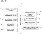
- Exposure apparatus 10 is equipped with: an illumination system 12; a reticle stage 14; a projection unit 16; a wafer stage device 20 including a wafer stage 22; a multipoint focal position measurement system 40; an alignment system 50; a control system thereof; and the like.
- wafer W is placed on wafer stage 22.
- illumination system 12 includes : a light source; and an illumination optical system that has an illuminance uniformizing optical system having an optical integrator, and a reticle blind (none of which is illustrated) .
- Illumination system 12 illuminates an illumination area IAR having a slit-like shape elongated in the X-axis direction on reticle R set (restricted) by the reticle blind (a masking system) with illumination light (exposure light) IL with almost uniform illuminance.
- illumination light IL for example, an ArF excimer laser beam (with a wavelength of 193nm) is used.
- Reticle stage 14 On reticle stage 14, reticle R having a pattern surface (a lower surface in FIG. 1 ) on which a circuit pattern and the like are formed is fixed by, for example, vacuum adsorption.
- Reticle stage 14 is finely drivable within an XY plane and also drivable at a predetermined scanning velocity in a scanning direction (the Y-axis direction that is a lateral direction on the page surface of FIG. 1 ), with a reticle stage drive system 32 (not illustrated in FIG. 1 , see FIG. 6 ) including, for example, a linear motor and the like.
- Positional information within the XY plane (including rotation information in the ⁇ z direction) of reticle stage 14 is constantly measured at a resolution of, for example, around 0.5 to 1 nm with a reticle stage position measurement system 34 including, for example, an interferometer system (or an encoder system).
- the measurement values of reticle stage position measurement system 34 are sent to a main controller 30 (not illustrated in FIG. 1 , see FIG. 6 ) .
- Main controller 30 controls the position (and the velocity) of reticle stage 14 by calculating the position of reticle stage 14 in the X-axis direction, the Y-axis direction and the ⁇ z direction on the basis of the measurement values of reticle stage position measurement system 34 and controlling reticle stage drive system 32 on the basis of this calculation result.
- exposure apparatus 10 is equipped with a reticle alignment system 18 (see FIG. 6 ) for performing position detection of reticle alignment marks formed on reticle R, though the reticle alignment system is not illustrated in FIG. 1 .
- reticle alignment system 18 an alignment system having a configuration as disclosed in, for example, U.S. Patent No. 5,646,413 , U.S. Patent Application Publication No. 2002/0041377 and the like can be used.
- Projection unit 16 is disposed below reticle stage 14 in FIG. 1 .
- Projection unit 16 includes a lens barrel 16a and projection optical system 16b stored within lens barrel 16a.
- projection optical system 16b for example, a dioptric system composed of a plurality of optical elements (lens elements) arrayed along optical axis AX parallel to the Z-axis direction is used.
- Projection optical system 16b is, for example, both-side telecentric, and has a predetermined projection magnification (such as 1/4 times, 1/5 times or 1/8 times).
- illumination area IAR on reticle R is illuminated with illumination system 12, by illumination light IL, which has passed through reticle R whose pattern surface is disposed almost coincident with a first plane (an object plane) of projection optical system 16b, a reduced image of a circuit pattern (a reduced image of a part of the circuit pattern) of reticle R within illumination area IAR is formed via projection optical system 16b (projection unit 16) onto an area (hereinafter, also referred to as an exposure area) IA, conjugate with illumination area IAR described above, on wafer W whose surface is coated with resist (sensitive agent) and which is disposed on a second plane (an image plane) side of projection optical system 16b.
- reticle R is moved in the scanning direction (the Y-axis direction) relative to illumination area IAR (illumination light IL) and also wafer W is moved in the scanning direction (the Y-axis direction) relative to exposure area IA (illumination light IL), and thereby the scanning exposure of one shot area (a divided area) on wafer W is performed and the pattern of reticle R is transferred onto the shot area. That is, in the present embodiment, a pattern is generated on wafer W by illumination system 12, reticle R and projection optical system 16b, and the pattern is formed on wafer W by exposure of a sensitive layer (a resist layer) on wafer W with illumination light IL.
- a sensitive layer a resist layer
- Wafer stage device 20 is equipped with wafer stage 22 disposed above a base board 28.
- Wafer stage 22 includes a stage main body 24, and a wafer table 26 mounted on stage main body 24.
- Stage main body 24 is supported on base board 28, via a clearance (an interspace, or a gap) of around several ⁇ m, by noncontact bearings (not illustrated), e.g., air bearings, fixed to the bottom surface of stage main body 24.
- Stage main body 24 is configured drivable relative to base board 28 in directions of three degrees of freedom (X, Y, ⁇ z) within a horizontal plane, by a wafer stage drive system 36 (not illustrated in FIG. 1 , see FIG. 6 ) including, for example, a linear motor (or a planar motor).
- Wafer stage drive system 36 includes a fine drive system that finely drives wafer table 26 relative to stage main body 24 in directions of six degrees of freedom (X, Y, Z, ⁇ x, ⁇ y and ⁇ z). Positional information of wafer table 26 in the directions of six degrees of freedom is constantly measured at a resolution of, for example, around 0.5 to 1 nm with a wafer stage position measurement system 38 including, for example, an interferometer system (or an encoder system). The measurement values of wafer stage position measurement system 38 are sent to main controller 30 (not illustrated in FIG. 1 , see FIG. 6 ).
- Main controller 30 controls the position (and the velocity) of wafer table 26 by calculating the position of wafer table 26 in the directions of six degrees of freedom on the basis of the measurement values of wafer stage position measurement system 38 and controlling wafer stage drive system 36 on the basis of this calculation result.
- Main controller 30 also controls the position of stage main body 24 within the XY plane on the basis of the measurement values of wafer stage position measurement system 38.
- Multipoint focal position measurement system 40 is a position measurement device of an oblique incidence method that measures positional information of wafer W in the Z-axis direction, which has a configuration similar to the one disclosed in, for example, U.S. Patent No. 5,448,332 and the like. As illustrated in FIG. 1 , multipoint focal position measurement system 40 is disposed on the further -Y side of alignment system 50 disposed on the -Y side of projection unit 16. Since the output of multipoint focal position measurement system 40 is used for autofocus control that will be described later, multipoint focal position measurement system 40 is referred to as an AF system 40 hereinafter.
- AF system 40 is equipped with: an irradiation system that irradiates the wafer W surface with a plurality of detection beams; and a beam receiving system that receives reflection beams, from the wafer W surface, of the plurality of detection beams (none of these systems is illustrated).
- a plurality of detection points of AF system 40 irradiation points of the detection beams are disposed at a predetermined interval along the X-axis direction on a surface to be detected, though the illustration of the detection points is omitted.
- the detection points are disposed in a matrix shape having one row and M columns (M is a total number of the detection points) or 2 rows and N columns (N is a half of the total number of the detection points) .
- the output of the beam receiving system is supplied to main controller 30 (see FIG. 6 ) .
- Main controller 30 obtains positional information in the Z-axis direction of the wafer W surface (surface position information) at the plurality of detection points on the basis of the output of the beam receiving system.
- the length in the X-axis direction of a detection area of the surface position information by AF system 40 (a disposed area of the plurality of detection points) is set equal to at least the length in the X-axis direction of one shot area set on wafer W.
- main controller 30 moves wafer W relative to the detection area of AF system 40 in the Y-axis direction and/or the X-axis direction as needed, and acquires the surface position information of wafer W on the basis of the output of AF system 40 at that time.
- Main controller 30 performs the acquisition of the surface position information as described above for all the shot areas set on wafer W, and associates the results of the acquisition with the positional information of wafer table 26 to store them as focus mapping information.
- alignment marks formed on wafer W and alignment system 50 of an off-axis type used in detection of the alignment marks will be described.
- At least one grating mark GM as illustrated in FIG. 2a is formed in each shot area on wafer W. Note that actually grating mark GM is formed in a scribe line of each shot area.
- Grating mark GM includes a first grating mark GMa and a second grating mark GMb.
- the first grating mark GMa is made up of a reflection-type diffraction grating in which grating lines extending in a direction (hereinafter, referred to as an ⁇ direction for the sake of convenience) that is at a 45 degree angle with respect to the X-axis within the XY plane are formed at a predetermined interval (e.g., a pitch P1 (P1 is an arbitrary numerical value)) in a direction (hereinafter, referred to as a ⁇ direction for the sake of convenience) orthogonal to the ⁇ direction within the XY plane, and which has a period direction in the ⁇ direction.
- a predetermined interval e.g., a pitch P1 (P1 is an arbitrary numerical value)
- the second grating mark GMb is made up of a reflection-type diffraction grating in which grating lines extending in the ⁇ direction are formed at a predetermined interval (e.g., a pitch P2 (P2 is an arbitrary numerical value)) in the ⁇ direction, and which has a period direction in the ⁇ direction.
- the first grating mark GMa and the second grating mark GMb are disposed consecutively (adjacently) in the X-axis direction so that the positions of the first grating mark GMa and the second grating mark GMb in the Y-axis direction are the same. Note that, in FIG.
- pitch P1 and pitch P2 may be the same numerical value or may be the numerical values different from each other.
- first grating mark GMa and the second grating mark GMb are in contact with each other in FIG. 2 , they need not be in contact with each other.
- alignment system 50 is equipped with: a light source 72 that emits a plurality of measurement beams L1 and L2; an objective optical system 60 that includes an objective transparent plate (which is also referred to as an objective optical element) 62 disposed facing wafer W; an irradiation system 70 that irradiates grating mark GM on wafer W with measurement beams L1 and L2 via objective transparent plate 62 while scanning the measurement beams L1 and L2 in the scanning direction (which is the Y-axis direction in the present embodiment and is also referred to as "a first direction” as needed); and a beam receiving system 80 that receives, via objective optical system 60, diffraction beams ⁇ L3 and ⁇ L4 from grating mark GM based measurement beams L1 and L2.
- a light source 72 that emits a plurality of measurement beams L1 and L2
- an objective optical system 60 that includes an objective transparent plate (which is also referred to as an objective optical element) 62 disposed facing wafer W
- Irradiation system 70 is equipped with: light source 72 described above; a movable mirror 74 disposed on optical paths of measurement beams L1 and L2; a half mirror (a beam splitter) 76 that reflects parts of measurement beams L1 and L2 reflected by movable mirror 74 toward wafer W and transmits the rest of the measurement beams; a beam position detection sensor 78 disposed on optical paths of measurement beams L1 and L2 transmitted (having passed) through half mirror 76; and the like.
- Light source 72 emits two measurement beams L1 and L2 having a broadband wavelength, to which the resist coated on wafer W (see FIG. 1 ) is insensitive, in the -Z direction. Note that, in FIG. 3 , the optical path of measurement beam L2 overlaps with the optical path of measurement beam L1, on the depth side of the paper surface.
- measurement beams L1 and L2 for example, white light is used.
- Movable mirror 74 for example, the well-known galvano mirror is used in the present embodiment.
- Movable mirror 74 has a reflection surface for reflecting measurement beams L1 and L2 that is configured capable of moving rotationally (rotating) around an axis line parallel to the X-axis.
- the angle of rotational movement of movable mirror 74 is controlled by main controller 30 (not illustrated in FIG. 3 , see Fig. 6 ) .
- the angle control of movable mirror 74 will be further described later.
- an optical member e. g., a prism or the like
- an optical member other than the galvano mirror may be used, as far as such an optical member can control the reflection angle of measurement beams L1 and L2.
- the position (the angle of a reflection surface) of half mirror 76 is fixed, which is different from movable mirror 74.
- the optical paths of the parts of measurements beams L1 and L2 reflected off the reflection surface of movable mirror 74 are bent to the -Z direction by half mirror 76, and then the parts of measurements beams L1 and L2 are incident almost perpendicularly on grating mark GM formed on wafer W, via objective transparent plate 62.
- movable mirror 74 is inclined at a 45 degree angle with respect to the Z-axis, and the parts of measurement beams L1 and L2 from movable mirror 74 are reflected off half mirror 76 in a direction parallel to the Z-axis.
- irradiation system 70 is configured so that measurement beams L1 and L2 emitted from objective transparent plate 62 are almost perpendicularly incident on grating mark GM formed on wafer W even in the case where movable mirror 74 is inclined at an angle other than a 45 degree angle with respect to the Z-axis.
- at least one optical member that is different from movable mirror 74 and half mirror 76 may be disposed on the optical paths of measurement beams L1 and L2 between light source 72 and objective transparent plate 62.
- Beam position detection sensor 78 has a photoelectric conversion element such as a PD (Photo Detector) array or a CCD (Charge Coupled Device), and its imaging plane is disposed on a plane conjugate with the wafer W surface.
- PD Photo Detector
- CCD Charge Coupled Device
- the distance between measurement beams L1 and L2 is set so that, of measurement beams L1 and L2 emitted from light source 72, measurement beam L1 is irradiated on the first grating mark GMa and measurement beam L2 is irradiated on the second grating mark GMb.
- alignment system 50 when the angle of the reflection surface of movable mirror 74 is changed, the respective incidence (irradiation) positions of measurement beams L1 and L2 on grating marks GMa and GMb (wafer W) are changed in the scanning direction (the Y-axis direction, the first direction) in accordance with the angle of the reflection surface of movable mirror 74 (see outlined arrows in FIG.
- main controller 30 can obtain irradiation position information of measurement beams L1 and L2 on wafer W on the basis of the output of beam position detection sensor 78.
- Objective optical system 60 is equipped with objective transparent plate 62, a detector-side transparent plate 64 and a grating plate 66.
- Objective transparent plate 62 is formed, into roughly a square shape in a planar view, of a transparent (light-transmissible) material, e.g., a quartz glass or the like, and objective transparent plate 62 includes a main section 62a disposed almost parallel to a horizontal plane and a plurality of transmission type diffraction gratings (hereinafter, simply referred to as "diffraction gratings”) formed on the lower surface of the main section 62a.
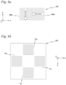
- FIG. 4a shows a plan view of objective transparent plate 62 when viewed from the lower surface side (the -Z side).
- diffraction gratings (diffraction gratings Ga 1 and Ga 2 ) with a period direction in the ⁇ direction and diffraction gratings (diffraction gratings Gb 1 and Gb 2 ) with a period direction in the ⁇ direction are formed.
- a grating pitch of each of diffraction gratings Ga 1 , Ga 2 , Gb 1 and Gb 2 is set to the same value in design as the grating pitches (P1 and P2 described above) of grating mark GMa and GMb (see FIG. 2a for each of them).
- Diffraction gratings Ga 1 and Ga 2 are disposed apart from each other in the ⁇ direction and diffraction gratings Gb 1 and Gb 2 are disposed apart from each other in the ⁇ direction. Further, diffraction gratings Ga 1 to Gb 2 are each formed so as to avoid the center portion of main section 62a. As illustrated in FIG. 3 , measurement beams L1 and L2 whose optical paths are bent to the -Z direction by half mirror 76 pass (are transmitted) through the center portion of main section 62a and are irradiated on grating mark GM.
- diffraction grating Ga 1 and/or diffraction grating Gb 1 are/is also referred to as (a) first optical component (S)
- diffraction grating Ga 2 and/or diffraction grating Gb 2 are/is also referred to as (a) second optical component (s).
- measurement beam L1 is irradiated on the first grating mark GMa via the transmissive area. Then, a plurality of +first-order diffraction beams (+L3), based on measurement beam L1, generated from the first grating mark GMa are incident on diffraction grating Ga 1 , and a plurality of -first-order diffraction beams (-L3), based on measurement beam L1, generated from the first grating mark GMa are incident on diffraction grating Ga 2 .
- a plurality of +first-order diffraction beams (+L4), based on measurement beam L2, generated from the second grating mark GMb are incident on diffraction grating Gb 1
- a plurality of -first-order diffraction beams (-L4), based on measurement beam L2, generated from the second grating mark GMb are incident on diffraction grating Gb 2 .
- the +first-order diffraction beams (+L3 and +L4) are diffracted by diffraction gratings Ga 1 and Gb 1 , respectively, and the -first-order diffraction beams (-L3 and -L4) are diffracted by diffraction gratings Ga 2 and Gb 2 , respectively.
- the respective zero-order diffraction beams from grating marks GMa and GMb of measurement beams L1 and L2 are to be attenuated because any diffraction gratings are not formed in the center portion of objective transparent plate 62 (i.e., the surface state of the transmissive area and the surface state of an area where diffraction gratings Ga 1 to Gb 2 are formed are optically different) .
- these zero-order diffraction beams may be attenuated at least in a range to prevent them from becoming measurement noise in beam receiving system 80.
- the respective predetermined-order diffraction beams described previously of the ⁇ first-order diffraction beams ( ⁇ L3 and ⁇ L4) emitted from objective transparent plate 62 (hereinafter, also referred to, collectively, as the diffraction beams from objective transparent plate 62) are incident on detector-side transparent plate 64 disposed above objective transparent plate 62, as illustrated in FIG. 3 .
- detector-side transparent plate 64 Since the configuration and the functions of detector-side transparent plate 64 are substantially the same as those of objective transparent plate 62, the description thereof will be omitted. That is, the diffraction beams from objective transparent plate 62 that are incident on detector-side transparent plate 64 are incident on transmission type diffraction gratings formed on the lower surface of a main section 64a of detector-side transparent plate 64, and thereby diffracted (their optical paths are bent), and are incident on grating plate 66 disposed above detector-side transparent plate 64.
- Grating plate 66 is made up of a plate-shaped member extending parallel to the Y-axis direction that is disposed parallel to detector-side transparent plate 64. As illustrated in Fig. 5a , readout diffraction gratings Ga and Gb are formed on grating plate 66.
- Readout diffraction grating Ga is a transmission type diffraction grating with a period direction in the ⁇ direction that corresponds to grating mark GMa (see FIG. 2a ) .
- Readout diffraction grating Gb is a transmission type diffraction grating with a period direction in the ⁇ direction that corresponds to grating mark GMb (see FIG. 2a ).
- main controller 30 controls movable mirror 74 of alignment system 50 while driving grating mark GM (i.e., wafer W) in the Y-axis direction (the first direction) relative to objective transparent plate 62 (i.e., alignment system 50) as shown by a double-headed arrow in FIG. 3 , and thereby causes measurement beams L1 and L2 to follow grating mark GM and scans measurement beams L1 and L2 in the Y-axis direction (the first direction).
- grating mark GM i.e., wafer W
- objective transparent plate 62 i.e., alignment system 50
- interference fringes are imaged (formed) on readout diffraction gratings Ga and Gb (see FIG. 5a ), by interference between the diffraction beams deriving from the diffraction beams ( ⁇ L3 and ⁇ L4) based on measurement beams L1 and L2.
- Beam receiving system 80 is equipped with: a detector 84; an optical system 86 that guides, to detector 84, light corresponding to images (interference fringes) formed on grating plate 66; and the like.
- optical system 86 has a spectral prism 86b, corresponding to white light being used as measurement beams L1 and L2.
- the light from grating plate 66 is spectrally split, for example, into respective colors of light, i.e., blue light, green light and red light, via spectral prism 86b.
- Detector 84 has photodetectors PD1 to PD3 that are independently provided corresponding to the respective colors described above. The output of each of photodetectors PD1 to PD3 that detector 84 has is supplied to main controller 30 (not illustrated in FIG. 3 , see FIG. 6 ).
- a signal (an interference signal) having a waveform as illustrated in FIG. 5b is obtained, as an example.
- Main controller 30 obtains the position of each of grating marks GMa and GMb, by calculation, from the phase of the signal described above. That is, in exposure apparatus 10 (see FIG. 1 ) of the present embodiment, alignment system 50 and main controller 30 (see FIG. 6 for each of them) configure an alignment device for obtaining positional information of grating mark GM formed on wafer W. Note that the signal as illustrated in FIG.
- grating marks GMa and GMb are generated on the basis of the relative position between grating marks GMa and GMb, and readout diffraction gratings Ga and Gb.
- the driving of grating marks GMa and GMb in the Y-axis direction and the scanning of measurement beams L1 and L2 in the Y-axis direction do not necessarily have to be completely in synchronization (their velocities do not strictly have to be coincident).
- reticle R and wafer W are loaded onto reticle stage 14 and wafer stage 22, respectively, and predetermined preparatory works such as reticle alignment using reticle alignment system 18 and wafer alignment (e.g., EGA (Enhanced Global Alignment) or the like) using alignment system 50 are performed.
- predetermined preparatory works such as reticle alignment using reticle alignment system 18 and wafer alignment (e.g., EGA (Enhanced Global Alignment) or the like) using alignment system 50 are performed.
- the preparatory works such as the reticle alignment referred to above and baseline measurement are disclosed in detail in, for example, U.S. Patent No.5,646,413 , U.S. Patent Application Publication No. 2002/0041377 and the like.
- the EGA following the reticle alignment and the baseline measurement is disclosed in detail in, for example, U.S. Patent No. 4,780,617 and the like.
- main controller 30 obtains surface position information of wafer W using AF system 40, prior to a position measurement operation of grating mark GM using alignment system 50. Then, main controller 30 controls the position and the attitude in the Z-axis direction (the tilt in the ⁇ x direction and the ⁇ z direction) of wafer table 26 on the basis of the surface position information described above and the offset value that has been obtained beforehand for each layer, and thereby causes objective optical system 60 of alignment system 50 to focus on grating mark GM.
- the offset value refers to the measurement value of AF system 40 that is obtained when the position and the attitude of wafer table 26 are adjusted so that the signal intensity (the contrast of the interference fringes) of alignment system 50 is maximized.
- the position and the attitude of wafer table 26 are controlled in almost real time, by using the surface position information of wafer W obtained immediately before the detection of grating mark GM by alignment system 50.
- the surface position detection of wafer W may be performed by receiving the light from grating mark GM subject to position measurement, concurrently with the position measurement of grating mark GM.
- wafer stage 22 is moved to an acceleration starting position for exposure with respect to the first shot area on wafer W, and reticle stage 14 is moved so that reticle R is positioned at an acceleration starting position. Then, reticle stage 14 and wafer stage 22 are driven in synchronization along the Y-axis direction, and thereby exposure with respect to the first shot area on wafer W is performed. Afterwards, exposure of wafer W is completed by performing exposure with respect to all the shot areas on wafer W.
- the travelling directions of the beams diffracted from grating mark GM (GMa and GMb) with a specific pitch (P1 and P2) are changed using objective transparent plate 62 on which diffraction gratings Ga 1 to Gb 2 are formed (utilizing the diffraction phenomenon of the beams), while a typical lens changes the travelling directions of beams utilizing the refraction phenomenon of the beams, and therefore, the increase in size of objective optical system 60 as a whole can be suppressed, compared with the case of using a lens as an objective optical element.
- alignment system 50 related to the present embodiment scans measurement beams L1 and L2 with respect to grating mark GM ((GMa and GMb), see FIG. 2a ) in the Y-axis direction while moving wafer W (wafer stage 22) in the Y-axis direction as illustrated in FIG.3 , and therefore, a position measurement operation of the grating mark GM can be performed concurrently with, for example, a movement operation of wafer stage 22 toward an exposure starting position that is performed after wafer W is loaded onto wafer stage 22.
- alignment system 50 related to the present embodiment scans the measurement beams so as to follow wafer W (grating mark GM) that is moved in the scanning direction, which allows for the measurement for a long period of time. Therefore, since the so-called moving average of the output can be taken, the influence of the vibration of the apparatus can be reduced. Further, if a mark in a line-and-space shape is detected using an image sensor (such as a CCD) as a beam receiving system of the alignment system, the other images than the images of lines completely parallel to the scanning direction cannot be detected (such images are distorted), when the measurement beams are scanned to follow wafer W that is moved in the scanning direction. In contrast, in the present embodiment, since the position measurement of grating mark GM is performed by causing the diffraction beams from the grating mark GM to interfere with each other, the mark detection can be reliably performed.
- an image sensor such as a CCD
- alignment system 50 related to the present embodiment has, for example, three photodetectors PD1 to PD3 (for blue light, green light and red light, respectively) as detector 84, corresponding to measurement beams L1 and L2 that are white light. Therefore, for example, by detecting overlay marks (not illustrated) formed on wafer W using the white light, and obtaining the color of the light with which the contrast of the interference fringes is the highest beforehand prior to wafer alignment, which output of the three photodetectors PD1 to PD3 exemplified above is optimal to be used in the wafer alignment can be determined.
- an exposure apparatus related to a second embodiment will be discussed. Since the exposure apparatus related to the present second embodiment is different only in the configuration of a part of an alignment system, from exposure apparatus 10 related to the first embodiment described previously, only the difference will be described below, and with regard to components that have the same configurations and functions as those in the first embodiment, the same reference signs as those in the first embodiment will be used and the description thereof will be omitted.
- FIG. 7a shows a plan view of an objective transparent plate (also referred to as an objective optical element) 162, when viewed from below (the -Z side), that an alignment system (the entire figure is not illustrated) related to the present second embodiment has.
- the alignment system related to the present second embodiment has an irradiation system and a beam receiving system that are similar to those of the first embodiment, though they are not illustrated.
- the diffraction beams ( ⁇ L3 and ⁇ L4) from grating marks GMa and GMb (see FIG. 2a for each of them) based on measurement beam L1 and measurement beam L2 are diffracted toward beam receiving system 80, by diffraction gratings Ga 1 to Gb 2 formed on main section 62a of objective transparent plate 62 (see FIG. 4b ), while in the present second embodiment, as illustrated in FIG.
- the diffraction beams ( ⁇ L3 and ⁇ L4) from grating marks GMa and GMb based on measurement beams L1 and L2 are deflected in parallel to the Z-axis toward beam receiving system 80, by a plurality of, e.g., four prisms groups Pa 1 , Pa 2 , Pb 1 and Pb 2 formed on the lower surface of a main section 162a of objective transparent plate 162, which is the difference between the first embodiment and the second embodiment. Accordingly, the configuration of Fig. 7b does not fall within the scope of claim 1. Note that white light is used as measurement beams L1 and L2 (see FIG.
- Prism group Pa 1 has a plurality of, e.g. , four prisms P 1 to P 4 .
- the four prisms P 1 to P 4 are right-angle prisms with a triangle-shaped X-Z cross section having the same length in the Y-axis direction, and are integrally fixed to the lower surface of main section 162a (or integrally formed with main section 162a) .
- the four prisms P 1 to P 4 are arrayed so that their centers are located at a predetermined interval on a diagonal line in the ⁇ direction. That is, the positions of the four prisms P 1 to P 4 in the Y-axis direction are different from each other.
- the positions on main section 162a and the refraction indices of prisms P 1 to P 4 are each set, so that each of a plurality of diffraction beams from grating mark GMa based on measurement beam L1 is deflected in parallel to the Z-axis (i.e., in accordance with the wavelength of each of the plurality of beams included in measurement beam L1).
- Prism group Pb 1 is disposed laterally symmetric with respect to prism group Pa 1 in FIG. 7a
- prism group Pa 2 is disposed vertically symmetric with respect to prism group Pb 1 in FIG. 7a
- prism group Pb 2 is disposed laterally symmetric with respect to prism group Pa 2 in FIG.
- the effect of suppressing the increase in size of the objective optical system of the alignment system can be obtained, in a similar manner to the first embodiment.
- grating marks GMa and GMb are irradiated with measurement beams L1 and L2 that correspond to grating marks GMa and GMb, respectively.
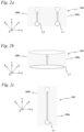
- the measurement beams are not limited thereto, and as illustrated in FIG. 2b , a single measurement beam L1 elongated (wide) in the X-axis direction may be irradiated on grating marks GMa and GMb.
- grating marks GMa and GMb are arrayed along the X-axis direction.
- the arrayed direction is not limited thereto, and as illustrated in FIG. 2c , grating marks GMa and GMb may be arrayed along the Y-axis direction.
- the position in the X-Y plane of grating mark GM can be obtained by scanning a single measurement beam L1 in the order of grating marks GMa and GMb (or the reversed order).
- the grating lines are at a 45 degree angle with respect to the X-axis and the Y-axis.
- the grating marks are not limited thereto, and for example, a grating mark GMy with a period direction in the Y-axis direction and a grating mark GMx with a period direction in the X-axis direction as illustrated in FIG. 8a may be used.
- an objective transparent plate (objective optical element) 262 equipped with diffraction gratings Gx 1 , Gx 2 , Gy 1 and Gy 2 corresponding to grating mark GMx and grating mark GMy as illustrated in FIG.
- objective transparent plate 62 as illustrated in FIG. 4a may be configured rotatable around the Z-axis by, for example, 45 degrees.
- diffraction gratings Ga 1 to Gb 2 that are formed on objective transparent plate 62 after such a rotation each have a period direction in the X-axis direction or the Y-axis direction, and therefore, objective transparent plate 62 functions in a similar manner to obj ective transparent plate 262 as illustrated in FIG. 8b . Consequently, detection of grating marks GM as illustrated in FIGS. 2a to 2c , respectively, and detection of grating mark GM as illustrated in FIG. 8a can be performed.
- objective optical system 60 equipped in the alignment system in the first embodiment and the second embodiment described above has detector-side transparent plate 64 that has substantially the same configuration as objective transparent plate 62 (or objective transparent plate 162 in the second embodiment).
- an optical system on the detector side is not limited thereto, but may be a lens similar to that of a conventional optical system.
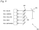
- beam receiving system 80 of alignment system 50 in the first embodiment described above spectrally splits white light with spectral prism 86b.
- the spectral means is not limited thereto, and like a beam receiving system 380 as illustrated in FIG. 9 , white light may be spectrally split toward photodetectors PD1 to PD5 disposed corresponding to the respective colors of light (e.g., blue light, green light, yellow light, red light and infrared light) by using a plurality of spectral filters 386.
- white light is used as measurement beams L1 and L2.
- the measurement beams are not limited to white light, and a plurality of beams with wavelengths different from each other may be used, in a similar manner to the second embodiment described above.
- a plurality of beams with wavelengths different from each other are used as measurement beams L1 and L2 in the second embodiment described above, white light may be used as measurement beams L1 and L2 in a similar manner to the first embodiment described above.
- alignment system 50 is used to detect the grating marks for performing the alignment (the fine alignment) between the reticle pattern and the wafer.
- the marks to be detected with the alignment system are not limited thereto, and , for example, the alignment system may be used to detect search marks formed on wafer W (grating marks with thicker linewidths and rougher pitches than grating marks GMa and GMb), immediately after wafer W is loaded onto wafer stage 22.
- an objective transparent plate which is also referred to as an objective optical element 362 as illustrated in FIG.
- diffraction gratings Ga 3 and Ga 4 with period directions in the ⁇ direction and diffraction gratings Gb 3 and Gb 4 with period directions in the ⁇ direction, according to the search marks, are additionally formed avoiding a transmissive area.
- the disposed position and the number of alignment system 50 can be changed as needed, and for example, a plurality of alignment systems 50 may be disposed at a predetermined interval in the X-axis direction. In this case, grating marks formed in a plurality of shot areas whose positions in the X-axis direction are different can be detected simultaneously. Further, in this case, a part of the plurality of alignment systems 50 may be configured movable with fine strokes in the X-axis direction. In this case, a plurality of grating marks formed on a wafer can be detected even if the shot map is different.
- the grating pitches of diffraction gratings Ga 1 to Gb 2 formed on objective transparent plate 62 equipped in alignment system 50 are set the same as the grating pitches of grating marks GMa and GMb subject to detection.
- the grating pitches of diffraction gratings Ga 1 to Gb 2 are not limited thereto, but for example, may be 1/n (n is a natural number) of the grating pitches of grating marks GMa and GMb.
- objective transparent plate 162 in the second embodiment described above has a plurality of prism groups Pa 1 to Pb 2 in order to bend the optical paths of diffractions beams ⁇ L3 and ⁇ L4 from grating mark GM.
- the optical components for bending the optical paths are not limited thereto, but may be, for example, mirrors or the like.
- illumination light IL is not limited to the ArF excimer laser beam (with a wavelength of 193 nm), but may be ultraviolet light such as a KrF excimer laser beam (with a wavelength of 248 nm), or vacuum ultraviolet light such as an F 2 laser beam (with a wavelength of 157 nm) .
- ultraviolet light such as a KrF excimer laser beam (with a wavelength of 248 nm)
- vacuum ultraviolet light such as an F 2 laser beam (with a wavelength of 157 nm) .
- a harmonic wave which is obtained by amplifying a single-wavelength laser beam in the infrared or visible range emitted by a DFB semiconductor laser or a fiber laser as vacuum ultraviolet light, with a fiber amplifier doped with, for example, erbium (or both erbium and ytterbium), and by converting the wavelength into ultraviolet light using a nonlinear optical crystal, may also be used.
- the wavelength of illumination light IL is not limited to the light having a wavelength equal to or more than 100 nm, and the light having a wavelength less than 100 nm may be used, and for example, the embodiments described above can also be applied to an EUV (Extreme Ultraviolet) exposure apparatus that uses an EUV light in a soft X-ray range (e.g., a wavelength range from 5 to 15 nm) . In addition, the embodiments described above can also be applied to an exposure apparatus that uses charged particle beams such as an electron beam or an ion beam.
- EUV Extreme Ultraviolet
- projection optical system in the exposure apparatus of each of the embodiments described above is not limited to a reduction system but may be either of an equal magnifying system or a magnifying system
- projection optical system 16b is not limited to a dioptric system but may be either of a catoptric system or a catadioptric system, and its projected image may be either of an inverted image or an erected image.
- a light-transmission type mask which is a light-transmissive substrate on which a predetermined light shielding pattern (or a phase pattern or a light attenuation pattern) is formed.
- a predetermined light shielding pattern or a phase pattern or a light attenuation pattern
- an electron mask which is also called a variable shaped mask, an active mask or an image generator, and includes, for example, a DMD (Digital Micro-mirror Device) that is a type of a non-emission type image display device (spatial light modulator) or the like) on which a light-transmitting pattern, a reflection pattern, or an emission pattern is formed on the basis of electronic data of the pattern that is to be exposed may also be used.
- a DMD Digital Micro-mirror Device
- a non-emission type image display device spatial light modulator
- each of the embodiments described above can also be applied to an exposure apparatus that performs an exposure operation in a state in which a space between a projection optical system and an object to be exposed (e.g., a wafer) is filled with a liquid (e.g., pure water), which is a so-called liquid immersion exposure apparatus, as is disclosed in, for example, U.S. Patent No. 8,004,650 .
- a liquid e.g., pure water
- each of the embodiments described above can also be applied to an exposure apparatus that is equipped with two wafer stages, as is disclosed in, for example, U.S. Patent Application Publication No. 2010/0066992 .
- each of the embodiments described above can also be applied to an exposure apparatus (lithography system) that forms line-and-space patterns on wafer W by forming interference fringes on wafer W, as is disclosed in, for example, U.S. Patent Application Publication No. 2001/0035168 . Further, each of the embodiments described above can also be applied to a reduction projection exposure apparatus by a step-and-stitch method that synthesizes a shot area and a shot area.
- each of the embodiments described above can also be applied to an exposure apparatus that synthesizes two reticle patterns on a wafer via a projection optical system and almost simultaneously performs double exposure of one shot area on the wafer by one-time scanning exposure, as is disclosed in, for example, U.S. Patent No. 6,611,316 .
- an object on which a pattern is to be formed is not limited to a wafer, but may be other objects such as a glass plate, a ceramic substrate, a film member, or a mask blank.
- the use of the exposure apparatus is not limited to the exposure apparatus used for manufacturing semiconductor devices, and can be widely applied also to, for example, an exposure apparatus for manufacturing liquid crystal display devices which transfers a liquid crystal display device pattern onto a square-shaped glass plate, and to an exposure apparatus for manufacturing organic EL, thin-film magnetic heads, imaging devices (such as CCDs), micromachines, DNA chips or the like.
- each of the embodiments described above can also be applied to an exposure apparatus that transfers a circuit pattern onto a glass substrate or a silicon wafer or the like, not only when producing microdevices such as semiconductor devices, but also when producing a reticle or a mask used in an exposure apparatus such as an optical exposure apparatus, an EUV exposure apparatus, an X-ray exposure apparatus, or an electron beam exposure apparatus.
- Electronic devices such as semiconductor devices are manufactured through the steps such as: a step in which the function/performance design of a device is performed; a step in which a reticle based on the design step is manufactured; a step in which a wafer is manufactured using a silicon material; a lithography step in which a pattern of a mask (the reticle) is transferred onto the wafer with the exposure apparatus (a pattern forming apparatus) of the embodiments described previously and the exposure method thereof; a development step in which the wafer that has been exposed is developed; an etching step in which an exposed member of the other section than a section where resist remains is removed by etching; a resist removal step in which the resist that is no longer necessary when etching is completed is removed; a device assembly step (including a dicing process, a bonding process, and a packaging process); and an inspection step.
- the exposure method described previously is implemented using the exposure apparatus of the embodiments described above and a device pattern is formed on the wafer
- the measurement device and the measurement method of the present invention are suitable for detecting grating marks. Further, the exposure apparatus and the exposure method of the present invention are suitable for exposing objects. Further, the device manufacturing method of the present invention is suitable for manufacturing microdevices.
Landscapes
- Physics & Mathematics (AREA)
- General Physics & Mathematics (AREA)
- Engineering & Computer Science (AREA)
- Multimedia (AREA)
- Exposure And Positioning Against Photoresist Photosensitive Materials (AREA)
- Length Measuring Devices By Optical Means (AREA)
- Exposure Of Semiconductors, Excluding Electron Or Ion Beam Exposure (AREA)
Claims (21)
- Messvorrichtung, aufweisend:ein Markierungserfassungssystem, das ein Bestrahlungssystem (70), ein optisches Objektivsystem (60) und ein Strahlempfangssystem (80) aufweist, wobei das Bestrahlungssystem (70) so konfiguriert ist, dass es eine Gittermarkierung (GM), die an einem Objekt vorgesehen ist, das in einer ersten Richtung bewegt wird, mit einem Messstrahl (L1, L2) bestrahlt, während es den Messstrahl in der ersten Richtung in Bezug auf die Gittermarkierung (GM) abtastet, wobei das optische Objektivsystem (60) ein optisches Objektivelement (62) enthält, das in der Lage ist, dem Objekt, das in der ersten Richtung bewegt wird, gegenüberzuliegen, und das Strahlempfangssystem (80) so konfiguriert ist, dass es einen Beugungsstrahl von der Gittermarkierung (GM) des Messstrahls (L1, L2) über das optische Objektivsystem (60) empfängt; undein Berechnungssystem, das so konfiguriert ist, dass es Positionsinformation der Gittermarkierung (GM) auf der Basis eines Erfassungsergebnisses des Markierungserfassungssystems erhält, wobeidas optische Objektivelement (62) so konfiguriert ist, dass es den an der Gittermarkierung erzeugten Beugungsstrahl in Richtung des Strahlempfangssystems beugt, wobei der durch das optische Objektivelement gebeugte Beugungsstrahl ein anderer Strahl als ein Strahl nullter Ordnung des Beugungsstrahls von der Gittermarkierung ist, undwobei das optische Objektivelement so konfiguriert ist, dass es einen Strahl nullter Ordnung des Beugungsstrahls von der Gittermarkierung abschwächt.
- Messvorrichtung nach Anspruch 1, wobei
das optische Objektivelement so konfiguriert ist, dass es den Beugungsstrahl parallel zu einer optischen Achse des optischen Objektivsystems in Richtung des Strahlempfangssystems beugt. - Messvorrichtung nach Anspruch 1 oder 2, wobei
das optische Objektivelement einen ersten Bereich aufweist, in dem ein optischer Pfad des Messstrahls von dem Bestrahlungssystem vorgesehen ist, und einen zweiten Bereich, in dem eine optische Komponente zum Beugen des Beugungsstrahls vorgesehen ist. - Messvorrichtung nach einem der Ansprüche 1 bis 3, wobei
das optische Objektivelement eine Vielzahl von Gitterlinien aufweist, die in einem vorbestimmten Abstand in einer Richtung gemäß einer Periodenrichtung der Gittermarkierung angeordnet sind. - Messvorrichtung nach Anspruch 4, wobei
der Abstand der Gitterlinie 1/n eines Gitterabstandes der Gittermarkierung ist, wobei n eine natürliche Zahl ist. - Messvorrichtung nach einem der Ansprüche 1 bis 5, wobei
das Markierungserfassungssystem ferner eine Rotationsvorrichtung aufweist, die so konfiguriert ist, dass sie das optische Objektivelement um eine optische Achse des optischen Objektivsystems rotiert. - Messvorrichtung nach Anspruch 6, wobei
die Messvorrichtung so konfiguriert ist, dass sie eine Position des optischen Objektivelements in einer Richtung um die optische Achse in Übereinstimmung mit einer Periodenrichtung eines Gitters der Gittermarkierung, die einer Messung unterzogen wird, steuert. - Messvorrichtung nach einem der Ansprüche 1 bis 7, wobeidie Gittermarkierung eine erste Gittermarkierung und eine zweite Gittermarkierung enthält, die jeweilige Periodenrichtungen in Richtungen aufweisen, die von der ersten Richtung und auch voneinander verschieden sind, unddas Bestrahlungssystem so konfiguriert ist, dass es die erste Gittermarkierung und die zweite Gittermarkierung mit dem Messstrahl bestrahlt, während es den Messstrahl in der ersten Richtung in Bezug auf die erste Gittermarkierung und die zweite Gittermarkierung abtastet, und das Strahlempfangssystem einen Beugungsstrahl von sowohl der ersten Gittermarkierung als auch der zweiten Gittermarkierung (GMb) empfängt, unddas Berechnungssystem so konfiguriert ist, dass es Positionsinformation von sowohl der ersten Gittermarkierung als auch der zweiten Gittermarkierung auf der Basis eines Erfassungsergebnisses des Markierungserfassungssystems erhält.
- Messvorrichtung nach einem der Ansprüche 1 bis 8, wobei das Strahlempfangssystem eine Vielzahl von Detektoren für verschiedene Farben des Strahls aufweist.
- Messvorrichtung nach Anspruch 10, wobei das Strahlempfangssystem so konfiguriert ist, dass es den Strahl auf die verschiedenen Farben aufteilt.
- Belichtungsvorrichtung (10), aufweisend:die Messvorrichtung nach einem der Ansprüche 1 bis 10;eine Positionssteuerungsvorrichtung, die so konfiguriert ist, dass sie eine Position des Objekts auf der Basis einer Ausgabe der Messvorrichtung steuert; undeine Musterbildungsvorrichtung, die so konfiguriert ist, dass sie ein vorbestimmtes Muster an dem Objekt durch Bestrahlung des Objekts mit einem Energiestrahl bildet.
- Verfahren zur Herstellung einer Vorrichtung, aufweisend:Belichten eines Substrats unter Verwendung der Belichtungsvorrichtung nach Anspruch 11; undEntwickeln des Substrats, das belichtet wurde.
- Messverfahren zum Messen von Positionsinformation einer Gittermarkierung (GM), die an einem Objekt vorgesehen ist, wobei das Verfahren aufweist:Bewegen des Objekts in einer ersten Richtung, unter einem optischen Objektivsystem (60) mit einem optischen Objektivelement (62), das in der Lage ist, dem Objekt gegenüberzuliegen;Bestrahlen der Gittermarkierung (GM) des Objekts, das bewegt wird, mit einem Messstrahl (L1, L2), während der Messstrahl in der ersten Richtung in Bezug auf die Gittermarkierung (GM) abgetastet wird;Empfangen eines Beugungsstrahls von der Gittermarkierung des Messstrahls mit einem Strahlempfangssystem (80) über das optische Objektivsystem; undErhalten von Positionsinformation der Gittermarkierung (GM) auf der Basis einer Ausgabe des Strahlempfangssystems, wobeiwobei das optische Objektivsystem den an der Gittermarkierung erzeugten Beugungsstrahl in Richtung des Strahlempfangssystems beugt, wobei der durch das optische Objektivelement gebeugte Beugungsstrahl ein anderer Strahl als ein Strahl nullter Ordnung des Beugungsstrahls von der Gittermarkierung ist, undwobei das optische Objektivelement einen Strahl nullter Ordnung des Beugungsstrahls von der Gittermarkierung abschwächt.
- Messverfahren nach Anspruch 13, wobei
das optische Objektivelement den Beugungsstrahl parallel zu einer optischen Achse des optischen Objektivsystems in Richtung des Strahlempfangssystems beugt. - Messverfahren nach Anspruch 13 oder 14, wobei
das optische Objektivelement den Beugungsstrahl beugt, wobei eine optische Komponente in einem zweiten Bereich vorgesehen ist, der sich von einem ersten Bereich unterscheidet, in dem ein optischer Pfad des Messstrahls vorgesehen ist. - Messverfahren nach einem der Ansprüche 13 bis 15, wobei
das optische Objektivelement eine Vielzahl von Gitterlinien aufweist, die in einem vorbestimmten Abstand in einer Richtung gemäß einer Periodenrichtung der Gittermarkierung angeordnet sind. - Messverfahren nach Anspruch 16, wobei
ein Abstand der Vielzahl von Gitterlinien 1/n eines Gitterabstandes der Gittermarkierung ist, wobei n eine natürliche Zahl ist. - Messverfahren nach einem der Ansprüche 13 bis 17, ferner aufweisend:
Rotieren des optischen Objektivelements um eine optische Achse des optischen Objektivsystems. - Messverfahren nach Anspruch 18, wobei
bei der Drehung eine Position des optischen Objektivelements in einer Richtung um die optische Achse in Übereinstimmung mit einer Periodenrichtung eines Gitters der Gittermarkierung, die einer Messung unterzogen wird, gesteuert wird. - Belichtungsverfahren, aufweisend:Messen von Positionsinformation einer an einem Objekt vorgesehenen Gittermarkierung unter Verwendung des Messverfahrens nach einem der Ansprüche 13 bis 19; undBelichten des Objekts mit einem Energiestrahl, während eine Position des Objekts auf der Basis der gemessenen Positionsinformation der Gittermarkierung, die gemessen wurde, gesteuert wird.
- Verfahren zur Herstellung einer Vorrichtung, aufweisend:Belichten eines Substrats unter Verwendung des Belichtungsverfahrens nach Anspruch 20; undEntwickeln des Substrats, das belichtet wurde.
Applications Claiming Priority (3)
| Application Number | Priority Date | Filing Date | Title |
|---|---|---|---|
| JP2014259759 | 2014-12-24 | ||
| PCT/JP2015/085848 WO2016104511A1 (ja) | 2014-12-24 | 2015-12-22 | 計測装置及び計測方法、露光装置及び露光方法、並びにデバイス製造方法 |
| EP15873079.6A EP3239776B1 (de) | 2014-12-24 | 2015-12-22 | Messvorrichtung und messverfahren, belichtungsvorrichtung und belichtungsverfahren sowie vorrichtungsherstellungsverfahren |
Related Parent Applications (1)
| Application Number | Title | Priority Date | Filing Date |
|---|---|---|---|
| EP15873079.6A Division EP3239776B1 (de) | 2014-12-24 | 2015-12-22 | Messvorrichtung und messverfahren, belichtungsvorrichtung und belichtungsverfahren sowie vorrichtungsherstellungsverfahren |
Publications (2)
| Publication Number | Publication Date |
|---|---|
| EP3926404A1 EP3926404A1 (de) | 2021-12-22 |
| EP3926404B1 true EP3926404B1 (de) | 2024-08-07 |
Family
ID=56150527
Family Applications (2)
| Application Number | Title | Priority Date | Filing Date |
|---|---|---|---|
| EP15873079.6A Active EP3239776B1 (de) | 2014-12-24 | 2015-12-22 | Messvorrichtung und messverfahren, belichtungsvorrichtung und belichtungsverfahren sowie vorrichtungsherstellungsverfahren |
| EP21177718.0A Active EP3926404B1 (de) | 2014-12-24 | 2015-12-22 | Messvorrichtung und messverfahren, expositionseinrichtung und expositionsverfahren und vorrichtungsherstellungsverfahren |
Family Applications Before (1)
| Application Number | Title | Priority Date | Filing Date |
|---|---|---|---|
| EP15873079.6A Active EP3239776B1 (de) | 2014-12-24 | 2015-12-22 | Messvorrichtung und messverfahren, belichtungsvorrichtung und belichtungsverfahren sowie vorrichtungsherstellungsverfahren |
Country Status (8)
| Country | Link |
|---|---|
| US (4) | US10372046B2 (de) |
| EP (2) | EP3239776B1 (de) |
| JP (1) | JP6459082B2 (de) |
| KR (2) | KR102022785B1 (de) |
| CN (2) | CN107407894B (de) |
| HK (1) | HK1246406A1 (de) |
| TW (2) | TWI690781B (de) |
| WO (1) | WO2016104511A1 (de) |
Families Citing this family (13)
| Publication number | Priority date | Publication date | Assignee | Title |
|---|---|---|---|---|
| EP3239776B1 (de) | 2014-12-24 | 2021-07-07 | Nikon Corporation | Messvorrichtung und messverfahren, belichtungsvorrichtung und belichtungsverfahren sowie vorrichtungsherstellungsverfahren |
| JP6917472B2 (ja) * | 2017-05-15 | 2021-08-11 | エーエスエムエル ネザーランズ ビー.ブイ. | メトロロジセンサ、リソグラフィ装置、及びデバイスを製造するための方法 |
| TWI796408B (zh) * | 2017-12-28 | 2023-03-21 | 美商魯道夫科技股份有限公司 | 順應機台以及形成其之基部的方法 |
| US11275146B2 (en) | 2018-11-08 | 2022-03-15 | Infineon Technologies Ag | LIDAR system with non-uniform sensitivity response |
| CN111752112B (zh) * | 2019-03-27 | 2021-09-10 | 上海微电子装备(集团)股份有限公司 | 掩膜对准标记组合、掩膜对准系统、光刻装置及其方法 |
| CN114391125B (zh) | 2019-09-09 | 2025-08-12 | Asml控股股份有限公司 | 具有远心转换器的放大率恒定的多级光学装置 |
| CN112838018B (zh) * | 2019-11-25 | 2023-09-15 | 致茂电子(苏州)有限公司 | 光学量测方法 |
| WO2021210052A1 (ja) * | 2020-04-13 | 2021-10-21 | 株式会社ニコン | 計測装置、露光装置、および計測方法 |
| US11988574B2 (en) * | 2020-11-24 | 2024-05-21 | Applied Materials, Inc. | Illumination system for AR metrology tool |
| KR102524462B1 (ko) * | 2022-03-28 | 2023-04-21 | (주)오로스 테크놀로지 | 오버레이 측정장치 |
| CN115881697B (zh) * | 2023-02-01 | 2023-06-02 | 广州粤芯半导体技术有限公司 | 对准标记组件和晶圆对准标记检测装置 |
| CN118518147B (zh) * | 2024-07-18 | 2024-09-24 | 泉州昆泰芯微电子科技有限公司 | 一种光检测装置及光学编码器 |
| CN120721357B (zh) * | 2025-08-20 | 2025-11-07 | 北京阿法龙科技有限公司 | 超表面光栅波导的衍射效率与视场角同步测试系统及方法 |
Family Cites Families (49)
| Publication number | Priority date | Publication date | Assignee | Title |
|---|---|---|---|---|
| US4780617A (en) | 1984-08-09 | 1988-10-25 | Nippon Kogaku K.K. | Method for successive alignment of chip patterns on a substrate |
| JPH0743245B2 (ja) | 1987-07-03 | 1995-05-15 | キヤノン株式会社 | アライメント装置 |
| US5489986A (en) * | 1989-02-28 | 1996-02-06 | Nikon Corporation | Position detecting apparatus |
| JPH03226608A (ja) * | 1990-01-31 | 1991-10-07 | Nec Corp | マスクとウエハの位置ずれ検出方法 |
| US5272501A (en) * | 1991-08-28 | 1993-12-21 | Nikon Corporation | Projection exposure apparatus |
| JPH05152188A (ja) * | 1991-11-26 | 1993-06-18 | Nikon Corp | 投影露光装置 |
| DE69223916T2 (de) * | 1991-10-03 | 1998-05-28 | Canon K.K., Tokio/Tokyo | Optische Kodiereinrichtung |
| JP3185373B2 (ja) * | 1991-10-03 | 2001-07-09 | キヤノン株式会社 | エンコーダ |
| EP0536655B1 (de) | 1991-10-03 | 1996-05-29 | Canon Kabushiki Kaisha | Messverfahren und Messgerät |
| KR100300618B1 (ko) | 1992-12-25 | 2001-11-22 | 오노 시게오 | 노광방법,노광장치,및그장치를사용하는디바이스제조방법 |
| US6153886A (en) * | 1993-02-19 | 2000-11-28 | Nikon Corporation | Alignment apparatus in projection exposure apparatus |
| JP3412704B2 (ja) | 1993-02-26 | 2003-06-03 | 株式会社ニコン | 投影露光方法及び装置、並びに露光装置 |
| JPH07142325A (ja) * | 1993-06-23 | 1995-06-02 | Nikon Corp | 位置合わせ装置 |
| JP3491346B2 (ja) * | 1994-08-22 | 2004-01-26 | 株式会社ニコン | 位置合わせ方法及びそれを用いた露光方法、並びに位置合わせ装置及びそれを用いた露光装置 |
| US5801389A (en) * | 1995-05-30 | 1998-09-01 | Nikon Corporation | Acousto-optic modulator, position detector using it, and projection exposure apparatus |
| JPH1022207A (ja) * | 1996-07-08 | 1998-01-23 | Nikon Corp | 位置検出装置 |
| JPH11265847A (ja) * | 1998-01-16 | 1999-09-28 | Canon Inc | 位置検出方法及び位置検出装置 |
| IL138374A (en) | 1998-03-11 | 2004-07-25 | Nikon Corp | An ultraviolet laser device and an exposure device that includes such a device |
| WO2001035168A1 (en) | 1999-11-10 | 2001-05-17 | Massachusetts Institute Of Technology | Interference lithography utilizing phase-locked scanning beams |
| KR20010085493A (ko) | 2000-02-25 | 2001-09-07 | 시마무라 기로 | 노광장치, 그 조정방법, 및 상기 노광장치를 이용한디바이스 제조방법 |
| JP2001250766A (ja) * | 2000-03-07 | 2001-09-14 | Nikon Corp | 位置計測装置並びに露光装置及び露光方法 |
| DE10011130A1 (de) | 2000-03-10 | 2001-09-13 | Mannesmann Vdo Ag | Entlüftungseinrichtung für einen Kraftstoffbehälter |
| US20020041377A1 (en) | 2000-04-25 | 2002-04-11 | Nikon Corporation | Aerial image measurement method and unit, optical properties measurement method and unit, adjustment method of projection optical system, exposure method and apparatus, making method of exposure apparatus, and device manufacturing method |
| JP2002083760A (ja) | 2000-09-08 | 2002-03-22 | Nikon Corp | X線投影露光装置およびx線投影露光方法および半導体デバイス |
| JP4714403B2 (ja) | 2001-02-27 | 2011-06-29 | エーエスエムエル ユーエス,インコーポレイテッド | デュアルレチクルイメージを露光する方法および装置 |
| TW529172B (en) | 2001-07-24 | 2003-04-21 | Asml Netherlands Bv | Imaging apparatus |
| JP3967935B2 (ja) * | 2002-02-25 | 2007-08-29 | 株式会社日立製作所 | 合わせ精度計測装置及びその方法 |
| JP2004022698A (ja) * | 2002-06-14 | 2004-01-22 | Nikon Corp | 位置検出用マークおよびこのマーク検出装置 |
| CN101872135B (zh) | 2002-12-10 | 2013-07-31 | 株式会社尼康 | 曝光设备和器件制造法 |
| US8411271B2 (en) | 2005-12-28 | 2013-04-02 | Nikon Corporation | Pattern forming method, pattern forming apparatus, and device manufacturing method |
| CN101385122B (zh) * | 2006-02-21 | 2010-12-08 | 株式会社尼康 | 图案形成装置、标记检测装置、曝光装置、图案形成方法、曝光方法及组件制造方法 |
| KR101333872B1 (ko) | 2006-02-21 | 2013-11-27 | 가부시키가이샤 니콘 | 패턴 형성 장치 및 패턴 형성 방법, 이동체 구동 시스템 및 이동체 구동 방법, 노광 장치 및 노광 방법, 그리고 디바이스 제조 방법 |
| EP2998983B1 (de) | 2006-12-27 | 2018-03-21 | Nikon Corporation | Trägerplattenvorrichtung, belichtungsvorrichtung und verfahren zur herstellung eines artikels |
| DE102008015631A1 (de) * | 2008-03-20 | 2009-09-24 | Carl Zeiss Sms Gmbh | Verfahren und Vorrichtung zur Vermessung von Masken für die Photolithographie |
| CN101251725B (zh) * | 2008-03-31 | 2010-09-15 | 上海微电子装备有限公司 | 用于光刻装置的对准系统和标记、对准方法以及光刻装置 |
| US8493547B2 (en) | 2009-08-25 | 2013-07-23 | Nikon Corporation | Exposure apparatus, exposure method, and device manufacturing method |
| KR101155888B1 (ko) * | 2010-07-23 | 2012-06-21 | 에스비리모티브 주식회사 | 이차 전지 |
| NL2008110A (en) * | 2011-02-18 | 2012-08-21 | Asml Netherlands Bv | Measuring method, measuring apparatus, lithographic apparatus and device manufacturing method. |
| US8539394B2 (en) | 2011-03-02 | 2013-09-17 | Carl Zeiss Sms Ltd. | Method and apparatus for minimizing overlay errors in lithography |
| JP6045588B2 (ja) * | 2011-08-23 | 2016-12-14 | エーエスエムエル ネザーランズ ビー.ブイ. | メトロロジ方法及び装置並びにデバイス製造方法 |
| KR101693950B1 (ko) * | 2011-09-29 | 2017-01-06 | 칼 짜이스 에스엠테 게엠베하 | 마이크로리소그래피 투영 노광 장치의 투영 대물 렌즈 |
| JP6025346B2 (ja) | 2012-03-05 | 2016-11-16 | キヤノン株式会社 | 検出装置、露光装置及びデバイスを製造する方法 |
| KR101761735B1 (ko) | 2012-03-27 | 2017-07-26 | 에이에스엠엘 네델란즈 비.브이. | 메트롤로지 방법 및 장치, 리소그래피 시스템 및 디바이스 제조 방법 |
| CN104321703B (zh) * | 2012-04-12 | 2017-09-22 | Asml控股股份有限公司 | 位置测量方法、位置测量设备、光刻设备以及装置制造方法、光学元件 |
| US9939742B2 (en) * | 2012-11-05 | 2018-04-10 | Asml Netherlands B.V. | Method and apparatus for measuring asymmetry of a microstructure, position measuring method, position measuring apparatus, lithographic apparatus and device manufacturing method |
| US9030661B1 (en) * | 2013-03-15 | 2015-05-12 | Kla-Tencor Corporation | Alignment measurement system |
| JP6344623B2 (ja) * | 2014-12-24 | 2018-06-20 | 株式会社ニコン | 移動体の制御方法、露光方法、デバイス製造方法、移動体装置、及び露光装置 |
| EP3239776B1 (de) * | 2014-12-24 | 2021-07-07 | Nikon Corporation | Messvorrichtung und messverfahren, belichtungsvorrichtung und belichtungsverfahren sowie vorrichtungsherstellungsverfahren |
| US10416577B2 (en) * | 2015-12-03 | 2019-09-17 | Asml Holding N.V. | Position measuring method of an alignment target |
-
2015
- 2015-12-22 EP EP15873079.6A patent/EP3239776B1/de active Active
- 2015-12-22 EP EP21177718.0A patent/EP3926404B1/de active Active
- 2015-12-22 CN CN201580076880.3A patent/CN107407894B/zh active Active
- 2015-12-22 JP JP2016566390A patent/JP6459082B2/ja active Active
- 2015-12-22 HK HK18105556.5A patent/HK1246406A1/zh unknown
- 2015-12-22 KR KR1020177020375A patent/KR102022785B1/ko active Active
- 2015-12-22 CN CN202010012207.6A patent/CN111045302B/zh active Active
- 2015-12-22 WO PCT/JP2015/085848 patent/WO2016104511A1/ja not_active Ceased
- 2015-12-22 KR KR1020197026384A patent/KR102284227B1/ko active Active
- 2015-12-24 TW TW104143485A patent/TWI690781B/zh active
- 2015-12-24 TW TW109107469A patent/TWI748363B/zh active
-
2017
- 2017-06-20 US US15/627,707 patent/US10372046B2/en active Active
-
2019
- 2019-05-31 US US16/428,223 patent/US10642169B2/en active Active
-
2020
- 2020-03-31 US US16/836,016 patent/US20200225592A1/en not_active Abandoned
-
2022
- 2022-06-10 US US17/837,107 patent/US12164236B2/en active Active
Also Published As
| Publication number | Publication date |
|---|---|
| EP3239776A4 (de) | 2018-09-19 |
| US10372046B2 (en) | 2019-08-06 |
| EP3239776B1 (de) | 2021-07-07 |
| TWI690781B (zh) | 2020-04-11 |
| CN111045302B (zh) | 2022-12-30 |
| KR20170097185A (ko) | 2017-08-25 |
| EP3926404A1 (de) | 2021-12-22 |
| TW201635054A (zh) | 2016-10-01 |
| KR102022785B1 (ko) | 2019-09-18 |
| TWI748363B (zh) | 2021-12-01 |
| EP3239776A1 (de) | 2017-11-01 |
| KR20190107187A (ko) | 2019-09-18 |
| CN111045302A (zh) | 2020-04-21 |
| US20180129144A1 (en) | 2018-05-10 |
| US12164236B2 (en) | 2024-12-10 |
| CN107407894A (zh) | 2017-11-28 |
| US10642169B2 (en) | 2020-05-05 |
| JP6459082B2 (ja) | 2019-01-30 |
| KR102284227B1 (ko) | 2021-07-30 |
| US20190285995A1 (en) | 2019-09-19 |
| US20200225592A1 (en) | 2020-07-16 |
| WO2016104511A1 (ja) | 2016-06-30 |
| CN107407894B (zh) | 2020-01-24 |
| JPWO2016104511A1 (ja) | 2017-09-28 |
| TW202028894A (zh) | 2020-08-01 |
| HK1246406A1 (zh) | 2018-09-07 |
| US20220317581A1 (en) | 2022-10-06 |
Similar Documents
| Publication | Publication Date | Title |
|---|---|---|
| US12164236B2 (en) | Measurement device and measurement method, exposure apparatus and exposure method, and device manufacturing method | |
| CN102017072B (zh) | 载置台装置、图案形成装置、曝光装置、载置台驱动方法、曝光方法、以及器件制造方法 | |
| US11994811B2 (en) | Control method of movable body, exposure method, device manufacturing method, movable body apparatus, and exposure apparatus | |
| CN101680783A (zh) | 移动体系统、图案形成装置、曝光装置及测量装置、以及器件制造方法 | |
| HK1245414A1 (en) | Measurement device and measurement method, exposure device and exposure method, and device production method | |
| JP2016143849A (ja) | 露光方法、デバイス製造方法、及び露光装置 | |
| JP2016149405A (ja) | 計測装置、露光装置、デバイス製造方法、及び計測方法 | |
| WO2016125790A1 (ja) | 計測装置及び計測方法、露光装置及び露光方法、並びにデバイス製造方法 | |
| HK1245500A1 (en) | Method for controlling moving body, exposure method, method for manufacturing device, moving body apparatus, and exposure apparatus |
Legal Events
| Date | Code | Title | Description |
|---|---|---|---|
| PUAI | Public reference made under article 153(3) epc to a published international application that has entered the european phase |
Free format text: ORIGINAL CODE: 0009012 |
|
| STAA | Information on the status of an ep patent application or granted ep patent |
Free format text: STATUS: THE APPLICATION HAS BEEN PUBLISHED |
|
| AC | Divisional application: reference to earlier application |
Ref document number: 3239776 Country of ref document: EP Kind code of ref document: P |
|
| AK | Designated contracting states |
Kind code of ref document: A1 Designated state(s): AL AT BE BG CH CY CZ DE DK EE ES FI FR GB GR HR HU IE IS IT LI LT LU LV MC MK MT NL NO PL PT RO RS SE SI SK SM TR |
|
| B565 | Issuance of search results under rule 164(2) epc |
Effective date: 20211119 |
|
| STAA | Information on the status of an ep patent application or granted ep patent |
Free format text: STATUS: REQUEST FOR EXAMINATION WAS MADE |
|
| 17P | Request for examination filed |
Effective date: 20220601 |
|
| RBV | Designated contracting states (corrected) |
Designated state(s): AL AT BE BG CH CY CZ DE DK EE ES FI FR GB GR HR HU IE IS IT LI LT LU LV MC MK MT NL NO PL PT RO RS SE SI SK SM TR |
|
| STAA | Information on the status of an ep patent application or granted ep patent |
Free format text: STATUS: EXAMINATION IS IN PROGRESS |
|
| 17Q | First examination report despatched |
Effective date: 20230306 |
|
| P01 | Opt-out of the competence of the unified patent court (upc) registered |
Effective date: 20230517 |
|
| GRAP | Despatch of communication of intention to grant a patent |
Free format text: ORIGINAL CODE: EPIDOSNIGR1 |
|
| STAA | Information on the status of an ep patent application or granted ep patent |
Free format text: STATUS: GRANT OF PATENT IS INTENDED |
|
| INTG | Intention to grant announced |
Effective date: 20240229 |
|
| GRAS | Grant fee paid |
Free format text: ORIGINAL CODE: EPIDOSNIGR3 |
|
| GRAA | (expected) grant |
Free format text: ORIGINAL CODE: 0009210 |
|
| STAA | Information on the status of an ep patent application or granted ep patent |
Free format text: STATUS: THE PATENT HAS BEEN GRANTED |
|
| AC | Divisional application: reference to earlier application |
Ref document number: 3239776 Country of ref document: EP Kind code of ref document: P |
|
| AK | Designated contracting states |
Kind code of ref document: B1 Designated state(s): AL AT BE BG CH CY CZ DE DK EE ES FI FR GB GR HR HU IE IS IT LI LT LU LV MC MK MT NL NO PL PT RO RS SE SI SK SM TR |
|
| REG | Reference to a national code |
Ref country code: GB Ref legal event code: FG4D |
|
| REG | Reference to a national code |
Ref country code: CH Ref legal event code: EP |
|
| REG | Reference to a national code |
Ref country code: IE Ref legal event code: FG4D |
|
| REG | Reference to a national code |
Ref country code: DE Ref legal event code: R096 Ref document number: 602015089506 Country of ref document: DE |
|
| REG | Reference to a national code |
Ref country code: NL Ref legal event code: FP |
|
| REG | Reference to a national code |
Ref country code: LT Ref legal event code: MG9D |
|
| PG25 | Lapsed in a contracting state [announced via postgrant information from national office to epo] |
Ref country code: NO Free format text: LAPSE BECAUSE OF FAILURE TO SUBMIT A TRANSLATION OF THE DESCRIPTION OR TO PAY THE FEE WITHIN THE PRESCRIBED TIME-LIMIT Effective date: 20241107 |
|
| REG | Reference to a national code |
Ref country code: AT Ref legal event code: MK05 Ref document number: 1711611 Country of ref document: AT Kind code of ref document: T Effective date: 20240807 |
|
| PG25 | Lapsed in a contracting state [announced via postgrant information from national office to epo] |
Ref country code: FI Free format text: LAPSE BECAUSE OF FAILURE TO SUBMIT A TRANSLATION OF THE DESCRIPTION OR TO PAY THE FEE WITHIN THE PRESCRIBED TIME-LIMIT Effective date: 20240807 Ref country code: PT Free format text: LAPSE BECAUSE OF FAILURE TO SUBMIT A TRANSLATION OF THE DESCRIPTION OR TO PAY THE FEE WITHIN THE PRESCRIBED TIME-LIMIT Effective date: 20241209 Ref country code: PL Free format text: LAPSE BECAUSE OF FAILURE TO SUBMIT A TRANSLATION OF THE DESCRIPTION OR TO PAY THE FEE WITHIN THE PRESCRIBED TIME-LIMIT Effective date: 20240807 Ref country code: GR Free format text: LAPSE BECAUSE OF FAILURE TO SUBMIT A TRANSLATION OF THE DESCRIPTION OR TO PAY THE FEE WITHIN THE PRESCRIBED TIME-LIMIT Effective date: 20241108 |
|
| PG25 | Lapsed in a contracting state [announced via postgrant information from national office to epo] |
Ref country code: BG Free format text: LAPSE BECAUSE OF FAILURE TO SUBMIT A TRANSLATION OF THE DESCRIPTION OR TO PAY THE FEE WITHIN THE PRESCRIBED TIME-LIMIT Effective date: 20240807 |
|
| PG25 | Lapsed in a contracting state [announced via postgrant information from national office to epo] |
Ref country code: LV Free format text: LAPSE BECAUSE OF FAILURE TO SUBMIT A TRANSLATION OF THE DESCRIPTION OR TO PAY THE FEE WITHIN THE PRESCRIBED TIME-LIMIT Effective date: 20240807 |
|
| PG25 | Lapsed in a contracting state [announced via postgrant information from national office to epo] |
Ref country code: AT Free format text: LAPSE BECAUSE OF FAILURE TO SUBMIT A TRANSLATION OF THE DESCRIPTION OR TO PAY THE FEE WITHIN THE PRESCRIBED TIME-LIMIT Effective date: 20240807 Ref country code: IS Free format text: LAPSE BECAUSE OF FAILURE TO SUBMIT A TRANSLATION OF THE DESCRIPTION OR TO PAY THE FEE WITHIN THE PRESCRIBED TIME-LIMIT Effective date: 20241207 |
|
| PG25 | Lapsed in a contracting state [announced via postgrant information from national office to epo] |
Ref country code: HR Free format text: LAPSE BECAUSE OF FAILURE TO SUBMIT A TRANSLATION OF THE DESCRIPTION OR TO PAY THE FEE WITHIN THE PRESCRIBED TIME-LIMIT Effective date: 20240807 |
|
| PG25 | Lapsed in a contracting state [announced via postgrant information from national office to epo] |
Ref country code: RS Free format text: LAPSE BECAUSE OF FAILURE TO SUBMIT A TRANSLATION OF THE DESCRIPTION OR TO PAY THE FEE WITHIN THE PRESCRIBED TIME-LIMIT Effective date: 20241107 Ref country code: ES Free format text: LAPSE BECAUSE OF FAILURE TO SUBMIT A TRANSLATION OF THE DESCRIPTION OR TO PAY THE FEE WITHIN THE PRESCRIBED TIME-LIMIT Effective date: 20240807 |
|
| PG25 | Lapsed in a contracting state [announced via postgrant information from national office to epo] |
Ref country code: RS Free format text: LAPSE BECAUSE OF FAILURE TO SUBMIT A TRANSLATION OF THE DESCRIPTION OR TO PAY THE FEE WITHIN THE PRESCRIBED TIME-LIMIT Effective date: 20241107 Ref country code: PT Free format text: LAPSE BECAUSE OF FAILURE TO SUBMIT A TRANSLATION OF THE DESCRIPTION OR TO PAY THE FEE WITHIN THE PRESCRIBED TIME-LIMIT Effective date: 20241209 Ref country code: PL Free format text: LAPSE BECAUSE OF FAILURE TO SUBMIT A TRANSLATION OF THE DESCRIPTION OR TO PAY THE FEE WITHIN THE PRESCRIBED TIME-LIMIT Effective date: 20240807 Ref country code: NO Free format text: LAPSE BECAUSE OF FAILURE TO SUBMIT A TRANSLATION OF THE DESCRIPTION OR TO PAY THE FEE WITHIN THE PRESCRIBED TIME-LIMIT Effective date: 20241107 Ref country code: LV Free format text: LAPSE BECAUSE OF FAILURE TO SUBMIT A TRANSLATION OF THE DESCRIPTION OR TO PAY THE FEE WITHIN THE PRESCRIBED TIME-LIMIT Effective date: 20240807 Ref country code: IS Free format text: LAPSE BECAUSE OF FAILURE TO SUBMIT A TRANSLATION OF THE DESCRIPTION OR TO PAY THE FEE WITHIN THE PRESCRIBED TIME-LIMIT Effective date: 20241207 Ref country code: HR Free format text: LAPSE BECAUSE OF FAILURE TO SUBMIT A TRANSLATION OF THE DESCRIPTION OR TO PAY THE FEE WITHIN THE PRESCRIBED TIME-LIMIT Effective date: 20240807 Ref country code: GR Free format text: LAPSE BECAUSE OF FAILURE TO SUBMIT A TRANSLATION OF THE DESCRIPTION OR TO PAY THE FEE WITHIN THE PRESCRIBED TIME-LIMIT Effective date: 20241108 Ref country code: FI Free format text: LAPSE BECAUSE OF FAILURE TO SUBMIT A TRANSLATION OF THE DESCRIPTION OR TO PAY THE FEE WITHIN THE PRESCRIBED TIME-LIMIT Effective date: 20240807 Ref country code: ES Free format text: LAPSE BECAUSE OF FAILURE TO SUBMIT A TRANSLATION OF THE DESCRIPTION OR TO PAY THE FEE WITHIN THE PRESCRIBED TIME-LIMIT Effective date: 20240807 Ref country code: BG Free format text: LAPSE BECAUSE OF FAILURE TO SUBMIT A TRANSLATION OF THE DESCRIPTION OR TO PAY THE FEE WITHIN THE PRESCRIBED TIME-LIMIT Effective date: 20240807 Ref country code: AT Free format text: LAPSE BECAUSE OF FAILURE TO SUBMIT A TRANSLATION OF THE DESCRIPTION OR TO PAY THE FEE WITHIN THE PRESCRIBED TIME-LIMIT Effective date: 20240807 |
|
| PG25 | Lapsed in a contracting state [announced via postgrant information from national office to epo] |
Ref country code: DK Free format text: LAPSE BECAUSE OF FAILURE TO SUBMIT A TRANSLATION OF THE DESCRIPTION OR TO PAY THE FEE WITHIN THE PRESCRIBED TIME-LIMIT Effective date: 20240807 Ref country code: SM Free format text: LAPSE BECAUSE OF FAILURE TO SUBMIT A TRANSLATION OF THE DESCRIPTION OR TO PAY THE FEE WITHIN THE PRESCRIBED TIME-LIMIT Effective date: 20240807 |
|
| PG25 | Lapsed in a contracting state [announced via postgrant information from national office to epo] |
Ref country code: EE Free format text: LAPSE BECAUSE OF FAILURE TO SUBMIT A TRANSLATION OF THE DESCRIPTION OR TO PAY THE FEE WITHIN THE PRESCRIBED TIME-LIMIT Effective date: 20240807 |
|
| PG25 | Lapsed in a contracting state [announced via postgrant information from national office to epo] |
Ref country code: CZ Free format text: LAPSE BECAUSE OF FAILURE TO SUBMIT A TRANSLATION OF THE DESCRIPTION OR TO PAY THE FEE WITHIN THE PRESCRIBED TIME-LIMIT Effective date: 20240807 |
|
| PG25 | Lapsed in a contracting state [announced via postgrant information from national office to epo] |
Ref country code: SK Free format text: LAPSE BECAUSE OF FAILURE TO SUBMIT A TRANSLATION OF THE DESCRIPTION OR TO PAY THE FEE WITHIN THE PRESCRIBED TIME-LIMIT Effective date: 20240807 |
|
| REG | Reference to a national code |
Ref country code: DE Ref legal event code: R097 Ref document number: 602015089506 Country of ref document: DE |
|
| PLBE | No opposition filed within time limit |
Free format text: ORIGINAL CODE: 0009261 |
|
| STAA | Information on the status of an ep patent application or granted ep patent |
Free format text: STATUS: NO OPPOSITION FILED WITHIN TIME LIMIT |
|
| REG | Reference to a national code |
Ref country code: DE Ref legal event code: R119 Ref document number: 602015089506 Country of ref document: DE |
|
| PG25 | Lapsed in a contracting state [announced via postgrant information from national office to epo] |
Ref country code: MC Free format text: LAPSE BECAUSE OF FAILURE TO SUBMIT A TRANSLATION OF THE DESCRIPTION OR TO PAY THE FEE WITHIN THE PRESCRIBED TIME-LIMIT Effective date: 20240807 |
|
| 26N | No opposition filed |
Effective date: 20250508 |
|
| REG | Reference to a national code |
Ref country code: CH Ref legal event code: PL |
|
| PG25 | Lapsed in a contracting state [announced via postgrant information from national office to epo] |
Ref country code: LU Free format text: LAPSE BECAUSE OF NON-PAYMENT OF DUE FEES Effective date: 20241222 |
|
| GBPC | Gb: european patent ceased through non-payment of renewal fee |
Effective date: 20241222 |
|
| PG25 | Lapsed in a contracting state [announced via postgrant information from national office to epo] |
Ref country code: SE Free format text: LAPSE BECAUSE OF FAILURE TO SUBMIT A TRANSLATION OF THE DESCRIPTION OR TO PAY THE FEE WITHIN THE PRESCRIBED TIME-LIMIT Effective date: 20240807 |
|
| REG | Reference to a national code |
Ref country code: BE Ref legal event code: MM Effective date: 20241231 |
|
| PG25 | Lapsed in a contracting state [announced via postgrant information from national office to epo] |
Ref country code: DE Free format text: LAPSE BECAUSE OF NON-PAYMENT OF DUE FEES Effective date: 20250701 |
|
| PG25 | Lapsed in a contracting state [announced via postgrant information from national office to epo] |
Ref country code: BE Free format text: LAPSE BECAUSE OF NON-PAYMENT OF DUE FEES Effective date: 20241231 Ref country code: GB Free format text: LAPSE BECAUSE OF NON-PAYMENT OF DUE FEES Effective date: 20241222 |
|
| PG25 | Lapsed in a contracting state [announced via postgrant information from national office to epo] |
Ref country code: FR Free format text: LAPSE BECAUSE OF NON-PAYMENT OF DUE FEES Effective date: 20241231 |
|
| PG25 | Lapsed in a contracting state [announced via postgrant information from national office to epo] |
Ref country code: CH Free format text: LAPSE BECAUSE OF NON-PAYMENT OF DUE FEES Effective date: 20241231 |
|
| PG25 | Lapsed in a contracting state [announced via postgrant information from national office to epo] |
Ref country code: IE Free format text: LAPSE BECAUSE OF NON-PAYMENT OF DUE FEES Effective date: 20241222 |
|
| PG25 | Lapsed in a contracting state [announced via postgrant information from national office to epo] |
Ref country code: RO Free format text: LAPSE BECAUSE OF FAILURE TO SUBMIT A TRANSLATION OF THE DESCRIPTION OR TO PAY THE FEE WITHIN THE PRESCRIBED TIME-LIMIT Effective date: 20240807 |
|
| PGFP | Annual fee paid to national office [announced via postgrant information from national office to epo] |
Ref country code: NL Payment date: 20251112 Year of fee payment: 11 |
|
| PG25 | Lapsed in a contracting state [announced via postgrant information from national office to epo] |
Ref country code: IT Free format text: LAPSE BECAUSE OF FAILURE TO SUBMIT A TRANSLATION OF THE DESCRIPTION OR TO PAY THE FEE WITHIN THE PRESCRIBED TIME-LIMIT Effective date: 20240807 |
|
| PG25 | Lapsed in a contracting state [announced via postgrant information from national office to epo] |
Ref country code: CY Free format text: LAPSE BECAUSE OF FAILURE TO SUBMIT A TRANSLATION OF THE DESCRIPTION OR TO PAY THE FEE WITHIN THE PRESCRIBED TIME-LIMIT Effective date: 20240807 |