EP3920210B1 - Dispositif d'optimisation/collimateur de flux pouvant être polarisé pour chambre de pulvérisation pvd - Google Patents
Dispositif d'optimisation/collimateur de flux pouvant être polarisé pour chambre de pulvérisation pvd Download PDFInfo
- Publication number
- EP3920210B1 EP3920210B1 EP21188409.3A EP21188409A EP3920210B1 EP 3920210 B1 EP3920210 B1 EP 3920210B1 EP 21188409 A EP21188409 A EP 21188409A EP 3920210 B1 EP3920210 B1 EP 3920210B1
- Authority
- EP
- European Patent Office
- Prior art keywords
- collimator
- apertures
- collimator assembly
- substantially vertical
- aspect ratio
- Prior art date
- Legal status (The legal status is an assumption and is not a legal conclusion. Google has not performed a legal analysis and makes no representation as to the accuracy of the status listed.)
- Active
Links
- 230000004907 flux Effects 0.000 title description 5
- 239000000758 substrate Substances 0.000 claims description 62
- 238000005477 sputtering target Methods 0.000 claims description 34
- NJPPVKZQTLUDBO-UHFFFAOYSA-N novaluron Chemical compound C1=C(Cl)C(OC(F)(F)C(OC(F)(F)F)F)=CC=C1NC(=O)NC(=O)C1=C(F)C=CC=C1F NJPPVKZQTLUDBO-UHFFFAOYSA-N 0.000 claims description 30
- 238000004544 sputter deposition Methods 0.000 claims description 29
- 230000002093 peripheral effect Effects 0.000 claims description 28
- 238000000034 method Methods 0.000 claims description 14
- 150000002500 ions Chemical class 0.000 claims description 11
- 230000008569 process Effects 0.000 claims description 9
- XAGFODPZIPBFFR-UHFFFAOYSA-N aluminium Chemical compound [Al] XAGFODPZIPBFFR-UHFFFAOYSA-N 0.000 claims description 7
- 229910052782 aluminium Inorganic materials 0.000 claims description 7
- 239000000463 material Substances 0.000 description 29
- 238000000151 deposition Methods 0.000 description 13
- 238000005240 physical vapour deposition Methods 0.000 description 13
- 230000008021 deposition Effects 0.000 description 9
- RYGMFSIKBFXOCR-UHFFFAOYSA-N Copper Chemical compound [Cu] RYGMFSIKBFXOCR-UHFFFAOYSA-N 0.000 description 5
- 239000010949 copper Substances 0.000 description 5
- 229910052802 copper Inorganic materials 0.000 description 5
- 239000010410 layer Substances 0.000 description 5
- 230000008901 benefit Effects 0.000 description 4
- 230000007423 decrease Effects 0.000 description 4
- 230000005684 electric field Effects 0.000 description 3
- 238000005516 engineering process Methods 0.000 description 3
- 239000010408 film Substances 0.000 description 3
- 238000001914 filtration Methods 0.000 description 3
- 239000010935 stainless steel Substances 0.000 description 3
- 229910001220 stainless steel Inorganic materials 0.000 description 3
- 238000004140 cleaning Methods 0.000 description 2
- 239000004020 conductor Substances 0.000 description 2
- 238000011109 contamination Methods 0.000 description 2
- 229940082150 encore Drugs 0.000 description 2
- 238000007667 floating Methods 0.000 description 2
- 230000010354 integration Effects 0.000 description 2
- 230000007935 neutral effect Effects 0.000 description 2
- 239000002245 particle Substances 0.000 description 2
- 239000004065 semiconductor Substances 0.000 description 2
- 229910052721 tungsten Inorganic materials 0.000 description 2
- 239000010937 tungsten Substances 0.000 description 2
- 208000000659 Autoimmune lymphoproliferative syndrome Diseases 0.000 description 1
- 229910000881 Cu alloy Inorganic materials 0.000 description 1
- RTAQQCXQSZGOHL-UHFFFAOYSA-N Titanium Chemical compound [Ti] RTAQQCXQSZGOHL-UHFFFAOYSA-N 0.000 description 1
- 230000001154 acute effect Effects 0.000 description 1
- 230000004888 barrier function Effects 0.000 description 1
- 239000011324 bead Substances 0.000 description 1
- 238000005513 bias potential Methods 0.000 description 1
- 238000000576 coating method Methods 0.000 description 1
- 239000002131 composite material Substances 0.000 description 1
- 238000010276 construction Methods 0.000 description 1
- 230000008878 coupling Effects 0.000 description 1
- 238000010168 coupling process Methods 0.000 description 1
- 238000005859 coupling reaction Methods 0.000 description 1
- 239000003989 dielectric material Substances 0.000 description 1
- 238000009792 diffusion process Methods 0.000 description 1
- 230000003292 diminished effect Effects 0.000 description 1
- 238000010494 dissociation reaction Methods 0.000 description 1
- 230000005593 dissociations Effects 0.000 description 1
- 238000009434 installation Methods 0.000 description 1
- 150000001455 metallic ions Chemical class 0.000 description 1
- TWNQGVIAIRXVLR-UHFFFAOYSA-N oxo(oxoalumanyloxy)alumane Chemical compound O=[Al]O[Al]=O TWNQGVIAIRXVLR-UHFFFAOYSA-N 0.000 description 1
- 230000000149 penetrating effect Effects 0.000 description 1
- 239000002344 surface layer Substances 0.000 description 1
- 229910052715 tantalum Inorganic materials 0.000 description 1
- GUVRBAGPIYLISA-UHFFFAOYSA-N tantalum atom Chemical compound [Ta] GUVRBAGPIYLISA-UHFFFAOYSA-N 0.000 description 1
- MZLGASXMSKOWSE-UHFFFAOYSA-N tantalum nitride Chemical compound [Ta]#N MZLGASXMSKOWSE-UHFFFAOYSA-N 0.000 description 1
- 239000013077 target material Substances 0.000 description 1
- 239000010409 thin film Substances 0.000 description 1
- 239000010936 titanium Substances 0.000 description 1
- 229910052719 titanium Inorganic materials 0.000 description 1
- WFKWXMTUELFFGS-UHFFFAOYSA-N tungsten Chemical compound [W] WFKWXMTUELFFGS-UHFFFAOYSA-N 0.000 description 1
- -1 tungsten nitride Chemical class 0.000 description 1
- 238000003466 welding Methods 0.000 description 1
Images


Classifications
-
- C—CHEMISTRY; METALLURGY
- C23—COATING METALLIC MATERIAL; COATING MATERIAL WITH METALLIC MATERIAL; CHEMICAL SURFACE TREATMENT; DIFFUSION TREATMENT OF METALLIC MATERIAL; COATING BY VACUUM EVAPORATION, BY SPUTTERING, BY ION IMPLANTATION OR BY CHEMICAL VAPOUR DEPOSITION, IN GENERAL; INHIBITING CORROSION OF METALLIC MATERIAL OR INCRUSTATION IN GENERAL
- C23C—COATING METALLIC MATERIAL; COATING MATERIAL WITH METALLIC MATERIAL; SURFACE TREATMENT OF METALLIC MATERIAL BY DIFFUSION INTO THE SURFACE, BY CHEMICAL CONVERSION OR SUBSTITUTION; COATING BY VACUUM EVAPORATION, BY SPUTTERING, BY ION IMPLANTATION OR BY CHEMICAL VAPOUR DEPOSITION, IN GENERAL
- C23C14/00—Coating by vacuum evaporation, by sputtering or by ion implantation of the coating forming material
- C23C14/22—Coating by vacuum evaporation, by sputtering or by ion implantation of the coating forming material characterised by the process of coating
- C23C14/34—Sputtering
- C23C14/3407—Cathode assembly for sputtering apparatus, e.g. Target
-
- H—ELECTRICITY
- H01—ELECTRIC ELEMENTS
- H01L—SEMICONDUCTOR DEVICES NOT COVERED BY CLASS H10
- H01L21/00—Processes or apparatus adapted for the manufacture or treatment of semiconductor or solid state devices or of parts thereof
- H01L21/02—Manufacture or treatment of semiconductor devices or of parts thereof
- H01L21/04—Manufacture or treatment of semiconductor devices or of parts thereof the devices having potential barriers, e.g. a PN junction, depletion layer or carrier concentration layer
- H01L21/18—Manufacture or treatment of semiconductor devices or of parts thereof the devices having potential barriers, e.g. a PN junction, depletion layer or carrier concentration layer the devices having semiconductor bodies comprising elements of Group IV of the Periodic Table or AIIIBV compounds with or without impurities, e.g. doping materials
- H01L21/28—Manufacture of electrodes on semiconductor bodies using processes or apparatus not provided for in groups H01L21/20 - H01L21/268
- H01L21/283—Deposition of conductive or insulating materials for electrodes conducting electric current
- H01L21/285—Deposition of conductive or insulating materials for electrodes conducting electric current from a gas or vapour, e.g. condensation
- H01L21/28506—Deposition of conductive or insulating materials for electrodes conducting electric current from a gas or vapour, e.g. condensation of conductive layers
- H01L21/28512—Deposition of conductive or insulating materials for electrodes conducting electric current from a gas or vapour, e.g. condensation of conductive layers on semiconductor bodies comprising elements of Group IV of the Periodic Table
- H01L21/2855—Deposition of conductive or insulating materials for electrodes conducting electric current from a gas or vapour, e.g. condensation of conductive layers on semiconductor bodies comprising elements of Group IV of the Periodic Table by physical means, e.g. sputtering, evaporation
-
- H—ELECTRICITY
- H01—ELECTRIC ELEMENTS
- H01J—ELECTRIC DISCHARGE TUBES OR DISCHARGE LAMPS
- H01J37/00—Discharge tubes with provision for introducing objects or material to be exposed to the discharge, e.g. for the purpose of examination or processing thereof
- H01J37/32—Gas-filled discharge tubes
- H01J37/34—Gas-filled discharge tubes operating with cathodic sputtering
- H01J37/3411—Constructional aspects of the reactor
- H01J37/3447—Collimators, shutters, apertures
-
- C—CHEMISTRY; METALLURGY
- C23—COATING METALLIC MATERIAL; COATING MATERIAL WITH METALLIC MATERIAL; CHEMICAL SURFACE TREATMENT; DIFFUSION TREATMENT OF METALLIC MATERIAL; COATING BY VACUUM EVAPORATION, BY SPUTTERING, BY ION IMPLANTATION OR BY CHEMICAL VAPOUR DEPOSITION, IN GENERAL; INHIBITING CORROSION OF METALLIC MATERIAL OR INCRUSTATION IN GENERAL
- C23C—COATING METALLIC MATERIAL; COATING MATERIAL WITH METALLIC MATERIAL; SURFACE TREATMENT OF METALLIC MATERIAL BY DIFFUSION INTO THE SURFACE, BY CHEMICAL CONVERSION OR SUBSTITUTION; COATING BY VACUUM EVAPORATION, BY SPUTTERING, BY ION IMPLANTATION OR BY CHEMICAL VAPOUR DEPOSITION, IN GENERAL
- C23C14/00—Coating by vacuum evaporation, by sputtering or by ion implantation of the coating forming material
- C23C14/04—Coating on selected surface areas, e.g. using masks
- C23C14/046—Coating cavities or hollow spaces, e.g. interior of tubes; Infiltration of porous substrates
-
- C—CHEMISTRY; METALLURGY
- C23—COATING METALLIC MATERIAL; COATING MATERIAL WITH METALLIC MATERIAL; CHEMICAL SURFACE TREATMENT; DIFFUSION TREATMENT OF METALLIC MATERIAL; COATING BY VACUUM EVAPORATION, BY SPUTTERING, BY ION IMPLANTATION OR BY CHEMICAL VAPOUR DEPOSITION, IN GENERAL; INHIBITING CORROSION OF METALLIC MATERIAL OR INCRUSTATION IN GENERAL
- C23C—COATING METALLIC MATERIAL; COATING MATERIAL WITH METALLIC MATERIAL; SURFACE TREATMENT OF METALLIC MATERIAL BY DIFFUSION INTO THE SURFACE, BY CHEMICAL CONVERSION OR SUBSTITUTION; COATING BY VACUUM EVAPORATION, BY SPUTTERING, BY ION IMPLANTATION OR BY CHEMICAL VAPOUR DEPOSITION, IN GENERAL
- C23C14/00—Coating by vacuum evaporation, by sputtering or by ion implantation of the coating forming material
- C23C14/06—Coating by vacuum evaporation, by sputtering or by ion implantation of the coating forming material characterised by the coating material
- C23C14/14—Metallic material, boron or silicon
- C23C14/16—Metallic material, boron or silicon on metallic substrates or on substrates of boron or silicon
-
- C—CHEMISTRY; METALLURGY
- C23—COATING METALLIC MATERIAL; COATING MATERIAL WITH METALLIC MATERIAL; CHEMICAL SURFACE TREATMENT; DIFFUSION TREATMENT OF METALLIC MATERIAL; COATING BY VACUUM EVAPORATION, BY SPUTTERING, BY ION IMPLANTATION OR BY CHEMICAL VAPOUR DEPOSITION, IN GENERAL; INHIBITING CORROSION OF METALLIC MATERIAL OR INCRUSTATION IN GENERAL
- C23C—COATING METALLIC MATERIAL; COATING MATERIAL WITH METALLIC MATERIAL; SURFACE TREATMENT OF METALLIC MATERIAL BY DIFFUSION INTO THE SURFACE, BY CHEMICAL CONVERSION OR SUBSTITUTION; COATING BY VACUUM EVAPORATION, BY SPUTTERING, BY ION IMPLANTATION OR BY CHEMICAL VAPOUR DEPOSITION, IN GENERAL
- C23C14/00—Coating by vacuum evaporation, by sputtering or by ion implantation of the coating forming material
- C23C14/22—Coating by vacuum evaporation, by sputtering or by ion implantation of the coating forming material characterised by the process of coating
- C23C14/34—Sputtering
- C23C14/35—Sputtering by application of a magnetic field, e.g. magnetron sputtering
-
- C—CHEMISTRY; METALLURGY
- C23—COATING METALLIC MATERIAL; COATING MATERIAL WITH METALLIC MATERIAL; CHEMICAL SURFACE TREATMENT; DIFFUSION TREATMENT OF METALLIC MATERIAL; COATING BY VACUUM EVAPORATION, BY SPUTTERING, BY ION IMPLANTATION OR BY CHEMICAL VAPOUR DEPOSITION, IN GENERAL; INHIBITING CORROSION OF METALLIC MATERIAL OR INCRUSTATION IN GENERAL
- C23C—COATING METALLIC MATERIAL; COATING MATERIAL WITH METALLIC MATERIAL; SURFACE TREATMENT OF METALLIC MATERIAL BY DIFFUSION INTO THE SURFACE, BY CHEMICAL CONVERSION OR SUBSTITUTION; COATING BY VACUUM EVAPORATION, BY SPUTTERING, BY ION IMPLANTATION OR BY CHEMICAL VAPOUR DEPOSITION, IN GENERAL
- C23C14/00—Coating by vacuum evaporation, by sputtering or by ion implantation of the coating forming material
- C23C14/22—Coating by vacuum evaporation, by sputtering or by ion implantation of the coating forming material characterised by the process of coating
- C23C14/54—Controlling or regulating the coating process
- C23C14/542—Controlling the film thickness or evaporation rate
-
- H—ELECTRICITY
- H01—ELECTRIC ELEMENTS
- H01J—ELECTRIC DISCHARGE TUBES OR DISCHARGE LAMPS
- H01J37/00—Discharge tubes with provision for introducing objects or material to be exposed to the discharge, e.g. for the purpose of examination or processing thereof
- H01J37/32—Gas-filled discharge tubes
- H01J37/32009—Arrangements for generation of plasma specially adapted for examination or treatment of objects, e.g. plasma sources
- H01J37/32403—Treating multiple sides of workpieces, e.g. 3D workpieces
-
- H—ELECTRICITY
- H01—ELECTRIC ELEMENTS
- H01J—ELECTRIC DISCHARGE TUBES OR DISCHARGE LAMPS
- H01J37/00—Discharge tubes with provision for introducing objects or material to be exposed to the discharge, e.g. for the purpose of examination or processing thereof
- H01J37/32—Gas-filled discharge tubes
- H01J37/32431—Constructional details of the reactor
- H01J37/32458—Vessel
- H01J37/32477—Vessel characterised by the means for protecting vessels or internal parts, e.g. coatings
-
- H—ELECTRICITY
- H01—ELECTRIC ELEMENTS
- H01J—ELECTRIC DISCHARGE TUBES OR DISCHARGE LAMPS
- H01J37/00—Discharge tubes with provision for introducing objects or material to be exposed to the discharge, e.g. for the purpose of examination or processing thereof
- H01J37/32—Gas-filled discharge tubes
- H01J37/34—Gas-filled discharge tubes operating with cathodic sputtering
- H01J37/3464—Operating strategies
- H01J37/347—Thickness uniformity of coated layers or desired profile of target erosion
-
- H—ELECTRICITY
- H01—ELECTRIC ELEMENTS
- H01L—SEMICONDUCTOR DEVICES NOT COVERED BY CLASS H10
- H01L21/00—Processes or apparatus adapted for the manufacture or treatment of semiconductor or solid state devices or of parts thereof
- H01L21/70—Manufacture or treatment of devices consisting of a plurality of solid state components formed in or on a common substrate or of parts thereof; Manufacture of integrated circuit devices or of parts thereof
- H01L21/71—Manufacture of specific parts of devices defined in group H01L21/70
- H01L21/768—Applying interconnections to be used for carrying current between separate components within a device comprising conductors and dielectrics
- H01L21/76838—Applying interconnections to be used for carrying current between separate components within a device comprising conductors and dielectrics characterised by the formation and the after-treatment of the conductors
Definitions
- Implementations of the present disclosure generally relate to an apparatus and method for uniform sputter deposition of materials into the bottom and sidewalls of high aspect ratio features on a substrate.
- Sputtering also known as physical vapor deposition (PVD) is widely used to deposit metallic features in integrated circuits. Sputtering is used to deposit layers for use as diffusion barriers, seed layers, primary conductors, antireflection coatings, and etch stops.
- a source material such as a target, is bombarded by ions strongly accelerated by an electric field. The bombardment ejects material from the target and the material then deposits on the substrate.
- ejected particles may travel in varying directions, rather than generally orthogonal to the substrate surface, resulting in overhanging structures formed on corners of high aspect ratio features in the substrate. Overhang may undesirably result in holes or voids formed within the deposited material, resulting in diminished electrical conductivity of the formed feature. Higher aspect ratio geometries have a higher degree of difficulty to fill without voids.
- collimator sputtering One technique developed to allow the use of sputtering to deposit thin films in the bottom of a high aspect ratio feature is collimator sputtering.
- a collimator is a filtering plate positioned between a sputtering source and a substrate.
- the collimator typically has a uniform thickness and includes a number of passages formed through the thickness. Sputtered material passes through the collimator on its path from the sputtering source to the substrate.
- the collimator filters out or collects material that would otherwise strike the workpiece at acute angles exceeding a desired angle.
- Document US 2009/3608739 A1 relates to an apparatus and method for uniform sputter depositing of materials into the bottom and sidewalls of high aspect ratio features on a substrate.
- a collimator for mechanical and electrical coupling with a shield member can be positioned between a sputtering target and a substrate support pedestal is provided.
- Document WO 93/13542 A1 relates to a collimator for sputter coating wherein the unit cells of the collimator taper longitudinally in the direction of the wafer.
- the collimator may be of one-piece construction and the unit cells may have an overall frusto-conical volume.
- Document WO 2016/085805 A1 forms part of the state of the art according to Article 54(3) EPC, and discloses a collimator for use in a substrate processing chamber.
- the collimator has a housing that includes a central region, a peripheral region, and a transitional region placed between the central and peripheral regions.
- Apertures are provided in the central region having a first aspect ratio.
- Second apertures are provided in the peripheral region having a second aspect ratio less than the first aspect ratio.
- Third multiple apertures are provided in the transitional region, such that the third apertures are cut so that the transitional region forms a conical shape surrounding the central region.
- the actual amount of material filtering accomplished by a given collimator depends on the aspect ratio of the apertures through the collimator. Material such as particles traveling on a path approaching normal to the substrate pass through the collimator and are deposited on the substrate. This allows improved coverage in the bottom of high aspect ratio features.
- certain problems exist with the use of prior art collimators which typically have an overall hexagonal shape. Unfortunately, PVD chambers with prior art collimators often suffer from cell clogging and leave a six-point deposition near an edge of the substrate due to shadowing of the corners of the hexagonal collimator.
- Implementations of the present disclosure generally relate to an apparatus and method for uniform sputter deposition of materials into the bottom and sidewalls of high aspect ratio features on a substrate.
- the invention is set forth in the claims.
- a collimator assembly having a collimator is provided according to claim 1.
- the collimator comprises a honeycomb structure having walls defining and separating apertures, wherein the apertures include a first plurality of apertures in a central region having a first aspect ratio; a second plurality of apertures in a peripheral region having a second aspect ratio less than the first aspect ratio; and a third plurality of apertures in a transitional region disposed between the central region and the peripheral region.
- the walls that define the third plurality of apertures of the transitional region form a conical shape surrounding the central region, and a shield portion coupled with the collimator is provided.
- the shield portion includes a top ring; a support ledge below the top ring, the support ledge extending radially outward; and a cylindrical band extending downward from the support ledge, wherein the cylindrical band includes a first substantially vertical portion; and a radially inward sloped portion extending downward from the first substantially vertical portion, wherein the radially inward sloped portion extends across a portion of the second plurality of apertures in the peripheral region.
- a substrate-processing chamber comprises a chamber body defining an inner volume, a sputtering target disposed in an upper portion of the inner volume, a substrate support disposed below the sputtering target, and a collimator assembly according to embodiments of the invention and for encircling the sputtering target.
- a collimator that is biasable is provided.
- the ability to bias the collimator allows control of the electric field through which the sputter species pass.
- a collimator that has a high effective aspect ratio while maintaining a low aspect ratio along the periphery of the collimator of the hexagonal array of the collimator is provided.
- a collimator with a steep entry edge in the hexagonal array is provided.
- FIG. 1 depicts an exemplary implementation of a substrate-processing chamber 100 having one implementation of a process kit 140 capable of processing a substrate 154.
- the processing chamber is coupled with a controller 101.
- the process kit 140 includes a one-piece lower shield 180 and a collimator assembly 108.
- the collimator assembly 108 includes a one-piece upper shield portion 186 coupled with a collimator portion 110.
- the processing chamber 100 comprises a sputtering chamber, also called a physical vapor deposition (PVD) chamber, capable of depositing, for example, titanium, aluminum oxide, aluminum, copper, tantalum, tantalum nitride, tungsten, or tungsten nitride, on a substrate.
- PVD physical vapor deposition
- PVD chambers examples include the ALPS ® Plus and SIP EnCoRe ® PVD processing chambers, both commercially available from Applied Materials, Inc., Santa Clara, of California. It is contemplated that processing chambers available from other manufactures may benefit from the implementations described herein.
- the processing chamber 100 has a chamber body 105 that defines an inner process volume 106.
- the chamber body 105 includes a chamber wall 150, a grounded conductive adapter 144, and a conductive flange 184 disposed above the chamber wall 150.
- the chamber wall 150 may be grounded.
- the conductive flange 184 is positioned between a first dielectric isolator ring 143 and a second dielectric isolator ring 147.
- One or more RF power sources 151 provide a bias potential through a matching network 155 to the conductive flange 184 to energize the one-piece upper shield portion 186 and the collimator portion 110.
- the processing chamber 100 includes a sputtering source, such as a sputtering target 142 having a sputtering surface 145, and a substrate support pedestal 152, for receiving a substrate 154 (e.g., a semiconductor substrate) thereon, the support pedestal 152 having a peripheral edge 153.
- the substrate support pedestal 152 may be located within the chamber wall 150.
- the processing chamber 100 includes the sputtering target 142 supported by the grounded conductive adapter 144 through a dielectric isolator 146.
- the sputtering target 142 comprises the material to be deposited on the surface of the substrate 154 during sputtering, and may include copper for depositing as a seed layer in high aspect ratio features formed in the substrate 154.
- the sputtering target 142 may also include a bonded composite of a metallic surface layer of sputterable material, such as copper, and a backing layer of a structural material, such as aluminum.
- the substrate support pedestal 152 supports a substrate 154 having high aspect ratio features to be sputter coated, the bottoms of which are in planar opposition to a principal surface of the sputtering target 142.
- the substrate support pedestal 152 has a planar substrate-receiving surface disposed generally parallel to the sputtering surface 145 of the sputtering target 142.
- the substrate support pedestal 152 may be vertically movable through a bellows 158 connected to a bottom chamber wall 160 to allow the substrate 154 to be transferred onto the substrate support pedestal 152 through a load lock valve (not shown) in a lower portion of the processing chamber 100. The substrate support pedestal 152 may then be raised to a deposition position as shown.
- processing gas may be supplied from a gas source 162 through a mass flow controller 164 into the lower portion of the processing chamber 100.
- a controllable direct current (DC) power source 148 coupled to the processing chamber 100, may be used to apply a negative voltage or bias to the sputtering target 142.
- a radio frequency (RF) power source 156 may be coupled to the substrate support pedestal 152 to induce a DC self-bias on the substrate 154.
- the substrate support pedestal 152 is grounded.
- the substrate support pedestal 152 is electrically floated.
- a magnetron 170 is positioned above the sputtering target 142.
- the magnetron 170 may include a plurality of magnets 172 supported by a base plate 174 connected to a shaft 176, which may be axially aligned with the central axis of the processing chamber 100 and the substrate 154.
- the magnets 172 are aligned in a kidney-shaped pattern. The magnets 172 produce a magnetic field within the processing chamber 100 near the front face of the sputtering target 142 to generate plasma, such that a significant flux of ions strike the sputtering target 142, causing sputter emission of target material.
- the magnets 172 may be rotated about the shaft 176 to increase uniformity of the magnetic field across the surface of the sputtering target 142.
- the magnetron 170 is a small magnet magnetron.
- the magnets 172 may be both rotated and moved reciprocally in a linear direction parallel or substantially parallel to the face of the sputtering target 142 to produce a spiral motion.
- the magnets 172 may be rotated about both a central axis and an independently-controlled secondary axis to control both their radial and angular positions.
- a first set of magnets 194 may be disposed adjacent the chamber wall 150 to assist generating an electronic field to the metallic ions dislodged from the sputtering target 142.
- a second set of magnets 195 may be disposed adjacent to the sputtering target 142 to assist in generating an electrode field to dislodge materials from the sputtering target 142. It is noted that the numbers of the magnets disposed around the processing chamber 100 may be as many as needed to improve plasma dissociation and sputtering efficiency.
- the processing chamber 100 includes the one-piece lower shield 180, which may be grounded, having a support flange 182 supported by and electrically coupled to the chamber wall 150.
- the one-piece upper shield portion 186 is supported by and electrically coupled to the conductive flange 184 of the grounded conductive adapter 144.
- the one-piece upper shield portion 186 and the one-piece lower shield 180 are electrically coupled, as are the grounded conductive adapter 144 and the chamber wall 150.
- both the one-piece upper shield portion 186 and the one-piece lower shield 180 are comprised of stainless steel.
- both the one-piece upper shield portion 186 and the one-piece lower shield 180 are comprised of aluminum.
- the processing chamber 100 includes a middle shield (not shown) coupled to the one-piece upper shield portion 186.
- the one-piece upper shield portion 186 and the one-piece lower shield 180 are electrically floating within the processing chamber 100.
- the one-piece upper shield portion 186 and the one-piece lower shield 180 may be coupled to an electrical power source.
- the one-piece upper shield portion 186 has an upper portion that closely fits an annular side recess of the sputtering target 142 with a narrow gap 188 between the one-piece upper shield portion 186 and the sputtering target 142, which is sufficiently narrow to prevent plasma from penetrating and sputter coating the dielectric isolator 146.
- the one-piece lower shield 180 extends downwardly into a cylindrical outer band 196, which generally extends along the chamber wall 150 to below the top surface of the substrate support pedestal 152.
- the one-piece lower shield 180 may have a base plate 198 extending radially inward from the cylindrical outer band 196.
- the base plate 198 may include an upwardly extending cylindrical inner band 103 surrounding the perimeter of the substrate support pedestal 152.
- a cover ring 102 rests on the top of the cylindrical inner band 103 when the substrate support pedestal 152 is in a lower, loading position and rests on the outer periphery of the substrate support pedestal 152 when the substrate support pedestal 152 is in an upper, deposition position to protect the substrate support pedestal 152 from sputter deposition.
- the one-piece lower shield 180 encircles the sputtering surface 145 of the sputtering target 142 that faces the substrate support pedestal 152 and encircles a peripheral wall of the substrate support pedestal 152.
- the one-piece lower shield 180 covers and shadows the chamber wall 150 of the processing chamber 100 to reduce deposition of sputtering deposits originating from the sputtering surface 145 of the sputtering target 142 onto the components and surfaces behind the one-piece lower shield 180.
- the one-piece lower shield 180 can protect the surfaces of the substrate support pedestal 152, portions of the substrate 154, the chamber wall 150, and the bottom chamber wall 160 of the processing chamber 100.
- directional sputtering may be achieved by positioning the collimator assembly 108 between the sputtering target 142 and the substrate support pedestal 152.
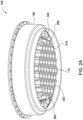
- FIG. 2A depicts a perspective view of a collimator assembly 108 in accordance with implementations of the present disclosure.
- FIG. 2B depicts another perspective view of the collimator assembly 108 in accordance with implementations of the present disclosure.
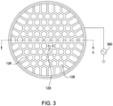
- FIG. 3 depicts a top view of the collimator assembly 108 of FIGS. 2A-2B that may be disposed in the processing chamber 100 of FIG. 1 .
- the collimator assembly 108 includes a one-piece upper shield portion 186 coupled with a collimator portion 110.
- the collimator portion 110 includes a plurality of apertures to direct gas and/or material flux within the processing chamber 100.
- the collimator portion 110 may be mechanically and electrically coupled to the one-piece upper shield portion 186. In one implementation, the collimator portion 110 may be coupled to a middle shield (not shown), positioned lower in the processing chamber 100. In one implementation, the collimator portion 110 is integral to the one-piece upper shield portion 186, as shown in FIGS. 2A-2B . In one implementation, the collimator portion 110 is welded to the one-piece upper shield portion 186. In one implementation, the collimator portion 110 and the one-piece upper shield portion 186 are machined from a single mass of material. In one implementation, the collimator portion 110 and the one-piece upper shield portion 186 are comprised of a material selected from aluminum, copper, and stainless steel.
- the one-piece upper shield portion 186 and the collimator portion 110 are formed as separate pieces and coupled together using suitable attachment means, such as welding.
- the collimator portion 110 may be electrically floating within the processing chamber 100.
- the collimator portion 110 may be coupled to an electrical power source.
- the collimator portion 110 is generally a body or a honeycomb structure 218 having walls 126 defining and separating hexagonal aperture(s) 128 in a close-packed arrangement.
- An aspect ratio of the hexagonal apertures 128 may be defined as the depth of the hexagonal aperture 128 (equal to the thickness of the collimator) divided by the width 129 of the hexagonal aperture 128.
- the thickness of the walls 126 is between about 0.06 inches (1.524 millimeters) and about 0.18 inches (4.572 millimeters).
- the thickness of the walls 126 is between about 0.12 inches (3.048 millimeters) and about 0.15 inches (3.81 millimeters).
- the collimator portion 110 is comprised of a material selected from aluminum, copper, and stainless steel.
- the honeycomb structure 218 of the collimator portion 110 may serve as an integrated flux optimizer to improve the flow path, ion fraction, and ion trajectory behavior of ions passing through the collimator portion 110.
- the walls 126 adjacent to a shield portion have an entrance angle portion 406 and a radius.
- the one-piece upper shield portion 186 of the collimator portion 110 may assist in the installation of the collimator portion 110 into the processing chamber 100.
- the collimator portion 110 may be machined from a single mass of aluminum.
- the collimator portion 110 may optionally be coated or anodized.
- the collimator portion 110 may be made from other materials compatible with the processing environment, and may be comprised of one or more sections.
- the walls 126 of the collimator portion 110 may be textured (e.g., bead blasted) to improve adhesion of high stress films (e.g., copper alloys) to the walls 126.
- the collimator portion 110 may be electrically biased in bipolar mode to control the direction of the ions passing through the collimator portion 110.
- a controllable direct current (DC) or AC collimator power source 390 may be coupled to the collimator portion 110 to provide an alternating pulsed positive or negative voltage to the collimator portion 110 to bias the collimator portion 110.
- the power source 390 is a DC power source.
- the collimator portion 110 functions as a filter to trap ions and neutral species that are emitted from the material from the sputtering target 142 at angles exceeding a selected angle, near normal relative to the substrate 154.
- the hexagonal apertures 128 of the collimator portion 110 are designed to allow a different percentage of ions emitted from a center or a peripheral region of the material from the sputtering target 142 to pass through the collimator portion 110.
- both the number of ions and the angle of arrival of ions deposited onto peripheral regions and center regions of the substrate 154 are adjusted and controlled. Therefore, material may be more uniformly sputter deposited across the surface of the substrate 154. Additionally material may be more uniformly deposited on the bottom and sidewalls of high aspect ratio features, particularly high aspect ratio vias and trenches located near the periphery of the substrate 154.
- FIG. 4 depicts a cross-sectional view of the collimator assembly 108 of FIGS. 2A-2B in accordance with implementations of the present disclosure.
- the collimator portion 110 includes the body or honeycomb structure 218 having a central region 220 having a first plurality of apertures 320 with a high aspect ratio, such as from about 2.5:1 to about 3:1.
- the aspect ratio of the central region 220 is from about 2.6:1 to about 2.7:1.
- the aspect ratio of a second plurality of apertures 340 of the collimator portion 110 in an outer peripheral region 240 decreases relative to the first plurality of apertures 320 in the central region 220.
- the second plurality of apertures 340 in the outer peripheral region 240 have an aspect ratio of from about 1:1 to about 2:1. In one implementation, the second plurality of apertures 340 in the outer peripheral region 240 has an aspect ratio of about 1:1. A higher aspect ratio allows for more apertures in the central region 220 of the collimator portion 110. In one implementation, the central region includes 61 apertures.
- the radial decrease of the hexagonal apertures 128 is accomplished by providing a third plurality of apertures 360 in a transitional region 260 disposed between the central region 220 and the outer peripheral region 240.
- the walls 126 defining the third plurality of apertures 360 are cut along a predetermined angle " ⁇ " so that the transitional region 260 forms a conical shape surrounding the first plurality of apertures 320.
- the predetermined angle is between 15 degrees and 45 degrees.
- the transitional region advantageously provides a circular profile 280 of apertures in the central region 220 that overcomes the six-point deposition near an edge of the substrate 154 due to shadowing caused by corners of a conventional hexagonal collimator.
- Upper portions of the walls 126 defining the hexagonal apertures 128 have an entrance angle portion 406 to decrease a rate at which the hexagonal apertures 128 are clogged by sputtered material.
- the entrance angle portion 406 extends a predetermined distance 402 into the hexagonal aperture 128 and is formed at a predetermined angle 404.
- the predetermined distance 402 is between about 0.15 inches (3.81 millimeters) to about 1 inch (2.54 centimeters) and the predetermined angle is between about 2 degrees and about 16 degrees.
- the predetermined distance 402 and the predetermined angle 404 are about 0.15 inches (3.81 millimeters) and 15 degrees, respectively.
- the predetermined distance 402 and the predetermined angle 404 are about 1 inch (2.54 centimeters) and 2.5 degrees respectively.
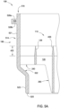
- FIG. 5A depicts a cross-sectional view of a portion of the collimator assembly 108 of FIGS. 2A-2B .
- the one-piece upper shield portion 186 has a diameter sized to encircle the sputtering surface 145 of the sputtering target 142 that faces the substrate support pedestal 152, the peripheral edge 153 of the substrate support pedestal 152, and shadows the grounded conductive adapter 144 and the chamber wall 150 of the processing chamber 100.
- the one-piece upper shield portion 186 serves to reduce deposition of sputtering deposits originating from the sputtering surface 145 of the sputtering target 142 onto the surfaces of the substrate support pedestal 152, overhanging edge of the substrate 154, the grounded conductive adapter 144, the chamber wall 150, and the bottom chamber wall 160 of the processing chamber 100.
- the one-piece upper shield portion 186 comprises a top ring 516. There is a support ledge 526 immediately below the top ring 516. The support ledge 526 extends radially outward towards the conductive flange 184 of the processing chamber 100.
- the support ledge 526 comprises a top surface 528a and a bottom surface 528b.
- the bottom surface 528b of the support ledge 526 may comprise a plurality of protrusions (not shown) to align the one-piece upper shield portion 186 with the conductive flange 184 supporting the one-piece upper shield portion 186.
- the support ledge 526 of the one-piece upper shield portion 186 has a plurality of counterbores (not shown) shaped and sized to receive a fastener to affix the one-piece upper shield portion 186 to the conductive flange 184.
- the support ledge 526 of the one-piece upper shield portion 186 may be secured to the conductive flange 184 by a plurality of fasteners (e.g., screws).
- the plurality of fasteners is from 30 to 40 (e.g., 36). Increasing the number of fasteners securing the one-piece upper shield portion 186 to the conductive flange 184 provides improved temperature control of the one-piece upper shield portion 186.
- a cylindrical band 514 Extending downward from the top ring 516 of the one-piece upper shield portion 186 is a cylindrical band 514 having a first vertical or substantially vertical portion 521, a radially inwardly sloped portion 522 and a second vertical or substantially vertical portion 523.
- the first vertical or substantially vertical portion 521 extends downward from the top ring 516 to the radially inwardly sloped portion 522.
- the radially inwardly sloped portion 522 has an angle " ⁇ " from about 40 to about 50 degrees (e.g., from about 45 to about 50 degrees) relative to the first substantially vertical portion 521 of the cylindrical band 514. As depicted in FIG.
- the radially inwardly sloped portion 522 extends across a portion of the second plurality of apertures 340 in the outer peripheral region 240.
- the second vertical or substantially vertical portion 523 extends downward from the radially inwardly sloped portion 522 and terminated in a rounded edge 525.
- the radially inwardly sloped portion 522 of the cylindrical band 514 to, for example, provide a surface for sputtered deposits that have flaked off from the top ring 516 and for sputtered deposits from the periphery of the sputtering target 142, to attach thereto. This effectively minimizes the contamination of substrate 154, especially around the edge.
- the collimator portion 110 is coupled with the first vertical or substantially vertical portion 521 of the cylindrical band 514. In one implementation, the collimator portion 110 and the first vertical or substantially vertical portion 521 are machined from a single mass of material.
- the cylindrical band 514 extends downward from the support ledge 526 to an elevation below the honeycomb structure 218.
- the cylindrical band 514 extends to an elevation below the outer peripheral region 240 of the collimator portion 110.
- the first vertical or substantially vertical portion 521 extends to an elevation below the second plurality of apertures 340 of the outer peripheral region 240 of the collimator portion 110.
- the second vertical or substantially vertical portion 523 extends to an elevation below the first plurality of apertures 320 of the central region 220 of the collimator portion 110.
- FIG. 5B depicts a cross-sectional view of a portion of another implementation of a collimator assembly 548 of FIGS. 2A-2B .
- the collimator assembly 548 of FIG. 5B is similar to the collimator assembly 108 except that the cylindrical band 514 of FIG. 5B is shorter than the cylindrical band 514 of FIG. 5A .
- the cylindrical band 514 of collimator assembly 548 has the first vertical or substantially vertical portion 521, the radially inwardly sloped portion 522 and a second vertical or substantially vertical portion 553.
- the second vertical or substantially vertical portion 553 of collimator assembly 548 is shorter than the second vertical or substantially vertical portion 523 of collimator assembly 108.
- the second vertical or substantially vertical portion 553 of collimator assembly 548 is shorter than the central region 220 of the honeycomb structure 218.
- the second vertical or substantially vertical portion 553 extends to an elevation below the second plurality of apertures 340 of the outer peripheral region 240 but does not extend to an elevation below the first plurality of apertures 320 of the central region 220.
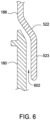
- FIG. 6 depicts a partial cross-sectional view of the intersection of the one-piece upper shield portion 186 and the one-piece lower shield 180.
- the second vertical or substantially vertical portion 523 may be positioned to cover the interface between the one-piece lower shield 180 and the one-piece upper shield portion 186, creating a labyrinth gap 602 between the one-piece lower shield 180 and the one-piece upper shield portion 186.
- the labyrinth gap 602 prevents conductive material from creating a surface bridge between the one-piece lower shield 180 and the one-piece upper shield portion 186, thus maintaining electrical discontinuity.
- collimator and/or a collimator assembly are disclosed in the present disclosure.
- a collimator includes a honeycomb structure having walls defining and separating hexagonal apertures.
- the hexagonal apertures include a first plurality of hexagonal apertures in a central region having a first aspect ratio; a second plurality of hexagonal apertures in a peripheral region having a second aspect ratio less than the first aspect ratio; and a third plurality of hexagonal apertures in a transitional region disposed between the central region and the peripheral region, wherein walls defining the third plurality of apertures of the transitional region form a conical shape surrounding the central region, and an upper portion of the walls include an entrance angle portion.
- the entrance angle portion can have a predetermined angle from about 2 degrees to about 16 degrees, particularly the entrance angle portion has a predetermined angle of about 2.5 degrees and has a length of about 2.54 centimeters or the entrance angle portion has a predetermined angle of about 15 degrees and has a length of about 3.81 millimeters.
- the first aspect ratio can be from about 2.5:1 to about 3:1 and the second aspect ratio is from about 1:1 to about 2:1.
- the collimator assembly includes a collimator portion.
- the collimator portion includes a honeycomb structure having walls defining and separating hexagonal apertures.
- the hexagonal apertures include a first plurality of hexagonal apertures in a central region having a first aspect ratio; a second plurality of hexagonal apertures in a peripheral region having a second aspect ratio less than the first aspect ratio; and a third plurality of hexagonal apertures in a transitional region disposed between the central region and the peripheral region, wherein walls defining the third plurality of apertures of the transitional region form a conical shape surrounding the central region, and an upper portion of the walls include an entrance angle portion; and a shield portion coupled with the collimator.
- the shield portion includes a top ring; a support ledge below the top ring, the support ledge extending radially outward; and a cylindrical band extending downward from the support ledge to an elevation below the honeycomb structure.
- the cylindrical band may include a first substantially vertical portion; and a radially inward sloped portion extending downward from the first substantially vertical portion, particularly further including a second substantially vertical portion extending downward from the radially inward sloped portion.
- the radially inward sloped portion may extend across a portion of the second plurality of apertures in the peripheral region.
- the first plurality of apertures, the second plurality of apertures, and the third plurality of apertures may be textured.
- the entrance angle portion can have a predetermined angle of from about 2 degrees to about 16 degrees, particularly wherein the entrance angle portion has a predetermined angle of about 2.5 degrees and has a length of about 2.54 centimeters.
- the first aspect ratio of the first plurality of apertures can be from about 2.5:1 to about 3:1, and particularly the second aspect ratio can be from about 1:1 to about 2:1.
- the radially inwardly sloped portion can have an angle from about 40 to about 50 degrees relative to the first substantially vertical portion.
- a collimator assembly that is biasable is provided.
- the ability to bias the collimator assembly allows control of the electric field through which the sputter species pass.
- a collimator assembly that has a high effective aspect ratio while maintaining a low aspect ratio along the periphery of the collimator assembly of the hexagonal array of the collimator assembly is provided.
- a collimator assembly with a steep entry edge in the hexagonal array is provided. It has been found that use of a steep entry edge in the collimator assembly substantially reduces deposition overhang and clogging of the cells of the hexagonal array in comparison with prior art collimator designs.
- a collimator assembly that has a cylindrical band with a radially inwardly sloped portion is provided.
- the radially inwardly sloped portion provide a surface for sputtered deposits that have flaked off from the other portions of the collimator assembly and for sputtered deposits from the periphery of the sputtering target to attach thereto.
- the readily inwardly slope portion effectively minimizes the contamination of substrates, especially around the edge.
- these various features substantially increase film uniformity and extend the life of the collimator assembly and process kit while reducing periods between cleaning.
Landscapes
- Chemical & Material Sciences (AREA)
- Engineering & Computer Science (AREA)
- Physics & Mathematics (AREA)
- Analytical Chemistry (AREA)
- Plasma & Fusion (AREA)
- Mechanical Engineering (AREA)
- Organic Chemistry (AREA)
- Metallurgy (AREA)
- Materials Engineering (AREA)
- Chemical Kinetics & Catalysis (AREA)
- Manufacturing & Machinery (AREA)
- General Physics & Mathematics (AREA)
- Condensed Matter Physics & Semiconductors (AREA)
- Computer Hardware Design (AREA)
- Microelectronics & Electronic Packaging (AREA)
- Power Engineering (AREA)
- Physical Vapour Deposition (AREA)
- Electrodes Of Semiconductors (AREA)
- Physical Deposition Of Substances That Are Components Of Semiconductor Devices (AREA)
Claims (14)
- Ensemble collimateur (108), comprenant :un collimateur (110), comprenantune structure en nid d'abeilles (218) ayant des parois (126) définissant et séparant des ouvertures (128), dans laquelle les ouvertures incluent :une première pluralité d'ouvertures (320) dans une région centrale (220) ayant un premier rapport d'aspect ;une deuxième pluralité d'ouvertures (340) dans une région périphérique (240) ayant un deuxième rapport d'aspect, inférieur au premier rapport d'aspect ; etune troisième pluralité d'ouvertures (360) dans une région de transition (260) disposée entre la région centrale (220) et la région périphérique (240),dans laquelle les parois définissant la troisième pluralité d'ouvertures (360) de la région de transition (260) forment une forme conique entourant la région centrale (220) ; etune partie de protection (186) couplée au collimateur (110), la partie de protection comprenant :un anneau supérieur (516) ;un rebord de support (526) en dessous de l'anneau supérieur (516), le rebord de support (526) s'étendant radialement vers l'extérieur ; etune bande cylindrique (514) s'étendant vers le bas à partir du rebord de support (526), dans lequel la bande cylindrique (514) comprend :une première partie sensiblement verticale (521) ; etune partie inclinée radialement vers l'intérieur (522) s'étendant vers le bas à partir de la première partie sensiblement verticale (521), dans laquelle la partie inclinée radialement vers l'intérieur (522) s'étend à travers une partie de la deuxième pluralité d'ouvertures (340) dans la région périphérique (240).
- Ensemble collimateur (108) de la revendication 1, comprenant en outre :
une deuxième partie sensiblement verticale (523) s'étendant vers le bas à partir de la partie inclinée radialement vers l'intérieur (522). - Ensemble collimateur (108) de la revendication 2, dans lequel la deuxième partie sensiblement verticale (523) s'étend jusqu'à une élévation en dessous de la deuxième pluralité d'ouvertures (340) mais ne s'étend pas jusqu'à une élévation en dessous de la première pluralité d'ouvertures (320).
- Ensemble collimateur (108) de la revendication 2, dans lequel la deuxième partie sensiblement verticale (523) s'étend jusqu'à une élévation en dessous de la première puralité d'ouvertures (320).
- Ensemble collimateur (108) de la revendication 1, dans lequel les parois définissant la première pluralité d'ouvertures (320), la deuxième pluralité d'ouvertures (340), et la troisième pluralité d'ouvertures (360) sont texturées.
- Ensemble collimateur (108) de la revendication 1, dans lequel le premier rapport d'aspect de la première pluralité d'ouvertures (320) va d'environ 2,5:1 à environ 3:1.
- Ensemble collimateur (108) de la revendication 6, dans lequel le deuxième rapport d'aspect va d'environ 1:1 à environ 2:1.
- Ensemble collimateur (108) de la revendication 1, dans lequel la partie inclinée radialement vers l'intérieur (522) a un angle d'environ 40 à environ 50 degrés par rapport à la première partie sensiblement verticale (521).
- Ensemble collimateur (108) de la revendication 1, dans lequel le collimateur (110) est polarisable électriquement pour commander la direction d'ions passant à travers le collimateur (110).
- Ensemble collimateur (108) de la revendication 1, dans lequel le collimateur (110) est soudé à la partie de protection (186).
- Ensemble collimateur (108) de la revendication 1, dans lequel le collimateur (110) et la partie de protection (186) sont usinés à partir d'un seule masse d'aluminium.
- Ensemble collimateur (108) de la revendication 1, dans lequel les ouvertures (128) sont des ouvertures hexagonales.
- Chambre de traitement de substrat (100), comprenant :un corps de chambre (105) définissant un volume de traitement intérieur (106) ;une cible de pulvérisation cathodique (142) disposée dans une partie supérieure du volume de traitement intérieur (106) ;un socle support de substrat (152) disposé en dessous de la cible de pulvérisation cathodique (142) ; etl'ensemble collimateur (108) de la revendication 1 entourant la cible de pulvérisation cathodique (142).
- Chambre de traitement de substrat (100) de la revendication 13, comprenant en outre :
une protection inférieure d'un seul tenant (180) entourant une surface de pulvérisation cathodique (145) de la cible de pulvérisation cathodique (142) qui fait face au socle support de substrat (152) et entourant une paroi périphérique du socle support de substrat (152), dans laquelle la bande cylindrique (514) de la partie de protection (186) de l'ensemble collimateur (108) comprend une deuxième partie sensiblement verticale (523) s'étendant vers le bas à partir de la partie inclinée radialement vers l'intérieur (522), et dans laquelle la deuxième partie sensiblement verticale (523) de la partie de protection (186) couvre une interface formée entre la protection inférieure d'un seul tenant (180) et la partie de protection (186), formant un espace labyrinthique (602) entre la protection inférieure d'un seul tenant (180) et la partie de protection (186).
Priority Applications (1)
| Application Number | Priority Date | Filing Date | Title |
|---|---|---|---|
| EP23175161.1A EP4235744A3 (fr) | 2015-10-27 | 2016-09-27 | Dispositif d'optimisation/collimateur de flux pouvant être polarisé pour chambre de pulvérisation pvd |
Applications Claiming Priority (3)
| Application Number | Priority Date | Filing Date | Title |
|---|---|---|---|
| US201562246967P | 2015-10-27 | 2015-10-27 | |
| PCT/US2016/053970 WO2017074633A1 (fr) | 2015-10-27 | 2016-09-27 | Dispositif d'optimisation/collimateur de flux pouvant être polarisé pour chambre de pulvérisateur pvd |
| EP16860473.4A EP3369108B1 (fr) | 2015-10-27 | 2016-09-27 | Dispositif d'optimisation/collimateur de flux pouvant être polarisé pour chambre de pulvérisation pvd |
Related Parent Applications (1)
| Application Number | Title | Priority Date | Filing Date |
|---|---|---|---|
| EP16860473.4A Division EP3369108B1 (fr) | 2015-10-27 | 2016-09-27 | Dispositif d'optimisation/collimateur de flux pouvant être polarisé pour chambre de pulvérisation pvd |
Related Child Applications (1)
| Application Number | Title | Priority Date | Filing Date |
|---|---|---|---|
| EP23175161.1A Division EP4235744A3 (fr) | 2015-10-27 | 2016-09-27 | Dispositif d'optimisation/collimateur de flux pouvant être polarisé pour chambre de pulvérisation pvd |
Publications (2)
| Publication Number | Publication Date |
|---|---|
| EP3920210A1 EP3920210A1 (fr) | 2021-12-08 |
| EP3920210B1 true EP3920210B1 (fr) | 2023-05-31 |
Family
ID=58562020
Family Applications (3)
| Application Number | Title | Priority Date | Filing Date |
|---|---|---|---|
| EP16860473.4A Active EP3369108B1 (fr) | 2015-10-27 | 2016-09-27 | Dispositif d'optimisation/collimateur de flux pouvant être polarisé pour chambre de pulvérisation pvd |
| EP23175161.1A Pending EP4235744A3 (fr) | 2015-10-27 | 2016-09-27 | Dispositif d'optimisation/collimateur de flux pouvant être polarisé pour chambre de pulvérisation pvd |
| EP21188409.3A Active EP3920210B1 (fr) | 2015-10-27 | 2016-09-27 | Dispositif d'optimisation/collimateur de flux pouvant être polarisé pour chambre de pulvérisation pvd |
Family Applications Before (2)
| Application Number | Title | Priority Date | Filing Date |
|---|---|---|---|
| EP16860473.4A Active EP3369108B1 (fr) | 2015-10-27 | 2016-09-27 | Dispositif d'optimisation/collimateur de flux pouvant être polarisé pour chambre de pulvérisation pvd |
| EP23175161.1A Pending EP4235744A3 (fr) | 2015-10-27 | 2016-09-27 | Dispositif d'optimisation/collimateur de flux pouvant être polarisé pour chambre de pulvérisation pvd |
Country Status (8)
| Country | Link |
|---|---|
| US (4) | US9960024B2 (fr) |
| EP (3) | EP3369108B1 (fr) |
| JP (2) | JP7034912B2 (fr) |
| KR (1) | KR20180063347A (fr) |
| CN (4) | CN110438464A (fr) |
| SG (2) | SG10202003396PA (fr) |
| TW (3) | TWI702636B (fr) |
| WO (1) | WO2017074633A1 (fr) |
Families Citing this family (19)
| Publication number | Priority date | Publication date | Assignee | Title |
|---|---|---|---|---|
| US9960024B2 (en) * | 2015-10-27 | 2018-05-01 | Applied Materials, Inc. | Biasable flux optimizer / collimator for PVD sputter chamber |
| CN109390222B (zh) * | 2017-08-08 | 2021-01-05 | 宁波江丰电子材料股份有限公司 | 准直器检具及其使用方法 |
| USD858468S1 (en) | 2018-03-16 | 2019-09-03 | Applied Materials, Inc. | Collimator for a physical vapor deposition chamber |
| USD859333S1 (en) | 2018-03-16 | 2019-09-10 | Applied Materials, Inc. | Collimator for a physical vapor deposition chamber |
| US20190353919A1 (en) * | 2018-05-21 | 2019-11-21 | Applied Materials, Inc. | Multi-zone collimator for selective pvd |
| WO2020088415A1 (fr) * | 2018-10-31 | 2020-05-07 | 北京北方华创微电子装备有限公司 | Chambre de réaction et dispositif de traitement de semi-conducteurs |
| CN109300764A (zh) * | 2018-10-31 | 2019-02-01 | 北京北方华创微电子装备有限公司 | 反应腔室及半导体加工设备 |
| USD937329S1 (en) | 2020-03-23 | 2021-11-30 | Applied Materials, Inc. | Sputter target for a physical vapor deposition chamber |
| USD998575S1 (en) | 2020-04-07 | 2023-09-12 | Applied Materials, Inc. | Collimator for use in a physical vapor deposition (PVD) chamber |
| CN112011776B (zh) * | 2020-08-28 | 2022-10-21 | 北京北方华创微电子装备有限公司 | 半导体工艺设备及其工艺腔室 |
| US11851751B2 (en) * | 2021-07-23 | 2023-12-26 | Taiwan Semiconductor Manufacturing Co., Ltd. | Deposition system and method |
| USD1009816S1 (en) | 2021-08-29 | 2024-01-02 | Applied Materials, Inc. | Collimator for a physical vapor deposition chamber |
| USD997111S1 (en) | 2021-12-15 | 2023-08-29 | Applied Materials, Inc. | Collimator for use in a physical vapor deposition (PVD) chamber |
| USD1026054S1 (en) * | 2022-04-22 | 2024-05-07 | Applied Materials, Inc. | Collimator for a physical vapor deposition (PVD) chamber |
| CN115449762A (zh) * | 2022-08-22 | 2022-12-09 | 无锡尚积半导体科技有限公司 | 一种用于磁控溅射设备的准直器及磁控溅射设备 |
| USD1025935S1 (en) * | 2022-11-03 | 2024-05-07 | Applied Materials, Inc. | Collimator for a physical vapor deposition (PVD) chamber |
| USD1024149S1 (en) * | 2022-12-16 | 2024-04-23 | Applied Materials, Inc. | Collimator for a physical vapor deposition (PVD) chamber |
| USD1025936S1 (en) * | 2022-12-16 | 2024-05-07 | Applied Materials, Inc. | Collimator for a physical vapor deposition (PVD) chamber |
| USD1026839S1 (en) * | 2022-12-16 | 2024-05-14 | Applied Materials, Inc. | Collimator for a physical vapor deposition (PVD) chamber |
Family Cites Families (35)
| Publication number | Priority date | Publication date | Assignee | Title |
|---|---|---|---|---|
| US5223108A (en) * | 1991-12-30 | 1993-06-29 | Materials Research Corporation | Extended lifetime collimator |
| JPH06295903A (ja) * | 1993-02-09 | 1994-10-21 | Matsushita Electron Corp | スパッタリング装置 |
| US5362372A (en) | 1993-06-11 | 1994-11-08 | Applied Materials, Inc. | Self cleaning collimator |
| US5380414A (en) | 1993-06-11 | 1995-01-10 | Applied Materials, Inc. | Shield and collimator pasting deposition chamber with a wafer support periodically used as an acceptor |
| US5415753A (en) | 1993-07-22 | 1995-05-16 | Materials Research Corporation | Stationary aperture plate for reactive sputter deposition |
| US5431799A (en) | 1993-10-29 | 1995-07-11 | Applied Materials, Inc. | Collimation hardware with RF bias rings to enhance sputter and/or substrate cavity ion generation efficiency |
| KR970009828B1 (en) | 1994-02-23 | 1997-06-18 | Sansung Electronics Co Ltd | Fabrication method of collimator |
| EP0703598A1 (fr) * | 1994-09-26 | 1996-03-27 | Applied Materials, Inc. | Electrode entre cible de pulvérisation et pièce à traiter |
| JPH08260139A (ja) * | 1995-03-23 | 1996-10-08 | Sony Corp | 成膜用コリメータ、成膜装置及び電子装置の製造方法 |
| KR970017999A (ko) * | 1995-09-29 | 1997-04-30 | 김광호 | 개선된 구조의 콜리메이터를 갖는 스퍼터링장치 |
| US5650052A (en) | 1995-10-04 | 1997-07-22 | Edelstein; Sergio | Variable cell size collimator |
| KR970017999U (ko) | 1995-10-23 | 1997-05-23 | 전자동세탁기 | |
| US5658442A (en) | 1996-03-07 | 1997-08-19 | Applied Materials, Inc. | Target and dark space shield for a physical vapor deposition system |
| US6482301B1 (en) | 1998-06-04 | 2002-11-19 | Seagate Technology, Inc. | Target shields for improved magnetic properties of a recording medium |
| US6362097B1 (en) | 1998-07-14 | 2002-03-26 | Applied Komatsu Technlology, Inc. | Collimated sputtering of semiconductor and other films |
| US6149776A (en) | 1998-11-12 | 2000-11-21 | Applied Materials, Inc. | Copper sputtering target |
| US20030015421A1 (en) | 2001-07-20 | 2003-01-23 | Applied Materials, Inc. | Collimated sputtering of cobalt |
| US20030029715A1 (en) | 2001-07-25 | 2003-02-13 | Applied Materials, Inc. | An Apparatus For Annealing Substrates In Physical Vapor Deposition Systems |
| JP2005504885A (ja) | 2001-07-25 | 2005-02-17 | アプライド マテリアルズ インコーポレイテッド | 新規なスパッタ堆積方法を使用したバリア形成 |
| US7048837B2 (en) | 2002-09-13 | 2006-05-23 | Applied Materials, Inc. | End point detection for sputtering and resputtering |
| TW200416838A (en) * | 2002-11-20 | 2004-09-01 | Renesas Tech Corp | Method of fabricating semiconductor device |
| JP2007273490A (ja) * | 2004-03-30 | 2007-10-18 | Renesas Technology Corp | 半導体集積回路装置の製造方法 |
| EP1710324B1 (fr) | 2005-04-08 | 2008-12-03 | STMicroelectronics S.r.l. | Méthode et chambre de dépot PVD pulsé de chalcogénure pour des mémoires à changement de phase |
| US7355192B2 (en) * | 2006-03-30 | 2008-04-08 | Intel Corporation | Adjustable suspension assembly for a collimating lattice |
| KR20200067957A (ko) | 2008-04-16 | 2020-06-12 | 어플라이드 머티어리얼스, 인코포레이티드 | 웨이퍼 프로세싱 증착 차폐 컴포넌트들 |
| US9062379B2 (en) | 2008-04-16 | 2015-06-23 | Applied Materials, Inc. | Wafer processing deposition shielding components |
| US9316413B2 (en) | 2008-06-11 | 2016-04-19 | Honeywell International Inc. | Selectable efficiency versus comfort for modulating furnace |
| US20090308739A1 (en) * | 2008-06-17 | 2009-12-17 | Applied Materials, Inc. | Wafer processing deposition shielding components |
| KR20110020918A (ko) * | 2008-06-17 | 2011-03-03 | 어플라이드 머티어리얼스, 인코포레이티드 | 균일한 증착을 위한 장치 및 방법 |
| KR101782355B1 (ko) * | 2009-04-24 | 2017-09-27 | 어플라이드 머티어리얼스, 인코포레이티드 | 웨이퍼 프로세싱 증착 차폐 부품 |
| JP5865483B2 (ja) * | 2012-03-14 | 2016-02-17 | キヤノンアネルバ株式会社 | 締結部材および真空装置 |
| US9831074B2 (en) * | 2013-10-24 | 2017-11-28 | Applied Materials, Inc. | Bipolar collimator utilized in a physical vapor deposition chamber |
| JP6295903B2 (ja) | 2014-01-22 | 2018-03-20 | 株式会社デンソー | 回転操作装置 |
| US9543126B2 (en) * | 2014-11-26 | 2017-01-10 | Applied Materials, Inc. | Collimator for use in substrate processing chambers |
| US9960024B2 (en) * | 2015-10-27 | 2018-05-01 | Applied Materials, Inc. | Biasable flux optimizer / collimator for PVD sputter chamber |
-
2016
- 2016-09-27 US US15/277,674 patent/US9960024B2/en active Active
- 2016-09-27 JP JP2018521365A patent/JP7034912B2/ja active Active
- 2016-09-27 EP EP16860473.4A patent/EP3369108B1/fr active Active
- 2016-09-27 SG SG10202003396PA patent/SG10202003396PA/en unknown
- 2016-09-27 EP EP23175161.1A patent/EP4235744A3/fr active Pending
- 2016-09-27 KR KR1020187014899A patent/KR20180063347A/ko active IP Right Grant
- 2016-09-27 SG SG11201802667PA patent/SG11201802667PA/en unknown
- 2016-09-27 EP EP21188409.3A patent/EP3920210B1/fr active Active
- 2016-09-27 WO PCT/US2016/053970 patent/WO2017074633A1/fr active Application Filing
- 2016-10-27 CN CN201910698016.7A patent/CN110438464A/zh active Pending
- 2016-10-27 CN CN202010731212.2A patent/CN112030123A/zh active Pending
- 2016-10-27 TW TW108124712A patent/TWI702636B/zh active
- 2016-10-27 CN CN201610958470.8A patent/CN106987815A/zh active Pending
- 2016-10-27 TW TW109124539A patent/TWI761889B/zh active
- 2016-10-27 TW TW105134741A patent/TWI669752B/zh active
- 2016-10-27 CN CN201621180242.4U patent/CN206418192U/zh active Active
-
2018
- 2018-03-29 US US15/940,398 patent/US10347474B2/en active Active
-
2019
- 2019-05-30 US US16/426,964 patent/US10727033B2/en active Active
-
2020
- 2020-06-24 US US16/910,151 patent/US11309169B2/en active Active
-
2022
- 2022-03-02 JP JP2022031654A patent/JP2022079472A/ja active Pending
Also Published As
| Publication number | Publication date |
|---|---|
| US9960024B2 (en) | 2018-05-01 |
| US20180218889A1 (en) | 2018-08-02 |
| TWI669752B (zh) | 2019-08-21 |
| US11309169B2 (en) | 2022-04-19 |
| US10727033B2 (en) | 2020-07-28 |
| CN106987815A (zh) | 2017-07-28 |
| SG10202003396PA (en) | 2020-06-29 |
| EP3920210A1 (fr) | 2021-12-08 |
| EP4235744A2 (fr) | 2023-08-30 |
| EP4235744A3 (fr) | 2023-10-11 |
| TW201944465A (zh) | 2019-11-16 |
| JP2022079472A (ja) | 2022-05-26 |
| CN112030123A (zh) | 2020-12-04 |
| EP3369108A1 (fr) | 2018-09-05 |
| JP2018533673A (ja) | 2018-11-15 |
| EP3369108B1 (fr) | 2021-08-04 |
| TWI702636B (zh) | 2020-08-21 |
| TW202111779A (zh) | 2021-03-16 |
| CN206418192U (zh) | 2017-08-18 |
| TWI761889B (zh) | 2022-04-21 |
| US10347474B2 (en) | 2019-07-09 |
| KR20180063347A (ko) | 2018-06-11 |
| EP3369108A4 (fr) | 2019-06-19 |
| US20200357617A1 (en) | 2020-11-12 |
| US20190279851A1 (en) | 2019-09-12 |
| TW201724196A (zh) | 2017-07-01 |
| CN110438464A (zh) | 2019-11-12 |
| US20170117121A1 (en) | 2017-04-27 |
| WO2017074633A1 (fr) | 2017-05-04 |
| TW202305885A (zh) | 2023-02-01 |
| SG11201802667PA (en) | 2018-05-30 |
| JP7034912B2 (ja) | 2022-03-14 |
Similar Documents
| Publication | Publication Date | Title |
|---|---|---|
| US11309169B2 (en) | Biasable flux optimizer / collimator for PVD sputter chamber | |
| EP3140851B1 (fr) | Collimateur destiné à être utilisé dans des chambres de traitement de substrats | |
| KR20180019762A (ko) | 균일한 증착을 위한 장치 및 방법 | |
| WO2010123680A2 (fr) | Composants de blindage déposés par traitement sur une tranche | |
| TWI839710B (zh) | 用於pvd濺射腔室的可偏壓通量優化器/準直器 |
Legal Events
| Date | Code | Title | Description |
|---|---|---|---|
| PUAI | Public reference made under article 153(3) epc to a published international application that has entered the european phase |
Free format text: ORIGINAL CODE: 0009012 |
|
| STAA | Information on the status of an ep patent application or granted ep patent |
Free format text: STATUS: THE APPLICATION HAS BEEN PUBLISHED |
|
| AC | Divisional application: reference to earlier application |
Ref document number: 3369108 Country of ref document: EP Kind code of ref document: P |
|
| AK | Designated contracting states |
Kind code of ref document: A1 Designated state(s): AL AT BE BG CH CY CZ DE DK EE ES FI FR GB GR HR HU IE IS IT LI LT LU LV MC MK MT NL NO PL PT RO RS SE SI SK SM TR |
|
| B565 | Issuance of search results under rule 164(2) epc |
Effective date: 20211027 |
|
| STAA | Information on the status of an ep patent application or granted ep patent |
Free format text: STATUS: REQUEST FOR EXAMINATION WAS MADE |
|
| 17P | Request for examination filed |
Effective date: 20220602 |
|
| RBV | Designated contracting states (corrected) |
Designated state(s): AL AT BE BG CH CY CZ DE DK EE ES FI FR GB GR HR HU IE IS IT LI LT LU LV MC MK MT NL NO PL PT RO RS SE SI SK SM TR |
|
| GRAJ | Information related to disapproval of communication of intention to grant by the applicant or resumption of examination proceedings by the epo deleted |
Free format text: ORIGINAL CODE: EPIDOSDIGR1 |
|
| GRAP | Despatch of communication of intention to grant a patent |
Free format text: ORIGINAL CODE: EPIDOSNIGR1 |
|
| GRAP | Despatch of communication of intention to grant a patent |
Free format text: ORIGINAL CODE: EPIDOSNIGR1 |
|
| STAA | Information on the status of an ep patent application or granted ep patent |
Free format text: STATUS: GRANT OF PATENT IS INTENDED |
|
| INTG | Intention to grant announced |
Effective date: 20221116 |
|
| INTC | Intention to grant announced (deleted) | ||
| INTG | Intention to grant announced |
Effective date: 20221207 |
|
| GRAS | Grant fee paid |
Free format text: ORIGINAL CODE: EPIDOSNIGR3 |
|
| GRAA | (expected) grant |
Free format text: ORIGINAL CODE: 0009210 |
|
| STAA | Information on the status of an ep patent application or granted ep patent |
Free format text: STATUS: THE PATENT HAS BEEN GRANTED |
|
| AC | Divisional application: reference to earlier application |
Ref document number: 3369108 Country of ref document: EP Kind code of ref document: P |
|
| AK | Designated contracting states |
Kind code of ref document: B1 Designated state(s): AL AT BE BG CH CY CZ DE DK EE ES FI FR GB GR HR HU IE IS IT LI LT LU LV MC MK MT NL NO PL PT RO RS SE SI SK SM TR |
|
| REG | Reference to a national code |
Ref country code: GB Ref legal event code: FG4D Ref country code: CH Ref legal event code: EP |
|
| REG | Reference to a national code |
Ref country code: DE Ref legal event code: R096 Ref document number: 602016079785 Country of ref document: DE |
|
| REG | Reference to a national code |
Ref country code: AT Ref legal event code: REF Ref document number: 1571468 Country of ref document: AT Kind code of ref document: T Effective date: 20230615 |
|
| REG | Reference to a national code |
Ref country code: IE Ref legal event code: FG4D |
|
| REG | Reference to a national code |
Ref country code: LT Ref legal event code: MG9D |
|
| REG | Reference to a national code |
Ref country code: NL Ref legal event code: MP Effective date: 20230531 |
|
| REG | Reference to a national code |
Ref country code: AT Ref legal event code: MK05 Ref document number: 1571468 Country of ref document: AT Kind code of ref document: T Effective date: 20230531 |
|
| PG25 | Lapsed in a contracting state [announced via postgrant information from national office to epo] |
Ref country code: SE Free format text: LAPSE BECAUSE OF FAILURE TO SUBMIT A TRANSLATION OF THE DESCRIPTION OR TO PAY THE FEE WITHIN THE PRESCRIBED TIME-LIMIT Effective date: 20230531 Ref country code: NO Free format text: LAPSE BECAUSE OF FAILURE TO SUBMIT A TRANSLATION OF THE DESCRIPTION OR TO PAY THE FEE WITHIN THE PRESCRIBED TIME-LIMIT Effective date: 20230831 Ref country code: ES Free format text: LAPSE BECAUSE OF FAILURE TO SUBMIT A TRANSLATION OF THE DESCRIPTION OR TO PAY THE FEE WITHIN THE PRESCRIBED TIME-LIMIT Effective date: 20230531 Ref country code: AT Free format text: LAPSE BECAUSE OF FAILURE TO SUBMIT A TRANSLATION OF THE DESCRIPTION OR TO PAY THE FEE WITHIN THE PRESCRIBED TIME-LIMIT Effective date: 20230531 |
|
| PG25 | Lapsed in a contracting state [announced via postgrant information from national office to epo] |
Ref country code: RS Free format text: LAPSE BECAUSE OF FAILURE TO SUBMIT A TRANSLATION OF THE DESCRIPTION OR TO PAY THE FEE WITHIN THE PRESCRIBED TIME-LIMIT Effective date: 20230531 Ref country code: PL Free format text: LAPSE BECAUSE OF FAILURE TO SUBMIT A TRANSLATION OF THE DESCRIPTION OR TO PAY THE FEE WITHIN THE PRESCRIBED TIME-LIMIT Effective date: 20230531 Ref country code: NL Free format text: LAPSE BECAUSE OF FAILURE TO SUBMIT A TRANSLATION OF THE DESCRIPTION OR TO PAY THE FEE WITHIN THE PRESCRIBED TIME-LIMIT Effective date: 20230531 Ref country code: LV Free format text: LAPSE BECAUSE OF FAILURE TO SUBMIT A TRANSLATION OF THE DESCRIPTION OR TO PAY THE FEE WITHIN THE PRESCRIBED TIME-LIMIT Effective date: 20230531 Ref country code: LT Free format text: LAPSE BECAUSE OF FAILURE TO SUBMIT A TRANSLATION OF THE DESCRIPTION OR TO PAY THE FEE WITHIN THE PRESCRIBED TIME-LIMIT Effective date: 20230531 Ref country code: IS Free format text: LAPSE BECAUSE OF FAILURE TO SUBMIT A TRANSLATION OF THE DESCRIPTION OR TO PAY THE FEE WITHIN THE PRESCRIBED TIME-LIMIT Effective date: 20230930 Ref country code: HR Free format text: LAPSE BECAUSE OF FAILURE TO SUBMIT A TRANSLATION OF THE DESCRIPTION OR TO PAY THE FEE WITHIN THE PRESCRIBED TIME-LIMIT Effective date: 20230531 Ref country code: GR Free format text: LAPSE BECAUSE OF FAILURE TO SUBMIT A TRANSLATION OF THE DESCRIPTION OR TO PAY THE FEE WITHIN THE PRESCRIBED TIME-LIMIT Effective date: 20230901 |
|
| PGFP | Annual fee paid to national office [announced via postgrant information from national office to epo] |
Ref country code: FR Payment date: 20230822 Year of fee payment: 8 Ref country code: DE Payment date: 20230822 Year of fee payment: 8 |
|
| PG25 | Lapsed in a contracting state [announced via postgrant information from national office to epo] |
Ref country code: FI Free format text: LAPSE BECAUSE OF FAILURE TO SUBMIT A TRANSLATION OF THE DESCRIPTION OR TO PAY THE FEE WITHIN THE PRESCRIBED TIME-LIMIT Effective date: 20230531 |
|
| PG25 | Lapsed in a contracting state [announced via postgrant information from national office to epo] |
Ref country code: SK Free format text: LAPSE BECAUSE OF FAILURE TO SUBMIT A TRANSLATION OF THE DESCRIPTION OR TO PAY THE FEE WITHIN THE PRESCRIBED TIME-LIMIT Effective date: 20230531 |
|
| PG25 | Lapsed in a contracting state [announced via postgrant information from national office to epo] |
Ref country code: SM Free format text: LAPSE BECAUSE OF FAILURE TO SUBMIT A TRANSLATION OF THE DESCRIPTION OR TO PAY THE FEE WITHIN THE PRESCRIBED TIME-LIMIT Effective date: 20230531 Ref country code: SK Free format text: LAPSE BECAUSE OF FAILURE TO SUBMIT A TRANSLATION OF THE DESCRIPTION OR TO PAY THE FEE WITHIN THE PRESCRIBED TIME-LIMIT Effective date: 20230531 Ref country code: RO Free format text: LAPSE BECAUSE OF FAILURE TO SUBMIT A TRANSLATION OF THE DESCRIPTION OR TO PAY THE FEE WITHIN THE PRESCRIBED TIME-LIMIT Effective date: 20230531 Ref country code: PT Free format text: LAPSE BECAUSE OF FAILURE TO SUBMIT A TRANSLATION OF THE DESCRIPTION OR TO PAY THE FEE WITHIN THE PRESCRIBED TIME-LIMIT Effective date: 20231002 Ref country code: EE Free format text: LAPSE BECAUSE OF FAILURE TO SUBMIT A TRANSLATION OF THE DESCRIPTION OR TO PAY THE FEE WITHIN THE PRESCRIBED TIME-LIMIT Effective date: 20230531 Ref country code: DK Free format text: LAPSE BECAUSE OF FAILURE TO SUBMIT A TRANSLATION OF THE DESCRIPTION OR TO PAY THE FEE WITHIN THE PRESCRIBED TIME-LIMIT Effective date: 20230531 Ref country code: CZ Free format text: LAPSE BECAUSE OF FAILURE TO SUBMIT A TRANSLATION OF THE DESCRIPTION OR TO PAY THE FEE WITHIN THE PRESCRIBED TIME-LIMIT Effective date: 20230531 |
|
| REG | Reference to a national code |
Ref country code: DE Ref legal event code: R097 Ref document number: 602016079785 Country of ref document: DE |
|
| PLBE | No opposition filed within time limit |
Free format text: ORIGINAL CODE: 0009261 |
|
| STAA | Information on the status of an ep patent application or granted ep patent |
Free format text: STATUS: NO OPPOSITION FILED WITHIN TIME LIMIT |
|
| REG | Reference to a national code |
Ref country code: CH Ref legal event code: PL |
|
| PG25 | Lapsed in a contracting state [announced via postgrant information from national office to epo] |
Ref country code: SI Free format text: LAPSE BECAUSE OF FAILURE TO SUBMIT A TRANSLATION OF THE DESCRIPTION OR TO PAY THE FEE WITHIN THE PRESCRIBED TIME-LIMIT Effective date: 20230531 |
|
| 26N | No opposition filed |
Effective date: 20240301 |
|
| PG25 | Lapsed in a contracting state [announced via postgrant information from national office to epo] |
Ref country code: LU Free format text: LAPSE BECAUSE OF NON-PAYMENT OF DUE FEES Effective date: 20230927 |