EP3920185B1 - Empfindlicher verstärker und steuerungsverfahren dafür - Google Patents
Empfindlicher verstärker und steuerungsverfahren dafür Download PDFInfo
- Publication number
- EP3920185B1 EP3920185B1 EP20893181.6A EP20893181A EP3920185B1 EP 3920185 B1 EP3920185 B1 EP 3920185B1 EP 20893181 A EP20893181 A EP 20893181A EP 3920185 B1 EP3920185 B1 EP 3920185B1
- Authority
- EP
- European Patent Office
- Prior art keywords
- transistor
- switch unit
- input
- output terminal
- switch
- Prior art date
- Legal status (The legal status is an assumption and is not a legal conclusion. Google has not performed a legal analysis and makes no representation as to the accuracy of the status listed.)
- Active
Links
Images




Classifications
-
- G—PHYSICS
- G11—INFORMATION STORAGE
- G11C—STATIC STORES
- G11C7/00—Arrangements for writing information into, or reading information out from, a digital store
- G11C7/06—Sense amplifiers; Associated circuits, e.g. timing or triggering circuits
- G11C7/062—Differential amplifiers of non-latching type, e.g. comparators, long-tailed pairs
-
- G—PHYSICS
- G11—INFORMATION STORAGE
- G11C—STATIC STORES
- G11C7/00—Arrangements for writing information into, or reading information out from, a digital store
- G11C7/06—Sense amplifiers; Associated circuits, e.g. timing or triggering circuits
- G11C7/065—Differential amplifiers of latching type
-
- G—PHYSICS
- G11—INFORMATION STORAGE
- G11C—STATIC STORES
- G11C11/00—Digital stores characterised by the use of particular electric or magnetic storage elements; Storage elements therefor
- G11C11/21—Digital stores characterised by the use of particular electric or magnetic storage elements; Storage elements therefor using electric elements
- G11C11/34—Digital stores characterised by the use of particular electric or magnetic storage elements; Storage elements therefor using electric elements using semiconductor devices
- G11C11/40—Digital stores characterised by the use of particular electric or magnetic storage elements; Storage elements therefor using electric elements using semiconductor devices using transistors
- G11C11/401—Digital stores characterised by the use of particular electric or magnetic storage elements; Storage elements therefor using electric elements using semiconductor devices using transistors forming cells needing refreshing or charge regeneration, i.e. dynamic cells
- G11C11/4063—Auxiliary circuits, e.g. for addressing, decoding, driving, writing, sensing or timing
- G11C11/407—Auxiliary circuits, e.g. for addressing, decoding, driving, writing, sensing or timing for memory cells of the field-effect type
- G11C11/409—Read-write [R-W] circuits
- G11C11/4091—Sense or sense/refresh amplifiers, or associated sense circuitry, e.g. for coupled bit-line precharging, equalising or isolating
-
- G—PHYSICS
- G11—INFORMATION STORAGE
- G11C—STATIC STORES
- G11C7/00—Arrangements for writing information into, or reading information out from, a digital store
- G11C7/06—Sense amplifiers; Associated circuits, e.g. timing or triggering circuits
- G11C7/08—Control thereof
-
- G—PHYSICS
- G11—INFORMATION STORAGE
- G11C—STATIC STORES
- G11C7/00—Arrangements for writing information into, or reading information out from, a digital store
- G11C7/12—Bit line control circuits, e.g. drivers, boosters, pull-up circuits, pull-down circuits, precharging circuits, equalising circuits, for bit lines
-
- G—PHYSICS
- G11—INFORMATION STORAGE
- G11C—STATIC STORES
- G11C2207/00—Indexing scheme relating to arrangements for writing information into, or reading information out from, a digital store
- G11C2207/002—Isolation gates, i.e. gates coupling bit lines to the sense amplifier
-
- G—PHYSICS
- G11—INFORMATION STORAGE
- G11C—STATIC STORES
- G11C7/00—Arrangements for writing information into, or reading information out from, a digital store
- G11C7/02—Arrangements for writing information into, or reading information out from, a digital store with means for avoiding parasitic signals
-
- G—PHYSICS
- G11—INFORMATION STORAGE
- G11C—STATIC STORES
- G11C7/00—Arrangements for writing information into, or reading information out from, a digital store
- G11C7/10—Input/output [I/O] data interface arrangements, e.g. I/O data control circuits, I/O data buffers
- G11C7/1078—Data input circuits, e.g. write amplifiers, data input buffers, data input registers, data input level conversion circuits
Definitions
- the present disclosure relates to the technical field of integrated circuits, in particular to a sense amplifier and a control method thereof.
- the random mismatch between devices within a sense amplifier will cause mismatch of threshold voltages between these devices, which will lead to the generation of an offset voltage in the sense amplifier; and the offset voltage will cause the sense amplifier to have a low sense margin when reading data, thus reduces sensitivity and resolution of the sense amplifier, and increases reading errors.
- KR 101858579 B1 provides in figure 3 a sense amplifier circuit to improve the reliability of a sensing operation by compensating the difference reduction of an electric signal applied to a bit line in a low power voltage condition.
- the present disclosure provides a sense amplifier, including: a pre-charge module 11, a first input and output terminal N1, a second input and output terminal N2, a first PMOS transistor MP1, the second PMOS transistor MP2, the first NMOS transistor MN1, the second NMOS transistor MN2, the first switch unit K1, the second switch unit K2, the third switch unit 12, the fourth switch unit 13, the fifth switch unit K5, and the sixth switch unit K6, the seventh switch unit K7, the eighth switch unit K8, the first energy storage unit C1 and the second energy storage unit C2.
- One end of the pre-charge module 11 is connected to the first bit line BLT, and the other end of the pre-charge module 11 is connected to the second bit line BLC.
- the pre-charge module 11 pre-charges the first bit line BLT and the second bit line BLC to a preset voltage.
- the first input and output terminal N1 is connected to the first bit line BLT; the second input and output terminal N2 is connected to the second bit line BLC; the gate of the first PMOS transistor MP1 is connected to the second input and output terminal N2 via the second switch unit K2, and the drain of the first PMOS transistor MP1 is connected via the first switch unit K1 to the first input and output terminal N1; the gate of the second PMOS transistor MP2 is connected to the first input and output terminal N1 via the first switch unit K1, and the drain of the second PMOS transistor MP2 is connected to the first input and output terminal N2 via the second switch unit K2.
- the gate of the first NMOS transistor MN1 is connected to the second input and output terminal N2, and is connected to the first input and output terminal N1 via the third switch unit 12, and the drain of the first NMOS transistor MN1 is connected to the first input and output terminal N1 via the third switch unit 12;
- the gate of the second NMOS transistor MN2 is connected to the first input and output terminal N1, and is connected to the second input and output terminal N2 via the fourth switch unit 13.
- the drain of the second NMOS transistor MN2 is connected to the second input/output terminal N2 via the fourth switch unit 13.
- One end of the fifth switch unit K5 is connected to the power supply voltage VDD, and the other end is connected to the first input/output terminal N1.
- One end of the sixth switch unit K6 is connected to the power supply voltage VDD, and the other end is connected to the second input and output terminal N2.
- One end of the first energy storage unit C1 is connected to the first input and output terminal N1, and the other end is grounded through the seventh switch unit K7.
- One end of the second energy storage unit C2 is connected to the second input and output terminal N2, and the other end is grounded through the eighth switch unit K8.
- the first switch unit K1, the second switch unit K2, the third switch unit 12, and the fourth switch unit 13 are configured to set the first PMOS transistor MP1, the second PMOS transistor MP2, the first NMOS transistor MN1, and the second NMOS transistor MN2 in the amplification mode or the diode mode.
- the above-mentioned sense amplifier can compensate for the offset voltage, so that the offset voltage of the sense amplifier is significantly reduced, thereby improving the sensitivity and resolution of the sense amplifier.
- the sense amplifier further includes: a ninth switch unit K9 and a tenth switch unit K10, One end of the ninth switch unit K9 is connected to the first bit line BLT, and the other end of the ninth switch unit K9 is connected to one end of the first energy storage capacitor C1. One end of the tenth switch unit K10 is connected to the second bit line BLC, and the other end of the tenth switch unit K10 is connected to one end of the second energy storage capacitor C2.
- the sense amplifier further includes: an eleventh switch unit K11 and a twelfth switch unit K12; one end of the eleventh switch unit K11 is connected to the first bit line BLT, and the other end of the eleventh switch unit K11 is connected to the first input/output terminal N1; one end of the twelfth switch unit K12 is connected to the second bit line BLC, and the other end of the twelfth switch unit K12 is connected to the second input and output terminal N2.
- the first switch unit K1, the second switch unit K2, the fifth switch unit K5, the sixth switch unit K6, the seventh switch unit K7, the eighth switch unit K8, the ninth switch unit K9, and the tenth switch unit K10, the eleventh switch unit K11, and the twelfth switch unit K12 may all be NMOS transistors or transmission gates composed of NMOS and PMOS transistors.
- the transmission gate refers a bilateral switch consisting of NMOS and PMOS transistors controlled by externally applied logic levels.
- the sense amplifier further includes: a first driving transistor M1 and a second driving transistor M2.
- One end of the first driving transistor M1 is connected to the power supply voltage VDD, and the other end is connected to the source of the first PMOS transistor MP1 and the source of the second PMOS transistor MP2; one end of the second driving transistor M2 is grounded, and the other end is connected to the source of the first NMOS transistor MN1 and the source of the second NMOS transistor MN2.
- the first driving transistor M1 includes a PMOS transistor, the source of the first driving transistor M1 is connected to the power supply voltage VDD, the drain of the first driving transistor M1 is connected to the source of the first PMOS transistor MP1 and the second PMOS transistor MP2.
- the source of the second driving transistor M2 comprises an NMOS transistor, the source of the second driving transistor M2 is grounded, the drain of the second driving transistor M2 is connected to the source of the first NMOS transistor MN1 and the source of the second NMOS transistor MN2.
- the sense amplifier further includes a first switch transistor M3, a second switch transistor M4, a third energy storage unit capacitor C3, and a fourth energy storage unit capacitor C4.
- One end of the first switch transistor M3 is connected to the first bit line BLT and the other end of the first switch transistor M3 is connected to one end of the third energy storage unit C3, and the other end of the third energy storage unit C3 is grounded.
- One end of the second switch transistor M4 is connected to the second bit line BLC and the other end of the second switch transistor M4 is connected to one end of the fourth energy storage unit C4, and the other end of the fourth energy storage unit C4 is grounded.
- the first switching transistor M3 may be an NMOS transistor, the drain of the first switching transistor M3 is connected to the first bit line BLT, and the source of the first switching transistor M3 is connected to the third energy storage unit C3.
- the second switching transistor M4 may be an NMOS transistor, the drain of the second switching transistor M4 is connected to the second bit line BLC, and the source of the second switching transistor M4 is connected to the fourth energy storage unit C4.
- the third switch unit 12 includes a third switch transistor K31 and a fifth switch transistor K32
- the fourth switch unit 13 includes a fourth switch transistor K41 and a sixth switch transistor K42.
- One end of the third switch transistor K31 is connected to the input and output terminal N1
- the other end of the third switch transistor K31 is connected to the drain of the first NMOS transistor MN1
- one end of the fifth switch transistor K32 is connected to the drain of the first NMOS transistor MN1
- the other end of the fifth switch transistor K32 is connected to the gate of the first NMOS transistor MN1.
- One end of the fourth switch transistor K41 is connected to the second input and output terminal N2, the other end of the fourth switch transistor K41 is connected to the drain of the second NMOS transistor MN2, and one end of the sixth switch transistor K42 is connected to the drain of the second NMOS transistor MN2, and the other end of the sixth switch transistor K42 is connected to the gate of the second NMOS transistor MN2.
- the third switch transistor K31, the fourth switch transistor K41, the fifth switch transistor K32, and the sixth switch transistor K42 are all NMOS transistors or transmission gates composed NMOS and PMOS transistors.
- the present disclosure also provides a control method of the above-mentioned sense amplifier, including:
- a pre-charge (EQ) module 11 is used to pre-charge the first bit line BLT and the second bit line BLC to a preset voltage.
- the pre-charge module 11 is disconnected.
- the preset voltage may be half of the power supply voltage or other values.
- the offset-voltage compensation stage includes the following steps. First, the first switch unit K1, the second switch unit K2, the eleventh switch unit K11, the twelfth switch unit K12, the third switch unit 12, and the fourth switch unit 13 are all placed in the open (off) state, and the fifth switch unit K5, the sixth switch unit K6, the seventh switch unit K7, and the eighth switch unit K8 are placed in the closed (on) state, as shown in FIG.
- the fifth switch unit K5 and the sixth switch unit K6 are placed in the off state, the fifth switch transistor K32 is closed to short-circuit the gate and the drain of the first NMOS transistor MN1, and the sixth switch transistor K42 is closed to short-circuit the gate and the drain of the second NMOS transistor MN2, as shown in FIG. 3 . Therefore, the voltage of the first input and output terminal N1 is discharged to the threshold voltage of the second NMOS transistor MN2, and the voltage of the second input and output terminal N2 is discharged to the threshold voltage of the first NMOS transistor MN1. Then, the threshold voltage of the first NMOS transistor MN1 is stored on the second energy storage unit C2, and the threshold voltage of the second NMOS transistor MN2 is stored on the first energy storage unit C1.
- control method further comprises:
- the small signal amplification stage includes the following steps.
- the voltage of the control terminal of the first switch transistor M3 transitions from a low level to a high level, so that the first switch transistor M3 is turned on, and the third energy storage unit C3 is connected to the first bit line BLT, as shown in FIG. 4 .
- the first bit line BLT charges the third energy storage unit C3.
- the third energy storage unit C3 charges the first bit line BLT.
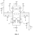
- the ninth switch unit K9 and the tenth switch unit K10 are closed, and the seventh switch unit K7 and the eighth switch unit K8 are disconnected, the fifth switch transistor K32 and the sixth switch transistor K42 are disconnected, and the third switch transistor K31 and the fourth switch transistor K41 are closed, as shown in FIG. 5 .
- the voltage at the first input and output terminal N1 is the sum of the threshold voltage of the second NMOS transistor MN2 and the voltage of the first bit line BLT
- the voltage at the second input and output terminal N2 is the sum of the threshold voltage of the first NMOS transistor NM1 and the voltage of the second bit line BLC.
- the first NMOS transistor MN1 and the second NMOS transistor MN2 are connected in amplification mode to implement amplification of the differential input signal. At this time, the first PMOS transistor MP1 and the second PMOS transistor MP2 are not involved in the amplification process. If the third energy storage unit C3 charges the first bit line BLT in the process of FIG. 4 , the voltage of the first input and output terminal N1 is greater than the voltage of the second input and output terminal N2 in the process in FIG. 5 . If the first bit line BLT charges the third energy storage unit C3 in the process of FIG. 4 , the voltage of the first input and output terminal N1 is less than the voltage of the second input and output terminal N2 in the process of FIG. 5 .
- first switch unit K1 and the second switch unit K2 are closed to connect the first PMOS transistor MP1 and the second PMOS transistor MP2, as shown in FIG. 6 .
- the voltage SAP at the control terminal of the first driving transistor M1 is pulled down to turn on the first driving transistor M1, and the first PMOS transistor MP1 and the second PMOS transistor MP2 are connected into the amplification mode.
- the first PMOS transistor MP1 and the second PMOS transistor MP2 are used to pull up the voltage of the first input and output terminal N1 or the second input and output terminal N2 to the power supply voltage VDD. Specifically, before the process shown in FIG.
- the pull-up by the first PMOS transistor MP1 is enhanced, and the pull-down by the first NMOS transistor MN1 is reduced, so the voltage of the first input and output terminal N1 is pulled up to the power supply voltage VDD; and at the same time, the pull-up by the second PMOS transistor MP2 is reduced, and the pull-down by the second NMOS transistor MN2 is enhanced, so the voltage of the second input and output terminal N2 is pulled down to the ground voltage (GND).
- GDD ground voltage
- the pull-up by the second PMOS transistor MP2 is enhanced, and the pull-down by the second NMOS transistor MN2 is reduced, so the voltage of the second input and output terminal N2 is pulled up to the power supply voltage VDD.
- the pull-up by the first PMOS transistor MP1 is reduced, and the pull-down by the first NMOS transistor MN1 is enhanced, so the voltage of the first input and output terminal N1 is pulled down to the ground voltage.
- the voltage of the first input and output terminal N1 and the voltage of the second input and output terminal N2 have been differentiated by a larger value, that is, the voltage of the first input and output terminal N1 and the voltage of the second input and output terminal N2 are quite different now, and thus the mismatch between the first PMOS transistor MP1 and the second PMOS transistor MP2 is not enough to induce a reading error.
- the write-back stage includes specifically: placing the eleventh switch unit K11 in a closed state to write back to the first bit line BLT. More specifically, the ninth switch unit K9 is disconnected, and the eleventh switch unit K11 is closed, and thus the first input and output terminal N1 charges the third energy storage unit C3 to implement writing back to the first bit line BLT.
Landscapes
- Engineering & Computer Science (AREA)
- Microelectronics & Electronic Packaging (AREA)
- Computer Hardware Design (AREA)
- Dram (AREA)
- Amplifiers (AREA)
Claims (9)
- Leseverstärker umfassend:ein Vorlademodul (11), einen ersten Eingangs- und Ausgangsanschluss (N1), einen zweiten Eingangs- und Ausgangsanschluss (N2), einen ersten Metalloxid-Halbleiter-Transistor mit positivem Kanal, PMOS-Transistor, (MP1), einen zweiten PMOS-Transistor (MP2), einen ersten Metalloxid-Halbleiter-Transistor mit negativem Kanal, NMOS-Transistor, (MN1) einen zweiten NMOS-Transistor (MN2), eine erste Schalteinheit (K1), eine zweite Schalteinheit (K2), eine dritte Schalteinheit (12), eine vierte Schalteinheit (13), eine fünfte Schalteinheit (K5), eine sechste Schalteinheit (K6), eine siebte Schalteinheit (K7), eine achte Schalteinheit (K8), eine erste Energiespeichereinheit (C1), und eine zweite Energiespeichereinheit (C2);wobei ein erstes Ende des Vorlademoduls (11) mit einer ersten Bitleitung (BLT) verbunden ist, und ein zweites Ende des Vorlademoduls (11) mit einer zweiten Bitleitung (BLC) verbunden ist, und wobei das Vorlademodul (11) so konfiguriert ist, dass es die erste Bitleitung (BLT) und die zweite Bitleitung (BLC) auf eine voreingestellte Spannung vorlädt;wobei der erste Eingangs- und Ausgangsanschluss (N1) mit der ersten Bitleitung (BLT) verbunden ist und der zweite Eingangs- und Ausgangsanschluss (N2) mit der zweiten Bitleitung (BLC) verbunden ist;wobei ein Gate des ersten PMOS-Transistors (MP1) über die zweite Schalteinheit (K2) mit dem zweiten Eingangs- und Ausgangsanschluss (N2) verbunden ist, und ein Drain des ersten PMOS-Transistors (MP1) über die erste Schalteinheit (K1) mit dem ersten Eingangs- und Ausgangsanschluss (N1) verbunden ist; wobei ein Gate des zweiten PMOS-Transistors (MP2) über die erste Schalteinheit (K1) mit dem ersten Eingangs- und Ausgangsanschluss (N1) verbunden ist, und ein Drain des zweiten PMOS-Transistors (MP2) über die zweite Schalteinheit (K2) mit dem zweiten Eingangs- und Ausgangsanschluss (N2) verbunden ist; wobei ein Gate des ersten NMOS-Transistors (MN1) mit dem zweiten Eingangs- und Ausgangsanschluss (N2) verbunden ist und ferner über die dritte Schaltereinheit (12) mit dem ersten Eingangs- und Ausgangsanschluss (N1) verbunden ist, und ein Drain des ersten NMOS-Transistors (MN1) über die dritte Schaltereinheit (12) mit dem ersten Eingangs- und Ausgangsanschluss (N1) verbunden ist; wobei ein Gate des zweiten NMOS-Transistors (MN2) mit dem ersten Eingangs- und Ausgangsanschluss (N1) verbunden ist und über die vierte Schalteinheit (13) mit dem zweiten Eingangs- und Ausgangsanschluss (N2) verbunden ist, und ein Drain des zweiten NMOS-Transistors (MN2) über die vierte Schalteinheit (13) mit dem zweiten Eingangs- und Ausgangsanschluss (N2) verbunden ist;wobei ein erstes Ende der fünften Schalteinheit (K5) mit einer Stromversorgungsspannung (VDD) verbunden ist, und ein zweites Ende der fünften Schalteinheit (K5) mit dem ersten Eingangs- und Ausgangsanschluss (N1) verbunden ist;wobei ein erstes Ende der sechsten Schalteinheit (K6) mit der Stromversorgungsspannung (VDD) verbunden ist und das andere Ende der sechsten Schalteinheit (K6) mit dem zweiten Eingangs- und Ausgangsanschluss (N2) verbunden ist;wobei ein erstes Ende der ersten Energiespeichereinheit (C1) mit dem ersten Eingangs- und Ausgangsanschluss (N1) verbunden ist und ein zweites Ende der ersten Energiespeichereinheit (C1) über die siebte Schaltereinheit (K7) geerdet ist;wobei ein erstes Ende der zweiten Energiespeichereinheit (C2) mit dem zweiten Eingangs- und Ausgangsanschluss (N2) verbunden ist und ein zweites Ende der zweiten Energiespeichereinheit (C2) über die achte Schaltereinheit (K8) geerdet ist; undwobei die erste Schalteinheit (K1), die zweite Schalteinheit (K2), die dritte Schalteinheit (12) und die vierte Schalteinheit (13) den ersten PMOS-Transistor (MP1), den zweiten PMOS-Transistor (MP2), den ersten NMOS-Transistor (MN1) und den zweiten NMOS-Transistor (MN2) in einem Verstärkungsmodus oder einem Diodenmodus konfigurieren, wobei der Leseverstärker ferner umfasst: eine neunte Schalteinheit (K9) und eine zehnte Schalteinheit (K10),wobei ein erstes Ende der neunten Schalteinheit (K9) mit der ersten Bitleitung (BLT) verbunden ist, und ein zweites Ende der neunten Schalteinheit (K9) mit dem zweiten Ende der ersten Energiespeichereinheit (C 1) verbunden ist;wobei ein erstes Ende der zehnten Schalteinheit (K10) mit der zweiten Bitleitung (BLC) verbunden ist, und ein zweites Ende der zehnten Schalteinheit (K10) mit dem zweiten Ende der zweiten Energiespeichereinheit (C2) verbunden ist,wobei eine Source des ersten PMOS-Transistors (MP1) und eine Source des zweiten PMOS-Transistors (MP2) so konfiguriert sind, dass sie mit der Stromversorgungsspannung (VDD) verbunden sind, und eine Source des ersten NMOS-Transistors (MN1) und eine Source des zweiten NMOS-Transistors (MN2) so konfiguriert sind, dass sie mit der Masse verbunden sind.
- Leseverstärker nach Anspruch 1 ferner umfassend: eine elfte Schaltereinheit (K11) und eine zwölfte Schaltereinheit (K12),wobei ein erstes Ende der elften Schalteinheit (K11) mit der ersten Bitleitung (BLT) verbunden ist, und ein zweites Ende der elften Schalteinheit (K11) mit dem ersten Eingangs- und Ausgangsanschluss (N1) verbunden ist;wobei ein erstes Ende der zwölften Schalteinheit (K12) mit der zweiten Bitleitung (BLC) verbunden ist, und ein zweites Ende der zwölften Schalteinheit (K12) mit dem zweiten Eingangs- und Ausgangsanschluss (N2) verbunden ist.
- Leseverstärker nach Anspruch 1, ferner umfassend: einen ersten Treibertransistor (M1) und einen zweiten Treibertransistor (M2),wobei ein erstes Ende des ersten Treibertransistors (M1) mit der Versorgungsspannung (VDD) verbunden ist, und ein zweites Ende des ersten Treibertransistors (M1) mit der Source des ersten PMOS-Transistors (MP1) und der Source des zweiten PMOS-Transistors (MP2) verbunden ist;wobei ein erstes Ende des zweiten Treibertransistors (M2) geerdet ist, und ein zweites Ende des zweiten Treibertransistors (M2) mit der Source des ersten NMOS-Transistors (MN 1) und der Source des zweiten NMOS-Transistors (MN2) verbunden ist.
- Leseverstärker nach Anspruch 3, wobei der erste Treibertransistor (M1) einen PMOS-Transistor umfasst, eine Source des ersten Treibertransistors (M1) mit der Stromversorgungsspannung (VDD) verbunden ist und ein Drain des ersten Treibertransistors (M1) mit der Source des ersten PMOS-Transistors (MP1) und der Source des zweiten PMOS-Transistors (MP2) verbunden ist;
wobei der zweite Treibertransistor (M2) einen NMOS-Transistor umfasst, eine Source des zweiten Treibertransistors (M2) geerdet ist, und ein Drain des zweiten Treibertransistors (M2) mit der Source des ersten NMOS-Transistors (MN1) und der Source des zweiten NMOS-Transistors (MN2) verbunden ist. - Leseverstärker nach Anspruch 1 ferner umfassen: einen ersten Schalttransistor (M3), einen zweiten Schalttransistor (M4), eine dritte Energiespeichereinheit (C3) und eine vierte Energiespeichereinheit (C4);wobei ein erstes Ende des ersten Schalttransistors (M3) mit der ersten Bitleitung (BLT) verbunden ist, ein zweites Ende des ersten Schalttransistors (M3) mit einem ersten Ende der dritten Energiespeichereinheit (C3) verbunden ist und ein zweites Ende der dritten Energiespeichereinheit (C3) geerdet ist;wobei ein erstes Ende des zweiten Schalttransistors (M4) mit der zweiten Bitleitung (BLC) verbunden ist, und ein zweites Ende des zweiten Schalttransistors (M4) mit einem ersten Ende der vierten Energiespeichereinheit (C4) verbunden ist, und ein zweites Ende der vierten Energiespeichereinheit (C4) geerdet ist.
- Leseverstärker nach Anspruch 5, wobei die dritte Schalteinheit (12) einen dritten Schalttransistor (K31) und einen fünften Schalttransistor (K32) umfasst, und die vierte Schalteinheit (13) einen vierten Schalttransistor (K41) und einen sechsten Schalttransistor (K42) umfasst;wobei ein Ende des dritten Schalttransistors (K31) mit dem ersten Eingangs- und Ausgangsanschluss (N1) verbunden ist, das andere Ende des dritten Schalttransistors (K31) mit dem Drain des ersten NMOS-Transistors (MN1) verbunden ist; undwobei ein erstes Ende des fünften Schalttransistors (K32) mit dem Drain des ersten NMOS-Transistors (MN1) verbunden ist, und ein zweites Ende des fünften Schalttransistors (K32) mit einem Gate des ersten NMOS-Transistors (MN1) verbunden ist;wobei ein erstes Ende des vierten Schalttransistors (K41) mit dem zweiten Eingangs- und Ausgangsanschluss (N2) verbunden ist, ein zweites Ende des vierten Schalttransistors (K41) mit dem Drain des zweiten NMOS-Transistors (MN2) verbunden ist; undwobei ein erstes Ende des sechsten Schalttransistors (K42) mit dem Drain des zweiten NMOS-Transistors (MN2) verbunden ist, und ein zweites Ende des sechsten Schalttransistors (K42) mit dem Gate des zweiten NMOS-Transistors (MN2) verbunden ist.
- Leseverstärker nach Anspruch 6, wobei der dritte Schalttransistor (K31), der vierte Schalttransistor (K41), der fünfte Schalttransistor (K32) und der sechste Schalttransistor (K42) entweder NMOS-Transistoren oder aus NMOS-Transistoren und PMOS-Transistoren zusammengesetzte Übertragungsgates sind.
- Verfahren zur Steuerung eines Leseverstärkers nach einem der Ansprüche 1 bis 7, umfassend:in einer Vorladestufe Vorladen der ersten Bitleitung (BLT) und der zweiten Bitleitung (BLC) auf die voreingestellte Spannung; undin einer Offset-Spannungskompensationsstufe Einstellen eines Verbindungsmodus des ersten PMOS-Transistors (MP1), des zweiten PMOS-Transistors (MP2), des zweiten NMOS-Transistors (MN2) und des zweiten NMOS-Transistors (MN2), um eine Offset-Spannungsdifferenz zwischen dem ersten Eingangs- und Ausgangsanschluss (N1) und dem zweiten Eingangs- und Ausgangsanschluss (N2) zu kompensieren,wobei das Steuerverfahren in der Offset-Spannungskompensationsstufe insbesondere umfasst:Versetzen wenigstens der ersten Schalteinheit (K1), der zweiten Schalteinheit (K2), der dritten Schalteinheit (12) und der vierten Schalteinheit (13) in einen Aus-Zustand und Versetzen der fünften Schalteinheit (K5), der sechsten Schalteinheit (K6), der siebten Schalteinheit (K7) und der achten Schalteinheit (K8) in einen Ein-Zustand, so dass der erste Eingangs- und Ausgangsanschluss (N1) und der zweite Eingangs- und Ausgangsanschluss (N2) auf die Stromversorgungsspannung (VDD) aufgeladen werden;Versetzen der fünften Schaltereinheit (K5) und der sechsten Schaltereinheit (K6) in den Aus-Zustand, Kurzschließen eines Gates des ersten NMOS-Transistors (MN1) und des Drains des ersten NMOS-Transistors (MN1) und Kurzschließen eines Gates des zweiten NMOS-Transistors (MN2) und eines Drains des zweiten NMOS-Transistors (MN2), um eine Spannung des ersten Eingangs- und Ausgangsanschlusses (N1) auf eine Schwellenspannung des zweiten NMOS-Transistors (MN2) zu entladen, und um eine Spannung des zweiten Eingangs- und Ausgangsanschlusses (N2) auf eine Schwellenspannung des ersten NMOS-Transistors (MN1) zu entladen.
- Steuerverfahren für den Leseverstärker nach Anspruch 8, wobei das Verfahren nach der Offset-Spannungskompensationsstufe ferner umfasst:in einer Kleinsignalverstärkungsstufe, Verbinden des ersten NMOS-Transistors (MN1) und des zweiten NMOS-Transistors (MN2) in einem Verstärkungsmodus und Verstärken der Offset-Spannungsdifferenz zwischen dem ersten Eingangs- und Ausgangsanschluss (N1) und dem zweiten Eingangs- und Ausgangsanschluss (N2); und Verbinden des ersten PMOS-Transistors (MP1) und des zweiten PMOS-Transistors (MP2) in einem Verstärkungsmodus; und Hochziehen einer Spannung des ersten Eingangs- und Ausgangsanschlusses (N1) oder einer Spannung des zweiten Eingangs- und Ausgangsanschlusses (N2) auf die Stromversorgungsspannung (VDD); undin einer Write-Back-Stufe, wobei in die erste Bitleitung (BLT) zurückgeschrieben wird.
Applications Claiming Priority (2)
| Application Number | Priority Date | Filing Date | Title |
|---|---|---|---|
| CN201911188084.5A CN112863561B (zh) | 2019-11-28 | 2019-11-28 | 灵敏放大器及其控制方法 |
| PCT/CN2020/097046 WO2021103501A1 (zh) | 2019-11-28 | 2020-06-19 | 灵敏放大器及其控制方法 |
Publications (3)
| Publication Number | Publication Date |
|---|---|
| EP3920185A1 EP3920185A1 (de) | 2021-12-08 |
| EP3920185A4 EP3920185A4 (de) | 2022-05-25 |
| EP3920185B1 true EP3920185B1 (de) | 2023-05-31 |
Family
ID=75985246
Family Applications (1)
| Application Number | Title | Priority Date | Filing Date |
|---|---|---|---|
| EP20893181.6A Active EP3920185B1 (de) | 2019-11-28 | 2020-06-19 | Empfindlicher verstärker und steuerungsverfahren dafür |
Country Status (4)
| Country | Link |
|---|---|
| US (1) | US11790959B2 (de) |
| EP (1) | EP3920185B1 (de) |
| CN (1) | CN112863561B (de) |
| WO (1) | WO2021103501A1 (de) |
Families Citing this family (7)
| Publication number | Priority date | Publication date | Assignee | Title |
|---|---|---|---|---|
| CN112863561B (zh) | 2019-11-28 | 2024-05-03 | 长鑫存储技术有限公司 | 灵敏放大器及其控制方法 |
| EP4148580B1 (de) * | 2021-07-16 | 2025-07-16 | Changxin Memory Technologies, Inc. | Empfänger, speicher und testverfahren |
| CN116168737B (zh) * | 2021-11-24 | 2024-05-14 | 长鑫存储技术有限公司 | 感测放大电路以及数据读出方法 |
| US12112824B2 (en) | 2021-11-24 | 2024-10-08 | Changxin Memory Technologies, Inc. | Sense amplifier circuit and data read method |
| US12100441B2 (en) * | 2022-01-14 | 2024-09-24 | Changxin Memory Technologies, Inc. | Readout circuit layout and sense amplification circuit |
| KR20230167612A (ko) * | 2022-06-02 | 2023-12-11 | 삼성전자주식회사 | 반도체 메모리 장치의 비트라인 센스앰프 및 비트라인 센싱방법 |
| CN117497023B (zh) * | 2023-11-03 | 2024-05-03 | 北京超弦存储器研究院 | 感应放大器及其控制方法、存储阵列结构及存储器 |
Family Cites Families (25)
| Publication number | Priority date | Publication date | Assignee | Title |
|---|---|---|---|---|
| US5499218A (en) * | 1995-01-31 | 1996-03-12 | Goldstar Electron Co., Ltd. | Method for driving bit line selecting signals |
| KR20000065800A (ko) * | 1999-04-09 | 2000-11-15 | 윤종용 | 차동 센스증폭기의 오프셋 전압 보상 회로 |
| DE10022263A1 (de) * | 2000-05-08 | 2001-11-22 | Infineon Technologies Ag | Speicher-Leseverstärker |
| US20070024325A1 (en) * | 2005-08-01 | 2007-02-01 | Chung-Kuang Chen | Sense amplifier with input offset compensation |
| US7916556B2 (en) * | 2007-01-09 | 2011-03-29 | Sony Corporation | Semiconductor memory device, sense amplifier circuit and memory cell reading method using a threshold correction circuitry |
| JP2011248971A (ja) * | 2010-05-28 | 2011-12-08 | Elpida Memory Inc | 半導体装置 |
| CN101916583B (zh) * | 2010-07-30 | 2015-12-09 | 上海华虹宏力半导体制造有限公司 | 灵敏放大器以及存储器 |
| KR101858579B1 (ko) * | 2011-04-29 | 2018-05-17 | 에스케이하이닉스 주식회사 | 센스 앰프 회로 |
| JP2014102870A (ja) * | 2012-11-21 | 2014-06-05 | Toshiba Corp | センスアンプ回路 |
| US8830766B2 (en) * | 2013-01-23 | 2014-09-09 | Lsi Corporation | Margin free PVT tolerant fast self-timed sense amplifier reset circuit |
| CN104036821B (zh) * | 2014-06-12 | 2017-03-22 | 江南大学 | 一种改进型交叉耦合灵敏放大器 |
| US9286969B2 (en) * | 2014-06-27 | 2016-03-15 | Globalfoundries Inc. | Low power sense amplifier for static random access memory |
| CN104269189B (zh) | 2014-10-27 | 2017-12-08 | 北海市蕴芯电子科技有限公司 | 一种微功耗eeprom灵敏放大器电路 |
| US9437282B1 (en) * | 2015-08-06 | 2016-09-06 | Globalfoundries Inc. | High performance sense amplifier |
| US11074988B2 (en) * | 2016-03-22 | 2021-07-27 | Micron Technology, Inc. | Apparatus and methods for debugging on a host and memory device |
| CN105895139B (zh) | 2016-03-30 | 2018-04-17 | 上海华虹宏力半导体制造有限公司 | 灵敏放大器 |
| CN106205664B (zh) * | 2016-06-28 | 2017-05-17 | 湖南恒茂高科股份有限公司 | 存储器读写传输门管控电路 |
| KR102319827B1 (ko) * | 2017-06-28 | 2021-11-01 | 에스케이하이닉스 주식회사 | 증폭기 회로 |
| CN108231100B (zh) * | 2018-03-26 | 2023-09-19 | 安徽大学 | 失调电压自适应数字校准型灵敏放大器 |
| CN108648775B (zh) * | 2018-05-07 | 2023-10-20 | 长鑫存储技术有限公司 | 灵敏放大器、半导体存储装置及电压差的放大方法 |
| CN109166598B (zh) | 2018-08-17 | 2024-02-06 | 长鑫存储技术有限公司 | 灵敏放大器电路、存储器及信号放大方法 |
| US10762953B2 (en) * | 2018-12-13 | 2020-09-01 | International Business Machines Corporation | Memory array with reduced circuitry |
| CN109841240B (zh) * | 2018-12-21 | 2020-10-16 | 北京时代民芯科技有限公司 | 一种sram型存储器高速灵敏放大器电路 |
| CN112863561B (zh) | 2019-11-28 | 2024-05-03 | 长鑫存储技术有限公司 | 灵敏放大器及其控制方法 |
| CN210575115U (zh) * | 2019-11-28 | 2020-05-19 | 长鑫存储技术有限公司 | 灵敏放大器 |
-
2019
- 2019-11-28 CN CN201911188084.5A patent/CN112863561B/zh active Active
-
2020
- 2020-06-19 US US17/430,709 patent/US11790959B2/en active Active
- 2020-06-19 WO PCT/CN2020/097046 patent/WO2021103501A1/zh not_active Ceased
- 2020-06-19 EP EP20893181.6A patent/EP3920185B1/de active Active
Also Published As
| Publication number | Publication date |
|---|---|
| CN112863561B (zh) | 2024-05-03 |
| CN112863561A (zh) | 2021-05-28 |
| US20220148628A1 (en) | 2022-05-12 |
| US11790959B2 (en) | 2023-10-17 |
| EP3920185A1 (de) | 2021-12-08 |
| WO2021103501A1 (zh) | 2021-06-03 |
| EP3920185A4 (de) | 2022-05-25 |
Similar Documents
| Publication | Publication Date | Title |
|---|---|---|
| EP3920185B1 (de) | Empfindlicher verstärker und steuerungsverfahren dafür | |
| CN210575115U (zh) | 灵敏放大器 | |
| US8588019B2 (en) | Semiconductor device having current change memory cell | |
| US7616511B2 (en) | Input/output line sense amplifier and semiconductor memory device using the same | |
| EP3926628A1 (de) | Leseverstärker, speicher und datenausleseverfahren | |
| US11869624B2 (en) | Sense amplifier, memory and method for controlling sense amplifier | |
| US20130010561A1 (en) | Sense amplifiers and exemplary applications | |
| KR20100097891A (ko) | 비휘발성 메모리 장치 및 이를 위한 바이어스 생성 회로 | |
| US20140062531A1 (en) | Signal driver circuit having adjustable output voltage for a high logic level output signal | |
| JPS6069898A (ja) | 半導体記憶装置 | |
| US8125840B2 (en) | Reference level generation with offset compensation for sense amplifier | |
| US8687448B2 (en) | Semiconductor memory device and sense amplifier | |
| US6239624B1 (en) | Low-power sense amplifier for memory | |
| US6728151B2 (en) | Driving a DRAM sense amplifier having low threshold voltage PMOS transistors | |
| US20090146697A1 (en) | Circuit for buffering having a coupler | |
| US20220029586A1 (en) | Sense amplifier, memory and method for controlling sense amplifier | |
| KR100925368B1 (ko) | 센스앰프 전압 공급 회로 및 그의 구동 방법 | |
| TWI573389B (zh) | 發信號系統、前置放大器、記憶體裝置及方法 | |
| US6456120B1 (en) | Capacitor-coupling differential logic circuit | |
| US7869292B2 (en) | Dynamic type semiconductor memory device and operation method of the same | |
| US10726900B2 (en) | Semiconductor memory device and method for reading semiconductor memory device | |
| CN103077740A (zh) | 带补偿电路的电流模式灵敏放大器及使用方法 | |
| US8995219B2 (en) | Word line driver | |
| US6917550B2 (en) | Semiconductor memory device | |
| WO2009157489A1 (ja) | 半導体記憶装置のセンスアンプ回路 |
Legal Events
| Date | Code | Title | Description |
|---|---|---|---|
| STAA | Information on the status of an ep patent application or granted ep patent |
Free format text: STATUS: THE INTERNATIONAL PUBLICATION HAS BEEN MADE |
|
| PUAI | Public reference made under article 153(3) epc to a published international application that has entered the european phase |
Free format text: ORIGINAL CODE: 0009012 |
|
| STAA | Information on the status of an ep patent application or granted ep patent |
Free format text: STATUS: REQUEST FOR EXAMINATION WAS MADE |
|
| 17P | Request for examination filed |
Effective date: 20210903 |
|
| AK | Designated contracting states |
Kind code of ref document: A1 Designated state(s): AL AT BE BG CH CY CZ DE DK EE ES FI FR GB GR HR HU IE IS IT LI LT LU LV MC MK MT NL NO PL PT RO RS SE SI SK SM TR |
|
| A4 | Supplementary search report drawn up and despatched |
Effective date: 20220428 |
|
| RIC1 | Information provided on ipc code assigned before grant |
Ipc: G11C 7/02 20060101ALI20220421BHEP Ipc: G11C 11/4091 20060101ALI20220421BHEP Ipc: G11C 7/12 20060101ALI20220421BHEP Ipc: G11C 7/08 20060101ALI20220421BHEP Ipc: G11C 7/10 20060101ALI20220421BHEP Ipc: G11C 7/06 20060101AFI20220421BHEP |
|
| GRAP | Despatch of communication of intention to grant a patent |
Free format text: ORIGINAL CODE: EPIDOSNIGR1 |
|
| STAA | Information on the status of an ep patent application or granted ep patent |
Free format text: STATUS: GRANT OF PATENT IS INTENDED |
|
| DAV | Request for validation of the european patent (deleted) | ||
| DAX | Request for extension of the european patent (deleted) | ||
| INTG | Intention to grant announced |
Effective date: 20230213 |
|
| GRAS | Grant fee paid |
Free format text: ORIGINAL CODE: EPIDOSNIGR3 |
|
| GRAA | (expected) grant |
Free format text: ORIGINAL CODE: 0009210 |
|
| STAA | Information on the status of an ep patent application or granted ep patent |
Free format text: STATUS: THE PATENT HAS BEEN GRANTED |
|
| AK | Designated contracting states |
Kind code of ref document: B1 Designated state(s): AL AT BE BG CH CY CZ DE DK EE ES FI FR GB GR HR HU IE IS IT LI LT LU LV MC MK MT NL NO PL PT RO RS SE SI SK SM TR |
|
| REG | Reference to a national code |
Ref country code: GB Ref legal event code: FG4D Ref country code: CH Ref legal event code: EP |
|
| REG | Reference to a national code |
Ref country code: DE Ref legal event code: R096 Ref document number: 602020011402 Country of ref document: DE |
|
| REG | Reference to a national code |
Ref country code: AT Ref legal event code: REF Ref document number: 1571437 Country of ref document: AT Kind code of ref document: T Effective date: 20230615 |
|
| REG | Reference to a national code |
Ref country code: IE Ref legal event code: FG4D |
|
| REG | Reference to a national code |
Ref country code: NL Ref legal event code: FP |
|
| P01 | Opt-out of the competence of the unified patent court (upc) registered |
Effective date: 20230530 |
|
| REG | Reference to a national code |
Ref country code: LT Ref legal event code: MG9D |
|
| REG | Reference to a national code |
Ref country code: AT Ref legal event code: MK05 Ref document number: 1571437 Country of ref document: AT Kind code of ref document: T Effective date: 20230531 |
|
| PG25 | Lapsed in a contracting state [announced via postgrant information from national office to epo] |
Ref country code: SE Free format text: LAPSE BECAUSE OF FAILURE TO SUBMIT A TRANSLATION OF THE DESCRIPTION OR TO PAY THE FEE WITHIN THE PRESCRIBED TIME-LIMIT Effective date: 20230531 Ref country code: NO Free format text: LAPSE BECAUSE OF FAILURE TO SUBMIT A TRANSLATION OF THE DESCRIPTION OR TO PAY THE FEE WITHIN THE PRESCRIBED TIME-LIMIT Effective date: 20230831 Ref country code: ES Free format text: LAPSE BECAUSE OF FAILURE TO SUBMIT A TRANSLATION OF THE DESCRIPTION OR TO PAY THE FEE WITHIN THE PRESCRIBED TIME-LIMIT Effective date: 20230531 Ref country code: AT Free format text: LAPSE BECAUSE OF FAILURE TO SUBMIT A TRANSLATION OF THE DESCRIPTION OR TO PAY THE FEE WITHIN THE PRESCRIBED TIME-LIMIT Effective date: 20230531 |
|
| PG25 | Lapsed in a contracting state [announced via postgrant information from national office to epo] |
Ref country code: RS Free format text: LAPSE BECAUSE OF FAILURE TO SUBMIT A TRANSLATION OF THE DESCRIPTION OR TO PAY THE FEE WITHIN THE PRESCRIBED TIME-LIMIT Effective date: 20230531 Ref country code: PL Free format text: LAPSE BECAUSE OF FAILURE TO SUBMIT A TRANSLATION OF THE DESCRIPTION OR TO PAY THE FEE WITHIN THE PRESCRIBED TIME-LIMIT Effective date: 20230531 Ref country code: LV Free format text: LAPSE BECAUSE OF FAILURE TO SUBMIT A TRANSLATION OF THE DESCRIPTION OR TO PAY THE FEE WITHIN THE PRESCRIBED TIME-LIMIT Effective date: 20230531 Ref country code: LT Free format text: LAPSE BECAUSE OF FAILURE TO SUBMIT A TRANSLATION OF THE DESCRIPTION OR TO PAY THE FEE WITHIN THE PRESCRIBED TIME-LIMIT Effective date: 20230531 Ref country code: IS Free format text: LAPSE BECAUSE OF FAILURE TO SUBMIT A TRANSLATION OF THE DESCRIPTION OR TO PAY THE FEE WITHIN THE PRESCRIBED TIME-LIMIT Effective date: 20230930 Ref country code: HR Free format text: LAPSE BECAUSE OF FAILURE TO SUBMIT A TRANSLATION OF THE DESCRIPTION OR TO PAY THE FEE WITHIN THE PRESCRIBED TIME-LIMIT Effective date: 20230531 Ref country code: GR Free format text: LAPSE BECAUSE OF FAILURE TO SUBMIT A TRANSLATION OF THE DESCRIPTION OR TO PAY THE FEE WITHIN THE PRESCRIBED TIME-LIMIT Effective date: 20230901 |
|
| PG25 | Lapsed in a contracting state [announced via postgrant information from national office to epo] |
Ref country code: FI Free format text: LAPSE BECAUSE OF FAILURE TO SUBMIT A TRANSLATION OF THE DESCRIPTION OR TO PAY THE FEE WITHIN THE PRESCRIBED TIME-LIMIT Effective date: 20230531 |
|
| PG25 | Lapsed in a contracting state [announced via postgrant information from national office to epo] |
Ref country code: SK Free format text: LAPSE BECAUSE OF FAILURE TO SUBMIT A TRANSLATION OF THE DESCRIPTION OR TO PAY THE FEE WITHIN THE PRESCRIBED TIME-LIMIT Effective date: 20230531 |
|
| PG25 | Lapsed in a contracting state [announced via postgrant information from national office to epo] |
Ref country code: SM Free format text: LAPSE BECAUSE OF FAILURE TO SUBMIT A TRANSLATION OF THE DESCRIPTION OR TO PAY THE FEE WITHIN THE PRESCRIBED TIME-LIMIT Effective date: 20230531 Ref country code: SK Free format text: LAPSE BECAUSE OF FAILURE TO SUBMIT A TRANSLATION OF THE DESCRIPTION OR TO PAY THE FEE WITHIN THE PRESCRIBED TIME-LIMIT Effective date: 20230531 Ref country code: RO Free format text: LAPSE BECAUSE OF FAILURE TO SUBMIT A TRANSLATION OF THE DESCRIPTION OR TO PAY THE FEE WITHIN THE PRESCRIBED TIME-LIMIT Effective date: 20230531 Ref country code: PT Free format text: LAPSE BECAUSE OF FAILURE TO SUBMIT A TRANSLATION OF THE DESCRIPTION OR TO PAY THE FEE WITHIN THE PRESCRIBED TIME-LIMIT Effective date: 20231002 Ref country code: EE Free format text: LAPSE BECAUSE OF FAILURE TO SUBMIT A TRANSLATION OF THE DESCRIPTION OR TO PAY THE FEE WITHIN THE PRESCRIBED TIME-LIMIT Effective date: 20230531 Ref country code: DK Free format text: LAPSE BECAUSE OF FAILURE TO SUBMIT A TRANSLATION OF THE DESCRIPTION OR TO PAY THE FEE WITHIN THE PRESCRIBED TIME-LIMIT Effective date: 20230531 Ref country code: CZ Free format text: LAPSE BECAUSE OF FAILURE TO SUBMIT A TRANSLATION OF THE DESCRIPTION OR TO PAY THE FEE WITHIN THE PRESCRIBED TIME-LIMIT Effective date: 20230531 |
|
| REG | Reference to a national code |
Ref country code: CH Ref legal event code: PL |
|
| REG | Reference to a national code |
Ref country code: BE Ref legal event code: MM Effective date: 20230630 |
|
| PG25 | Lapsed in a contracting state [announced via postgrant information from national office to epo] |
Ref country code: MC Free format text: LAPSE BECAUSE OF FAILURE TO SUBMIT A TRANSLATION OF THE DESCRIPTION OR TO PAY THE FEE WITHIN THE PRESCRIBED TIME-LIMIT Effective date: 20230531 |
|
| PG25 | Lapsed in a contracting state [announced via postgrant information from national office to epo] |
Ref country code: MC Free format text: LAPSE BECAUSE OF FAILURE TO SUBMIT A TRANSLATION OF THE DESCRIPTION OR TO PAY THE FEE WITHIN THE PRESCRIBED TIME-LIMIT Effective date: 20230531 |
|
| PG25 | Lapsed in a contracting state [announced via postgrant information from national office to epo] |
Ref country code: LU Free format text: LAPSE BECAUSE OF NON-PAYMENT OF DUE FEES Effective date: 20230619 |
|
| REG | Reference to a national code |
Ref country code: DE Ref legal event code: R097 Ref document number: 602020011402 Country of ref document: DE |
|
| REG | Reference to a national code |
Ref country code: IE Ref legal event code: MM4A |
|
| PG25 | Lapsed in a contracting state [announced via postgrant information from national office to epo] |
Ref country code: LU Free format text: LAPSE BECAUSE OF NON-PAYMENT OF DUE FEES Effective date: 20230619 |
|
| PLBE | No opposition filed within time limit |
Free format text: ORIGINAL CODE: 0009261 |
|
| STAA | Information on the status of an ep patent application or granted ep patent |
Free format text: STATUS: NO OPPOSITION FILED WITHIN TIME LIMIT |
|
| PG25 | Lapsed in a contracting state [announced via postgrant information from national office to epo] |
Ref country code: IE Free format text: LAPSE BECAUSE OF NON-PAYMENT OF DUE FEES Effective date: 20230619 |
|
| PG25 | Lapsed in a contracting state [announced via postgrant information from national office to epo] |
Ref country code: IE Free format text: LAPSE BECAUSE OF NON-PAYMENT OF DUE FEES Effective date: 20230619 Ref country code: CH Free format text: LAPSE BECAUSE OF NON-PAYMENT OF DUE FEES Effective date: 20230630 |
|
| PG25 | Lapsed in a contracting state [announced via postgrant information from national office to epo] |
Ref country code: SI Free format text: LAPSE BECAUSE OF FAILURE TO SUBMIT A TRANSLATION OF THE DESCRIPTION OR TO PAY THE FEE WITHIN THE PRESCRIBED TIME-LIMIT Effective date: 20230531 |
|
| 26N | No opposition filed |
Effective date: 20240301 |
|
| PG25 | Lapsed in a contracting state [announced via postgrant information from national office to epo] |
Ref country code: SI Free format text: LAPSE BECAUSE OF FAILURE TO SUBMIT A TRANSLATION OF THE DESCRIPTION OR TO PAY THE FEE WITHIN THE PRESCRIBED TIME-LIMIT Effective date: 20230531 Ref country code: IT Free format text: LAPSE BECAUSE OF FAILURE TO SUBMIT A TRANSLATION OF THE DESCRIPTION OR TO PAY THE FEE WITHIN THE PRESCRIBED TIME-LIMIT Effective date: 20230531 Ref country code: BE Free format text: LAPSE BECAUSE OF NON-PAYMENT OF DUE FEES Effective date: 20230630 |
|
| PG25 | Lapsed in a contracting state [announced via postgrant information from national office to epo] |
Ref country code: BG Free format text: LAPSE BECAUSE OF FAILURE TO SUBMIT A TRANSLATION OF THE DESCRIPTION OR TO PAY THE FEE WITHIN THE PRESCRIBED TIME-LIMIT Effective date: 20230531 |
|
| PG25 | Lapsed in a contracting state [announced via postgrant information from national office to epo] |
Ref country code: BG Free format text: LAPSE BECAUSE OF FAILURE TO SUBMIT A TRANSLATION OF THE DESCRIPTION OR TO PAY THE FEE WITHIN THE PRESCRIBED TIME-LIMIT Effective date: 20230531 |
|
| PGFP | Annual fee paid to national office [announced via postgrant information from national office to epo] |
Ref country code: DE Payment date: 20250618 Year of fee payment: 6 |
|
| PGFP | Annual fee paid to national office [announced via postgrant information from national office to epo] |
Ref country code: GB Payment date: 20250618 Year of fee payment: 6 |
|
| PGFP | Annual fee paid to national office [announced via postgrant information from national office to epo] |
Ref country code: NL Payment date: 20250618 Year of fee payment: 6 |
|
| PGFP | Annual fee paid to national office [announced via postgrant information from national office to epo] |
Ref country code: FR Payment date: 20250627 Year of fee payment: 6 |
|
| PG25 | Lapsed in a contracting state [announced via postgrant information from national office to epo] |
Ref country code: CY Free format text: LAPSE BECAUSE OF FAILURE TO SUBMIT A TRANSLATION OF THE DESCRIPTION OR TO PAY THE FEE WITHIN THE PRESCRIBED TIME-LIMIT; INVALID AB INITIO Effective date: 20200619 |
|
| PG25 | Lapsed in a contracting state [announced via postgrant information from national office to epo] |
Ref country code: HU Free format text: LAPSE BECAUSE OF FAILURE TO SUBMIT A TRANSLATION OF THE DESCRIPTION OR TO PAY THE FEE WITHIN THE PRESCRIBED TIME-LIMIT; INVALID AB INITIO Effective date: 20200619 |
|
| PG25 | Lapsed in a contracting state [announced via postgrant information from national office to epo] |
Ref country code: TR Free format text: LAPSE BECAUSE OF FAILURE TO SUBMIT A TRANSLATION OF THE DESCRIPTION OR TO PAY THE FEE WITHIN THE PRESCRIBED TIME-LIMIT Effective date: 20230531 |