EP3909050B1 - Verfahren zur programmierung einer mehrstufigen nand-flash-speichervorrichtung und mlc-nand-flash-speichervorrichtung - Google Patents
Verfahren zur programmierung einer mehrstufigen nand-flash-speichervorrichtung und mlc-nand-flash-speichervorrichtung Download PDFInfo
- Publication number
- EP3909050B1 EP3909050B1 EP19929556.9A EP19929556A EP3909050B1 EP 3909050 B1 EP3909050 B1 EP 3909050B1 EP 19929556 A EP19929556 A EP 19929556A EP 3909050 B1 EP3909050 B1 EP 3909050B1
- Authority
- EP
- European Patent Office
- Prior art keywords
- verification
- predetermined page
- controller
- programming voltage
- flash memory
- Prior art date
- Legal status (The legal status is an assumption and is not a legal conclusion. Google has not performed a legal analysis and makes no representation as to the accuracy of the status listed.)
- Active
Links
Images



Classifications
-
- G—PHYSICS
- G11—INFORMATION STORAGE
- G11C—STATIC STORES
- G11C11/00—Digital stores characterised by the use of particular electric or magnetic storage elements; Storage elements therefor
- G11C11/56—Digital stores characterised by the use of particular electric or magnetic storage elements; Storage elements therefor using storage elements with more than two stable states represented by steps, e.g. of voltage, current, phase, frequency
- G11C11/5621—Digital stores characterised by the use of particular electric or magnetic storage elements; Storage elements therefor using storage elements with more than two stable states represented by steps, e.g. of voltage, current, phase, frequency using charge storage in a floating gate
- G11C11/5628—Programming or writing circuits; Data input circuits
-
- G—PHYSICS
- G11—INFORMATION STORAGE
- G11C—STATIC STORES
- G11C16/00—Erasable programmable read-only memories
- G11C16/02—Erasable programmable read-only memories electrically programmable
- G11C16/06—Auxiliary circuits, e.g. for writing into memory
- G11C16/10—Programming or data input circuits
-
- G—PHYSICS
- G11—INFORMATION STORAGE
- G11C—STATIC STORES
- G11C16/00—Erasable programmable read-only memories
- G11C16/02—Erasable programmable read-only memories electrically programmable
- G11C16/06—Auxiliary circuits, e.g. for writing into memory
- G11C16/10—Programming or data input circuits
- G11C16/12—Programming voltage switching circuits
-
- G—PHYSICS
- G11—INFORMATION STORAGE
- G11C—STATIC STORES
- G11C16/00—Erasable programmable read-only memories
- G11C16/02—Erasable programmable read-only memories electrically programmable
- G11C16/06—Auxiliary circuits, e.g. for writing into memory
- G11C16/26—Sensing or reading circuits; Data output circuits
-
- G—PHYSICS
- G11—INFORMATION STORAGE
- G11C—STATIC STORES
- G11C16/00—Erasable programmable read-only memories
- G11C16/02—Erasable programmable read-only memories electrically programmable
- G11C16/06—Auxiliary circuits, e.g. for writing into memory
- G11C16/34—Determination of programming status, e.g. threshold voltage, overprogramming or underprogramming, retention
- G11C16/3436—Arrangements for verifying correct programming or erasure
- G11C16/3454—Arrangements for verifying correct programming or for detecting overprogrammed cells
- G11C16/3459—Circuits or methods to verify correct programming of nonvolatile memory cells
-
- G—PHYSICS
- G11—INFORMATION STORAGE
- G11C—STATIC STORES
- G11C16/00—Erasable programmable read-only memories
- G11C16/02—Erasable programmable read-only memories electrically programmable
- G11C16/04—Erasable programmable read-only memories electrically programmable using variable threshold transistors, e.g. FAMOS
- G11C16/0483—Erasable programmable read-only memories electrically programmable using variable threshold transistors, e.g. FAMOS comprising cells having several storage transistors connected in series
-
- G—PHYSICS
- G11—INFORMATION STORAGE
- G11C—STATIC STORES
- G11C2211/00—Indexing scheme relating to digital stores characterized by the use of particular electric or magnetic storage elements; Storage elements therefor
- G11C2211/56—Indexing scheme relating to G11C11/56 and sub-groups for features not covered by these groups
- G11C2211/562—Multilevel memory programming aspects
- G11C2211/5621—Multilevel programming verification
Definitions
- the invention relates to semiconductor devices, and specifically, to a method of programming a multilevel cell (MLC) NAND flash memory device and an MLC NAND flash memory device.
- MLC multilevel cell
- NAND Flash memories are widely adopted for non-volatile data storage in mobile devices and consumer electronics, and store data in an array of memory cells by programming the memory cells into different program states.
- SLC single level cell
- MLC multi-level cell
- Flash memory may employ several read levels corresponding to the different program states to read data from the memory cells.
- memory cells may be set to various program states by applying corresponding programming voltages thereto.
- US 2012/0236654 A1 and US 2010/0182839 A1 discloses processes for a plurality of non-volatile storage elements to increase the speed of programming.
- the memory cells may degrade and shifts of the programming voltages may occur over time. As a result, it is important to determine the programming voltages, and especially a start programming pulse of a flash memory prior to programming.
- ISPP Incremental Step Pulse Programming
- a series of programming pulses are applied to select memory cells to gradually raise the threshold voltage of the memory cells to above a specific threshold level, and upon reaching the specific threshold level a programming voltage can be identified.
- the shift of the programming voltage is large, it might take a long time for ISPP to detect programming voltages as a large number of programming pulses has to be applied to memory cells in order to establish the required threshold voltage.
- the invention is defined in independent method claim 1 and independent apparatus claim 6.
- a method of programming a NAND flash memory device includes: a programming voltage generation circuit applying an initial programming voltage pulse to a predetermined page of NAND flash memory; a controller verifying a plurality of verification levels of the predetermined page, the plurality of verification levels being less than a first-state verification voltage of reading a lowest program state of the predetermined page; the controller determining a magnitude of a subsequent programming voltage pulse upon one of the plurality of verification levels of the predetermined page passing a verification; and the programming voltage generation circuit applying the subsequent programming voltage pulse to the predetermined page or other pages in the NAND flash memory; the controller adjusting when to verify a higher-state verification voltage (Vpg(n)) according to a number of failed verifications of the plurality of verification levels of the predetermined page, wherein preferably the controller adjusting when to verify the higher-state verification voltage comprises: the controller configuring a start step pulse count for starting a verification of the higher-state verification voltage (Vpg(n)); and the controller incrementing the start step pulse count
- a NAND flash memory device in another embodiment, includes NAND flash memory, a programming voltage generation circuit and a controller.
- the NAND flash memory includes a predetermined page and other pages.
- the programming voltage generation circuit is coupled to the NAND flash memory and used to apply an initial programming voltage pulse to the predetermined page.
- the controller is coupled to the NAND flash memory and the programming voltage generation circuit, and used to verify a plurality of verification levels of the predetermined page, and determine a magnitude of a subsequent programming voltage pulse upon one of the plurality of verification levels of the predetermined page passing a verification.
- the plurality of verification levels are less than a first-state verification voltage of verifying a lowest program state of the predetermined page.
- the programming voltage generation circuit is further used to apply the subsequent programming voltage pulse to the predetermined page or other pages in the NAND flash memory, wherein the controller is further configured to adjust when to verify a higher-state verification voltage according to a number of failed verifications of the plurality of verification levels of the predetermined page, wherein preferably the controller is further configured to adjust when to verify the higher-state verification voltage by: configuring a start step pulse count for starting a verification of the higher-state verification voltage; and incrementing the start step pulse count when the verification level is verified as failed.
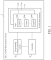
- FIG 1 is a block diagram of a multilevel cell (MLC) NAND flash memory device 1 according to an embodiment of the invention.
- the MLC NAND flash memory device 1 comprises a programming voltage generation circuit 10, a controller 12 and NAND flash memory 14.
- the programming voltage generation circuit 10 is coupled to the NAND flash memory 14, and the pulse to the predetermined page 140.
- the programming voltage generation circuit 10 may apply the initial programming voltage pulse to gate terminals of the selected memory cells of the predetermined page 140 via word lines.
- the initial programming voltage pulse may be a default factory setting conservatively chosen in order to accommodate fast memory cell variations, page-to-page variations and block-to-block variations.
- the controller 12 may verify a plurality of verification levels of the predetermined page 140, and determine a magnitude of a subsequent programming voltage pulse upon one of the plurality of verification levels of the predetermined page 140 passing a verification.
- the determination of the subsequent programming voltage pulse is referred to as a dynamic start voltage (DSV) process.
- the programming voltage generation circuit 10 may further apply the subsequent programming voltage pulse to the predetermined page 140.
- the plurality of verification levels are less than a first-state verification voltage PV(1) of verifying the lowest program state of the predetermined page 140.
- the controller 12 may verify the plurality of verification levels by verifying a verification level of the predetermined page 140 and reducing the verification level to generate a lower verification level when the verification level is verified as failed, and may determine the magnitude of the subsequent programming voltage pulse by determining the magnitude of the subsequent programming voltage pulse according to a difference between the verification level and the first-state verification voltage when the verification level is verified as passed. Further, the controller 12 may reduce the verification level by decrementing the verification level by a fixed amount to generate the lower verification level.
- the first verification level to be verified may be the first-state verification voltage PV(1).
- the first-state verification voltage PV(1) may be -0.8V.
- the fixed amount may be a step voltage equivalent to a step pulse produced by the programming voltage generation circuit 10. For example, the fixed amount may be 0.4V.
- the controller 12 may verify the verification level as passed when one or more of the selected memory cells of the predetermined page 140 are read successfully using the verification level, and verify the verification level as failed when none of the selected memory cells of the predetermined page 140 are read successfully using the verification level.
- the controller 12 may verify the verification level by applying the verification level to the word lines of the selected cells of the predetermined page 140 to read the program states and determine a count of memory cells being read successfully as a fill bit count (FBC).
- FBC fill bit count
- the controller 12 may further verify the first-state verification voltage PV(1), determine the start programming voltage Vpg(1) of the predetermined page 140 according to the initial programming voltage pulse and the subsequent programming voltage pulse when the first-state verification voltage PV(1) is verified as passed, and store the start programming voltage Vpg(1) to the memory location 1400 of the predetermined page 140. More specifically, the start programming voltage Vpg(1) may be determined by summing the initial programming voltage pulse and the subsequent programming voltage pulse. In one embodiment, when it is required to program a memory cell in the predetermined page 140 or another predetermined page 14n to the lowest program state, the controller 12 may read the start programming voltage Vpg(1) from the memory location 1400, and control the programming voltage generation circuit 10 to program the memory cell using the start programming voltage Vpg(1).
- the controller 12 may determine a higher-state programming voltage Vpg(n) according to a verification of a higher-state verification voltage PV(n), and adjust when to verify a higher-state verification voltage PV(n) according to a number of failed verifications of the plurality of verification levels of the predetermined page 140, where n is a positive integer between 2 and 8.
- the higher-state programming voltage Vpg(n) is used to program the selected memory cells into a higher program state n
- the higher-state verification voltage PV(n) is a verification level of verifying the higher program state n.
- determination of the higher-state programming voltage Vpg(n) may be performed using an incremental step pulse programming (ISPP) procedure, in which the selected memory cells in the predetermined page 140 are programmed using a set of fixed-size step pulses generated by the programming voltage generation circuit 10, so as to increment threshold voltages of the selected memory cells in a stepwise manner.
- the controller 12 may regularly verify a corresponding higher-state verification voltage PV(n) as the threshold voltages of the selected memory cells are raised progressively, and identify the higher-state programming voltage Vpg(n) as a summation of all programming pulses upon the corresponding higher-state verification voltage PV(n) being verified as passed.
- the determinations of the higher-state programming voltages Vpg(2) through Vpg(8) may start sequentially after the determination of the start programming voltage Vpg(1), with the higher-state programming voltages Vpg(2) being the first and the higher-state programming voltages Vpg(8) being the last.
- the determination of the higher-state programming voltages Vpg(2) may start at the 5th step pulse of the ISPP procedure, and the determination of the higher-state programming voltages Vpg(3) may start at the 10th step pulse of the ISPP procedure.
- the controller 12 may adjust when to verify a higher-state verification voltage PV(n) by configuring a start step pulse count for starting a verification of the higher-state verification voltage PV(n), and incrementing the start step pulse when the verification level is verified as failed.
- the controller 12 may increment the start step pulse count by a fixed count of the step pulses such as 1 step pulse.
- the controller 12 may start verifying the higher-state verification voltage PV(n); whereas when the accumulated count is less than the start step pulse count, the controller 12 may not verify the higher-state verification voltage PV(n).
- the controller 12 may save an accumulation of step pulses as the higher-state programming voltages Vpg(n) to the memory location 140n. Later, when it is required to program a memory cell into the program state n, the controller 12 may read the higher-state programming voltages Vpg(n) from the memory location 140n, and control the programming voltage generation circuit 10 to program the memory cell using the higher-state programming voltage Vpg(n).
- the MLC NAND flash memory device 1 is not limited to an MLC approach and 8 program states, a single-level cell (SLC) approach or other numbers of program states may be adopted.
- the MLC NAND flash memory device 1 utilizes the multilevel verification to reduce the number of programming voltage pulses to be applied to the predetermined page 140 in order to determine the start programming voltage Vpg(1), thereby speeding up the start programming voltage Vpg(1) determination process considerably for a large start programming voltage shift.
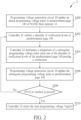
- FIG 2 is a flowchart of a method 2 of determining the start programming voltage Vpg(1) of the MLC NAND flash memory device 1 in FIG. 1 .
- the method 2 comprises Steps S200 through S210. Any reasonable technological change or step adjustment is within the scope of the disclosure.
- Steps S200 through S210 are explained as follows: Step S200: Programming voltage generation circuit 10 applies an initial programming voltage pulse to predetermined page 140 of NAND flash memory 14; Step S202: Controller 12 verifies a plurality of verification levels of predetermined page 140; Step S204: Controller 12 determines a magnitude of a subsequent programming voltage pulse upon one of the plurality of verification levels of the predetermined page 140 passing a verification; Step S206: Programming voltage generation circuit 10 applies the subsequent programming voltage pulse to predetermined page 140; Step S208: Controller 12 determines whether the first-state programming voltage PV(1) is verified as passed? If so, go to Step S210, if not, go to Step S202; Step S210: Controller 12 stores the start programming voltage Vpg(1).
- the programming voltage generation circuit 10 Upon startup, the programming voltage generation circuit 10 applies an initial programming voltage pulse to the predetermined page 140 (S200), the controller 12 employs a multilevel verification by sequentially verifying a plurality of verification levels of predetermined page 140 (S202).
- the plurality of verification levels may start with first-state verification voltage PV(1) and follow by one or more descending verification levels. Eventually, one of the plurality of verification levels may be verified as passed and used to determine the start programming voltage Vpg(1) and a subsequent programming voltage pulse producing the same.
- the controller 12 determines a magnitude of the subsequent programming voltage pulse upon a successful verification of the verification level (S204), the programming voltage generation circuit 10 applies the subsequent programming voltage pulse to predetermined page 140 (S206), and the controller 12 then verifies the first-state programming voltage PV(1) (S208). If the first-state programming voltage PV(1) is verified as passed, a combination of the initial programming voltage pulse and the subsequent programming voltage pulse may be regarded as the start programming voltage Vpg(1), and the controller 12 stores the start programming voltage Vpg(1) into the memory location 1400 (S210). If the first-state programming voltage PV(1) is verified as failed, Steps S202 through S208 are repeated until first-state programming voltage PV(1) is verified as passed. Steps S202 and S204 may be detailed by a method 3 in FIG. 3 , in which determination of the subsequent programming voltage pulse is explained.
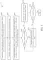
- the method 3 comprises Steps S300 through S306 and is used to verify the plurality of verification levels Vvi, with i being a positive integer. Any reasonable technological change or step adjustment is within the scope of the disclosure. Steps S300 through S306 are explained as follows: Step S300: Controller 12 verifies an initial verification level Vv1; Step S302: Controller 12 determines whether the verification level Vvi is verified as passed?
- Step S304 Controller 12 reduces the verification level Vvi to generate a lower verification level Vvi and verifies the lower verification level Vvi; go to Step S302; Step S306: Controller 12 determines the magnitude of the subsequent programming voltage pulse according to a difference between the verification level Vvi and the first-state verification voltage PV(1).
- the controller 12 Upon startup, the controller 12 verifies an initial verification level Vv1 of the first-state verification voltage PV(1) (S300), and the controller 12 determines whether the verification level Vv1 is verified as passed (S302). If so, the MLC NAND flash memory device 1 may be newly manufactured and the initial programming voltage pulse may be the start programming voltage Vpg(1), the controller 12 determines the magnitude of the subsequent programming voltage pulse according to a difference between the initial verification level Vv1 and the first-state verification voltage PV(1) (S306), and thus no subsequent programming voltage pulse will be applied to the predetermined page 1400 since the initial programming voltage pulse is already the start programming voltage Vpg(1).
- the controller 12 reduces the verification level Vv1 by a decrement to generate a lower verification level Vv2 and verifies the lower verification level Vv2 (S304) and determines whether the verification level Vv2 is verified as passed (S302).
- the decrement may be a fixed amount corresponding to a step pulse produced by the programming voltage generation circuit 10. If the verification level Vv2 is verified as passed, the start programming voltage Vpg(1) may be a combination of the initial programming voltage pulse and the step pulse, the controller 12 determines the magnitude of the subsequent programming voltage pulse according to a difference between the verification level Vv2 and the first-state verification voltage PV(1) (S306).
- the subsequent programming voltage pulse will be one step pulse corresponding to fixed amount of the decrement. If verification level Vv2 is not verified as passed, the controller 12 reduces the verification level Vv2 by another decrement to generate a lower verification level Vv3 (S304). Steps S302 and S304 are repeated continuously until the verification level Vvi is successfully verified and the magnitude of the subsequent programming voltage pulse can be determined.
- FIG. 4 shows a schematic diagram of a start programming voltage determination method 4 employing a 2-level verification according to an embodiment of the invention.
- the start programming voltage determination method 4 comprises Processes 400 through 422, where Processes 400 through 406 are used to perform an initial programming voltage pulse check, Processes 408 through 418 are used to perform the 2-level verification to determine a start programming voltage Vpg(1), and Processes 420 and 422 are used to confirm the start programming voltage Vpg(1).
- the voltage pulse process 400 employs an initial programming voltage pulse and the voltage pulse process 420 employs a subsequent programming voltage pulse.
- the start programming voltage determination method 4 can achieve determination of the start programming voltage Vpg(1) by using only two voltage pulses 400, 420, reducing the time required for determining the start programming voltage Vpg(1).
- FIG. 5 is a flowchart of a method 5 of determining a higher-state programming voltage Vpg(n) of the MLC NAND flash memory device 1 in FIG. 1 .
- the method 5 comprises Steps S500 through S512.
- Steps S500 and S502 are used to perform the multilevel verification, details therefor are provided in Steps S200 and S202 and will not be repeated here for brevity.
- Steps S504 to S512 are used to determine the higher-state programming voltage Vpg(n), where n is a positive integer between 2 and 8. Any reasonable technological change or step adjustment is within the scope of the disclosure.
- Steps S500 through S512 are provided as follows: Step S500: Programming voltage generation circuit applies an initial programming voltage pulse to a predetermined page of NAND flash memory; Step S502: Controller verifies a plurality of verification levels of predetermined page; Step S504: Controller determines when to verify a higher-state verification voltage PV(n) according to the number of failed verifications of the plurality of verification levels of the predetermined page; Step S506: Controller determines whether the higher-state verification voltage PV(n) is verified as passed? If so, go to Step S508, if not, go to Step S512; Step S508: Controller stores the higher-state programming voltage Vpg(n); Step S510: Controller determines whether the highest-state programming voltage PV(8) is verified as passed? If so, exit the method 5, if not, go to Step S512; Step S512: Controller performs an ISPP procedure on the predetermined page; go to Step S506.
- the controller determines when to verify a higher-state verification voltage PV(n) according to the number of failed verifications of the plurality of verification levels of the predetermined page (S504). Specifically, since the higher-state programming voltage Vpg(n) may be shifted by approximately the same amount as the start programming voltage Vpg(1), the controller may skip a verification of the higher-state verification voltage PV(n) and push back the verification by one step pulse when a verification level of the predetermined page is verified as failed. Likewise, the controller may skip a number of verifications of the higher-state verification voltage PV(n) and postpone the verification by the same number of step pulses when the same number of verification levels of the predetermined page are verified as failed in Step S502.
- the controller determines whether the higher-state verification voltage PV(n) is verified as passed (S506), if so, the controller stores an accumulation of step pulses applied to the predetermined page as the higher-state programming voltage Vpg(n) (S508), determine whether the highest-state verification voltage PV(8) is verified as passed (S510), and exit the method 5 when the highest-state verification voltage PV(8) is verified as passed. If the higher-state verification voltage PV(n) is not verified as passed, the controller performs an ISPP procedure on the predetermined page by applying a step pulse to the predetermined page (S512), and Steps S506 through S5are repeated until the highest-state verification voltage PV(8) is verified as passed. If the highest-state verification voltage PV(8) is not verified as passed, the controller continues performing the ISPP procedure on the predetermined page (S512), and Steps S506 through S5are repeated until the highest-state verification voltage PV(8) is verified as passed.
- FIG. 6 shows 4 threshold voltage distributions 60, 62, 64, 66 of memory cells after an initial programming voltage pulse is applied thereto, where the x-axis represents a threshold voltage Vt in volts, and the y-axis represents a quantity in number of memory cells.
- the first-state verification voltage PV(1) is located at -0.8.
- FIG. 6 also shows 4 voltage divisions at -0.8, -1.2, -1.6 and -2.0, separated by a fixed voltage difference corresponding to a step pulse generated by a programming voltage generation circuit.
- Table 1 illustrates the time saved by the present invention in comparison to the ISPP method in the related art, where dVPGM represents 1 step pulse, P represents the time for a programming voltage pulse, V represents the time for a verification, FBC represents the time for a fill bit check, and MLV represents the time for a multi-level verification.
- Each of the threshold voltage distributions 60, 62, 64, 66 contains faster memory cells located at an upper portion of the threshold voltage distribution. Specifically, the faster memory cells of the threshold voltage distributions 60, 62, 64, 66 are located in Ranges C1, C2, C3, C4, respectively.
- the threshold voltages Vt of the faster memory cells of the threshold voltage distributions 60, 62, 64, 66 are respectively 0, 1, 2, 3 voltage differences lower than the first-state verification voltage PV(1), and correspondingly, the start programming voltages Vpg(1) of the threshold voltage distributions 60, 62, 64, 66 are respectively 0, 1, 2, 3 step pulses higher than the initial programming voltage pulse.
- the time saved by the present invention comparing to the ISPP method increases considerably as the threshold voltage distribution is shifted further towards the left. For example, the time saved in the threshold voltage distribution 62 is the time for 6 verifications, and the time saved in the threshold voltage distribution 62 is the time for 2 pulses and 20 verifications.
- the MLC NAND flash memory device 1 and various methods in FIGs. 2 through 5 employ a multilevel verification to accelerate determination of programming voltages.
Landscapes
- Engineering & Computer Science (AREA)
- Computer Hardware Design (AREA)
- Read Only Memory (AREA)
- Microelectronics & Electronic Packaging (AREA)
Claims (13)
- Verfahren zur Programmierung einer NAND-Flash-Speichervorrichtung (1), umfassend:eine Programmierspannungs-Erzeugungseinrichtung (10), die einen initialen Programmierspannungsimpuls an eine vorgegebene Page des NAND-Flash-Speichers (14) anlegt;eine Steuerung (12), die eine Mehrzahl an Verifizierungsstufen der vorgegebenen Page (140) verifiziert, wobei die Mehrzahl an Verifizierungsstufen kleiner ist als eine Erststatus-Verifizierungsspannung zur Verifizierung eines niedrigsten Programmstatus der vorgegebenen Page (140);wobei der Controller (12) eine Größe eines anschließenden Programmierspannungsimpulses bestimmt, nachdem die Verifizierung einer der Mehrzahl an Verifizierungsstufen der vorgegebenen Page (140) erfolgreich war; undwobei die Programmierspannungs-Erzeugungseinrichtung (10) den anschließenden Programmierspannungsimpuls an die vorgegebene Page (140) oder an andere Pagen in dem NAND-Flash-Speicher (14) anlegt, wobei das Verfahren ferner umfasst:dass der Controller (12) entsprechend einer Anzahl von fehlgeschlagenen Verifizierungen der Mehrzahl an Verifizierungsstufen der vorgegebenen Page (140) einstellt, wann eine Verifizierungsspannung eines höheren Status (Vpg(n)) zu verifizieren ist, wobei vorzugsweise
die Einstellung, wann die Verifizierungsspannung des höheren Status zu verifizieren ist, durch den Controller (12) umfasst:dass der Controller (12) eine Startschritt-Impulszahl zum Starten einer Verifizierung der Verifizierungsspannung des höheren Status (Vpg(n)) konfiguriert; unddass der Controller (12) die Startschritt-Impulszahl inkrementiert, wenn die Verifizierungsstufe als fehlgeschlagen verifiziert wird. - Verfahren nach Anspruch 1, wobei die Verifizierung der der Mehrzahl an Verifizierungsstufen der vorgegebenen Page (140) durch den Controller (12v) umfasst:Verifizieren einer Verifizierungsstufe der Mehrzahl an Verifizierungsstufen durch den Controller (12); undReduzieren der Verifizierungsstufe, um eine niedrigere Verifizierungsstufe der Mehrzahl an Verifizierungsstufen zu erzeugen, durch den Controller (12), wenn die Verifizierungsstufe als fehlgeschlagen verifiziert wird, wobei vorzugsweise
die Reduzierung der ersten Verifizierungsstufe durch den Controller (12) umfasst:
Vermindern der ersten Verifizierungsstufe um einen festen Betrag durch den Controller (12), um die niedrigere Verifizierungsstufe zu erzeugen, wenn die Verifizierungsstufe als fehlgeschlagen verifiziert wird. - Verfahren nach Anspruch 1 oder 2, wobei:
die Verifizierung der Mehrzahl an Verifizierungsstufen der vorgegebenen Page (140) durch den Controller (12) umfasst:
Verifizieren einer Verifizierungsstufe der vorgegebenen Page (140) durch den Controller (12); und wobei das Bestimmen der Größe des anschließenden Programmierspannungsimpulses durch den Controller (12) umfasst:
Bestimmen der Größe des anschließenden Programmierspannungsimpulses entsprechend einer Differenz zwischen der Verifizierungsstufe und der Erststatus-Verifizierungsspannung durch den Controller (12), wenn die Verifizierung der Verifizierungsstufe erfolgreich ist, wobei vorzugsweise
die Verifizierungsstufe als erfolgreich verifiziert wird, wenn eine oder mehrere Speicherzellen der vorgegebenen Page mit der Verifizierungsstufe erfolgreich gelesen werden. - Verfahren nach einem der Ansprüche 1 bis 3, ferner umfassend:Verifizieren der Erststatus-Verifizierungsspannung durch den Controller (12);wenn die Erststatus-Verifizierungsspannung als erfolgreich verifiziert wird,
Bestimmen einer Startprogrammierspannung zur Programmierung des niedrigsten Programmstatus der vorgegebenen Page entsprechend dem initialen Programmierspannungsimpuls und dem anschließenden Programmierspannungsimpuls durch den Controller (12); und wobeidas Speichern der Startprogrammierspannung in der vorgegebenen Page vorzugsweise umfasst:
die Programmierung des niedrigsten Programmstatus für die vorgegebene Page oder eine weitere vorgegebene Page des NAND-Flash-Speichers (14) unter Anwendung der Startprogrammierspannung durch die Programmierspannungs-Erzeugungsschaltung. - Verfahren nach einem der Ansprüche 1 bis 4, wobei die vorgegebene Page eine Mehrzahl an Speicherzellen umfasst, die in einem Array angeordnet sind, und wobei jede Speicherzelle in einem von 8 möglichen Programmstatus programmiert werden kann.
- NAND-Flash-Speichervorrichtung (1), umfassend:den NAND-Flash-Speicher (14) mit einer vorgegebenen Page (140) und weiteren Pages;eine Programmierspannungs-Erzeugungseinrichtung (10), die mit dem NAND-Flash-Speicher (14) verbunden ist und eingerichtet ist zum Anlegen eines initialen Programmierspannungsimpulses an die vorgegebene Page (140); undeinen Controller (12), der mit dem NAND-Flash-Speicher (14) und der Programmierspannungs-Erzeugungseinrichtung (10) verbunden ist und eingerichtet ist zum Verifizieren einer Mehrzahl an Verifizierungsstufen der vorgegebenen Page und zum Bestimmen einer Größe eines anschließenden Programmierspannungsimpulses bei erfolgreicher Verifizierung einer der Mehrzahl an Verifizierungsstufen der vorgegebenen Page, wobei die Mehrzahl an Verifizierungsstufen kleiner ist als eine Erststatus-Verifizierungsstufe zur Verifizierung eines niedrigsten Programmstatus der vorgegebenen Page;wobei die Programmierspannungs-Erzeugungseinrichtung (10) ferner eingerichtet ist zum Anlegen des anschließenden Programmierspannungsimpulses an die vorgegebene Page oder weitere Pages in dem NAND-Flash-Speicher,wobei der Controller (12) ferner dazu eingerichtet ist, entsprechend einer Anzahl von fehlgeschlagenen Verifizierungen der Mehrzahl an Verifizierungsstufen der vorgegebenen Page einzustellen, wann eine Verifizierungsspannung eines höheren Status zu verifizieren ist, wobei vorzugsweise der Controller (12) ferner dazu eingerichtet ist einzustellen, wann die Verifizierungsspannung des höheren Status zu verifizieren ist, indem er: eine Startschritt-Impulszahl zum Starten einer Verifizierung der Verifizierungsspannung des höheren Status konfiguriert; und die Startschritt-Impulszahl inkrementiert, wenn die Verifizierungsstufe als fehlgeschlagen verifiziert wird.
- NAND-Flash-Speichervorrichtung (1) nach Anspruch 6, wobei der Controller (12) dazu eingerichtet ist, die Mehrzahl an Verifizierungsstufen der vorgegebenen Page (140) zu verifizieren, indem er eine Verifizierungsstufe der vorgegebenen Page (140) verifiziert, und die Verifizierungsstufe zu reduzieren, um eine niedrigere Verifizierungsstufe der Mehrzahl an Verifizierungsstufen zu erzeugen, wenn die Verifizierungsstufe als fehlgeschlagen verifiziert wird.
- NAND-Flash-Speichervorrichtung (1) nach Anspruch 7, wobei der Controller (12) dazu eingerichtet ist, die Verifizierungsstufe der vorgegebenen Page zu reduzieren, indem er die Verifizierungsstufe der vorgegebenen Page um einen festen Betrag vermindert, um die niedrigere Verifizierungsstufe zu erzeugen, wenn die Verifizierungsstufe als fehlgeschlagen verifiziert wird.
- NAND-Flash-Speichervorrichtung (1) nach einem der Ansprüche 6 bis 8, wobei der Controller (12) eingerichtet ist zum Verifizieren der Mehrzahl an Verifizierungsstufen der vorgegebenen Page (140) durch Verifizieren einer Verifizierungsstufe der vorgegebenen Page (140) und zum Bestimmen der Größe des anschließenden Programmierspannungsimpulses durch Bestimmen der Größe des anschließenden Programmierspannungsimpulses entsprechend einer Differenz zwischen der Verifizierungsstufe und der Erststatus-Verifizierungsspannung, wenn die Verifizierungsstufe als erfolgreich verifiziert wird.
- NAND-Flash-Speichervorrichtung (1) nach Anspruch 9, wobei der Controller (12) eingerichtet ist zum Verifizieren der Verifizierungsstufe als erfolgreich, wenn eine oder mehrere Speicherzellen der vorgegebenen Page mit der Verifizierungsstufe erfolgreich gelesen werden.
- NAND-Flash-Speichervorrichtung (1) nach einem der Ansprüche 6 bis 10, wobei der Controller (12) ferner eingerichtet ist zum Verifizieren der Erststatus-Verifizierungsspannung, wenn die Erststatus-Verifizierungsspannung als erfolgreich verifiziert wird, zum Bestimmen einer Startprogrammierspannung zur Programmierung des niedrigsten Programmstatus der vorgegebenen Page entsprechend dem initialen Programmierspannungsimpuls und dem anschließenden Programmierspannungsimpuls und zum Speichern der Startprogrammierspannung in der vorgegebenen Page.
- NAND-Flash-Speichervorrichtung (1) nach Anspruch 11, wobei die Programmierspannungs-Erzeugungsschaltung (10) ferner eingerichtet ist zum Programmieren des niedrigsten Programmstatus für die vorgegebenen Page oder eine andere vorgegebenen Page des NAND-Flash-Speichers (14) mit Hilfe der Startprogrammierspannung.
- NAND-Flash-Speichervorrichtung (1) nach einem der Ansprüche 6 bis 12, wobei die vorgegebenen Page eine Mehrzahl an Speicherzellen umfasst, die in einem Array angeordnet sind, und wobei jede Speicherzelle in 8 möglichen Programmstatus programmiert werden kann.
Priority Applications (1)
| Application Number | Priority Date | Filing Date | Title |
|---|---|---|---|
| EP24216114.9A EP4510134A3 (de) | 2019-05-22 | 2019-05-22 | Verfahren zur programmierung einer mehrstufigen zellen-nand-flash-speichervorrichtung und mlc-nand-flash-speichervorrichtung |
Applications Claiming Priority (1)
| Application Number | Priority Date | Filing Date | Title |
|---|---|---|---|
| PCT/CN2019/087903 WO2020232658A1 (en) | 2019-05-22 | 2019-05-22 | Method of programming multilevel cell nand flash memory device and mlc nand flash memory device |
Related Child Applications (2)
| Application Number | Title | Priority Date | Filing Date |
|---|---|---|---|
| EP24216114.9A Division-Into EP4510134A3 (de) | 2019-05-22 | 2019-05-22 | Verfahren zur programmierung einer mehrstufigen zellen-nand-flash-speichervorrichtung und mlc-nand-flash-speichervorrichtung |
| EP24216114.9A Division EP4510134A3 (de) | 2019-05-22 | 2019-05-22 | Verfahren zur programmierung einer mehrstufigen zellen-nand-flash-speichervorrichtung und mlc-nand-flash-speichervorrichtung |
Publications (3)
| Publication Number | Publication Date |
|---|---|
| EP3909050A1 EP3909050A1 (de) | 2021-11-17 |
| EP3909050A4 EP3909050A4 (de) | 2022-08-24 |
| EP3909050B1 true EP3909050B1 (de) | 2025-01-01 |
Family
ID=68150187
Family Applications (2)
| Application Number | Title | Priority Date | Filing Date |
|---|---|---|---|
| EP19929556.9A Active EP3909050B1 (de) | 2019-05-22 | 2019-05-22 | Verfahren zur programmierung einer mehrstufigen nand-flash-speichervorrichtung und mlc-nand-flash-speichervorrichtung |
| EP24216114.9A Pending EP4510134A3 (de) | 2019-05-22 | 2019-05-22 | Verfahren zur programmierung einer mehrstufigen zellen-nand-flash-speichervorrichtung und mlc-nand-flash-speichervorrichtung |
Family Applications After (1)
| Application Number | Title | Priority Date | Filing Date |
|---|---|---|---|
| EP24216114.9A Pending EP4510134A3 (de) | 2019-05-22 | 2019-05-22 | Verfahren zur programmierung einer mehrstufigen zellen-nand-flash-speichervorrichtung und mlc-nand-flash-speichervorrichtung |
Country Status (7)
| Country | Link |
|---|---|
| US (1) | US10937514B2 (de) |
| EP (2) | EP3909050B1 (de) |
| JP (1) | JP7295267B2 (de) |
| KR (1) | KR102871781B1 (de) |
| CN (2) | CN112530497B (de) |
| TW (1) | TWI717781B (de) |
| WO (1) | WO2020232658A1 (de) |
Families Citing this family (4)
| Publication number | Priority date | Publication date | Assignee | Title |
|---|---|---|---|---|
| CN112967746B (zh) * | 2020-08-13 | 2022-09-16 | 长江存储科技有限责任公司 | 用于对存储器系统进行编程的方法、装置及存储器系统 |
| US11361834B1 (en) * | 2020-12-30 | 2022-06-14 | Sandisk Technologies Llc | Systems and methods for dual-pulse programming |
| CN112634968A (zh) * | 2021-01-08 | 2021-04-09 | 长江存储科技有限责任公司 | 编程脉冲的方法、装置、计算机可读存储介质和处理器 |
| CN112802507B (zh) * | 2021-01-25 | 2022-11-29 | 长江存储科技有限责任公司 | 三维存储器及其控制方法 |
Family Cites Families (25)
| Publication number | Priority date | Publication date | Assignee | Title |
|---|---|---|---|---|
| JP2002319286A (ja) * | 2001-04-19 | 2002-10-31 | Hitachi Ltd | 不揮発性記憶装置および記憶システム |
| JP4086583B2 (ja) * | 2002-08-08 | 2008-05-14 | シャープ株式会社 | 不揮発性半導体メモリ装置およびデータ書き込み制御方法 |
| US7453731B2 (en) * | 2006-09-12 | 2008-11-18 | Sandisk Corporation | Method for non-volatile memory with linear estimation of initial programming voltage |
| KR100780773B1 (ko) * | 2006-11-03 | 2007-11-30 | 주식회사 하이닉스반도체 | 플래시 메모리소자의 프로그램 시작 바이어스 설정방법 및이를 이용한 프로그램 방법 |
| KR20080060799A (ko) * | 2006-12-27 | 2008-07-02 | 삼성전자주식회사 | 테스트 시간을 감소할 수 있는 멀티 레벨 셀 낸드 플래시메모리 장치 및 그것의 테스트 방법 |
| US8085591B2 (en) * | 2008-05-20 | 2011-12-27 | Micron Technology, Inc. | Charge loss compensation during programming of a memory device |
| KR100953045B1 (ko) * | 2008-05-23 | 2010-04-14 | 주식회사 하이닉스반도체 | 불휘발성 메모리 장치의 프로그램 방법 |
| KR100965071B1 (ko) * | 2008-07-10 | 2010-06-21 | 주식회사 하이닉스반도체 | 불휘발성 메모리 장치의 프로그램 방법 |
| US8854887B2 (en) * | 2008-07-10 | 2014-10-07 | Hynix Semiconductor Inc. | Nonvolatile memory device and method of programming the same |
| US8045375B2 (en) * | 2008-10-24 | 2011-10-25 | Sandisk Technologies Inc. | Programming non-volatile memory with high resolution variable initial programming pulse |
| KR100996108B1 (ko) * | 2009-01-21 | 2010-11-22 | 주식회사 하이닉스반도체 | 불휘발성 메모리 장치의 프로그램 방법 |
| KR101074539B1 (ko) * | 2009-02-04 | 2011-10-17 | 주식회사 하이닉스반도체 | 불휘발성 메모리 장치 및 그 동작 방법 |
| US8223555B2 (en) | 2009-05-07 | 2012-07-17 | Micron Technology, Inc. | Multiple level program verify in a memory device |
| JP2011258260A (ja) * | 2010-06-07 | 2011-12-22 | Toshiba Corp | 不揮発性半導体記憶装置 |
| KR102016041B1 (ko) * | 2012-10-11 | 2019-08-30 | 삼성전자주식회사 | 비휘발성 메모리 장치의 프로그램 방법 |
| KR20150061098A (ko) * | 2013-11-25 | 2015-06-04 | 삼성전자주식회사 | 메모리 시스템 및 상기 메모리 시스템의 프로그래밍 방법 |
| KR20150094129A (ko) * | 2014-02-10 | 2015-08-19 | 에스케이하이닉스 주식회사 | 반도체 장치 및 이의 동작 방법 |
| US9171628B2 (en) * | 2014-03-13 | 2015-10-27 | Macronix International Co., Ltd. | Incremental step pulse programming (ISPP) scheme capable of determining a next starting pulse based on a current program-verify pulse for improving programming speed |
| US9576673B2 (en) * | 2014-10-07 | 2017-02-21 | Sandisk Technologies Llc | Sensing multiple reference levels in non-volatile storage elements |
| US20160300620A1 (en) * | 2015-04-08 | 2016-10-13 | Sandisk Technologies Inc. | Multiple bit line voltage sensing for non-volatile memory |
| TWI550616B (zh) * | 2015-07-03 | 2016-09-21 | 力晶科技股份有限公司 | 快閃記憶體裝置及其程式化動作的初始化方法 |
| US9792999B2 (en) * | 2015-10-30 | 2017-10-17 | SK Hynix Inc. | Adaptive scheme for incremental step pulse programming of flash memory |
| KR102458918B1 (ko) * | 2016-02-24 | 2022-10-25 | 삼성전자주식회사 | 메모리 장치 및 메모리 시스템 |
| TWI604449B (zh) * | 2016-08-31 | 2017-11-01 | 旺宏電子股份有限公司 | 記憶體裝置與其程式化方法 |
| CN109408402B (zh) * | 2018-10-09 | 2021-06-01 | 长江存储科技有限责任公司 | 一种闪存器的数据写入方法及闪存器 |
-
2019
- 2019-05-22 WO PCT/CN2019/087903 patent/WO2020232658A1/en not_active Ceased
- 2019-05-22 KR KR1020217027688A patent/KR102871781B1/ko active Active
- 2019-05-22 EP EP19929556.9A patent/EP3909050B1/de active Active
- 2019-05-22 JP JP2021559122A patent/JP7295267B2/ja active Active
- 2019-05-22 EP EP24216114.9A patent/EP4510134A3/de active Pending
- 2019-05-22 CN CN202011408342.9A patent/CN112530497B/zh active Active
- 2019-05-22 CN CN201980000912.XA patent/CN110337694B/zh active Active
- 2019-07-15 TW TW108124900A patent/TWI717781B/zh active
- 2019-07-16 US US16/513,658 patent/US10937514B2/en active Active
Also Published As
| Publication number | Publication date |
|---|---|
| EP3909050A4 (de) | 2022-08-24 |
| JP2022528898A (ja) | 2022-06-16 |
| JP7295267B2 (ja) | 2023-06-20 |
| US10937514B2 (en) | 2021-03-02 |
| EP4510134A3 (de) | 2025-05-07 |
| EP4510134A2 (de) | 2025-02-19 |
| TW202044253A (zh) | 2020-12-01 |
| CN110337694B (zh) | 2020-12-18 |
| US20200372963A1 (en) | 2020-11-26 |
| CN110337694A (zh) | 2019-10-15 |
| CN112530497B (zh) | 2022-08-12 |
| WO2020232658A1 (en) | 2020-11-26 |
| KR102871781B1 (ko) | 2025-10-15 |
| TWI717781B (zh) | 2021-02-01 |
| KR20210118462A (ko) | 2021-09-30 |
| EP3909050A1 (de) | 2021-11-17 |
| CN112530497A (zh) | 2021-03-19 |
Similar Documents
| Publication | Publication Date | Title |
|---|---|---|
| US7558115B2 (en) | Program method of flash memory device | |
| EP3909050B1 (de) | Verfahren zur programmierung einer mehrstufigen nand-flash-speichervorrichtung und mlc-nand-flash-speichervorrichtung | |
| US7116581B2 (en) | Nonvolatile semiconductor memory device and method of programming in nonvolatile semiconductor memory device | |
| US7151692B2 (en) | Operation scheme for programming charge trapping non-volatile memory | |
| EP3891748B1 (de) | Verfahren zur programmierung einer nichtflüchtigen speichervorrichtung durch anlegen mehrerer bitleitungsvorspannungen | |
| USRE45544E1 (en) | Saw-shaped multi-pulse programming for program noise reduction in memory | |
| US8174894B2 (en) | Program method of flash memory device | |
| US10699776B1 (en) | Apparatus and methods for merging post-write read and select gate maintenance operations | |
| US11264091B1 (en) | Operating method of generating enhanced bit line voltage and non-volatile memory device | |
| US11145362B2 (en) | Method for programming memory system | |
| US8085597B2 (en) | Nonvolatile semiconductor memory and data writing method for nonvolatile semiconductor memory | |
| KR100818717B1 (ko) | 비휘발성 반도체 메모리 장치 및 상기 비휘발성 반도체메모리 장치의 프로그램 방법 | |
| US10811111B1 (en) | Non-volatile memory device and method for programming in non-volatile memory device by applying multiple bitline bias voltages | |
| US8391069B2 (en) | Programming method for nonvolatile semiconductor memory device | |
| KR101604857B1 (ko) | 반도체 메모리 장치의 프로그램 방법 |
Legal Events
| Date | Code | Title | Description |
|---|---|---|---|
| STAA | Information on the status of an ep patent application or granted ep patent |
Free format text: STATUS: THE INTERNATIONAL PUBLICATION HAS BEEN MADE |
|
| PUAI | Public reference made under article 153(3) epc to a published international application that has entered the european phase |
Free format text: ORIGINAL CODE: 0009012 |
|
| STAA | Information on the status of an ep patent application or granted ep patent |
Free format text: STATUS: REQUEST FOR EXAMINATION WAS MADE |
|
| 17P | Request for examination filed |
Effective date: 20210812 |
|
| AK | Designated contracting states |
Kind code of ref document: A1 Designated state(s): AL AT BE BG CH CY CZ DE DK EE ES FI FR GB GR HR HU IE IS IT LI LT LU LV MC MK MT NL NO PL PT RO RS SE SI SK SM TR |
|
| A4 | Supplementary search report drawn up and despatched |
Effective date: 20220727 |
|
| RIC1 | Information provided on ipc code assigned before grant |
Ipc: G11C 16/34 20060101ALI20220722BHEP Ipc: G11C 16/12 20060101AFI20220722BHEP |
|
| DAV | Request for validation of the european patent (deleted) | ||
| DAX | Request for extension of the european patent (deleted) | ||
| STAA | Information on the status of an ep patent application or granted ep patent |
Free format text: STATUS: EXAMINATION IS IN PROGRESS |
|
| 17Q | First examination report despatched |
Effective date: 20231106 |
|
| GRAP | Despatch of communication of intention to grant a patent |
Free format text: ORIGINAL CODE: EPIDOSNIGR1 |
|
| STAA | Information on the status of an ep patent application or granted ep patent |
Free format text: STATUS: GRANT OF PATENT IS INTENDED |
|
| INTG | Intention to grant announced |
Effective date: 20240726 |
|
| GRAS | Grant fee paid |
Free format text: ORIGINAL CODE: EPIDOSNIGR3 |
|
| GRAA | (expected) grant |
Free format text: ORIGINAL CODE: 0009210 |
|
| STAA | Information on the status of an ep patent application or granted ep patent |
Free format text: STATUS: THE PATENT HAS BEEN GRANTED |
|
| P01 | Opt-out of the competence of the unified patent court (upc) registered |
Free format text: CASE NUMBER: APP_61765/2024 Effective date: 20241119 |
|
| AK | Designated contracting states |
Kind code of ref document: B1 Designated state(s): AL AT BE BG CH CY CZ DE DK EE ES FI FR GB GR HR HU IE IS IT LI LT LU LV MC MK MT NL NO PL PT RO RS SE SI SK SM TR |
|
| RAP3 | Party data changed (applicant data changed or rights of an application transferred) |
Owner name: YANGTZE MEMORY TECHNOLOGIES CO., LTD. |
|
| REG | Reference to a national code |
Ref country code: GB Ref legal event code: FG4D |
|
| RIN1 | Information on inventor provided before grant (corrected) |
Inventor name: WAN, WEI JUN |
|
| REG | Reference to a national code |
Ref country code: CH Ref legal event code: EP |
|
| REG | Reference to a national code |
Ref country code: DE Ref legal event code: R096 Ref document number: 602019064477 Country of ref document: DE |
|
| REG | Reference to a national code |
Ref country code: IE Ref legal event code: FG4D |
|
| REG | Reference to a national code |
Ref country code: LT Ref legal event code: MG9D |
|
| REG | Reference to a national code |
Ref country code: NL Ref legal event code: MP Effective date: 20250101 |
|
| REG | Reference to a national code |
Ref country code: AT Ref legal event code: MK05 Ref document number: 1757150 Country of ref document: AT Kind code of ref document: T Effective date: 20250101 |
|
| PG25 | Lapsed in a contracting state [announced via postgrant information from national office to epo] |
Ref country code: NL Free format text: LAPSE BECAUSE OF FAILURE TO SUBMIT A TRANSLATION OF THE DESCRIPTION OR TO PAY THE FEE WITHIN THE PRESCRIBED TIME-LIMIT Effective date: 20250101 |
|
| PG25 | Lapsed in a contracting state [announced via postgrant information from national office to epo] |
Ref country code: FI Free format text: LAPSE BECAUSE OF FAILURE TO SUBMIT A TRANSLATION OF THE DESCRIPTION OR TO PAY THE FEE WITHIN THE PRESCRIBED TIME-LIMIT Effective date: 20250101 |
|
| PG25 | Lapsed in a contracting state [announced via postgrant information from national office to epo] |
Ref country code: PL Free format text: LAPSE BECAUSE OF FAILURE TO SUBMIT A TRANSLATION OF THE DESCRIPTION OR TO PAY THE FEE WITHIN THE PRESCRIBED TIME-LIMIT Effective date: 20250101 |
|
| PGFP | Annual fee paid to national office [announced via postgrant information from national office to epo] |
Ref country code: DE Payment date: 20250522 Year of fee payment: 7 |
|
| PG25 | Lapsed in a contracting state [announced via postgrant information from national office to epo] |
Ref country code: ES Free format text: LAPSE BECAUSE OF FAILURE TO SUBMIT A TRANSLATION OF THE DESCRIPTION OR TO PAY THE FEE WITHIN THE PRESCRIBED TIME-LIMIT Effective date: 20250101 |
|
| PG25 | Lapsed in a contracting state [announced via postgrant information from national office to epo] |
Ref country code: NO Free format text: LAPSE BECAUSE OF FAILURE TO SUBMIT A TRANSLATION OF THE DESCRIPTION OR TO PAY THE FEE WITHIN THE PRESCRIBED TIME-LIMIT Effective date: 20250401 Ref country code: IS Free format text: LAPSE BECAUSE OF FAILURE TO SUBMIT A TRANSLATION OF THE DESCRIPTION OR TO PAY THE FEE WITHIN THE PRESCRIBED TIME-LIMIT Effective date: 20250501 |
|
| PG25 | Lapsed in a contracting state [announced via postgrant information from national office to epo] |
Ref country code: HR Free format text: LAPSE BECAUSE OF FAILURE TO SUBMIT A TRANSLATION OF THE DESCRIPTION OR TO PAY THE FEE WITHIN THE PRESCRIBED TIME-LIMIT Effective date: 20250101 |
|
| PG25 | Lapsed in a contracting state [announced via postgrant information from national office to epo] |
Ref country code: LV Free format text: LAPSE BECAUSE OF FAILURE TO SUBMIT A TRANSLATION OF THE DESCRIPTION OR TO PAY THE FEE WITHIN THE PRESCRIBED TIME-LIMIT Effective date: 20250101 Ref country code: PT Free format text: LAPSE BECAUSE OF FAILURE TO SUBMIT A TRANSLATION OF THE DESCRIPTION OR TO PAY THE FEE WITHIN THE PRESCRIBED TIME-LIMIT Effective date: 20250502 |
|
| PG25 | Lapsed in a contracting state [announced via postgrant information from national office to epo] |
Ref country code: GR Free format text: LAPSE BECAUSE OF FAILURE TO SUBMIT A TRANSLATION OF THE DESCRIPTION OR TO PAY THE FEE WITHIN THE PRESCRIBED TIME-LIMIT Effective date: 20250402 Ref country code: BG Free format text: LAPSE BECAUSE OF FAILURE TO SUBMIT A TRANSLATION OF THE DESCRIPTION OR TO PAY THE FEE WITHIN THE PRESCRIBED TIME-LIMIT Effective date: 20250101 |
|
| PG25 | Lapsed in a contracting state [announced via postgrant information from national office to epo] |
Ref country code: AT Free format text: LAPSE BECAUSE OF FAILURE TO SUBMIT A TRANSLATION OF THE DESCRIPTION OR TO PAY THE FEE WITHIN THE PRESCRIBED TIME-LIMIT Effective date: 20250101 |
|
| PG25 | Lapsed in a contracting state [announced via postgrant information from national office to epo] |
Ref country code: CZ Free format text: LAPSE BECAUSE OF FAILURE TO SUBMIT A TRANSLATION OF THE DESCRIPTION OR TO PAY THE FEE WITHIN THE PRESCRIBED TIME-LIMIT Effective date: 20250101 |
|
| PG25 | Lapsed in a contracting state [announced via postgrant information from national office to epo] |
Ref country code: SE Free format text: LAPSE BECAUSE OF FAILURE TO SUBMIT A TRANSLATION OF THE DESCRIPTION OR TO PAY THE FEE WITHIN THE PRESCRIBED TIME-LIMIT Effective date: 20250101 |
|
| REG | Reference to a national code |
Ref country code: DE Ref legal event code: R097 Ref document number: 602019064477 Country of ref document: DE |
|
| PG25 | Lapsed in a contracting state [announced via postgrant information from national office to epo] |
Ref country code: SM Free format text: LAPSE BECAUSE OF FAILURE TO SUBMIT A TRANSLATION OF THE DESCRIPTION OR TO PAY THE FEE WITHIN THE PRESCRIBED TIME-LIMIT Effective date: 20250101 |
|
| PG25 | Lapsed in a contracting state [announced via postgrant information from national office to epo] |
Ref country code: DK Free format text: LAPSE BECAUSE OF FAILURE TO SUBMIT A TRANSLATION OF THE DESCRIPTION OR TO PAY THE FEE WITHIN THE PRESCRIBED TIME-LIMIT Effective date: 20250101 |
|
| PG25 | Lapsed in a contracting state [announced via postgrant information from national office to epo] |
Ref country code: IT Free format text: LAPSE BECAUSE OF FAILURE TO SUBMIT A TRANSLATION OF THE DESCRIPTION OR TO PAY THE FEE WITHIN THE PRESCRIBED TIME-LIMIT Effective date: 20250101 |
|
| PG25 | Lapsed in a contracting state [announced via postgrant information from national office to epo] |
Ref country code: EE Free format text: LAPSE BECAUSE OF FAILURE TO SUBMIT A TRANSLATION OF THE DESCRIPTION OR TO PAY THE FEE WITHIN THE PRESCRIBED TIME-LIMIT Effective date: 20250101 |
|
| PG25 | Lapsed in a contracting state [announced via postgrant information from national office to epo] |
Ref country code: RO Free format text: LAPSE BECAUSE OF FAILURE TO SUBMIT A TRANSLATION OF THE DESCRIPTION OR TO PAY THE FEE WITHIN THE PRESCRIBED TIME-LIMIT Effective date: 20250101 |
|
| PG25 | Lapsed in a contracting state [announced via postgrant information from national office to epo] |
Ref country code: SK Free format text: LAPSE BECAUSE OF FAILURE TO SUBMIT A TRANSLATION OF THE DESCRIPTION OR TO PAY THE FEE WITHIN THE PRESCRIBED TIME-LIMIT Effective date: 20250101 |
|
| PLBE | No opposition filed within time limit |
Free format text: ORIGINAL CODE: 0009261 |
|
| STAA | Information on the status of an ep patent application or granted ep patent |
Free format text: STATUS: NO OPPOSITION FILED WITHIN TIME LIMIT |
|
| REG | Reference to a national code |
Ref country code: CH Ref legal event code: L10 Free format text: ST27 STATUS EVENT CODE: U-0-0-L10-L00 (AS PROVIDED BY THE NATIONAL OFFICE) Effective date: 20251112 |
|
| 26N | No opposition filed |
Effective date: 20251002 |
|
| REG | Reference to a national code |
Ref country code: CH Ref legal event code: H13 Free format text: ST27 STATUS EVENT CODE: U-0-0-H10-H13 (AS PROVIDED BY THE NATIONAL OFFICE) Effective date: 20251223 |
|
| PG25 | Lapsed in a contracting state [announced via postgrant information from national office to epo] |
Ref country code: LU Free format text: LAPSE BECAUSE OF NON-PAYMENT OF DUE FEES Effective date: 20250522 |
|
| PG25 | Lapsed in a contracting state [announced via postgrant information from national office to epo] |
Ref country code: CH Free format text: LAPSE BECAUSE OF NON-PAYMENT OF DUE FEES Effective date: 20250531 |
|
| REG | Reference to a national code |
Ref country code: BE Ref legal event code: MM Effective date: 20250531 |
|
| PG25 | Lapsed in a contracting state [announced via postgrant information from national office to epo] |
Ref country code: MC Free format text: LAPSE BECAUSE OF FAILURE TO SUBMIT A TRANSLATION OF THE DESCRIPTION OR TO PAY THE FEE WITHIN THE PRESCRIBED TIME-LIMIT Effective date: 20250101 |
|
| PGFP | Annual fee paid to national office [announced via postgrant information from national office to epo] |
Ref country code: GB Payment date: 20260323 Year of fee payment: 8 |
|
| PG25 | Lapsed in a contracting state [announced via postgrant information from national office to epo] |
Ref country code: IE Free format text: LAPSE BECAUSE OF NON-PAYMENT OF DUE FEES Effective date: 20250522 |
|
| PG25 | Lapsed in a contracting state [announced via postgrant information from national office to epo] |
Ref country code: BE Free format text: LAPSE BECAUSE OF NON-PAYMENT OF DUE FEES Effective date: 20250531 |
|
| PGFP | Annual fee paid to national office [announced via postgrant information from national office to epo] |
Ref country code: FR Payment date: 20260317 Year of fee payment: 8 |