EP3885802B1 - Optischer körper und anzeigevorrichtung damit - Google Patents
Optischer körper und anzeigevorrichtung damit Download PDFInfo
- Publication number
- EP3885802B1 EP3885802B1 EP19886144.5A EP19886144A EP3885802B1 EP 3885802 B1 EP3885802 B1 EP 3885802B1 EP 19886144 A EP19886144 A EP 19886144A EP 3885802 B1 EP3885802 B1 EP 3885802B1
- Authority
- EP
- European Patent Office
- Prior art keywords
- dispersion
- optical body
- dispersions
- cross
- substrate
- Prior art date
- Legal status (The legal status is an assumption and is not a legal conclusion. Google has not performed a legal analysis and makes no representation as to the accuracy of the status listed.)
- Active
Links
Images


Classifications
-
- G—PHYSICS
- G02—OPTICS
- G02B—OPTICAL ELEMENTS, SYSTEMS OR APPARATUS
- G02B5/00—Optical elements other than lenses
- G02B5/30—Polarising elements
- G02B5/3008—Polarising elements comprising dielectric particles, e.g. birefringent crystals embedded in a matrix
-
- G—PHYSICS
- G02—OPTICS
- G02F—OPTICAL DEVICES OR ARRANGEMENTS FOR THE CONTROL OF LIGHT BY MODIFICATION OF THE OPTICAL PROPERTIES OF THE MEDIA OF THE ELEMENTS INVOLVED THEREIN; NON-LINEAR OPTICS; FREQUENCY-CHANGING OF LIGHT; OPTICAL LOGIC ELEMENTS; OPTICAL ANALOGUE/DIGITAL CONVERTERS
- G02F1/00—Devices or arrangements for the control of the intensity, colour, phase, polarisation or direction of light arriving from an independent light source, e.g. switching, gating or modulating; Non-linear optics
- G02F1/01—Devices or arrangements for the control of the intensity, colour, phase, polarisation or direction of light arriving from an independent light source, e.g. switching, gating or modulating; Non-linear optics for the control of the intensity, phase, polarisation or colour
- G02F1/13—Devices or arrangements for the control of the intensity, colour, phase, polarisation or direction of light arriving from an independent light source, e.g. switching, gating or modulating; Non-linear optics for the control of the intensity, phase, polarisation or colour based on liquid crystals, e.g. single liquid crystal display cells
- G02F1/133—Constructional arrangements; Operation of liquid crystal cells; Circuit arrangements
- G02F1/1333—Constructional arrangements; Manufacturing methods
- G02F1/1335—Structural association of cells with optical devices, e.g. polarisers or reflectors
- G02F1/133524—Light-guides, e.g. fibre-optic bundles, louvered or jalousie light-guides
-
- G—PHYSICS
- G02—OPTICS
- G02B—OPTICAL ELEMENTS, SYSTEMS OR APPARATUS
- G02B1/00—Optical elements characterised by the material of which they are made; Optical coatings for optical elements
- G02B1/04—Optical elements characterised by the material of which they are made; Optical coatings for optical elements made of organic materials, e.g. plastics
-
- G—PHYSICS
- G02—OPTICS
- G02B—OPTICAL ELEMENTS, SYSTEMS OR APPARATUS
- G02B27/00—Optical systems or apparatus not provided for by any of the groups G02B1/00 - G02B26/00, G02B30/00
- G02B27/28—Optical systems or apparatus not provided for by any of the groups G02B1/00 - G02B26/00, G02B30/00 for polarising
- G02B27/286—Optical systems or apparatus not provided for by any of the groups G02B1/00 - G02B26/00, G02B30/00 for polarising for controlling or changing the state of polarisation, e.g. transforming one polarisation state into another
-
- G—PHYSICS
- G02—OPTICS
- G02B—OPTICAL ELEMENTS, SYSTEMS OR APPARATUS
- G02B6/00—Light guides; Structural details of arrangements comprising light guides and other optical elements, e.g. couplings
- G02B6/0001—Light guides; Structural details of arrangements comprising light guides and other optical elements, e.g. couplings specially adapted for lighting devices or systems
- G02B6/0011—Light guides; Structural details of arrangements comprising light guides and other optical elements, e.g. couplings specially adapted for lighting devices or systems the light guides being planar or of plate-like form
- G02B6/0033—Means for improving the coupling-out of light from the light guide
- G02B6/0035—Means for improving the coupling-out of light from the light guide provided on the surface of the light guide or in the bulk of it
- G02B6/004—Scattering dots or dot-like elements, e.g. microbeads, scattering particles, nanoparticles
- G02B6/0041—Scattering dots or dot-like elements, e.g. microbeads, scattering particles, nanoparticles provided in the bulk of the light guide
-
- G—PHYSICS
- G02—OPTICS
- G02B—OPTICAL ELEMENTS, SYSTEMS OR APPARATUS
- G02B6/00—Light guides; Structural details of arrangements comprising light guides and other optical elements, e.g. couplings
- G02B6/0001—Light guides; Structural details of arrangements comprising light guides and other optical elements, e.g. couplings specially adapted for lighting devices or systems
- G02B6/0011—Light guides; Structural details of arrangements comprising light guides and other optical elements, e.g. couplings specially adapted for lighting devices or systems the light guides being planar or of plate-like form
- G02B6/0033—Means for improving the coupling-out of light from the light guide
- G02B6/0035—Means for improving the coupling-out of light from the light guide provided on the surface of the light guide or in the bulk of it
- G02B6/004—Scattering dots or dot-like elements, e.g. microbeads, scattering particles, nanoparticles
- G02B6/0043—Scattering dots or dot-like elements, e.g. microbeads, scattering particles, nanoparticles provided on the surface of the light guide
-
- G—PHYSICS
- G02—OPTICS
- G02B—OPTICAL ELEMENTS, SYSTEMS OR APPARATUS
- G02B6/00—Light guides; Structural details of arrangements comprising light guides and other optical elements, e.g. couplings
- G02B6/0001—Light guides; Structural details of arrangements comprising light guides and other optical elements, e.g. couplings specially adapted for lighting devices or systems
- G02B6/0011—Light guides; Structural details of arrangements comprising light guides and other optical elements, e.g. couplings specially adapted for lighting devices or systems the light guides being planar or of plate-like form
- G02B6/0033—Means for improving the coupling-out of light from the light guide
- G02B6/005—Means for improving the coupling-out of light from the light guide provided by one optical element, or plurality thereof, placed on the light output side of the light guide
- G02B6/0055—Reflecting element, sheet or layer
-
- G—PHYSICS
- G02—OPTICS
- G02B—OPTICAL ELEMENTS, SYSTEMS OR APPARATUS
- G02B6/00—Light guides; Structural details of arrangements comprising light guides and other optical elements, e.g. couplings
- G02B6/0001—Light guides; Structural details of arrangements comprising light guides and other optical elements, e.g. couplings specially adapted for lighting devices or systems
- G02B6/0011—Light guides; Structural details of arrangements comprising light guides and other optical elements, e.g. couplings specially adapted for lighting devices or systems the light guides being planar or of plate-like form
- G02B6/0033—Means for improving the coupling-out of light from the light guide
- G02B6/0056—Means for improving the coupling-out of light from the light guide for producing polarisation effects, e.g. by a surface with polarizing properties or by an additional polarizing elements
-
- G—PHYSICS
- G02—OPTICS
- G02B—OPTICAL ELEMENTS, SYSTEMS OR APPARATUS
- G02B6/00—Light guides; Structural details of arrangements comprising light guides and other optical elements, e.g. couplings
- G02B6/0001—Light guides; Structural details of arrangements comprising light guides and other optical elements, e.g. couplings specially adapted for lighting devices or systems
- G02B6/0011—Light guides; Structural details of arrangements comprising light guides and other optical elements, e.g. couplings specially adapted for lighting devices or systems the light guides being planar or of plate-like form
- G02B6/0065—Manufacturing aspects; Material aspects
-
- G—PHYSICS
- G02—OPTICS
- G02F—OPTICAL DEVICES OR ARRANGEMENTS FOR THE CONTROL OF LIGHT BY MODIFICATION OF THE OPTICAL PROPERTIES OF THE MEDIA OF THE ELEMENTS INVOLVED THEREIN; NON-LINEAR OPTICS; FREQUENCY-CHANGING OF LIGHT; OPTICAL LOGIC ELEMENTS; OPTICAL ANALOGUE/DIGITAL CONVERTERS
- G02F1/00—Devices or arrangements for the control of the intensity, colour, phase, polarisation or direction of light arriving from an independent light source, e.g. switching, gating or modulating; Non-linear optics
- G02F1/01—Devices or arrangements for the control of the intensity, colour, phase, polarisation or direction of light arriving from an independent light source, e.g. switching, gating or modulating; Non-linear optics for the control of the intensity, phase, polarisation or colour
- G02F1/13—Devices or arrangements for the control of the intensity, colour, phase, polarisation or direction of light arriving from an independent light source, e.g. switching, gating or modulating; Non-linear optics for the control of the intensity, phase, polarisation or colour based on liquid crystals, e.g. single liquid crystal display cells
- G02F1/133—Constructional arrangements; Operation of liquid crystal cells; Circuit arrangements
- G02F1/1333—Constructional arrangements; Manufacturing methods
- G02F1/1335—Structural association of cells with optical devices, e.g. polarisers or reflectors
- G02F1/133528—Polarisers
- G02F1/133536—Reflective polarizers
-
- G—PHYSICS
- G02—OPTICS
- G02F—OPTICAL DEVICES OR ARRANGEMENTS FOR THE CONTROL OF LIGHT BY MODIFICATION OF THE OPTICAL PROPERTIES OF THE MEDIA OF THE ELEMENTS INVOLVED THEREIN; NON-LINEAR OPTICS; FREQUENCY-CHANGING OF LIGHT; OPTICAL LOGIC ELEMENTS; OPTICAL ANALOGUE/DIGITAL CONVERTERS
- G02F1/00—Devices or arrangements for the control of the intensity, colour, phase, polarisation or direction of light arriving from an independent light source, e.g. switching, gating or modulating; Non-linear optics
- G02F1/01—Devices or arrangements for the control of the intensity, colour, phase, polarisation or direction of light arriving from an independent light source, e.g. switching, gating or modulating; Non-linear optics for the control of the intensity, phase, polarisation or colour
- G02F1/13—Devices or arrangements for the control of the intensity, colour, phase, polarisation or direction of light arriving from an independent light source, e.g. switching, gating or modulating; Non-linear optics for the control of the intensity, phase, polarisation or colour based on liquid crystals, e.g. single liquid crystal display cells
- G02F1/133—Constructional arrangements; Operation of liquid crystal cells; Circuit arrangements
- G02F1/1333—Constructional arrangements; Manufacturing methods
- G02F1/1335—Structural association of cells with optical devices, e.g. polarisers or reflectors
- G02F1/1336—Illuminating devices
- G02F1/13362—Illuminating devices providing polarized light, e.g. by converting a polarisation component into another one
Definitions
- the present invention relates to an optical body and a display device including the same, and more specifically, the present invention relates to an optical body, which can minimize optical loss thereof and maximize luminance enhancement thereof, and a display device including the same.
- the present invention relates to an optical body with uniform optical properties and a display device including the same.
- the flat panel display technology is mainly composed of liquid crystal displays (LCD), projection displays, and plasma displays (PDP), which have already secured a market in the TV field as the mainstream, and in addition, field emission displays (FED), electroluminescent displays (ELD), and the like are expected to occupy the field according to each characteristic along with the improvement of related technologies.
- LCD liquid crystal displays
- PDP plasma displays
- FED field emission displays
- ELD electroluminescent displays
- the usage range of liquid crystal displays that are currently used in laptops, personal computer monitors, liquid crystal TVs, automobiles, aircraft, and the like is expanding, and they are occupying about 80% of the flat panel market. Globally, the demand for LCD has increased rapidly, and it is enjoying an economic boom until today.
- liquid crystals and an electrode matrix are disposed between a pair of absorbent optical films.
- the liquid crystal portion has an optical state that changes accordingly by moving the liquid crystal portion by an electric field generated by applying a voltage to both electrodes.
- This processing displays an image of'pixels' carrying information using polarized light in a specific direction.
- liquid crystal displays include a front optical film and a back optical film that induce polarization.
- the optical film used in such a liquid crystal display cannot necessarily be said to have high utilization efficiency of light emitted from a backlight. This is because 50% or more of the light emitted from the backlight is absorbed by the backside optical film (absorption-type polarizing film). Therefore, in order to increase the utilization efficiency of backlight light in a liquid crystal display, an optical body is installed between the optical cavity and the liquid crystal assembly.
- FIG. 1 is a diagram illustrating the optical principle of a conventional optical body. Specifically, P-polarized light among the light directed from an optical cavity to a liquid crystal assembly passes through an optical body and is transmitted to the liquid crystal assembly, and S-polarized light is reflected from the optical body to the optical cavity. Then, it is reflected while the polarization direction of light is in a randomized state on the diffuse reflection surface of the optical cavity and is transmitted back to the optical body. Finally, the S-polarized light is converted into P-polarized light that can pass through the polarizer of the liquid crystal assembly and then transmitted to the liquid crystal assembly after passing through the optical body.
- the selective reflection of the S-polarized light with respect to the incident light of the optical body and the transmission of the P-polarized light are determined by the difference in refractive indices between each optical layer, the optical thickness setting of each optical layer according to the elongation treatment of a laminated optical layer, and the change in the refractive index of the optical layer, in a state in which a flat optical layer having an anisotropic refractive index and a flat optical layer having an isotropic refractive index are alternately laminated.
- the light incident on the optical body passes through each optical layer and repeats the reflection of the S-polarized light and the transmission of the P-polarized light, and eventually, only the P-polarized light among the incident polarized light is transmitted to the liquid crystal assembly. Meanwhile, as described above, the reflected S-polarized light is reflected in a state in which the polarization status is randomized on the diffuse reflection surface of the optical cavity, and is transmitted to the optical body again. As a result, it was possible to reduce power waste and loss of light generated from a light source.
- such a conventional optical body is manufactured to have an optical thickness and refractive index between each optical layer that can be optimized for selective reflection and transmission of incident polarized light by alternately laminating an isotropic optical layer and an anisotropic optical layer on flat plates having different refractive indices and elongating the same, and thus, there is a problem that the manufacturing process of the optical body is complicated.
- each optical layer of the optical body has a flat-plate structure, the P-polarized light and the S-polarized light must be separated by corresponding to a wide range of incident angles of incident polarized light, and thus, there were problems that the number of laminated optical layers increased excessively and the production cost increased exponentially.
- due to the structure in which the number of laminated optical layers was excessively formed there was a problem that optical performance may be deteriorated due to optical loss.
- FIG. 2 is a cross-sectional view of a dual brightness enhancement film (DBEF), which is one of the conventional optical bodies.
- DBEF dual brightness enhancement film
- skin layers 9 and 10 are formed on both sides of a substrate 8.
- the substrate 8 is divided into four groups 1, 2, 3, and 4, in which the isotropic layer and the anisotropic layer are alternately laminated to form approximately 200 layers.
- between the four groups 1, 2, 3, and 4 forming the substrate 8 separate adhesive layers 5, 6, and 7 for bonding the same are formed.
- each group since each group has a very thin thickness of about 200 layers, when these groups are individually coextruded, each group may be damaged, and thus, there were many cases in which the groups included a protective layer (PBL). In this case, there were problems in that the thickness of the substrate became thick and the manufacturing cost increased.
- PBL protective layer
- the substrate is reduced by the thickness thereof when the adhesive layer is formed on a substrate and/or a skin layer, and thus, there was a problem that it was not very good for the enhancement of the optical properties. Furthermore, since the inside of the substrate, the substrate, and the skin layer are bonded with adhesive layers, there were problems that interlayer peeling occurred when an external force was applied, a long time had elapsed, or the storage place was poor. In addition, in the adhesion process of an adhesive layer, not only the defect rate was too high, but also due to the formation of the adhesive layer, there was a problem that offset interference with respect to the light source occurred.
- Skin layers 9 and 10 are formed on both sides of the substrate 8, and separate adhesive layers 11 and 12 are formed to bond the same between the substrate 8 and the skin layers 9 and 10.
- peeling may occur due to a compatibility member, and due to the crystallinity within 15%, the risk of the occurrence of birefringence with respect to the elongation axis during the stretching process is high. Accordingly, it was inevitable to form an adhesive layer in order to apply a polycarbonate sheet of a non-stretching process. As a result, a yield decrease due to the occurrence of foreign substances and process defects appeared due to the addition of an adhesive layer process.
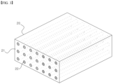
- FIG. 3 is a perspective view of an optical body 20 including a rod-shaped polymer, in which a birefringent polymer 22 elongated in a longitudinal direction inside a substrate 21 is arranged in one direction.
- a circular or elliptical birefringent polymer 22 having a cross-sectional diameter of 0. 1 ⁇ m to 0.3 ⁇ m in a longitudinal direction should be included by at least 100 million or more.
- FIG. 4 is a cross-sectional view of a birefringent island-in-the-sea yarn included in a substrate, and since the birefringent island-in-the-sea yarn can generate a light modulation effect at the optical modulation interface between the inner island portion and the sea portion, optical properties can be achieved even without arranging a very large number of island-in-the-sea yarns like the birefringent polymer described above.
- birefringent island-in-the-sea yarns are fibers, problems of compatibility with polymer substrates, ease of handling, and adhesion have occurred.
- luminance deviation occurs at any point in the plane.
- the deviation is severe, there is a problem that the image quality is markedly deteriorated, such as the appearance of spots when the image is displayed, or the desired contrast cannot be properly implemented.
- KR 2018 0111704 A , US 2010/0195313 A1 and KR 2015 0079146 A represent prior art useful for understanding the invention.
- the present invention has been devised in view of the above points, and the optical body of the present invention is capable of maximizing luminance improvement, compared to a conventional optical body, and it is an object to provide an optical body having an excellent degree of polarization and low haze, and a display device including the same.
- an object of the present invention is to provide an optical body having a uniform in-plane optical property and further having excellent optical properties, and a display device including the same.
- the optical body of the present invention is defined in claim 1 and includes a substrate and a plurality of dispersions dispersed and included inside the substrate, wherein the plurality of dispersions have an average aspect ratio of 0.5 or less, and the number of dispersions having a cross-sectional area of 0.3 ⁇ m 2 or less is 80% or more of the total dispersions.
- the number of dispersions having a cross-sectional area of 0.3 ⁇ m 2 or less may be 90% or more of the total dispersions.
- the number of dispersions having a cross-sectional area of more than 0.01 ⁇ m 2 to 0.09 ⁇ m 2 or less may be 70% to 90% of the total dispersions.
- the plurality of dispersions may have a cross-sectional dispersion coefficient of 90% to 120% according to Mathematical Formula 2 below.
- Cross ⁇ sectional dispersion coefficient % Standard deviation of cross ⁇ sectional area of dispersion Average cross ⁇ sectional area of dispersion ⁇ 100
- the optical body of the present invention is also defined in claim 4 and includes a substrate and a plurality of dispersions dispersed and included inside the substrate, and the plurality of dispersions may have an average cross-sectional area of 1 ⁇ m 2 or less and an aspect ratio dispersion coefficient of 40% or more, according to Mathematical Formula 1 below.
- Aspect ratio dispersion coefficient % Standard devision of aspect ratio of dispersion Average aspect ratio of dispersion ⁇ 100
- the plurality of dispersions may have an aspect ratio dispersion coefficient of 40% to 45% according to Mathematical Formula 1 above.
- the plurality of dispersions may have an average aspect ratio of 0.3 to 0.5.
- the optical body of the present invention may satisfy Conditions (1) and (2) below.
- the optical body of the present invention may have a haze of 25% or less.
- the optical body of the present invention may transmit a first polarized light parallel to a transmission axis and reflect a second polarized light parallel to an extinction axis.
- the optical body of the present invention may be a polymer dispersion type in which a plurality of dispersions are dispersed inside a substrate.
- the optical body of the present invention may have a luminance dispersion coefficient of 2% or less according to Mathematical Formula 3 below, which is measured based on an in-plane virtual first line parallel to the transmission axis.
- Luminance dispersion coefficient % standard deviation of luminance of samples Average luminance of samples ⁇ 100
- the optical body may be stretched in the MD direction, and the first line may be perpendicular to the MD direction.
- the luminance dispersion coefficient may be 1% or less.
- the included angle which is an acute angle with the first line may be ⁇ 60°
- the luminance dispersion coefficient which is measured based on an in-plane virtual second line passing through a bisecting point of the first line may be within 2%.
- the width when the transmission axis direction is the width direction, the width may be 85 cm or more.
- the plurality of dispersions may be stretched in one uniaxial direction and have different refractive indices in at least one axial direction from the substrate.
- the plurality of dispersions may be randomly dispersed inside the substrate.
- the display device of the present invention may include the above-mentioned optical body.
- the display device may be preferably a liquid crystal display (LCD) or a light emitting diode (LED).
- LCD liquid crystal display
- LED light emitting diode
- ⁇ dispersion has birefringence' is that when light is irradiated to a fiber having a different refractive index depending on the direction, the light incident on the dispersion is refracted by two or more lights in different directions.
- 'isotropy' means that when the light passes through an object, the refractive index is constant regardless of the direction.
- anisotropy means that the optical properties of an object are different depending on the direction of light, and anisotropic objects have birefringence and correspond to isotropy.
- ⁇ light modulation' means that the irradiated light is reflected, refracted, or scattered, or the intensity of the light, the period of the wave, or the nature of the light changes.
- ⁇ aspect ratio' refers to the ratio of a short axis length with respect to a long axis length based on the vertical cross-section in the longitudinal direction of a dispersion.
- Cross-sectional area of a dispersion' is defined by Relationship Formula 1 below.
- Cross-sectional area of dispersion ( ⁇ m 2 ) ⁇ ⁇ long axis length of dispersion / 2 ⁇ short axis length of dispersion / 2
- the long axis length and the short axis length of Relationship Formula 1 refer to the long axis and short axis of a dispersion in the cross-section of an optical body perpendicular to the elongating direction of the optical body, based on the vertical cross-section in the longitudinal direction of the dispersion (refer to FIG. 6 ).
- the optical body of the present invention and a display device including the same can not only maximize the luminance enhancement compared to the conventional optical body, but also have an excellent degree of polarization and a low haze.
- the optical body of the present invention and a display device including the same can be widely used in overall display devices such as liquid crystal display devices, organic light emitting display devices, and the like, since the in-plane optical properties are uniform, and furthermore, the optical properties are excellent.
- the optical body of the present invention may be a diffuse polarizer or a reflective polarizer. In addition, it may have various uses as a reflective polarizer, and may be useful for a liquid crystal display panel as a preferred example. In addition, the optical body of the present invention may also be used as a window material, and polarized radiation may be used as a light fixture for a preferred use.
- examples of more specific uses of the optical body of the present invention may include a light-receiving display device such as a liquid crystal display (LCD) or an active display device such as an organic light emitting display, which may be widely used in laptop computers, handheld calculators, digital watches, automotive dashboard displays, polarized luminaires, and work luminaires that use polarized light to increase contrast and reduce glare.
- a light-receiving display device such as a liquid crystal display (LCD) or an active display device such as an organic light emitting display, which may be widely used in laptop computers, handheld calculators, digital watches, automotive dashboard displays, polarized luminaires, and work luminaires that use polarized light to increase contrast and reduce glare.
- LCD liquid crystal display
- an active display device such as an organic light emitting display
- the optical body of the present invention may be used as a light extractor in various optical devices, including a light guide such as a large core optical fiber (LCOF).
- a light guide such as a large core optical fiber (LCOF).
- LCOF large core optical fiber
- it may be effectively used in high lighting of buildings, decorative lighting, medical lighting, signages, visual guides (e.g., in aisles or landing strips in airplanes or theaters), displays (e.g., particularly, device displays where excessive heat is a problem), various remote light-source lighting applications such as exhibition lighting, road lighting, automobile lighting, down lighting, work lighting, highlight lighting, and ambient lighting.
- the optical body of the present invention may transmit a first polarized light parallel to the transmission axis and reflect a second polarized light parallel to the extinction axis.
- the magnitude of the substantial coincidence or discrepancy of the refractive index of an optical body along the X, Y and Z axes in space affects the degree of scattering of polarized light rays along the axis.
- the scattering power changes in proportion to the square of the refractive index discrepancy. Therefore, the greater the degree of discrepancy of the refractive index along a particular axis is, the stronger the light rays polarized along the axis are scattered. Conversely, if the discrepancy along a particular axis is small, the light rays polarized along that axis are scattered to a lesser extent.
- the refractive index of the isotropic material of an optical body along a certain axis substantially coincides with the refractive index of an anisotropic material
- incident light polarized by an electric field parallel to this axis passes through the optical body without scattering.
- the first polarized light (P wave) is transmitted without being affected by the birefringent interface formed at the boundary between the isotropic material and the anisotropic material, but the second polarized light (S wave) is affected by a birefringent interface formed at the boundary between the isotropic material and the anisotropic material such that the modulation of light occurs.
- the P wave is transmitted, and the S wave undergoes the modulation of light such as light scattering and reflection of light such that the separation of polarized light occurs, and the first polarized light (P wave) is transmitted through the optical body and reaches a liquid crystal display which is conventionally located on top of the optical body.
- the optical body acts to transmit one polarized light and reflect the other polarized light, and the transmitted polarized light is polarized parallel to the transmission axis, and the reflected polarized light is polarized parallel to the extinction axis.
- the optical body of the present invention may be a polymer dispersion-type optical body including a substrate and a plurality of dispersions dispersed and included inside the substrate, and more preferably, it may be a random dispersion-type optical body in which a dispersion is randomly dispersed inside the substrate.
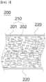
- the optical body of the present invention may be a polymer dispersion-type optical body 200 provided with a core layer 210 including a substrate 201 and a plurality of dispersions 202 dispersed and included inside the substrate, as illustrated in FIG. 5 .
- skin layers 210 and 220 may be further provided on one or both surfaces of the core layer 210, and specifically, on one or both surfaces of the substrate 201.
- the dispersion 202 may be a random dispersion-type optical body, which is randomly dispersed inside a substrate on the cross-section of the optical body perpendicular to the longitudinal direction of a plurality of dispersions, as illustrated in FIG. 5 .
- it may be a form which is uniformly arranged on the cross-section of an optical body perpendicular to the longitudinal direction of a plurality of dispersions, for example, a form in which dispersions having the same thickness are arranged in a horizontal direction at the same height of the cross-section.
- the plurality of dispersions 202 may be randomly dispersed inside the substrate. Through this, problems such as light leakage, bright line viewing, and the like may be minimized or prevented, compared to conventional optical bodies, and at the same time, it may be advantageous to express optical properties such as very good luminance, degree of polarization, and the like
- the dispersion since the dispersion must form a birefringent interface with the substrate to induce a light modulation effect, when the substrate is optically isotropic, the dispersion may have optical birefringence, and conversely, when the substrate has optical birefringence, the dispersion may have optical isotropy.
- in-plane birefringence may occur between nXi and nYi.
- At least any one of the X, Y, and Z axis refractive indices of the substrate and the dispersion may be different, and more preferably, when the elongation axis is the X axis, the difference in refractive indices with respect to the Y and Z axis directions may 0.05 or less, and the difference in the refractive indices with respect to the X-axis direction may be 0.1 or more. Meanwhile, if the difference in the refractive indices is 0.05 or less, it is conventionally interpreted as a match.
- the plurality of dispersions of the present invention may have an appropriate optical thickness to reflect the desired second polarized light in at least the visible light wavelength range, and may have a thickness deviation within an appropriate range.
- the optical thickness means that n (refractive index) > d (physical thickness).
- n refractive index
- d physical thickness
- the second polarized light having a 400 nm wavelength may be reflected by Relationship Formula 2, and when adjusting the optical thicknesses of each of the plurality of dispersions with this principle, it is possible to significantly increase the reflexibility of the second polarized light in the desired wavelength range, particularly in the visible light wavelength range.
- At least two of the plurality of dispersions may have different cross-sectional areas in the direction in which the dispersion is elongated, and through this, the cross-sectional diameter (corresponding to the optical thickness) of the dispersion may be different.
- the second polarized light having a wavelength corresponding to the optical thickness may be reflected, and when a polymer having an optical thickness corresponding to each wavelength of visible light is included, the second polarized light corresponding to the visible light region may be reflected.
- the shape of the plurality of dispersions of the present invention is not particularly limited, and may specifically be circular, elliptical, and the like, and the total number of dispersions may be 25,000,000 to 80,000,000, when the thickness of the substrate is 120 ⁇ m based on 32 inches, but is not limited thereto.
- the substrate and the dispersion of the present invention may be used without limitation as long as these are materials that are conventionally used to form a birefringent interface in an optical body
- the substrate component may preferably include one or more selected from the group consisting of polyethylene naphthalate (PEN), co-polyethylene naphthalate (co- PEN), polyethylene terephthalate (PET), polycarbonate (PC), polycarbonate (PC) alloy, polystyrene (PS), heat-resistant polystyrene (PS), polymethyl methacrylate (PMMA), polybutylene terephthalate (PBT), polypropylene (PP), polyethylene (PE), acrylonitrile butadiene styrene (ABS), polyurethane (PU), polyimide (PI), polyvinyl chloride (PVC), styrene acrylonitrile (SAN), ethylene vinyl acetate (EVA), polyamide (PA), polyacetal (POM), phenol, epoxy (EP), phenol
- polycyclohexylene dimethylene terephthalate is a compound prepared by polymerization of an acid component and a diol component at a molar ratio of 1: 0.5 to 1.5, and preferably, at a molar ratio of 1: 0.8 to 1.2.
- the acid component may include terephthalate
- the diol component may include ethyl glycol and cyclohexanedimethanol.
- the substrate component may be a material having a glass transition temperature of 110°C to 130°C, and preferably, 115°C to 125°C.
- the dispersion component may be preferably used alone with or by mixing polyethylene naphthalate (PEN), co-polyethylene naphthalate (co-PEN), polyethylene terephthalate (PET), polycarbonate (PC), polycarbonate (PC) alloy, polystyrene (PS)), heat-resistant polystyrene (PS), polymethyl methacrylate (PMMA), polybutylene terephthalate (PBT), polypropylene (PP), polyethylene (PE), acrylonitrile butadiene styrene (ABS), polyurethane (PU)), polyimide (PI), polyvinyl chloride (PVC), styrene acrylonitrile (SAN), ethylene vinyl acetate (EVA), polyamide (PA), polyacetal (POM), phenol, epoxy (EP), urea (UF), melanin (MF), unsaturated polyester (UP), silicone (SI), polycyclohexylene dimethylene terephthalate (PCTG), and
- PEN polyethylene naphthalate
- by-products may occur in the process of polymerization.
- by-products may be a residual catalyst, polyethylene glycol (PEG), and the like used in the polymerization process
- the dispersion component of the present invention may include polyethylene naphthalate (PEN), in which the content of the residual catalyst (e.g.
- Ge is 100 ppm or less, preferably, 10 ppm to 70 ppm, and more preferably, 10 ppm to 40 ppm, and the content of diethylene glycol (DEG) is 3.5 wt.% or less, preferably, 1.0 wt.% to 2.5 wt.%, and more preferably, 1.0 wt.% to 2.0 wt.%.
- DEG diethylene glycol
- polyethylene naphthalate (PEN) may have a glass transition temperature of 110°C to 125°C depending on process conditions or the molar ratio of monomers during a polymerization process
- polyethylene naphthalate (PEN) used in the present invention may have a glass transition temperature of 115°C to 125°C, preferably, 115°C to 125°C, and more preferably, 118°C to 122°C.
- optical body of the present invention satisfies Conditions (1) and (2) below.
- the optical body of the present invention may be more advantageous to achieve excellent physical properties.
- optical body of the present invention may be stretched in at least one direction to form a birefringent interface between the substrate and the dispersion.
- the plurality of dispersions of the present invention may be randomly dispersed inside the substrate.
- the optical body of the present invention may be more easily implemented to express excellent physical properties, and optical bodies that compensate for problems such as light leakage, bright light viewing, and the like may be implemented compared to conventional optical bodies.
- the random dispersion-type optical body may include a substrate and a plurality of dispersions inside the substrate for transmitting a first polarized light emitted from the outside and reflecting a second polarized light.
- the plurality of dispersions may have different refractive indices in at least one axial direction from the substrate, and the plurality of dispersions included inside the substrate may have an average aspect ratio ( ⁇ an average aspect ratio of the short axis length with respect to the long axis length based on a vertical cross-section in the longitudinal direction) of 0.5 or less, preferably, 0.3 to 0.5, more preferably, 0.4 to 0.48, and even more preferably, 0.44 to 0.46. In the case of such an optical body, it may be more advantageous to achieve excellent physical properties.
- the plurality of dispersions of the present invention may have an average cross-sectional area of 1 ⁇ m 2 or less, preferably, 0.5 ⁇ m 2 or less, and more preferably, 0.3 ⁇ m 2 or less.
- the number of dispersions having a cross-sectional area of 0.3 ⁇ m 2 or less may be 80% or more of the total dispersions, preferably, the number of dispersions having a cross-sectional area of 0.3 ⁇ m 2 or less may be 90% or more of the total dispersions, and more preferably, the number of dispersions having a cross-sectional area of 0.3 ⁇ m 2 or less may be 95% or more of the total dispersions.
- the number of dispersions having a cross-sectional area of 0.21 ⁇ m 2 or less may be 80% or more of the total dispersions, preferably, the number of dispersions having a cross-sectional area of 0.21 ⁇ m 2 or less may be 90% or more of the total dispersions, and more preferably, the number of dispersions having a cross-sectional area of 0.21 ⁇ m 2 or less may be 95% or more of the total dispersions.
- the number of dispersions having a cross-sectional area of 0. 12 ⁇ m 2 or less may be 80% or more of the total dispersions, preferably, the number of dispersions having a cross-sectional area of 0.12 ⁇ m 2 or less may be 85% or more of the total dispersions, and more preferably, the number of dispersions having a cross-sectional area of 0.12 ⁇ m 2 or less may be 93% or more of the total dispersions, and in the case of such an optical body, it may be more advantageous to achieve excellent physical properties.
- the number of dispersions having a cross-sectional area of more than 0.01 ⁇ m 2 or 0.09 ⁇ m 2 less may be 70% to 90% of the total dispersions, preferably, 75% to 85%, and more preferably, 78% to 82% of the total dispersions, and in the case of such an optical body, it may be more advantageous to achieve excellent physical properties.
- the plurality of dispersions of the present invention may have a cross-sectional dispersion coefficient of 90% to 120%, preferably 95 to 115%, and more preferably, 97 to 105% according to Mathematical Formula 2 below, and in the case of such an optical body, it may be more advantageous to achieve excellent physical properties.
- Cross ⁇ sectional dispersion coefficient % Standard deviation of cross ⁇ sectional area of dispersion Average cross ⁇ sectional area of dispersion ⁇ 100
- the cross-sectional dispersion coefficient is a parameter that can confirm the degree of dispersion of a cross-sectional area. If the cross-sectional area dispersion coefficient is 0%, it means that it is the same, and as it increases, it means that the difference in the cross-sectional area between dispersions or the ratio of the dispersions having a larger difference in the cross-sectional areas than the average cross-sectional area is increased.
- the optical body of the present invention has a very large dispersion coefficient of 90% or more for a cross-sectional area, it is composed of 80% or more of those having a cross-sectional area of 0.3 or less.
- the cross-sectional area distribution between the dispersions becomes very wide, there is an advantage that the luminance may be improved more significantly by subdividing and covering all of the desired wavelength ranges.
- the plurality of dispersions of the present invention may have an aspect ratio dispersion coefficient of 40% or more, preferably, 40% to 45%, and more preferably, 41% to 43%, according to Mathematical Formula 1 below, and in the case of such an optical body, it may be more advantageous to achieve excellent physical properties.
- Aspect ratio dispersion coefficient % Standard devision of aspect ratio of dispersion Average aspect ratio of dispersion ⁇ 100
- the haze of the random dispersion-type optical body of the present invention may be 25% or less, and preferably, 10% to 20%.
- the optical body of the present invention forms a birefringent interface between the substrate and the dispersion, and the dispersion may be stretched in at least any one direction in order to have an appropriate optical thickness.
- the uniaxial direction may be an MD direction conveyed while the optical body is continuously manufactured.
- the uniaxial direction may be a longitudinal direction that is a long axis direction of the dispersion shape.
- the polymer dispersion type in the form of the optical body of the present invention is described, it is a type of a well-known optical body along with a multilayered optical body, in which the optical layer of a flat plate formed of an optically isotropic material and the optical layer of a flat plate formed of an optically anisotropic material are alternately laminated with each other.
- the effect by the direction of force or the difference of force received by each of a plurality of dispersions when any one material of an optically isotropic material or an optically anisotropic material is expanded in one direction as the other material is dispersed and accommodated as a plurality of dispersion may be significantly greater compared to the multilayered optical body, which is a structure in which the layers of a plate are alternately laminated.
- this problem also affects impurities in the material forming an optical body, that is, catalysts and by-products used in the process of manufacturing the material, and as the size of the dispersion becomes larger, the distribution of the dispersions in the cross-section of the optical body perpendicular to the elongation direction is more random, and the problem of luminance non-uniformity becomes larger.
- the present inventors have made great efforts to control the above factors that may affect the luminance non-uniformity, and as a result, even though it is a polymer dispersion-type optical body, a reflective polarizing film having a luminance dispersion coefficient of 2% or less measured based on an in-plane virtual first line parallel to the transmission axis was implemented.
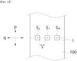
- luminance measured based on an in-plane virtual first line (l) parallel to the transmission axis (q) of the optical body 100 refers to the luminance of a specimen having a predetermined size at the center point on the first line (l).
- the transmission axis (b) may be a vertical direction of the stretched direction, or may be a TD direction when stretched in the MD direction.
- the specimen may have a circular shape or a polygonal shape such as a square or a rectangle.
- the size of the specimen may be 1 cm ⁇ 1 cm, 4 cm ⁇ 4 cm, 10 cm ⁇ 10 cm, and the like based on a square, but is not limited thereto, and it may be established in consideration of the length (e.g., the length of the width) in a direction parallel to the transmission axis (b) of the optical body 100.
- the luminance dispersion coefficient refers to the calculated result value using the average luminance and the luminance standard deviation calculated through luminances measured for each of five samples having the same shape and the same size with the center point on the first line (l) according to Mathematical Formula 3 below.
- two samples S L and S R ) are sampled in each direction of the left and right directions, centering on a first sample (S 1 ) in which the point at which the first line (l) is vertically bisected is the center of gravity of the sample, and these are sampled such that the distance between neighboring samples is the same.
- the distance between the samples refers to the distance (s) between neighboring sides of the sample, and as long as the distance between the samples is the same, the distance between the samples may be 0.
- Luminance dispersion coefficient % standard deviation of luminance of samples Average luminance of samples ⁇ 100
- the luminance dispersion coefficient is a parameter that may confirm the luminance non-uniformity between each sample. If the luminance dispersion coefficient is 0%, it means that there is no luminance difference between each sample, and it means that as the luminance dispersion coefficient becomes large, the luminance difference between each sample becomes large.
- the optical body according to the present invention has very excellent luminance uniformity as the luminance dispersion coefficient calculated by Mathematical Formula 3 is 2% or less, preferably, 1% or less, and even more preferably, 0.5% or less.
- the luminance dispersion coefficient is more than 2%, an unintended difference in contrast and the like may occur on a 32-inch or larger display, resulting in significant deterioration of image quality, and there is a concern that it will not be commercialized because it is difficult to secure the uniformity quality standard of 85% or more.
- the dispersion coefficient is more than 2%, the haze of the optical body may be significantly increased or the haze may be non-uniform for each position.
- optical properties may be deteriorated, such as a decrease in luminance and the like, and there is a concern that a thickness deviation of the optical body may occur, or appearance quality may also be remarkably deteriorated such as wrinkles, swelling phenomena, and the like.
- the optical body having a luminance dispersion coefficient of 2% or less may be implemented by, for example, improving the degree of polymerization of a material forming a dispersion or controlling impurities.
- the residual amount of a polymerization catalyst as an impurity in the substrate and/or dispersion may be 150 ppm or less, and more preferably, 100 ppm or less.
- the residual amount of a Ge catalyst, which is a polymerization catalyst may be 200 ppm or less, preferably 100 ppm or less, and more preferably 10 ppm to 70 ppm.
- the content of diethylene glycol (DEG), which is a naturally occurring by-product in the polymerization process, may be 4.0 wt.% or less, preferably, 3.5 wt.% or less, and more preferably, 1.0 wt.% to 2.0 wt.%.
- DEG diethylene glycol
- a roll having a uniform diameter in the film width direction may be used in the smoothing process of an ejected film during the manufacturing process.
- a predetermined force when stretching in the MD direction in the stretching step, a predetermined force may be constantly applied in the TD direction.
- a force may be preferably applied so as to stretch at a level of 1:1 to 1:1.2 in the TD direction.
- optical properties such as the degree of polarization, luminance, and the like may be significantly deteriorated, and if it is stretched by less than 1: 1, it may not be easy to achieve luminance uniformity.
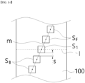
- the included angle which is an acute angle with the first line may be ⁇ 60°
- the luminance dispersion coefficient which is measured based on an in-plane virtual second line passing through a bisecting point of the first line may be 2% or less, more preferably, 1% or more, and even more preferably, 0.5% or less.
- the luminance non-uniformity problem is remarkable in a direction parallel to the transmission axis, for example, a direction perpendicular to the elongated direction, for example, in the TD direction, and for example, in the width direction, and furthermore, it may be remarkable along the first line and a predetermined angle, in particular, along the second line forming ⁇ 60° with the first line.
- these characteristics may increase the problem of luminance non-uniformity as the width of a reflective polarizing film becomes larger and the arrangement of the dispersion is random.
- the second line (m and m') passes through the center point that bisects a virtual first line (l) in the optical body 100, and it means a line segment in which the angle of the acute angle formed by the first line (l) is ⁇ 60°.
- the meaning of the luminance measured based on the second line (m or m') is the same as the luminance measured based on the first line (l) described above, and it is measured in the same manner.
- the luminance uniformity may also be a result value of the sample being sampled, measured, and calculated in the same manner.
- the optical body When the optical body satisfies not only the luminance characteristics based on the first line according to the present invention, but also the luminance characteristics based on the second line, it is possible to obtain improved luminance uniformity as well as higher haze uniformity, and thus, there is an advantage that excellent luminance characteristics may be exhibited.
- the aspect ratio of the short axis length with respect to the long axis length should be 1/2 or less based on the vertical cross-section in the longitudinal direction, and more preferably, 90% or more may satisfy the aspect ratio value of 0.5 or less. As illustrated in FIG.
- the aspect ratio is the longitudinal direction of a dispersion, that is, as one example, the MD direction, and/or as one example, when the long axis length is a and the short axis length is b in the cross-section of the dispersion in the vertical cross-section of a reflective polarizing film perpendicular to the elongation direction, the ratio (aspect ratio) of the relative length of the long axis length (a) and the short axis length (b) must be 0.5 or less. In other words, when the long axis length (a) is 2, the short axis length (b) should be less than or equal to 1. If the dispersion having an aspect ratio of 0.5 or less is less than 80%, it is difficult to achieve the desired optical properties.
- the number of dispersions having a cross-sectional area of 0.3 ⁇ m 2 or less in the plurality of dispersions may be 65% or more of the total dispersions.
- the random dispersion-type optical body of the present invention is included in the above-described substrate and the inside of the substrate, and the optical body including a plurality of dispersions satisfying the dispersion conditions according to the above-described preferred embodiment may be used as a core layer, and may have a structure including an integrated skin layer formed on at least one surface of the core layer.
- the optical body including a plurality of dispersions satisfying the dispersion conditions according to the above-described preferred embodiment may be used as a core layer, and may have a structure including an integrated skin layer formed on at least one surface of the core layer.
- by further providing a skin layer it may contribute to the protection of the core layer and the improvement of the reliability of the optical body.
- the optical body according to an embodiment that does not include a skin layer and the optical body according to another embodiment that includes a skin layer may be different in terms of use, and it may be preferable to use an optical body including a skin layer in various general-purpose liquid crystal displays such as displays and the like. Also, in the case of portable liquid crystal display devices, for example, portable electronic devices, smart electronic devices, and smartphones, it may be preferable to use an optical body that does not include a skin layer as a slim optical body is required, but is not limited thereto.
- FIG. 5 is a cross-sectional view of the random dispersion-type optical body of the present invention, and a core layer 210 in which a plurality of dispersions 202 are randomly distributed and arranged inside the substrate 201 and a skin layer 220 integrally formed on at least one surface of the core layer are shown.
- the core layer 210 may have an average aspect ratio ( ⁇ the average aspect ratio of the short axis length with respect to the major axis length based on the vertical cross-section in the longitudinal direction) of 0.5 or less, preferably, 0.3 to 0.5, more preferably, 0.4 to 0.48, and even more preferably, 0.44 to 0.46.
- ⁇ the average aspect ratio of the short axis length with respect to the major axis length based on the vertical cross-section in the longitudinal direction
- ⁇ the average aspect ratio of the short axis length with respect to the major axis length based on the vertical cross-section in the longitudinal direction
- FIG. 6 is a vertical cross-sectional view in the longitudinal direction of a dispersion used in a preferred embodiment of the present invention, and when the long axis length is a and the short axis length is b, the average of the ratio (aspect ratio) of the relative lengths of the long axis length (a) and short axis length (b) should be 0.5 or less, preferably, 0.3 to 0.5, more preferably, 0.4 to 0.48, and even more preferably, 0.44 to 0.46. If the ratio of the short axis length with respect to the long axis length does not satisfy 0.5 or less, it is difficult to achieve the desired optical properties.
- FIG. 7 is a perspective view of an optical body included in a preferred embodiment of the present invention, and a plurality of random dispersions 208 are elongated in the longitudinal direction inside the substrate 201 of the core layer 210, and the skin layer 220 may be formed above and/or below the core layer 210.
- the random dispersions 208 may be elongated in various directions, respectively, but it is advantageous to elongate in parallel in any one direction, and more preferably, it is effective to maximize the light modulation effect if it is elongated parallel between elongating bodies in a direction perpendicular to the light irradiated from an external light source.
- the thickness of a core layer may be preferably 20 ⁇ m to 350 ⁇ m, and more preferably, 50 ⁇ m to 250 ⁇ m, but is not limited thereto, and the thickness of the core layer may be designed differently depending on the specific use, whether the skin layer is included, and the thickness of the skin layer.
- the total number of dispersions may be 25,000,000 to 80,000,000, when the thickness of the substrate is 120 ⁇ m based on 32 inches, but is not limited thereto.
- a component that is conventionally used may be used for the skin layer component, and it may be used without limitation as long as it is conventionally used in a reflective polarizing film and may preferably include one or more selected from polyethylene naphthalate (PEN), co-polyethylene naphthalate (co-PEN), polyethylene terephthalate (PET), polycarbonate (PC), polycarbonate (PC) alloy, polystyrene (PS), heat-resistant polystyrene (PS), polymethyl methacrylate (PMMA), polybutylene terephthalate (PBT), polypropylene (PP), polyethylene (PE), acrylonitrile butadiene styrene (ABS), polyurethane (PU), polyimide (PI), polyvinyl chloride (PVC), styrene acrylonitrile (SAN), ethylene vinyl acetate (EVA), polyamide (PA), polyacetal (
- PEN polyethylene naphthalate
- co-PEN co-polyethylene n
- polycyclohexylene dimethylene terephthalate is a compound prepared by polymerizing an acid component and a diol component at a molar ratio of 1: 0.5 to 1.5, and preferably, 1: 0.8 to 1.2, and the acid component may include terephthalate, and the diol component may include ethyl glycol and cyclohexanedimethanol.
- the thickness of the skin layer may be 30 ⁇ m to 500 ⁇ m, but is not limited thereto.
- the width of the optical body may be 85 cm or more based on when it is manufactured.
- the width may be a length in the direction of the transmission axis, and the optical body according to the present invention has an advantage of ensuring luminance uniformity in a corresponding direction, even though it is only formed by a large area with a width of 85 cm or more.
- the optical body according to a preferred exemplary embodiment of the present invention that satisfies the above-described luminance uniformity may have a haze of 30% or less, more preferably, 25% or less, even more preferably, 22% or less, and even more preferably, 20% or less.
- the haze uniformity along the first line measured by the same sampling method of samples as the measurement method of luminance uniformity may be 3% or less, more preferably 2% or less, and even more preferably 1% or less.
- a difference in the percentages of thickness measured and calculated by the experimental method described below for the sampled sample may be within 1%.
- the skin layer when the skin layer is formed, it is integrally formed between the core layer 210 and the skin layer 220. As a result, it is possible not only to prevent deterioration of the optical properties due to the adhesive layer, but also to add more layers in a limited thickness, thereby significantly improving the optical properties. Furthermore, since the skin layer is manufactured at the same time as the core layer and then the stretching process is performed, the skin layer of the present invention may be stretched in at least one axial direction, unlike when the unstretched skin layer is adhered after stretching the core layer in the related art. Through this, surface hardness is improved compared to the unstretched skin layer, thereby improving scratch resistance and enhancing heat resistance.
- the optical body according to the present invention may further include a structured surface layer integrally at the upper or lower part of the above-described optical body, such as microlens, lenticular, prism shape, and the like for changing the path of light such as condensing or diffusion.
- a structured surface layer integrally at the upper or lower part of the above-described optical body such as microlens, lenticular, prism shape, and the like for changing the path of light such as condensing or diffusion.
- the optical body in which the above-described dispersion is randomly dispersed inside the substrate may be manufactured through a manufacturing method described below. However, it is not limited thereto.
- the substrate component and the dispersion component may be separately supplied to independent extrusion units, in which case the extrusion unit may be constituted by two or more. Also included in the present invention is that polymers are supplied to one extrusion unit including a separate supply path and a distribution port so as not to be mixed.
- the extrusion unit may be an extruder, which may further include a heating means and the like to convert the solid-phase supplied polymers into a liquid phase.
- the substrate component or the dispersion component may be advantageous in expressing luminance uniformity only when the content of impurities is less than a certain level.
- the viscosity is designed to be different such that there is a difference in polymer flowability so that the dispersion component may be arranged inside the substrate component, and preferably, the substrate component has better flowability than the dispersion component.
- an optical body in which the dispersion is randomly arranged inside the substrate may be manufactured through a difference in viscosity of the dispersion component inside the substrate.
- the skin layer component transferred from the extrusion unit is laminated on at least one surface of the optical body.
- the skin layer component may be laminated on both sides of the optical body.
- the material and thickness of the skin layers may be identical or different from each other.
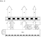
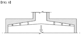
- FIG. 8 is a cross-sectional view of a coat-hanger die, which is a type of a preferred flow control unit applicable to the present invention
- FIG. 9 is a side view of FIG. 8 .
- the size and arrangement of the cross-sectional area of the dispersion component may be randomly controlled by appropriately controlling the degree of spreading of the substrate.
- the dispersion component included therein may also spread widely from left to right.
- cooling and smoothing the optical body from which the spreading is induced by the flow control unit; stretching the optical body through the smoothing step; and heat setting the stretched optical body may be further included.
- the optical body transferred from the flow control unit it may be subjected to cooling which is used in the manufacture of a conventional optical body and solidified, and then, smoothing may be performed through a casting roll process or the like.
- the roll to be used may preferably be used that has a uniform diameter, and through this, there is an advantage that luminance uniformity may be easily secured.
- the stretching may be performed through a stretching process of a conventional optical body, and through this, a difference in refractive indices between the substrate component and the dispersion component may be induced, thereby causing a light modulation phenomenon at the interface, and the first component (dispersion component) induced to spread is further reduced in the aspect ratio through stretching.
- the stretching process may preferably perform uniaxial stretching or biaxial stretching, and more preferably, it may perform uniaxial stretching.
- stretching may be performed in the longitudinal direction of a first component.
- the longitudinal direction may be the MD direction.
- the stretching ratio may be 3 times to 12 times.
- methods for changing the isotropic material to birefringence are conventionally known and, for example, when stretching under appropriate temperature conditions, the dispersion molecules are oriented such that the material may be birefringent.
- it may be easy to ensure luminance uniformity in a direction parallel to the transmission axis by controlling the stretching rate uniformly, by fixing the TD direction of the optical body that is conveyed in the MD direction and stretched with a clip, tongs, or the like, or by applying a predetermined force and stretching.
- the final optical body may be manufactured through heat setting the stretched optical body.
- the heat setting may be heat-set through a conventional method, and preferably, it may be performed through an IR heater at 180°C to 200°C for 0.1 minutes to 3 minutes.
- heat setting may be easy to ensure luminance uniformity in a direction parallel to the transmission axis by applying heat at the same level regardless of the position of the optical body.
- the optical body of the present invention described above may be employed in a light source assembly, a display device, or the like, and may be used to improve light efficiency.
- the light source assembly may be an assembly conventionally employed in work lights, lighting, or liquid crystal displays.
- the light source assembly employed in the liquid crystal display device is classified into a direct type in which the lamp is located at the bottom, an edge type in which the lamp is located at the side, and the like, and the optical body according to embodiments of the present invention may be employed in any type of light source assemblies.
- it is applicable to a backlight assembly disposed on the bottom of the liquid crystal panel or a front light assembly disposed on the top of the liquid crystal panel.
- the optical body of the present invention may be employed in an active light emitting display such as an organic light emitting display device.
- the optical body may be employed in front of the panel of an organic light emitting display device to improve a contrast ratio, enhance visibility, and the like.
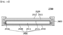
- FIG. 10 is a cross-sectional view of a liquid crystal display device according to a preferred embodiment of the present invention, and the liquid crystal display device 2700 includes a backlight unit 2400 and a liquid crystal panel assembly 2500.
- the backlight unit 2400 includes an optical body 2111 that modulates the optical characteristics of emitted light, and in this case, other components included in the backlight unit and the positional relationship between the other components and the optical body 2111 may vary depending on the purpose, and thus, it is not particularly limited in the present invention.
- a light source 2410, a light guide plate 2415 for guiding light emitted from the light source 2410, a reflective film 2320 disposed under the light guide plate 2415, and an optical body 2111 disposed on the light guide plate 2415 may be configured and positioned.
- the light source 2410 is disposed on both sides of the light guide plate 2415.
- a light emitting diode (LED), a cold cathode fluorescent lamp (CCFL), a hot cathode fluorescent lamp (HCFL), or an external electrode fluorescent lamp (EEFL) may be used.
- the light source 2410 may be disposed only on one side of the light guide plate 2415.
- the light guide plate 2415 moves light emitted from the light source 2410 through total internal reflection, and then emits light upward through a scattering pattern and the like formed on the bottom surface of the light guide plate 2415.
- a reflective film 2420 is disposed under the light guide plate 2415 to reflect light emitted downward from the light guide plate 2415 upward.
- the optical body 2111 is disposed on the light guide plate 2415. Since the optical body 2111 has been described above in detail, duplicate description is omitted. Other optical sheets may be further disposed above or below the optical body 2111. For example, a liquid crystal film partially reflecting the incident circularly polarized light, a phase-difference film for converting circularly polarized light into linearly polarized light, and/or a protective film may be further installed.
- the light source 2410, the light guide plate 2415, the reflective film 2420, and the optical body 2111 may be accommodated by a bottom chassis 2440.
- the liquid crystal panel assembly 2500 includes a first display panel 2511, a second display panel 2512, and a liquid crystal layer (not illustrated) interposed therebetween, and a polarizing plate (not illustrated) attached to the surfaces of the first display panel 2511 and the second display panel 2512 may be further included.
- the liquid crystal display 2700 may further include a top chassis 2600 covering an edge of the liquid crystal panel assembly 2500 and surrounding side surfaces of the liquid crystal panel assembly 2500 and the backlight unit 2400.
- FIG. 11 is an example of a liquid crystal display device employing an optical body according to a preferred embodiment of the present invention, in which a reflecting plate 3280 is inserted on a frame 3270, and a cold cathode fluorescent lamp 3290 is positioned on the upper surface of the reflecting plate 3280.
- An optical film 3320 is located on the upper surface of the cold cathode fluorescent lamp 3290, and the optical film 3320 may be laminated in the order of a diffusion plate 3321, an optical body 3322, and an absorption polarizing film 3323.
- the components included in the optical film and the laminating order between the components may vary depending on the purpose, and some components may be omitted or provided in a plurality.
- a phase-difference film (not illustrated) or the like may also be inserted at an appropriate position in the liquid crystal display device.
- a liquid crystal display panel 3310 may be positioned on the upper surface of the optical film 3320 to be fitted into a mold frame 3300.
- the diffusion plate 3321 in the optical film 3320 Light transmitted through the diffusion plate 3321 passes through the optical body 3322 in order to propagate the light traveling direction vertically with respect to the optical film 3320, thereby causing light modulation.
- the P wave transmits the optical body without loss, but in the case of the S wave, light modulation (reflection, scattering, refraction, etc. ) occurs, and it is reflected by a reflector 3280 again, which is the back side of the cold cathode fluorescent lamp 3290.
- the properties of light are randomly changed to the P wave or S wave, it passes through the optical body 3322 again.
- the cold cathode fluorescent lamp 3290 may be replaced with LED.
- an optical body by applying an optical body according to embodiments of the present invention, there are advantages that a plurality of light modulation characteristics may be effectively exhibited, luminance may be improved, and light leakage and bright lines do not occur, and it may prevent appearance defects in which foreign substances appear on the exterior, and at the same time, it is possible to ensure the reliability of the optical body even in a high temperature and high humidity environment where a liquid crystal display is used.
- the micropattern layer and the light-collecting layer having respective functions are integrated into the optical body, thereby reducing the thickness of the light source assembly.
- the assembly process may be simplified, and the image quality of the liquid crystal display device including such a light source assembly may be improved.
- the use of the optical body has been mainly described for liquid crystal displays, but is not limited thereto, and it can be widely used in flat panel display technologies such as projection displays, plasma displays, field emission displays, and electroluminescent displays.
- Example 1 Manufacture of random dispersion-type optical body
- PEN polyethylene naphthalate
- PCTG polycyclohexylene dimethylene terephthalate
- terephthalate as an acid component and ethyl glycol and cyclohexanedimethanol as diol components were polymerized at a molar ratio of 1:2
- H 3 PO 3 phosphorous acid
- polyethylene naphthalate polyethylene naphthalate (PEN) including 30 ppm of the residual amount of a Ge catalyst used in the polymerization process, and 1.5 wt.% of diethylene glycol (DEG), which is a polymerization by-product, was used.
- DEG diethylene glycol
- the extrusion temperature of the substrate component and the dispersion component was set to 245°C, and the Cap. Rheometer was checked to correct the polymer flow through I.V adjustment.
- the dispersion was induced to be randomly dispersed inside the substrate by passing through the flow path to which the filtration mixer was applied, and the substrate layer polymer was induced to spread in the coat hanger dies of FIGS. 8 and 9 to correct the flow rate and pressure gradient.
- the width of a die inlet was 200 mm, and the thickness was 10 mm.
- the width of a die outlet was 1,260 mm
- the thickness was 2.5 mm
- the flow rate was 1.0 m/min.
- a smoothing process was performed on the cooling and casting rolls, and it was stretched 6 times in the MD direction.
- heat setting was performed through a heater chamber at 180°C for 2 minutes to manufacture a random dispersion-type optical body having a thickness of 120 ⁇ m with a cross-sectional structure as shown in FIG. 5 .
- the refractive index of the dispersion component of the manufactured optical body was (nx: 1.88, ny: 1.58, nz: 1.58), and the refractive index of the substrate component was 1.58.
- Example 2 Manufacture of random dispersion-type optical body
- Example 2 In the same manner as in Example 1, a random dispersion-type optical body having a cross-sectional structure as shown in FIG. 5 and an average aspect ratio and cross-sectional area of the dispersion as shown in Table 1 was manufactured.
- polyethylene naphthalate (PEN) used as a dispersion component polyethylene naphthalate (PEN) including 45 ppm of the residual amount of a Ge catalyst used in the polymerization process and 2.0 wt.% of diethylene glycol (DEG), which was a polymerization by-product, was used.
- DEG diethylene glycol
- Example 3 Manufacture of random dispersion-type optical body
- Example 2 In the same manner as in Example 1, a random dispersion-type optical body having a cross-sectional structure as shown in FIG. 5 was manufactured.
- polyethylene naphthalate (PEN) used as a dispersion component polyethylene naphthalate (PEN) including 80 ppm of the residual amount of a Ge catalyst used in the polymerization process and 3.0 wt.% of diethylene glycol (DEG), which was a polymerization by-product, was used.
- DEG diethylene glycol
- Comparative Example 1 Manufacture of random dispersion-type optical body
- Example 2 In the same manner as in Example 1, a random dispersion-type optical body having a cross-sectional structure as shown in FIG. 5 was manufactured.
- polyethylene naphthalate (PEN) used as a dispersion component polyethylene naphthalate (PEN) including 140 ppm of the residual amount of a Ge catalyst used in the polymerization process and 3.0 wt.% of diethylene glycol (DEG), which was a polymerization by-product, was used.
- DEG diethylene glycol
- the relative luminance represents the relative values of the luminances of the other Examples and Comparative Examples, when the luminance of the optical body of Example 1 was set to 100 (reference).
- Haze was measured using the analysis equipment of a haze and transmittance measurement device (COH-400 which is a product of Nippon Denshoku Kogyo Co.).
- the aspect ratio was calculated by measuring the length in a longitudinal direction and the length in a transverse direction for each dispersion included in the cross-sectional photograph.
- the reliability of the numerical values for the cross-sectional area was secured by targeting those with a number of dispersions of 1,000 or more in the cross-sectional photograph.
- the long axis length and the short axis length of the dispersion in Relationship Formula 1 refer the long axis and the short axis of the dispersion in the cross-section of the optical body perpendicular to the elongation direction of the optical body.
- Comparative Example 2 Random dispersion-type optical body manufactured in Example 1 of Korean Patent Application No. 10-2013-0169215
- Example 1 of Korean Patent Application No. 10-2013-0169215 a random dispersion-type optical body was manufactured, and the manufactured random dispersion-type optical body was confirmed to have the physical property values described in Table 2 below through the above experimental example.
- Table 2 Classification Comparative Example 2 Remarks Group 1 48% of total dispersions Among the dispersions with an aspect ratio of 1/2 or less, the cross-sectional area of Group 1 is 0.2 to 2.0 ⁇ m 2 , the cross-sectional area of Group 2 is more than 2.0 ⁇ m 2 to 5.0 ⁇ m 2 or less, and the cross-sectional area of Group 3 is more than 5.0 ⁇ m 2 to 10.0 ⁇ m 2 or less Group 2 40% of total dispersions Group 3 12% of total dispersions Relative luminance 89 Haze (%) 29% Degree of polarization 82%
- the optical bodies manufactured in Examples 1 to 3 not only had superior luminance values compared to the optical bodies manufactured in Comparative Examples 1 to 2, but also had low haze values and excellent degrees of polarization.
- the optical bodies manufactured in Example 1 not only had the most excellent luminance value, but also had a low haze value and excellent degree of polarization.
- a random dispersion-type optical body was manufactured in the same manner as in Example 1.
- PEN polyethylene naphthalate
- PCTG polycyclohexylene dimethylene terephthalate
- terephthalate as an acid component and ethyl glycol and cyclohexanedimethanol as diol components were polymerized at a molar ratio of 1:2
- H 3 PO 3 phosphorous acid
- polyethylene naphthalate polyethylene naphthalate (PEN) including 30 ppm of the residual amount of a Ge catalyst used in the polymerization process and 1.5 wt.% of diethylene glycol (DEG), which is a polymerization by-product, was used.
- DEG diethylene glycol
- a random dispersion type optical body was manufactured in the same manner as in Example 1.
- PEN polyethylene naphthalate
- PCTG polycyclohexylene dimethylene terephthalate
- H 3 PO 3 phosphorous acid
- polyethylene naphthalate polyethylene naphthalate (PEN) including 30 ppm of the residual amount of a Ge catalyst used in the polymerization process and 1.5 wt.% of diethylene glycol (DEG), which is a polymerization by-product, was used.
- DEG diethylene glycol
- a random dispersion-type optical body was manufactured in the same manner as in Example 1.
- PEN polyethylene naphthalate
- PCTG polycyclohexylene dimethylene terephthalate
- terephthalate as an acid component and ethyl glycol and cyclohexanedimethanol as diol components were polymerized at a molar ratio of 1:2
- H 3 PO 3 phosphorous acid
- polyethylene naphthalate polyethylene naphthalate (PEN) including 30 ppm of the residual amount of a Ge catalyst used in the polymerization process and 1.5 wt.% of diethylene glycol (DEG), which is a polymerization by-product, was used.
- DEG diethylene glycol
- the relative luminance represents the relative values of the luminances of the other Examples and Comparative Examples, when the luminance of the optical body of Example 1 was set to 100 (reference).
- the optical bodies manufactured in Examples 1 and 4 not only had superior luminance values compared to the optical bodies manufactured in Comparative Examples 3 to 5, but also had low haze values and excellent degrees of polarization.
- the optical bodies manufactured in Example 1 not only had the most excellent luminance value, but also had a low haze value and excellent degree of polarization.
- PCTG polycyclohexylene dimethylene terephthalate
- PEN polyethylene naphthalate
- DEG diethylene glycol
- the extrusion temperature of the substrate component and the dispersion component was set to 245°C, and the Cap. Rheometer was checked to correct the polymer flow through I.V adjustment.
- the dispersion was induced to be randomly dispersed inside the substrate by passing through the flow path to which the filtration mixer was applied, and the substrate layer polymer was induced to spread in the coat hanger dies of FIGS. 8 and 9 to correct the flow rate and pressure gradient.
- the flow rate was 1.0 m/min.
- a smoothing process was performed on the cooling and casting rolls. Then, it was stretched 6 times in the MD direction, and at this time, a predetermined force was applied in the TD direction to stretch in the MD direction by 1.1 times while being stretched.
- PEN polyethylene naphthalate
- DEG diethylene glycol
- a multilayer reflective polarizer in which PEN and a PC alloy were alternately laminated with each of plate-like optical layers was manufactured.
- PEN polyethylene naphthalate
- DEG diethylene glycol
- Korean Patent Application No. 10-2012-0087416 by the same applicant of the present invention is incorporated herein by reference.
- PEN as a dispersion, a substrate, and a PC alloy as a skin layer were respectively introduced into the first extrusion unit, the second extrusion unit, and the third extrusion unit.
- the extrusion temperature of PEN and the PC alloy was set to 295°C, and the Cap. Rheometer was checked to correct the polymer flow through I.V adjustment, and an extrusion process was performed for the skin layer at a temperature level of 280°C.
- One slit-type extrusion mold consisted of 300 layers, the thickness of the slit of the first slit-type extrusion mold of the bottom surface of the fifth mold distribution plate of FIG.
- the four multilayered composites discharged through the four slit-type extrusion molds and the skin layer components conveyed through separate passages were laminated in a collection block to be laminated into a single core layer and a skin layer integrally formed on both sides of the core layer.
- the core layer polymer on which the skin layer was formed was induced to spread in the coat hanger dies of FIGS. 8 and 9 to correct the flow rate and pressure gradient.
- the flow rate was 1 m/min.
- a smoothing process was performed on the cooling and casting rolls, and it was stretched 6 times in the MD direction, and at this time, no force was applied in the TD direction.
- heat setting was performed through an IR heater at 180°C for 2 minutes to manufacture a multilayer reflective polarizer as shown in FIG. 16 .
- the refractive index of the first component of the manufactured reflective polarizer was (nx: 1.88, ny: 1.64, nz: 1.64), and the refractive index of the second component was 1.64.
- Group A had 300 layers (150 repeating units), and the repeating unit had a thickness of 168 nm, an average optical thickness of 275.5 nm, and an optical thickness deviation within 20%.
- Group B had 300 layers (150 repeating units), and the repeating unit had a thickness of 138 nm, an average optical thickness of 226.3 nm, and an optical thickness deviation within 20%.
- Group C had 300 layers (150 repeating units), and the repeating unit had a thickness of 110 nm, an average optical thickness of 180.4 nm, and an optical thickness deviation within 20%.
- Group D had 300 layers (150 repeat units), and the repeating unit had a thickness of 200 nm, an average optical thickness of 328 nm, and an optical thickness deviation within 20%.
- the manufactured multilayer reflective polarizer had a core layer thickness of 92.4 ⁇ m and a skin layer thickness of 153.8 ⁇ m, respectively, with a total thickness of 400 ⁇ m and a total width of 98 cm.
- An arbitrary first line parallel to the transmission axis of the manufactured optical body was selected, and a total of five samples having a size of 100 mm ⁇ 100 mm of a square having a center point on the first line were sampled.
- two samples in the left direction and two samples in the right direction were sampled, centering on the first sample having the center point at a point where the first line was vertically bisected, but the distance between adjacent samples was 50 mm.
- luminance at 9 points was measured using Topcon's BM-7 measurement device to show the average value.
- the backlight unit was manufactured and used to match the size of the sample.
- Luminance dispersion coefficient % standard deviation of luminance of samples Average luminance of samples ⁇ 100
- Example 5 the average luminance of Example 5 was based on 100%, and the average luminance of the remaining Examples and Comparative Examples was shown as relative luminance.
- the length in the longitudinal direction of each dispersion included in the cross-sectional photograph and the length in the transverse direction were measured to calculate the aspect ratio.
- the reliability of the numerical values for the cross-sectional area was secured by targeting those with a number of dispersions of 1,000 or more in the cross-sectional photograph.
- the thickness based on the center point of each sample that was sampled was measured, and then, the thickness percentage of other samples was calculated based on the sample thickness of the maximum thickness as 100%. After counting the number of samples with a thickness percentage difference exceeding 1%, the excess number was evaluated as 5 points for 0, 4 points for 1, 3 points for 2, 2 points for 3, and 1 point for 4.
- Comparative Example 8 which is a multilayer optical body, it was confirmed that the content of by-products in the polymer chip forming the layer was high, and the luminance uniformity based on the first line or the second line was excellent, even when there was no treatment in the TD direction.
- Example 5 and Comparative Examples 6 to 7, which are polymer dispersion-type optical fibers including dispersions it could be confirmed that the luminance uniformity was significantly changed by various factors such as width, the content of by-products, the cross-sectional area, and the like.
- Comparative Examples 6 and 7 are compared, it could be confirmed that in the case of Comparative Example 6 having a width of 85 cm or more, a problem of luminance uniformity was further generated compared to Comparative Example 7.
- the present invention relates to an optical body and a display device including the same, and more particularly, the present invention relates to an optical body capable of maximizing luminance improvement of the optical body while minimizing optical loss of the optical body, and a display device including the same.
Landscapes
- Physics & Mathematics (AREA)
- General Physics & Mathematics (AREA)
- Optics & Photonics (AREA)
- Nonlinear Science (AREA)
- Chemical & Material Sciences (AREA)
- Crystallography & Structural Chemistry (AREA)
- Mathematical Physics (AREA)
- Engineering & Computer Science (AREA)
- Manufacturing & Machinery (AREA)
- Polarising Elements (AREA)
- Liquid Crystal (AREA)
- Optical Elements Other Than Lenses (AREA)
Claims (10)
- Optischer Körper (2111), umfassend:ein Substrat (201); undeine Vielzahl von Dispersionen (208), die innerhalb des Substrats (201) dispergiert und umfasst sind, wobei die Dispersionen eine doppelbrechende Schnittstelle mit dem Substrat bilden,
wobei die Vielzahl von Dispersionen (208) ein durchschnittliches Seitenverhältnis von 0,5 oder weniger aufweisen, wobei das Seitenverhältnis das Verhältnis einer Nebenachsenlänge zu einer Hauptachsenlänge basierend auf einem vertikalen Querschnitt in einer Längsachse einer Dispersion ist, und dadurch gekennzeichnet, dass die Anzahl von Dispersionen (208) eine Querschnittfläche von 0,3 µm2 oder weniger 80 % oder mehr der gesamten Dispersionen (208) aufweist, wobei die Querschnittfläche einer Dispersion durch die Beziehungsformel definiert ist:Querschnittfläche der Dispersion (µm2) = π × Länge der Dispersionslängsachse / 2 × kurze Achsenlänge der Dispersion / 2und wobei die Länge der langen Achse und die Länge der kurzen Achse der Beziehungsformel 1 die lange Achse und kurze Achse einer Dispersion im Querschnitt eines optischen Körpers senkrecht zu der Ausdehnungsrichtung des optischen Körpers, basierend auf dem vertikalen Querschnitt in Längsrichtung der Dispersion, bezeichnen,und wobei der optische Körper (2111) die nachstehenden Bedingungen (1) und (2) erfüllt.(1) Glasübergangstemperatur (Tg) der Dispersion > Glasübergangstemperatur (Tg) des Substrats(2) Der Unterschied zwischen den Glasübergangstemperaturen einer Dispersion und eines Substrats liegt innerhalb des Bereichs von 3 bis 9 °C, und wobei die Glasübergangstemperatur (Tg) des Substrats 110 °C bis 130 °C beträgt. - Optischer Körper nach Anspruch 1, wobei in der Vielzahl von Dispersionen (208) die Anzahl der Dispersionen (208), die eine Querschnittfläche von mehr als 0,01 µm2 bis 0,09 µm2 oder weniger aufweisen, 70 % bis 90 % der gesamten Dispersionen ausmachen.
- Optischer Körper nach Anspruch 1, wobei die Vielzahl von Dispersionen (208) einen Querschnittdispersionskoeffizienten von 90 % bis 120 % gemäß der nachstehenden mathematischen Formel 2 aufweisen.

- Optischer Körper (2111), umfassend:ein Substrat (201); undeine Vielzahl von Dispersionen (208), die innerhalb des Substrats dispergiert und umfasst sind,wobei die Dispersionen eine doppelbrechende Schnittstelle mit dem Substrat bilden und wobei die Vielzahl von Dispersionen eine durchschnittliche Querschnittfläche von 1 µm2 oder weniger aufweist, wobei die Querschnittfläche einer Dispersion durch die Beziehungsformel definiert ist:Querschnittfläche der Dispersion (µm2) = π × Länge der Dispersionslängsachse / 2 × kurze Achsenlänge der Dispersion / 2und wobei die Länge der langen Achse und die Länge der kurzen Achse der Beziehungsformel 1 die lange Achse und kurze Achse einer Dispersion im Querschnitt eines optischen Körpers senkrecht zu der Ausdehnungsrichtung des optischen Körpers, basierend auf dem vertikalen Querschnitt in Längsrichtung der Dispersion, bezeichnen,und dadurch gekennzeichnet, dass ein Seitenverhältnis-Dispersionskoeffizient von 40 % oder mehr gemäß der nachstehenden mathematischen Formel 1 vorliegt.
 wobei das Seitenverhältnis das Verhältnis einer Nebenachsenlänge zu einer Hauptachsenlänge basierend auf einem vertikalen Querschnitt in einer Längsachse einer Dispersion ist,und wobei der optische Körper (2111) die nachstehenden Bedingungen (1) und (2) erfüllt.(1) Glasübergangstemperatur (Tg) der Dispersion > Glasübergangstemperatur (Tg) des Substrats und(2) Der Unterschied zwischen den Glasübergangstemperaturen einer Dispersion und eines Substrats liegt innerhalb des Bereichs von 3 bis 9 °C, und wobei die Glasübergangstemperatur (Tg) des Substrats 110 °C bis 130 °C beträgt.
 - Optischer Körper nach Anspruch 4, wobei die Vielzahl von Dispersionen (208) ein durchschnittliches Seitenverhältnis von 0,3 bis 0,5 aufweist.
- Optischer Körper nach Anspruch 1 oder 4, wobei der optische Körper (2111) eine Trübung von 25 % oder weniger aufweist.
- Optischer Körper nach Anspruch 1 oder 4, wobei der optische Körper (2111) ein erstes polarisiertes Licht parallel zu einer Übertragungsachse überträgt und ein zweites polarisiertes Licht parallel zu einer Extinktionsachse reflektiert.
- Optischer Körper nach Anspruch 7, wobei der optische Körper (2111) einen Leuchtdichtedispersionskoeffizienten von 2% oder weniger gemäß der nachstehenden mathematischen Formel 3 aufweist, die basierend auf einer virtuellen ersten Linie in der Ebene parallel zu der Übertragungsachse gemessen wird, und wobei der Leuchtdichtedispersionskoeffizienten den berechneten Ergebniswert unter Verwendung der durchschnittlichen Leuchtdichte und der Leuchtdichtestandardabweichung bezeichnet, die durch die Leuchtdichtemessung für fünf Probenflächen berechnet wird, wobei die Probenflächen als Proben in der mathematischen Formel 3 definiert sind und die gleiche Form und die gleiche Größe mit dem Mittelpunkt auf der ersten Linie (f|) aufweisen.
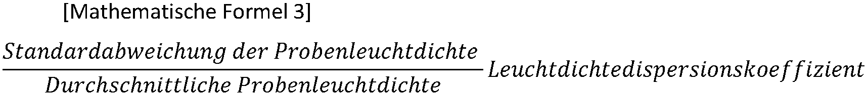
- Optischer Körper (2111) nach Anspruch 8, wobei der eingeschlossene Winkel, der ein spitzer Winkel mit der ersten Linie ist, ±60° beträgt, und der Leuchtdichtedispersionskoeffizient, der basierend auf einer virtuellen zweiten Linie in der Ebene, die durch einen Halbierungspunkt der ersten Linie verläuft, gemessen wird, innerhalb von 2% liegt.
- Anzeigevorrichtung, die den optischen Körper nach Anspruch 1 oder 4 umfasst.
Applications Claiming Priority (5)
| Application Number | Priority Date | Filing Date | Title |
|---|---|---|---|
| KR1020180145594A KR102698463B1 (ko) | 2018-11-22 | 2018-11-22 | 광학체 및 이를 포함하는 표시장치 |
| KR1020180145536A KR102698488B1 (ko) | 2018-11-22 | 2018-11-22 | 광학체 및 이를 포함하는 표시장치 |
| KR1020180145535A KR102540191B1 (ko) | 2018-11-22 | 2018-11-22 | 광학체 및 이를 포함하는 표시장치 |
| KR1020180147451A KR102551104B1 (ko) | 2018-11-26 | 2018-11-26 | 반사편광필름 및 이를 포함하는 표시장치 |
| PCT/KR2019/015335 WO2020105931A1 (ko) | 2018-11-22 | 2019-11-12 | 광학체 및 이를 포함하는 표시장치 |
Publications (4)
| Publication Number | Publication Date |
|---|---|
| EP3885802A1 EP3885802A1 (de) | 2021-09-29 |
| EP3885802A4 EP3885802A4 (de) | 2022-08-24 |
| EP3885802B1 true EP3885802B1 (de) | 2025-01-15 |
| EP3885802C0 EP3885802C0 (de) | 2025-01-15 |
Family
ID=70773297
Family Applications (1)
| Application Number | Title | Priority Date | Filing Date |
|---|---|---|---|
| EP19886144.5A Active EP3885802B1 (de) | 2018-11-22 | 2019-11-12 | Optischer körper und anzeigevorrichtung damit |
Country Status (4)
| Country | Link |
|---|---|
| US (1) | US12111532B2 (de) |
| EP (1) | EP3885802B1 (de) |
| TW (1) | TWI721662B (de) |
| WO (1) | WO2020105931A1 (de) |
Families Citing this family (8)
| Publication number | Priority date | Publication date | Assignee | Title |
|---|---|---|---|---|
| KR102102040B1 (ko) | 2018-07-31 | 2020-04-17 | 도레이첨단소재 주식회사 | 내오염성 역삼투 분리막, 이의 제조방법 및 이를 포함하는 내오염성 역삼투 모듈 |
| KR102235399B1 (ko) | 2019-09-17 | 2021-04-01 | 도레이첨단소재 주식회사 | 선택형 양단 집수기능을 갖는 필터 구조체 및 이를 이용한 여과방법 |
| KR102816001B1 (ko) | 2019-09-18 | 2025-05-30 | 도레이첨단소재 주식회사 | 역삼투막 및 이의 제조방법 |
| KR102172284B1 (ko) | 2019-10-29 | 2020-10-30 | 도레이첨단소재 주식회사 | 나권형 분리막 모듈 및 이의 제조방법 |
| KR102251754B1 (ko) | 2019-12-24 | 2021-05-12 | 도레이첨단소재 주식회사 | 기계적 강도가 향상된 부직포 |
| KR102347498B1 (ko) | 2020-04-17 | 2022-01-05 | 도레이첨단소재 주식회사 | 중금속 비용출성 나권형 필터 모듈 및 이의 제조방법 |
| KR102687943B1 (ko) * | 2021-10-05 | 2024-07-23 | 도레이첨단소재 주식회사 | 반사편광필름, 이를 포함하는 광원 어셈블리 및 액정표시장치 |
| TWI807616B (zh) * | 2022-01-26 | 2023-07-01 | 友達光電股份有限公司 | 畫素陣列基板 |
Family Cites Families (37)
| Publication number | Priority date | Publication date | Assignee | Title |
|---|---|---|---|---|
| JP2505631B2 (ja) | 1990-08-09 | 1996-06-12 | 東レ株式会社 | 複合半透膜およびその製造方法および高純度水の製造方法 |
| JP3559475B2 (ja) | 1999-06-15 | 2004-09-02 | 日東電工株式会社 | 液体分離膜モジュール |
| JP4705746B2 (ja) | 2000-05-23 | 2011-06-22 | ジーイー・オズモニクス・インコーポレイテッド | ナノ濾過のための酸安定性膜 |
| DE10292319B4 (de) * | 2001-06-01 | 2012-03-08 | Daicel Chemical Industries, Ltd. | Lichtstreuender Film, ebene Lichtquellen-Einrichtung und Flüssigkristall-Anzeige-Vorrichtung, in denen er verwendet wird |
| JP2006251395A (ja) * | 2005-03-10 | 2006-09-21 | Daicel Chem Ind Ltd | 異方性散乱シート |
| JP4606299B2 (ja) | 2005-10-19 | 2011-01-05 | オルガノ株式会社 | 分離膜の改質方法および装置並びにその方法により改質された分離膜 |
| JP4488431B2 (ja) | 2005-12-22 | 2010-06-23 | 日東電工株式会社 | スパイラル型分離膜エレメント |
| KR101395366B1 (ko) | 2007-02-05 | 2014-05-14 | 다우 글로벌 테크놀로지스 엘엘씨 | 개질된 폴리아마이드 막 |
| US7677780B2 (en) | 2007-02-20 | 2010-03-16 | 3M Innovative Properties Company | Light guide orientation connector |
| JP5244797B2 (ja) * | 2007-08-02 | 2013-07-24 | 株式会社ダイセル | 光拡散フィルム及びそれを備えた装置 |
| JP2009045595A (ja) | 2007-08-22 | 2009-03-05 | Nitto Denko Corp | 複合逆浸透膜及びこれを用いた膜分離方法 |
| JP5165362B2 (ja) | 2007-12-21 | 2013-03-21 | 花王株式会社 | 抗菌剤 |
| KR101532462B1 (ko) | 2008-01-31 | 2015-06-29 | 닛토덴코 가부시키가이샤 | 편광자 보호 필름, 편광판 및 화상 표시 장치 |
| KR101357380B1 (ko) | 2008-10-07 | 2014-02-03 | 다이니폰 인사츠 가부시키가이샤 | 광학 시트, 면 광원 장치 및 투과형 표시 장치 |
| JP2011005455A (ja) | 2009-06-29 | 2011-01-13 | Toray Ind Inc | 分離膜支持体並びにそれを用いた分離膜および膜分離エレメント |
| JP5932652B2 (ja) | 2009-10-24 | 2016-06-08 | スリーエム イノベイティブ プロパティズ カンパニー | 光学構造物 |
| KR20120087416A (ko) | 2011-01-28 | 2012-08-07 | 안종환 | 마그네틱 자철분을 이용한 소형 공작물의 고정 |
| WO2013129610A1 (ja) | 2012-02-29 | 2013-09-06 | 東レ株式会社 | 複合半透膜 |
| KR101931378B1 (ko) | 2012-08-09 | 2018-12-20 | 도레이케미칼 주식회사 | 다층 반사편광자의 제조방법 및 장치 |
| KR101944118B1 (ko) | 2012-10-11 | 2019-01-30 | 도레이케미칼 주식회사 | 내오염 성능이 우수한 역삼투 복합막 및 그 제조방법 |
| JP5981300B2 (ja) | 2012-10-25 | 2016-08-31 | 帝人株式会社 | 分離膜支持体およびその製造方法 |
| KR102172281B1 (ko) | 2013-12-27 | 2020-10-30 | 도레이첨단소재 주식회사 | 층간접착력이 우수한 정삼투막 및 그 제조방법 |
| KR102172539B1 (ko) | 2013-12-31 | 2020-10-30 | 도레이첨단소재 주식회사 | 랜덤 분산형 반사 편광자 |
| KR102127018B1 (ko) | 2013-12-31 | 2020-06-25 | 도레이첨단소재 주식회사 | 분산형 반사편광자용 보상층 조성물 및 이를 이용한 분산형 반사편광자 |
| KR102172288B1 (ko) | 2013-12-31 | 2020-10-30 | 도레이첨단소재 주식회사 | 랜덤 분산형 반사 편광자 |
| KR101790533B1 (ko) | 2014-12-31 | 2017-10-26 | 도레이케미칼 주식회사 | 반사편광자 및 이를 포함하는 백라이트 유닛 |
| JP6575154B2 (ja) | 2015-06-09 | 2019-09-18 | 東レ株式会社 | トリコット流路材 |
| GB2540572B (en) | 2015-07-21 | 2018-12-19 | Dyson Technology Ltd | Battery charger |
| JP6552959B2 (ja) | 2015-12-28 | 2019-07-31 | Kbセーレン株式会社 | 嗜好性飲料抽出フィルター用織物 |
| KR102471008B1 (ko) | 2016-03-04 | 2022-11-24 | 도레이첨단소재 주식회사 | 안티몬 비용출 심초형 복합섬유 및 이를 포함하는 안티몬 비용출 트리코트 여과직물 |
| CN105694053B (zh) | 2016-03-16 | 2018-09-11 | 泉州亚林新材料科技有限公司 | 一种季铵盐改性壳聚糖抗菌剂及其制备方法和应用 |
| KR101867870B1 (ko) | 2016-03-29 | 2018-06-18 | 주식회사 엠씨엠 | 나권형 필터 카트리지의 제조방법 |
| CN105771672B (zh) | 2016-04-18 | 2018-03-02 | 天津工业大学 | 一种抗污染抗菌芳香聚酰胺反渗透复合膜及制备方法 |
| KR102045108B1 (ko) | 2016-05-10 | 2019-11-14 | 주식회사 엘지화학 | 역삼투막 및 그 제조방법 |
| KR102385165B1 (ko) | 2017-03-31 | 2022-04-11 | 도레이첨단소재 주식회사 | 반사편광필름, 이를 포함하는 광원 어셈블리 및 액정표시장치 |
| KR102102040B1 (ko) | 2018-07-31 | 2020-04-17 | 도레이첨단소재 주식회사 | 내오염성 역삼투 분리막, 이의 제조방법 및 이를 포함하는 내오염성 역삼투 모듈 |
| KR102347498B1 (ko) | 2020-04-17 | 2022-01-05 | 도레이첨단소재 주식회사 | 중금속 비용출성 나권형 필터 모듈 및 이의 제조방법 |
-
2019
- 2019-11-12 EP EP19886144.5A patent/EP3885802B1/de active Active
- 2019-11-12 WO PCT/KR2019/015335 patent/WO2020105931A1/ko not_active Ceased
- 2019-11-12 US US17/294,999 patent/US12111532B2/en active Active
- 2019-11-22 TW TW108142458A patent/TWI721662B/zh active
Also Published As
| Publication number | Publication date |
|---|---|
| TW202019672A (zh) | 2020-06-01 |
| US12111532B2 (en) | 2024-10-08 |
| US20220011630A1 (en) | 2022-01-13 |
| EP3885802A1 (de) | 2021-09-29 |
| EP3885802A4 (de) | 2022-08-24 |
| TWI721662B (zh) | 2021-03-11 |
| WO2020105931A1 (ko) | 2020-05-28 |
| EP3885802C0 (de) | 2025-01-15 |
Similar Documents
| Publication | Publication Date | Title |
|---|---|---|
| EP3885802B1 (de) | Optischer körper und anzeigevorrichtung damit | |
| KR101201256B1 (ko) | 폴리머가 분산된 반사 편광자 제조방법 및 장치 | |
| KR102172539B1 (ko) | 랜덤 분산형 반사 편광자 | |
| KR102385165B1 (ko) | 반사편광필름, 이를 포함하는 광원 어셈블리 및 액정표시장치 | |
| TWI606284B (zh) | 隨機散布式反射偏光器 | |
| CN105874362B (zh) | 随机散布式反射偏光器 | |
| KR102698488B1 (ko) | 광학체 및 이를 포함하는 표시장치 | |
| KR102172288B1 (ko) | 랜덤 분산형 반사 편광자 | |
| US20250020957A1 (en) | Reflective polarizing film, and light source assembly and liquid display device each comprising same | |
| KR20180111327A (ko) | 복합편광필름, 이의 제조방법, 이를 포함하는 광원 어셈블리 및 액정표시장치 | |
| KR102698461B1 (ko) | 광학체 및 이를 포함하는 표시장치 | |
| KR20140021233A (ko) | 다층 반사편광자의 제조방법 및 장치 | |
| KR102540191B1 (ko) | 광학체 및 이를 포함하는 표시장치 | |
| KR102227678B1 (ko) | 광학체 및 이를 포함하는 표시장치 | |
| KR102698463B1 (ko) | 광학체 및 이를 포함하는 표시장치 | |
| KR102551104B1 (ko) | 반사편광필름 및 이를 포함하는 표시장치 | |
| KR101714388B1 (ko) | 반사편광 필름 및 그 제조방법 | |
| KR20140021253A (ko) | 폴리머가 분산된 반사 편광자 제조방법 및 장치 | |
| KR20140021239A (ko) | 다층 반사편광자의 제조방법 및 장치 | |
| KR20140021254A (ko) | 다층 반사편광자의 제조방법 및 장치 | |
| KR20140021240A (ko) | 폴리머가 분산된 반사 편광자 제조방법 및 장치 | |
| KR20140021247A (ko) | 다층 반사편광자의 제조방법 및 장치 | |
| KR20140021238A (ko) | 폴리머가 분산된 반사 편광자 제조방법 및 장치 |
Legal Events
| Date | Code | Title | Description |
|---|---|---|---|
| STAA | Information on the status of an ep patent application or granted ep patent |
Free format text: STATUS: THE INTERNATIONAL PUBLICATION HAS BEEN MADE |
|
| PUAI | Public reference made under article 153(3) epc to a published international application that has entered the european phase |
Free format text: ORIGINAL CODE: 0009012 |
|
| STAA | Information on the status of an ep patent application or granted ep patent |
Free format text: STATUS: REQUEST FOR EXAMINATION WAS MADE |
|
| 17P | Request for examination filed |
Effective date: 20210622 |
|
| AK | Designated contracting states |
Kind code of ref document: A1 Designated state(s): AL AT BE BG CH CY CZ DE DK EE ES FI FR GB GR HR HU IE IS IT LI LT LU LV MC MK MT NL NO PL PT RO RS SE SI SK SM TR |
|
| DAV | Request for validation of the european patent (deleted) | ||
| DAX | Request for extension of the european patent (deleted) | ||
| A4 | Supplementary search report drawn up and despatched |
Effective date: 20220722 |
|
| RIC1 | Information provided on ipc code assigned before grant |
Ipc: G02F 1/13357 20060101ALI20220718BHEP Ipc: F21V 8/00 20060101ALI20220718BHEP Ipc: G02B 1/04 20060101ALI20220718BHEP Ipc: G02F 1/1335 20060101ALI20220718BHEP Ipc: G02B 5/30 20060101AFI20220718BHEP |
|
| STAA | Information on the status of an ep patent application or granted ep patent |
Free format text: STATUS: EXAMINATION IS IN PROGRESS |
|
| 17Q | First examination report despatched |
Effective date: 20230922 |
|
| GRAP | Despatch of communication of intention to grant a patent |
Free format text: ORIGINAL CODE: EPIDOSNIGR1 |
|
| STAA | Information on the status of an ep patent application or granted ep patent |
Free format text: STATUS: GRANT OF PATENT IS INTENDED |
|
| INTG | Intention to grant announced |
Effective date: 20240909 |
|
| GRAS | Grant fee paid |
Free format text: ORIGINAL CODE: EPIDOSNIGR3 |
|
| GRAA | (expected) grant |
Free format text: ORIGINAL CODE: 0009210 |
|
| STAA | Information on the status of an ep patent application or granted ep patent |
Free format text: STATUS: THE PATENT HAS BEEN GRANTED |
|
| AK | Designated contracting states |
Kind code of ref document: B1 Designated state(s): AL AT BE BG CH CY CZ DE DK EE ES FI FR GB GR HR HU IE IS IT LI LT LU LV MC MK MT NL NO PL PT RO RS SE SI SK SM TR |
|
| REG | Reference to a national code |
Ref country code: CH Ref legal event code: EP Ref country code: GB Ref legal event code: FG4D |
|
| REG | Reference to a national code |
Ref country code: DE Ref legal event code: R096 Ref document number: 602019064979 Country of ref document: DE |
|
| REG | Reference to a national code |
Ref country code: IE Ref legal event code: FG4D |
|
| U01 | Request for unitary effect filed |
Effective date: 20250212 |
|
| U07 | Unitary effect registered |
Designated state(s): AT BE BG DE DK EE FI FR IT LT LU LV MT NL PT RO SE SI Effective date: 20250218 |
|
| PG25 | Lapsed in a contracting state [announced via postgrant information from national office to epo] |
Ref country code: RS Free format text: LAPSE BECAUSE OF FAILURE TO SUBMIT A TRANSLATION OF THE DESCRIPTION OR TO PAY THE FEE WITHIN THE PRESCRIBED TIME-LIMIT Effective date: 20250415 |
|
| PG25 | Lapsed in a contracting state [announced via postgrant information from national office to epo] |
Ref country code: PL Free format text: LAPSE BECAUSE OF FAILURE TO SUBMIT A TRANSLATION OF THE DESCRIPTION OR TO PAY THE FEE WITHIN THE PRESCRIBED TIME-LIMIT Effective date: 20250115 |
|
| PG25 | Lapsed in a contracting state [announced via postgrant information from national office to epo] |
Ref country code: ES Free format text: LAPSE BECAUSE OF FAILURE TO SUBMIT A TRANSLATION OF THE DESCRIPTION OR TO PAY THE FEE WITHIN THE PRESCRIBED TIME-LIMIT Effective date: 20250115 |
|
| PG25 | Lapsed in a contracting state [announced via postgrant information from national office to epo] |
Ref country code: IS Free format text: LAPSE BECAUSE OF FAILURE TO SUBMIT A TRANSLATION OF THE DESCRIPTION OR TO PAY THE FEE WITHIN THE PRESCRIBED TIME-LIMIT Effective date: 20250515 Ref country code: NO Free format text: LAPSE BECAUSE OF FAILURE TO SUBMIT A TRANSLATION OF THE DESCRIPTION OR TO PAY THE FEE WITHIN THE PRESCRIBED TIME-LIMIT Effective date: 20250415 |
|
| PG25 | Lapsed in a contracting state [announced via postgrant information from national office to epo] |
Ref country code: HR Free format text: LAPSE BECAUSE OF FAILURE TO SUBMIT A TRANSLATION OF THE DESCRIPTION OR TO PAY THE FEE WITHIN THE PRESCRIBED TIME-LIMIT Effective date: 20250115 |
|
| PG25 | Lapsed in a contracting state [announced via postgrant information from national office to epo] |
Ref country code: GR Free format text: LAPSE BECAUSE OF FAILURE TO SUBMIT A TRANSLATION OF THE DESCRIPTION OR TO PAY THE FEE WITHIN THE PRESCRIBED TIME-LIMIT Effective date: 20250416 |
|
| PG25 | Lapsed in a contracting state [announced via postgrant information from national office to epo] |
Ref country code: SM Free format text: LAPSE BECAUSE OF FAILURE TO SUBMIT A TRANSLATION OF THE DESCRIPTION OR TO PAY THE FEE WITHIN THE PRESCRIBED TIME-LIMIT Effective date: 20250115 |
|
| PG25 | Lapsed in a contracting state [announced via postgrant information from national office to epo] |
Ref country code: CZ Free format text: LAPSE BECAUSE OF FAILURE TO SUBMIT A TRANSLATION OF THE DESCRIPTION OR TO PAY THE FEE WITHIN THE PRESCRIBED TIME-LIMIT Effective date: 20250115 |
|
| PG25 | Lapsed in a contracting state [announced via postgrant information from national office to epo] |
Ref country code: SK Free format text: LAPSE BECAUSE OF FAILURE TO SUBMIT A TRANSLATION OF THE DESCRIPTION OR TO PAY THE FEE WITHIN THE PRESCRIBED TIME-LIMIT Effective date: 20250115 |
|
| PLBE | No opposition filed within time limit |
Free format text: ORIGINAL CODE: 0009261 |
|
| STAA | Information on the status of an ep patent application or granted ep patent |
Free format text: STATUS: NO OPPOSITION FILED WITHIN TIME LIMIT |