EP3871252B1 - Schutz von integrierten schaltungschips, die in einer drahtgebundenen kugelgitteranordnung gepackt sind - Google Patents
Schutz von integrierten schaltungschips, die in einer drahtgebundenen kugelgitteranordnung gepackt sind Download PDFInfo
- Publication number
- EP3871252B1 EP3871252B1 EP19786606.4A EP19786606A EP3871252B1 EP 3871252 B1 EP3871252 B1 EP 3871252B1 EP 19786606 A EP19786606 A EP 19786606A EP 3871252 B1 EP3871252 B1 EP 3871252B1
- Authority
- EP
- European Patent Office
- Prior art keywords
- substrate
- track
- landing zone
- integrated circuit
- security
- Prior art date
- Legal status (The legal status is an assumption and is not a legal conclusion. Google has not performed a legal analysis and makes no representation as to the accuracy of the status listed.)
- Active
Links
Images


Classifications
-
- H—ELECTRICITY
- H10—SEMICONDUCTOR DEVICES; ELECTRIC SOLID-STATE DEVICES NOT OTHERWISE PROVIDED FOR
- H10W—GENERIC PACKAGES, INTERCONNECTIONS, CONNECTORS OR OTHER CONSTRUCTIONAL DETAILS OF DEVICES COVERED BY CLASS H10
- H10W90/00—Package configurations
- H10W90/701—Package configurations characterised by the relative positions of pads or connectors relative to package parts
-
- H—ELECTRICITY
- H10—SEMICONDUCTOR DEVICES; ELECTRIC SOLID-STATE DEVICES NOT OTHERWISE PROVIDED FOR
- H10W—GENERIC PACKAGES, INTERCONNECTIONS, CONNECTORS OR OTHER CONSTRUCTIONAL DETAILS OF DEVICES COVERED BY CLASS H10
- H10W42/00—Arrangements for protection of devices
-
- H—ELECTRICITY
- H10—SEMICONDUCTOR DEVICES; ELECTRIC SOLID-STATE DEVICES NOT OTHERWISE PROVIDED FOR
- H10P—GENERIC PROCESSES OR APPARATUS FOR THE MANUFACTURE OR TREATMENT OF DEVICES COVERED BY CLASS H10
- H10P74/00—Testing or measuring during manufacture or treatment of wafers, substrates or devices
- H10P74/20—Testing or measuring during manufacture or treatment of wafers, substrates or devices characterised by the properties tested or measured, e.g. structural or electrical properties
- H10P74/207—Electrical properties, e.g. testing or measuring of resistance, deep levels or capacitance-voltage characteristics
-
- H—ELECTRICITY
- H10—SEMICONDUCTOR DEVICES; ELECTRIC SOLID-STATE DEVICES NOT OTHERWISE PROVIDED FOR
- H10W—GENERIC PACKAGES, INTERCONNECTIONS, CONNECTORS OR OTHER CONSTRUCTIONAL DETAILS OF DEVICES COVERED BY CLASS H10
- H10W42/00—Arrangements for protection of devices
- H10W42/20—Arrangements for protection of devices protecting against electromagnetic or particle radiation, e.g. light, X-rays, gamma-rays or electrons
-
- H—ELECTRICITY
- H10—SEMICONDUCTOR DEVICES; ELECTRIC SOLID-STATE DEVICES NOT OTHERWISE PROVIDED FOR
- H10W—GENERIC PACKAGES, INTERCONNECTIONS, CONNECTORS OR OTHER CONSTRUCTIONAL DETAILS OF DEVICES COVERED BY CLASS H10
- H10W42/00—Arrangements for protection of devices
- H10W42/40—Arrangements for protection of devices protecting against tampering, e.g. unauthorised inspection or reverse engineering
-
- H—ELECTRICITY
- H10—SEMICONDUCTOR DEVICES; ELECTRIC SOLID-STATE DEVICES NOT OTHERWISE PROVIDED FOR
- H10W—GENERIC PACKAGES, INTERCONNECTIONS, CONNECTORS OR OTHER CONSTRUCTIONAL DETAILS OF DEVICES COVERED BY CLASS H10
- H10W42/00—Arrangements for protection of devices
- H10W42/40—Arrangements for protection of devices protecting against tampering, e.g. unauthorised inspection or reverse engineering
- H10W42/405—Arrangements for protection of devices protecting against tampering, e.g. unauthorised inspection or reverse engineering using active circuits
-
- H—ELECTRICITY
- H10—SEMICONDUCTOR DEVICES; ELECTRIC SOLID-STATE DEVICES NOT OTHERWISE PROVIDED FOR
- H10W—GENERIC PACKAGES, INTERCONNECTIONS, CONNECTORS OR OTHER CONSTRUCTIONAL DETAILS OF DEVICES COVERED BY CLASS H10
- H10W70/00—Package substrates; Interposers; Redistribution layers [RDL]
- H10W70/60—Insulating or insulated package substrates; Interposers; Redistribution layers
- H10W70/611—Insulating or insulated package substrates; Interposers; Redistribution layers for connecting multiple chips together
-
- H—ELECTRICITY
- H10—SEMICONDUCTOR DEVICES; ELECTRIC SOLID-STATE DEVICES NOT OTHERWISE PROVIDED FOR
- H10W—GENERIC PACKAGES, INTERCONNECTIONS, CONNECTORS OR OTHER CONSTRUCTIONAL DETAILS OF DEVICES COVERED BY CLASS H10
- H10W70/00—Package substrates; Interposers; Redistribution layers [RDL]
- H10W70/60—Insulating or insulated package substrates; Interposers; Redistribution layers
- H10W70/62—Insulating or insulated package substrates; Interposers; Redistribution layers characterised by their interconnections
- H10W70/65—Shapes or dispositions of interconnections
-
- H—ELECTRICITY
- H10—SEMICONDUCTOR DEVICES; ELECTRIC SOLID-STATE DEVICES NOT OTHERWISE PROVIDED FOR
- H10W—GENERIC PACKAGES, INTERCONNECTIONS, CONNECTORS OR OTHER CONSTRUCTIONAL DETAILS OF DEVICES COVERED BY CLASS H10
- H10W72/00—Interconnections or connectors in packages
- H10W72/20—Bump connectors, e.g. solder bumps or copper pillars; Dummy bumps; Thermal bumps
-
- H—ELECTRICITY
- H10—SEMICONDUCTOR DEVICES; ELECTRIC SOLID-STATE DEVICES NOT OTHERWISE PROVIDED FOR
- H10W—GENERIC PACKAGES, INTERCONNECTIONS, CONNECTORS OR OTHER CONSTRUCTIONAL DETAILS OF DEVICES COVERED BY CLASS H10
- H10W72/00—Interconnections or connectors in packages
- H10W72/30—Die-attach connectors
-
- H—ELECTRICITY
- H10—SEMICONDUCTOR DEVICES; ELECTRIC SOLID-STATE DEVICES NOT OTHERWISE PROVIDED FOR
- H10W—GENERIC PACKAGES, INTERCONNECTIONS, CONNECTORS OR OTHER CONSTRUCTIONAL DETAILS OF DEVICES COVERED BY CLASS H10
- H10W72/00—Interconnections or connectors in packages
- H10W72/50—Bond wires
-
- H—ELECTRICITY
- H10—SEMICONDUCTOR DEVICES; ELECTRIC SOLID-STATE DEVICES NOT OTHERWISE PROVIDED FOR
- H10W—GENERIC PACKAGES, INTERCONNECTIONS, CONNECTORS OR OTHER CONSTRUCTIONAL DETAILS OF DEVICES COVERED BY CLASS H10
- H10W72/00—Interconnections or connectors in packages
- H10W72/851—Dispositions of multiple connectors or interconnections
-
- H—ELECTRICITY
- H10—SEMICONDUCTOR DEVICES; ELECTRIC SOLID-STATE DEVICES NOT OTHERWISE PROVIDED FOR
- H10W—GENERIC PACKAGES, INTERCONNECTIONS, CONNECTORS OR OTHER CONSTRUCTIONAL DETAILS OF DEVICES COVERED BY CLASS H10
- H10W70/00—Package substrates; Interposers; Redistribution layers [RDL]
- H10W70/60—Insulating or insulated package substrates; Interposers; Redistribution layers
- H10W70/62—Insulating or insulated package substrates; Interposers; Redistribution layers characterised by their interconnections
- H10W70/65—Shapes or dispositions of interconnections
- H10W70/654—Top-view layouts
- H10W70/656—Fan-in layouts
-
- H—ELECTRICITY
- H10—SEMICONDUCTOR DEVICES; ELECTRIC SOLID-STATE DEVICES NOT OTHERWISE PROVIDED FOR
- H10W—GENERIC PACKAGES, INTERCONNECTIONS, CONNECTORS OR OTHER CONSTRUCTIONAL DETAILS OF DEVICES COVERED BY CLASS H10
- H10W72/00—Interconnections or connectors in packages
- H10W72/20—Bump connectors, e.g. solder bumps or copper pillars; Dummy bumps; Thermal bumps
- H10W72/29—Bond pads specially adapted therefor
-
- H—ELECTRICITY
- H10—SEMICONDUCTOR DEVICES; ELECTRIC SOLID-STATE DEVICES NOT OTHERWISE PROVIDED FOR
- H10W—GENERIC PACKAGES, INTERCONNECTIONS, CONNECTORS OR OTHER CONSTRUCTIONAL DETAILS OF DEVICES COVERED BY CLASS H10
- H10W72/00—Interconnections or connectors in packages
- H10W72/30—Die-attach connectors
- H10W72/351—Materials of die-attach connectors
- H10W72/353—Materials of die-attach connectors not comprising solid metals or solid metalloids, e.g. ceramics
- H10W72/354—Materials of die-attach connectors not comprising solid metals or solid metalloids, e.g. ceramics comprising polymers
-
- H—ELECTRICITY
- H10—SEMICONDUCTOR DEVICES; ELECTRIC SOLID-STATE DEVICES NOT OTHERWISE PROVIDED FOR
- H10W—GENERIC PACKAGES, INTERCONNECTIONS, CONNECTORS OR OTHER CONSTRUCTIONAL DETAILS OF DEVICES COVERED BY CLASS H10
- H10W72/00—Interconnections or connectors in packages
- H10W72/851—Dispositions of multiple connectors or interconnections
- H10W72/874—On different surfaces
- H10W72/884—Die-attach connectors and bond wires
-
- H—ELECTRICITY
- H10—SEMICONDUCTOR DEVICES; ELECTRIC SOLID-STATE DEVICES NOT OTHERWISE PROVIDED FOR
- H10W—GENERIC PACKAGES, INTERCONNECTIONS, CONNECTORS OR OTHER CONSTRUCTIONAL DETAILS OF DEVICES COVERED BY CLASS H10
- H10W90/00—Package configurations
- H10W90/701—Package configurations characterised by the relative positions of pads or connectors relative to package parts
- H10W90/721—Package configurations characterised by the relative positions of pads or connectors relative to package parts of bump connectors
- H10W90/724—Package configurations characterised by the relative positions of pads or connectors relative to package parts of bump connectors between a chip and a stacked insulating package substrate, interposer or RDL
-
- H—ELECTRICITY
- H10—SEMICONDUCTOR DEVICES; ELECTRIC SOLID-STATE DEVICES NOT OTHERWISE PROVIDED FOR
- H10W—GENERIC PACKAGES, INTERCONNECTIONS, CONNECTORS OR OTHER CONSTRUCTIONAL DETAILS OF DEVICES COVERED BY CLASS H10
- H10W90/00—Package configurations
- H10W90/701—Package configurations characterised by the relative positions of pads or connectors relative to package parts
- H10W90/731—Package configurations characterised by the relative positions of pads or connectors relative to package parts of die-attach connectors
- H10W90/734—Package configurations characterised by the relative positions of pads or connectors relative to package parts of die-attach connectors between a chip and a stacked insulating package substrate, interposer or RDL
-
- H—ELECTRICITY
- H10—SEMICONDUCTOR DEVICES; ELECTRIC SOLID-STATE DEVICES NOT OTHERWISE PROVIDED FOR
- H10W—GENERIC PACKAGES, INTERCONNECTIONS, CONNECTORS OR OTHER CONSTRUCTIONAL DETAILS OF DEVICES COVERED BY CLASS H10
- H10W90/00—Package configurations
- H10W90/701—Package configurations characterised by the relative positions of pads or connectors relative to package parts
- H10W90/731—Package configurations characterised by the relative positions of pads or connectors relative to package parts of die-attach connectors
- H10W90/736—Package configurations characterised by the relative positions of pads or connectors relative to package parts of die-attach connectors between a chip and a stacked lead frame, conducting package substrate or heat sink
-
- H—ELECTRICITY
- H10—SEMICONDUCTOR DEVICES; ELECTRIC SOLID-STATE DEVICES NOT OTHERWISE PROVIDED FOR
- H10W—GENERIC PACKAGES, INTERCONNECTIONS, CONNECTORS OR OTHER CONSTRUCTIONAL DETAILS OF DEVICES COVERED BY CLASS H10
- H10W90/00—Package configurations
- H10W90/701—Package configurations characterised by the relative positions of pads or connectors relative to package parts
- H10W90/751—Package configurations characterised by the relative positions of pads or connectors relative to package parts of bond wires
- H10W90/754—Package configurations characterised by the relative positions of pads or connectors relative to package parts of bond wires between a chip and a stacked insulating package substrate, interposer or RDL
Definitions
- the present invention relates to an integrated circuit chip protected against physical and/or electrical alterations and more specifically is directed at protecting integrated circuits which are packaged in a wire-bond ball grid array form of package.
- Integrated circuit (IC) chips are often subjected to physical attacks, such as live hardware analysis, aimed at gaining knowledge of the internal functioning of the chip and consequently influencing the operation of the chip.
- the plastic housing protecting the chip against mechanical damage may be opened on its top face to reveal a passivation layer covering the electronic circuitry.
- the passivation layer may be selectively removed by etching methods using mechanical polisher or chemical means to allow access to the signal lines.
- Live hardware analysis techniques may be performed on integrated circuit chips during their operation, whereas other techniques such as reverse engineering, which is aimed at analyzing and reconstructing the operation of the chip, usually result in the destruction of the chip.
- a local energy source for example a laser can be used to alter the behaviour of the integrated circuit.
- An analysis of the integrated circuit chip is usually undesirable. Live hardware analysis should be prevented, if possible, particularly in the case of secure circuits such as a microprocessor including an electronic wallet function or the like. In practice, various methods already exist to render such an analysis more difficult.
- a passive shield comprises metallic planes or tracks connected to a circuit configured to perform analogue integrity measurements in order to detect cuts, short circuits or capacitive load variations for example.
- an active shield there may be a plurality of tracks in which random bit sequences are injected and checked for conformity from one end of a track to another.
- Integrated circuit chips are supplied in a variety of different package types which allow connection from the integrated circuit chip to the external world via electrical connections provided external to the package. These connections may for example be pins, pads or solder balls.
- BGA ball grid array
- a BGA package Internally within the BGA package connections are made to the integrated circuit. Depending on the manner of connection, a BGA package is considered as either a wire-bond or flip-chip BGA.
- the present application is directed at wire-bond BGA packages.
- the integrated circuit 2 is mounted on a substrate 8.
- the integrated circuit is provided on a landing zone 22 which is an area on a surface of the integrated circuit.
- the region of the substrate defined by the outline of the landing zone may be referred to as the landing zone region.
- the landing zone region is typically, but not always, a landing zone region of the substrate.
- the landing zone may have a metal base pad 12, to which the integrated circuit may be mounted using an adhesive. This metal base pad may form part of a ground plane or there may be a separate layer providing a ground plane in the landing zone region.
- Solder ball connections 10 are provided on the bottom surface of the package to make external connections from the package.
- Wire-bonds 4 connect the integrated circuit to pads 16 on the top surface of the substrate.
- the pads 16 are arranged in a peripheral region of the substrate surrounding the landing zone region.
- the pads in turn connect by tracks and interconnects 15 to tracks on the underside which in turn connect to pads with the individual solder balls.
- the solder balls providing signal connections are preferably positioned in the peripheral region 28 surrounding the landing zone region 22 of the substrate where the die is positioned.
- the substrate may have a plurality of layers 18 (shown as dashed lines) providing tracks to facilitate connections between wire-bonds on the top surface and the underlying solder balls.
- the integrated circuit is provided with a plastic moulded shell 6 to provide mechanical protection.
- thermal vias 14 may be provided to transmit heat through the substrate. These thermal vias may also provide an electrical connection between the ground pane and the underside of the substrate. These thermal vias are conventionally positioned about the landing zone region so as to ensure heat transfer from the metal pad 12 underlying the die.
- solder balls are provided in the landing zone region 22 of substrate underlying the integrated circuit.
- solder balls are provided in the landing zone region. Where solder balls are provided in the landing zone region, they are generally connections to ground. At the same time, power connections may be grouped together extending from the corners of the landing zone region and may be commonly connected to a power plane.
- the metal base pad may be a ground plane or there may be a separate ground plane underneath the metal base pad 12.
- one or more power planes may be provided on other layers of the substrate. It will be appreciated that a ground or power plane is conventionally a substantially contiguous area of conductive material in a layer which extends to cover the landing zone region. Ground and power planes are generally desirable to improve power transfer and to reduce problems such as noise.
- Document US 2003/057550 discloses a chip reflecting the preamble of present claim 1.
- Document WO 2016/180977 discloses an integrated circuit chip and a method for protecting the integrated circuit chip against physical and/or electrical alterations.
- the present application is directed at improving the security of integrated circuit chips which are packaged as wire-bond BGAs.
- the present application is directed at protecting against an attack which has not previously been identified as possible.
- the substrate is available directly.
- the present application provides a counter intuitive approach which negates the conventional wisdom and deliberately seeks to provide protective tracks in the landing zone region which are required for the proper operation of the integrated circuit and whose breaking would render the integrated circuit chip inoperable.
- these protective tracks are not ground or power tracks but instead are signal tracks for providing a signal to or from the integrated circuit.
- the present application provides for a wire-bond ball grid array packaged integrated circuit chip in which a critical connection other than power or ground is routed through the substrate of the package under the integrated circuit.
- a chip according to claim 1 is provided as well as a method according to claim 10 for protecting a chip against attack.
- a first embodiment provides a chip comprising a substrate having a first surface and a second surface opposite the first surface.
- An integrated circuit is mounted on a landing zone of the first surface of the substrate, the landing zone defining a landing zone region of the substrate.
- a plurality of contacts are at least provided on the first surface in a peripheral region surrounding the landing zone region.
- a plurality of wire-bonds provide electrical connections between the integrated circuit and the plurality of contacts.
- a plurality of solder ball connections are provided in the peripheral region of the second surface with a plurality of connecting tracks provided in the substrate for connecting the electrical contacts on the first surface with the solder ball connections on the second surface.
- the chip comprises additionally at least one protective track routed through the landing zone region of the substrate, wherein the chip is configured such that an alteration in the at least one protective track prevents operation of the integrated circuit.
- a ground plane may be provided as a layer of conductive material in the landing zone region of the substrate and the at least one protective track may follow an isolated path partitioning the ground plane layer.
- a power plane may be provided as a layer of conductive material in the landing zone region of the substrate and the at least one protective track may follow an isolated path partitioning the power plane.
- the at least one protective track is electrically connected to at least one solder ball positioned in the landing zone region of the substrate.
- the at least one protective track is a security track.
- This security track in turn forms part of a security mechanism which is configured to detect an interference with the integrity of the security track.
- Such a security mechanism suitably further comprises a signal transmitter on the integrated circuit for providing a signal to a first end of the security track; and a detection circuit connected to a second end of the security track for detecting an alteration to the signal.
- the detection circuit can detect an interruption of the security track or a modification of the characteristic signal at the second end of the track such as attenuation or variation of impedance.
- the security mechanism further comprises a response circuit responsive to the detection circuit for causing the performance of the at least one counter measure.
- the at least one countermeasure may comprise resetting or disabling all or part of functionality of the chip. This resetting may include the erasing of contents of memory on the integrated circuit.
- a method for protecting a wire-bond packaged ball grid array chip against alterations comprises the steps of forming a substrate having a first surface and a second surface opposite the first surface having a landing zone for an integrated circuit, the landing zone defining a landing zone region of the substrate, the forming of the substrate including providing a plurality of contacts about the first surface in a peripheral region, the peripheral region surrounding the landing zone region;
- the forming of the substrate suitably comprises routing at least one protective track through the landing zone region of the substrate, wherein the chip is configured such that an alteration in the at least one protective track prevents operation of the integrated circuit.
- the method may comprise the step of forming a layer of conductive material in the landing zone region of the substrate to act as a ground plane wherein the at least one track follows an isolated path partitioning the ground plane.
- the method may comprise providing a layer of conductive material in the landing zone region of the substrate to act as a power plane and the at least one track follows an isolated path partitioning the power plane.
- the method may comprise the step of forming a conductive path using the at least one conductive track between one of the landing zones and at least one solder ball, wherein the at least one solder ball is positioned in the landing zone region of the substrate.
- the at least one protective track provides an electrical connection to the integrated circuit which is required for the subsequent correct operation of the integrated circuit.
- the at least one protective track is a security track forming part of a security mechanism.
- the method further comprises providing a detection circuit in the integrated circuit as part of the security mechanism for detecting any interference with the security track.
- the detection circuit is configured to cause a response circuit to enable countermeasures.
- the countermeasures may comprise resetting or disabling all or part of functionalities of the chip.
- the present application provides a wire-bond packaged ball grid array, BGA. chip 40 in which protective measures are employed in the region 42 of the substrate 8 underneath the integrated circuit die.
- BGA packaged ball grid array
- the protective measures are applied during the creation of the BGA package for the package and more particularly during the formation of the substrate as well as in the design of the chip.
- the protective measures are based upon forcing physical destruction of one or more protective tracks during the opening, by milling or otherwise of the chip's package from the solder ball side to gain access to the die.
- BGA wire-bonded packages are typically routed to provide the most efficient pin-outs, with power and ground balls arranged about and within the landing zone region of the package (underneath the chip). This also allows heat dissipation into the large GND plane.
- these power and ground planes are re-connected at multiple points between PCB layers. It is the large area and the multiple connections that allows large areas to be opened beneath the silicon of the die without any effect on functionality.
- the present application places protective connections (protective tracks) through the vulnerable landing zone region 42.
- the substrate will then comprise connecting tracks for the normal operation of the chip and connecting a solder ball to the electrical contacts on the first surface as well as protective tracks, not used to convey a signal from or to the chip from the solder ball but to detect an intrusion into the landing zone.
- at least a part of the protective track is situated within the landing zone.
- Connecting tracks also known as traces
- the length of a track is an order of magnitude, for example at least ten, times their width.
- the protective tracks suitably start at a point outside the landing zone region. It will be appreciated that protective tracks run parallel to the surfaces of the substrate. This is in contrast to connecting tracks which run substantively perpendicular to the surfaces such as vias which are employed conventionally to connect the ground plane to solder balls below.
- the protective tracks may be provided in one or more layers of the substrate. In certain configurations, the protective track will end at a point outside the landing zone region, for example where it is a security track and a connection is made to a detector on the integrated circuit. In other configurations, the protective track will terminate at a point within the landing zone region and an external electrical connection will be made to the second via a solder ball connection (as will be described below).
- the physical destruction or interference with of one or more of the protective tracks can either disable connectivity and thus the functionality of the chip or where the track is a security track allow detection and action by a security mechanism of the IC.
- the security mechanism may employ active or passive shield techniques (referenced above and described below) which would be known to those skilled in the art.
- the signals routed through the landing zone region are selected to be suitably critical to the operation of the chip.
- the critical nature may be directly, i.e. that the signal routed along a conductive track in the landing zone region is required for the normal functioning (correct operation) of the integrated circuit.
- the signal routed along a conductive track in the landing zone region is required for the normal functioning (correct operation) of the integrated circuit.
- in may be an input or output signal connection from the integrated circuit. It will be appreciated that a signal connection is distinct from a power connection, i.e. a ground or a supply voltage.
- the critical nature is indirect.
- the conductive track is a security track (or protective track) which forms part of a security mechanism.
- the security mechanism is not required for normal operation of the integrated circuit and does not generally interfere in the operation of the integrated circuit unless and until it detects an attack on the integrity of the security track.
- the GND and power domains are suitably less interconnected as the contiguous area of the planes may be segmented thus creating more opportunity to isolate critical circuitry / detector circuits.
- the tracks are provided in a different layer to the GND or power domains, the tracks still reduce the contiguous area available for attack by limiting the space available to be opened.
- an integrated circuit die 2 is positioned and mounted generally on top of a substrate 8.
- the outline or perimeter of the die defines an area, referred to as a landing zone, which in tune defines a landing zone region of the substrate 8 which extends between the two surfaces and is defined by the area of the landing zone.
- Wire-bonds 4 connect the top of the die to contacts 16 on a first surface of the substrate. These contacts 16 are arranged in a peripheral region of the substrate surrounding the landing zone region 22.
- Solder ball connections 10 are provided on the second side of the substrate.
- Through connections for example via 15, are provided to electrically connect individual solder ball connections to associated contacts on the top surface.
- At least one conductive track is routed through the landing zone region 42 of the substrate.
- the at least one track does not form part of a ground or power plane.
- the conductive track may be co-planar with one or other of a ground or power plane.
- the chip is configured such that an alteration in the at least one conductive track prevents operation of the circuit.
- a ground plane 52 which is provided in the landing zone region of the substrate is shown.
- a plurality of thermal vias 14 are provided which provide both thermal and electrical connections to the ground plane from solder balls (not shown) on the underside of the substrate.
- solder balls not shown
- regions of the plane extending beyond the landing zone region defined by the position of the die are not shown. In practise, connections will extend from the landing zone region to contact pads onto which wire bonds will make connections to the die.
- the conductive track provides a connection to a required signal (a critical connection) on the integrated circuit and the second end of the conductive track is connected by means of a via to a solder ball connection at the bottom of the substrate.
- a critical signal connection is routed through the landing zone region whose interruption prevents the correct operation of the integrated circuit.
- the ground plane 62 is partitioned into four separate contiguous areas 64a, 64b, 64c, 64d by two separate conductive tracks 66, 67 each of which may be one or other of a critical signal for the operation of the circuit or connected to a detection circuit. It will be appreciated that the approach is not restricted to two conductive tracks.
- Figures 5 and 6 are referenced in the context of a ground plane, it will be appreciated that it equally may be applied to a power plane. In the case of a power plane, it is likely that the thermal vias would be isolated from the plane as thermal vias are conventionally ground connections.
- the conductive pad is connected by means of a conductive track 72 into the landing zone region of the die where a via 78 provides a connection to the underside of the substrate and where in turn an electrical connection is made to a solder ball 80.
- the solder ball 80 is provided in the landing zone region of the substrate directly under the die.
- the conductive track may be positioned in a layer coplanar with a ground plane, power plane or be in an intermediate layer. Equally, the conductive path between the contact pad and the solder ball may include additional vias or tracks in different layers of the substrate.
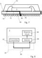
- the security track 86 forms part of a security mechanism 82 which reacts to a disruption of the security track.
- the security mechanism comprises the security track and connections between the security track and the integrated circuit 2 and circuitry 87, 88, 89 within the integrated circuit which monitors for an attack on the integrity of the security track.
- the security mechanism 82 does not generally interfere in the operation of the integrated circuit 2 unless and until it detects an attack on the integrity of the security track 86.
- the security mechanism 82 employs a transmitter 87 to direct a signal along the security track 86.
- This signal may be a voltage, a current or s dynamic signal such as a clock or digital stream of bits. Equally, it may be a DC or an AC voltage or current.
- a detection circuit 88 monitors for any change to the signal at the opposite end of the security track to the transmitter. The detection of a change to the signal by the detection circuit would result in counter measures by a response circuit 89 preventing the normal operation of the chip.
- the countermeasures may comprise resetting or disabling all or part of the functionalities of the chip. These counter measures may include disabling the functioning of the integrated circuit or erasing the contents of memory on the integrated circuit or both.
- a security track may be considered as a conductive track which is electrically connected, for example using a combination of tracks, vias and wire-bonds, to at least two terminals of the integrated circuit. This allows a first connection at one end of the security track to a first terminal and in turn to the transmitter of the security mechanism. The connection to a second terminal is provided at the opposite end of the security track. The second terminal in turn provides a connection to the detector of the security mechanism.
- the security mechanism may be a passive shield or an active shield. In both instances, a signal is provided by a signal transmitter to a first end of the conductive track and the detection circuit is employed to monitor the opposite end of conductive track.
- sequences of bits are injected at the start of the conductive track and subsequently tested at the other end by the detection circuit to check whether the sequence of bits arrive unaltered after their journey along the security track.
Landscapes
- Semiconductor Integrated Circuits (AREA)
- Physics & Mathematics (AREA)
- Health & Medical Sciences (AREA)
- Electromagnetism (AREA)
- Toxicology (AREA)
- Geometry (AREA)
Claims (8)
- Chip (40), umfassendein Substrat (8), das eine erste Oberfläche und eine zweite Oberfläche gegenüber der ersten Oberfläche aufweist;eine integrierte Schaltung (2), die auf einer Kontaktzone (42) auf der ersten Oberfläche des Substrats (8) montiert ist, wobei die Kontaktzone (42) eine Kontaktzonenregion des Substrats (8) definiert, die von einer Peripherieregion des Substrats (8) umgeben ist;eine Vielzahl von elektrischen Kontakten (16), die um die erste Oberfläche herum in der Peripherieregion bereitgestellt wird;eine Vielzahl von Drahtbindungen (74), die elektrische Anschlüsse zwischen der integrierten Schaltung (2) und der Vielzahl von elektrischen Kontakten (16) bereitstellen;eine Vielzahl von Lötperlenanschlüssen (80), die in der Peripherieregion auf der zweiten Oberfläche bereitgestellt wird;eine Vielzahl von Anschlüssen (15), die in dem Substrat (8) bereitgestellt wird, um die elektrischen Kontakte (16) auf der ersten Oberfläche an die Lötperlenanschlüsse (80) auf der zweiten Oberfläche anzuschließen;wobei das Substrat (8) mindestens eine Leiterbahn (72) umfasst, die über die Kontaktzonenregion (42) des Substrats (8) verlegt ist,wobei die mindestens eine Leiterbahn (72) einen elektrischen Anschluss an die integrierte Schaltung (4) bereitstellt, die zum normalen Betrieb der integrierten Schaltung (2) notwendig ist,dadurch gekennzeichnet, dass der Chip (4) derart konfiguriert ist, dass eine Abänderung der mindestens einen Leiterbahn den Betrieb der integrierten Schaltung (2) verhindert,wobei die mindestens eine Leiterbahn eine Sicherheitsbahn (86) ist, die Teil eines Sicherheitsmechanismus (82) ist, wobei der Sicherheitsmechanismus (82) dazu konfiguriert ist, eine Störung der Integrität der Sicherheitsbahn (86) zu detektieren und als Reaktion darauf mindestens eine Gegenmaßnahme einzuleiten, wobei der Sicherheitsmechanismus (82) umfasst:einen Signalsender (87) auf der integrierten Schaltung (2), um ein Signal an ein erstes Ende der Sicherheitsbahn (86) bereitzustellen; undeine Detektionsschaltung (88), die an ein zweites Ende der Sicherheitsbahn (86) angeschlossen ist, um eine Abänderung des Signals zu detektieren,wobei der Sicherheitsmechanismus (82) ferner eine Reaktionsschaltung (89) umfasst, die auf die Detektionsschaltung (88) reagiert, um die Ausführung der mindestens einen Gegenmaßnahme zu bewirken, und wobei die mindestens eine Gegenmaßnahme das Zurücksetzen oder Desaktivieren aller oder einiger der Funktionen des Chips umfasst.
- Chip nach Anspruch 1, wobei eine Massefläche (62) als eine Schicht aus einem leitfähigen Material in der Kontaktzonenregion (42) des Substrats bereitgestellt wird, und wobei die mindestens eine Bahn (72) einen isolierten Weg befolgt, der die Massefläche (62) partitioniert.
- Chip nach Anspruch 1, wobei eine Versorgungsfläche als eine Schicht aus leitfähigem Material in der Kontaktzonenregion (42) des Substrats (8) bereitgestellt wird, und die mindestens eine Bahn einen isolierten Weg befolgt, der die Versorgungsfläche partitioniert.
- Chip nach Anspruch 1, wobei die mindestens eine Leiterbahn (72) an mindestens eine Lötperle (80) elektrisch angeschlossen ist, wobei die mindestens eine Lötperle (80) in der Kontaktzonenregion (42) des Substrats (8) positioniert ist.
- Verfahren zum Schützen eines Chips mit Kugelgitteranordnung in einem Drahtbond-Gehäuse vor Abänderungen, umfassend folgende SchritteBilden eines Substrats, das eine erste Oberfläche und eine zweite Oberfläche gegenüber der ersten Oberfläche aufweist, die eine Kontaktzone für eine integrierte Schaltung aufweist, wobei die Kontaktzone eine Kontaktzonenregion des Substrats definiert, wobei das Bilden des Substrats das Bereitstellen einer Vielzahl von elektrischen Kontakten um die erste Oberfläche herum in einer Peripherieregion umfasst, wobei die Peripherieregion die Kontaktzonenregion umgibt;Montieren der integrierten Schaltung auf der Kontaktzone;Anschließen einer Vielzahl von Drahtbindungen zwischen der integrierten Schaltung und der Vielzahl von elektrischen Kontakten;Bereitstellen einer Vielzahl von Lötperlenanschlüssen auf einer Peripherieregion der zweiten Oberfläche;wobei der Schritt des Bildens des Substrats das Bereitstellen einer Vielzahl von Anschlüssen in dem Substrat zum Anschließen der elektrischen Kontakte auf der ersten Oberfläche an die Lötperlenanschlüsse auf der zweiten Oberfläche umfasst;wobei das Bilden des Substrats das Verlegen mindestens einer Leiterbahn über die Kontaktzonenregion des Substrats umfasst,wobei die mindestens eine Bahn einen elektrischen Anschluss an die integrierte Schaltung bereitstellt, der zum anschließenden richtigen Betrieb der integrierten Schaltung notwendig ist,dadurch gekennzeichnet, dass der Chip derart konfiguriert ist, dass eine Abänderung der mindestens einen Leiterbahn den Betrieb der integrierten Schaltung verhindert,wobei die mindestens eine Leiterbahn eine Sicherheitsbahn ist, wobei das Verfahren ferner umfasstBereitstellen eines Sicherheitsmechanismus, der die Sicherheitsbahn umfasst, wobei der Sicherheitsmechanismus dazu konfiguriert ist, eine Störung der Integrität der Sicherheitsbahn zu detektieren und als Reaktion darauf mindestens eine Gegenmaßnahme einzuleiten,Bereitstellen durch den Sicherheitsmechanismus eines Signals an einem ersten Ende der Sicherheitsbahn; undDetektieren einer Abänderung des Signals an einem zweiten Ende der Sicherheitsbahn und als Reaktion auf das Detektieren einer Abänderung, Bewirken der Ausführung der mindestens einen Gegenmaßnahme, und wobei die mindestens eine Gegenmaßnahme das Zurücksetzen oder Desaktivieren aller oder einiger der Funktionen des Chips umfasst.
- Verfahren nach Anspruch 5, wobei das Verfahren den Schritt des Bildens einer Schicht aus leitfähigem Material in der Kontaktzonenregion des Substrats umfasst, um als Massefläche zu dienen, wobei die mindestens eine Bahn einen isolierten Weg befolgt, der die Massefläche partitioniert.
- Verfahren nach Anspruch 6, ferner umfassend das Bereitstellen einer Schicht aus leitfähigem Material in der Kontaktzonenregion des Substrats, um als Versorgungsfläche zu dienen, und die mindestens eine Bahn einen isolierten Weg befolgt, der die Versorgungsfläche partitioniert.
- Verfahren nach Anspruch 6, ferner umfassend den Schritt des Bildens eines leitfähigen Wegs unter Verwendung der mindestens einen Leiterbahn zwischen einem der Kontakte der ersten Oberfläche und mindestens einer Lötperle, wobei die mindestens eine Lötperle in der Kontaktzonenregion des Substrats positioniert ist.
Applications Claiming Priority (2)
| Application Number | Priority Date | Filing Date | Title |
|---|---|---|---|
| EP18202853.0A EP3644351A1 (de) | 2018-10-26 | 2018-10-26 | Schutz von integrierten schaltungschips, die in einer drahtgebundenen kugelgitteranordnung gepackt sind |
| PCT/EP2019/078247 WO2020083745A1 (en) | 2018-10-26 | 2019-10-17 | Protection of wire-bond ball grid array packaged integrated circuit chips |
Publications (3)
| Publication Number | Publication Date |
|---|---|
| EP3871252A1 EP3871252A1 (de) | 2021-09-01 |
| EP3871252C0 EP3871252C0 (de) | 2025-03-12 |
| EP3871252B1 true EP3871252B1 (de) | 2025-03-12 |
Family
ID=64082885
Family Applications (2)
| Application Number | Title | Priority Date | Filing Date |
|---|---|---|---|
| EP18202853.0A Withdrawn EP3644351A1 (de) | 2018-10-26 | 2018-10-26 | Schutz von integrierten schaltungschips, die in einer drahtgebundenen kugelgitteranordnung gepackt sind |
| EP19786606.4A Active EP3871252B1 (de) | 2018-10-26 | 2019-10-17 | Schutz von integrierten schaltungschips, die in einer drahtgebundenen kugelgitteranordnung gepackt sind |
Family Applications Before (1)
| Application Number | Title | Priority Date | Filing Date |
|---|---|---|---|
| EP18202853.0A Withdrawn EP3644351A1 (de) | 2018-10-26 | 2018-10-26 | Schutz von integrierten schaltungschips, die in einer drahtgebundenen kugelgitteranordnung gepackt sind |
Country Status (8)
| Country | Link |
|---|---|
| US (1) | US12033925B2 (de) |
| EP (2) | EP3644351A1 (de) |
| JP (1) | JP7407811B2 (de) |
| KR (1) | KR102887056B1 (de) |
| CN (1) | CN112913004B (de) |
| ES (1) | ES3019233T3 (de) |
| SG (1) | SG11202102932SA (de) |
| WO (1) | WO2020083745A1 (de) |
Family Cites Families (11)
| Publication number | Priority date | Publication date | Assignee | Title |
|---|---|---|---|---|
| MY123146A (en) * | 1996-03-28 | 2006-05-31 | Intel Corp | Perimeter matrix ball grid array circuit package with a populated center |
| US7161239B2 (en) | 2000-12-22 | 2007-01-09 | Broadcom Corporation | Ball grid array package enhanced with a thermal and electrical connector |
| KR101166575B1 (ko) * | 2002-09-17 | 2012-07-18 | 스태츠 칩팩, 엘티디. | 적층형 패키지들 간 도선연결에 의한 상호연결을 이용한반도체 멀티-패키지 모듈 및 그 제작 방법 |
| US7528474B2 (en) * | 2005-05-31 | 2009-05-05 | Stats Chippac Ltd. | Stacked semiconductor package assembly having hollowed substrate |
| KR100849182B1 (ko) * | 2007-01-22 | 2008-07-30 | 삼성전자주식회사 | 반도체 카드 패키지 및 그 제조방법 |
| US7923830B2 (en) * | 2007-04-13 | 2011-04-12 | Maxim Integrated Products, Inc. | Package-on-package secure module having anti-tamper mesh in the substrate of the upper package |
| US7868441B2 (en) | 2007-04-13 | 2011-01-11 | Maxim Integrated Products, Inc. | Package on-package secure module having BGA mesh cap |
| KR101564070B1 (ko) * | 2009-05-01 | 2015-10-29 | 삼성전자주식회사 | 인쇄 회로 기판 및 이를 이용한 반도체 패키지 |
| US8910310B2 (en) * | 2012-05-17 | 2014-12-09 | Silicon Motion, Inc. | Embedded flash memory card and electronic device using the same, and engineering board for embedded flash memory card |
| JP6237982B2 (ja) | 2013-04-23 | 2017-11-29 | セイコーエプソン株式会社 | 物理量センサー、電子機器及び移動体 |
| WO2016180977A1 (en) * | 2015-05-13 | 2016-11-17 | Nagravision S.A. | Integrated circuit chip protection against physical and/or electrical alterations |
-
2018
- 2018-10-26 EP EP18202853.0A patent/EP3644351A1/de not_active Withdrawn
-
2019
- 2019-10-17 JP JP2021521841A patent/JP7407811B2/ja active Active
- 2019-10-17 EP EP19786606.4A patent/EP3871252B1/de active Active
- 2019-10-17 WO PCT/EP2019/078247 patent/WO2020083745A1/en not_active Ceased
- 2019-10-17 KR KR1020217012834A patent/KR102887056B1/ko active Active
- 2019-10-17 CN CN201980069250.1A patent/CN112913004B/zh active Active
- 2019-10-17 US US17/286,709 patent/US12033925B2/en active Active
- 2019-10-17 ES ES19786606T patent/ES3019233T3/es active Active
- 2019-10-17 SG SG11202102932SA patent/SG11202102932SA/en unknown
Also Published As
| Publication number | Publication date |
|---|---|
| SG11202102932SA (en) | 2021-04-29 |
| JP2022505555A (ja) | 2022-01-14 |
| JP7407811B2 (ja) | 2024-01-04 |
| EP3871252C0 (de) | 2025-03-12 |
| KR20210083272A (ko) | 2021-07-06 |
| ES3019233T3 (en) | 2025-05-20 |
| CN112913004B (zh) | 2025-06-17 |
| EP3871252A1 (de) | 2021-09-01 |
| EP3644351A1 (de) | 2020-04-29 |
| CN112913004A (zh) | 2021-06-04 |
| US20210358837A1 (en) | 2021-11-18 |
| WO2020083745A1 (en) | 2020-04-30 |
| KR102887056B1 (ko) | 2025-11-19 |
| US12033925B2 (en) | 2024-07-09 |
Similar Documents
| Publication | Publication Date | Title |
|---|---|---|
| CN101889344B (zh) | 嵌入式封装防篡改网栅 | |
| US7952478B2 (en) | Capacitance-based microchip exploitation detection | |
| US11502047B2 (en) | Packaging techniques for backside mesh connectivity | |
| JP6635276B2 (ja) | 攻撃検知機能を備える電子装置、その設計方法及びその製造方法 | |
| CN101593745A (zh) | 用于集成电路的封环结构 | |
| CN107787499B (zh) | 以防物理更改和/或电更改的集成电路芯片保护 | |
| US6020746A (en) | Method and apparatus for probing an integrated circuit through the back side of an integrated circuit die | |
| JP7495551B2 (ja) | 半導体装置 | |
| US12033925B2 (en) | Protection of wire-bond ball grid array packaged integrated circuit chips | |
| CN120850372A (zh) | 篡改检测技术 | |
| JP2870162B2 (ja) | 半導体装置およびその製造方法 | |
| US4959708A (en) | MOS integrated circuit with vertical shield | |
| JP4065876B2 (ja) | パッド下の集積半導体構造 | |
| US20030160294A1 (en) | Substrate for semiconductor package | |
| KR100382250B1 (ko) | 표면이 커버링된 반도체칩 | |
| US10473709B2 (en) | Integrated circuit chip stack | |
| US12614004B2 (en) | Detection of security attacks through die-attach pad | |
| US12632608B2 (en) | Integrated circuit device with protection against malicious attacks | |
| EP3937055A1 (de) | Integrierte schaltvorrichtung mit schutz gegen bösartige angriffe | |
| US11894315B2 (en) | Electronic system in package comprising protected side faces | |
| KR20050012950A (ko) | 스마트 카드 집적회로 칩 차폐용 메탈층을 이용한 접지방법 | |
| JPH0318744B2 (de) | ||
| HK1149365B (en) | Embedded package security tamper mesh |
Legal Events
| Date | Code | Title | Description |
|---|---|---|---|
| STAA | Information on the status of an ep patent application or granted ep patent |
Free format text: STATUS: UNKNOWN |
|
| STAA | Information on the status of an ep patent application or granted ep patent |
Free format text: STATUS: THE INTERNATIONAL PUBLICATION HAS BEEN MADE |
|
| PUAI | Public reference made under article 153(3) epc to a published international application that has entered the european phase |
Free format text: ORIGINAL CODE: 0009012 |
|
| STAA | Information on the status of an ep patent application or granted ep patent |
Free format text: STATUS: REQUEST FOR EXAMINATION WAS MADE |
|
| 17P | Request for examination filed |
Effective date: 20210412 |
|
| AK | Designated contracting states |
Kind code of ref document: A1 Designated state(s): AL AT BE BG CH CY CZ DE DK EE ES FI FR GB GR HR HU IE IS IT LI LT LU LV MC MK MT NL NO PL PT RO RS SE SI SK SM TR |
|
| DAV | Request for validation of the european patent (deleted) | ||
| DAX | Request for extension of the european patent (deleted) | ||
| RAP3 | Party data changed (applicant data changed or rights of an application transferred) |
Owner name: NAGRAVISION SARL |
|
| STAA | Information on the status of an ep patent application or granted ep patent |
Free format text: STATUS: EXAMINATION IS IN PROGRESS |
|
| 17Q | First examination report despatched |
Effective date: 20230809 |
|
| GRAP | Despatch of communication of intention to grant a patent |
Free format text: ORIGINAL CODE: EPIDOSNIGR1 |
|
| STAA | Information on the status of an ep patent application or granted ep patent |
Free format text: STATUS: GRANT OF PATENT IS INTENDED |
|
| INTG | Intention to grant announced |
Effective date: 20241009 |
|
| GRAS | Grant fee paid |
Free format text: ORIGINAL CODE: EPIDOSNIGR3 |
|
| GRAA | (expected) grant |
Free format text: ORIGINAL CODE: 0009210 |
|
| STAA | Information on the status of an ep patent application or granted ep patent |
Free format text: STATUS: THE PATENT HAS BEEN GRANTED |
|
| AK | Designated contracting states |
Kind code of ref document: B1 Designated state(s): AL AT BE BG CH CY CZ DE DK EE ES FI FR GB GR HR HU IE IS IT LI LT LU LV MC MK MT NL NO PL PT RO RS SE SI SK SM TR |
|
| REG | Reference to a national code |
Ref country code: GB Ref legal event code: FG4D |
|
| REG | Reference to a national code |
Ref country code: CH Ref legal event code: EP |
|
| REG | Reference to a national code |
Ref country code: DE Ref legal event code: R096 Ref document number: 602019067206 Country of ref document: DE |
|
| REG | Reference to a national code |
Ref country code: IE Ref legal event code: FG4D |
|
| U01 | Request for unitary effect filed |
Effective date: 20250327 |
|
| U07 | Unitary effect registered |
Designated state(s): AT BE BG DE DK EE FI FR IT LT LU LV MT NL PT RO SE SI Effective date: 20250403 |
|
| REG | Reference to a national code |
Ref country code: ES Ref legal event code: FG2A Ref document number: 3019233 Country of ref document: ES Kind code of ref document: T3 Effective date: 20250520 |
|
| PG25 | Lapsed in a contracting state [announced via postgrant information from national office to epo] |
Ref country code: RS Free format text: LAPSE BECAUSE OF FAILURE TO SUBMIT A TRANSLATION OF THE DESCRIPTION OR TO PAY THE FEE WITHIN THE PRESCRIBED TIME-LIMIT Effective date: 20250612 |
|
| PG25 | Lapsed in a contracting state [announced via postgrant information from national office to epo] |
Ref country code: NO Free format text: LAPSE BECAUSE OF FAILURE TO SUBMIT A TRANSLATION OF THE DESCRIPTION OR TO PAY THE FEE WITHIN THE PRESCRIBED TIME-LIMIT Effective date: 20250612 |
|
| PG25 | Lapsed in a contracting state [announced via postgrant information from national office to epo] |
Ref country code: HR Free format text: LAPSE BECAUSE OF FAILURE TO SUBMIT A TRANSLATION OF THE DESCRIPTION OR TO PAY THE FEE WITHIN THE PRESCRIBED TIME-LIMIT Effective date: 20250312 |
|
| PG25 | Lapsed in a contracting state [announced via postgrant information from national office to epo] |
Ref country code: GR Free format text: LAPSE BECAUSE OF FAILURE TO SUBMIT A TRANSLATION OF THE DESCRIPTION OR TO PAY THE FEE WITHIN THE PRESCRIBED TIME-LIMIT Effective date: 20250613 |
|
| PG25 | Lapsed in a contracting state [announced via postgrant information from national office to epo] |
Ref country code: SM Free format text: LAPSE BECAUSE OF FAILURE TO SUBMIT A TRANSLATION OF THE DESCRIPTION OR TO PAY THE FEE WITHIN THE PRESCRIBED TIME-LIMIT Effective date: 20250312 |
|
| PG25 | Lapsed in a contracting state [announced via postgrant information from national office to epo] |
Ref country code: PL Free format text: LAPSE BECAUSE OF FAILURE TO SUBMIT A TRANSLATION OF THE DESCRIPTION OR TO PAY THE FEE WITHIN THE PRESCRIBED TIME-LIMIT Effective date: 20250312 |
|
| PGFP | Annual fee paid to national office [announced via postgrant information from national office to epo] |
Ref country code: GB Payment date: 20250923 Year of fee payment: 7 |
|
| PG25 | Lapsed in a contracting state [announced via postgrant information from national office to epo] |
Ref country code: CZ Free format text: LAPSE BECAUSE OF FAILURE TO SUBMIT A TRANSLATION OF THE DESCRIPTION OR TO PAY THE FEE WITHIN THE PRESCRIBED TIME-LIMIT Effective date: 20250312 |
|
| PG25 | Lapsed in a contracting state [announced via postgrant information from national office to epo] |
Ref country code: SK Free format text: LAPSE BECAUSE OF FAILURE TO SUBMIT A TRANSLATION OF THE DESCRIPTION OR TO PAY THE FEE WITHIN THE PRESCRIBED TIME-LIMIT Effective date: 20250312 |
|
| PG25 | Lapsed in a contracting state [announced via postgrant information from national office to epo] |
Ref country code: IS Free format text: LAPSE BECAUSE OF FAILURE TO SUBMIT A TRANSLATION OF THE DESCRIPTION OR TO PAY THE FEE WITHIN THE PRESCRIBED TIME-LIMIT Effective date: 20250712 |
|
| U20 | Renewal fee for the european patent with unitary effect paid |
Year of fee payment: 7 Effective date: 20250923 |
|
| PLBE | No opposition filed within time limit |
Free format text: ORIGINAL CODE: 0009261 |
|
| STAA | Information on the status of an ep patent application or granted ep patent |
Free format text: STATUS: NO OPPOSITION FILED WITHIN TIME LIMIT |
|
| REG | Reference to a national code |
Ref country code: CH Ref legal event code: L10 Free format text: ST27 STATUS EVENT CODE: U-0-0-L10-L00 (AS PROVIDED BY THE NATIONAL OFFICE) Effective date: 20260121 |
|
| PGFP | Annual fee paid to national office [announced via postgrant information from national office to epo] |
Ref country code: ES Payment date: 20251103 Year of fee payment: 7 |
|
| 26N | No opposition filed |
Effective date: 20251215 |