EP3866572B1 - Methods for producing a metallic pattern on a substrate - Google Patents
Methods for producing a metallic pattern on a substrate Download PDFInfo
- Publication number
- EP3866572B1 EP3866572B1 EP21166748.0A EP21166748A EP3866572B1 EP 3866572 B1 EP3866572 B1 EP 3866572B1 EP 21166748 A EP21166748 A EP 21166748A EP 3866572 B1 EP3866572 B1 EP 3866572B1
- Authority
- EP
- European Patent Office
- Prior art keywords
- metallic
- ink
- copper
- resist
- etch
- Prior art date
- Legal status (The legal status is an assumption and is not a legal conclusion. Google has not performed a legal analysis and makes no representation as to the accuracy of the status listed.)
- Active
Links
Images
Classifications
-
- G—PHYSICS
- G03—PHOTOGRAPHY; CINEMATOGRAPHY; ANALOGOUS TECHNIQUES USING WAVES OTHER THAN OPTICAL WAVES; ELECTROGRAPHY; HOLOGRAPHY
- G03F—PHOTOMECHANICAL PRODUCTION OF TEXTURED OR PATTERNED SURFACES, e.g. FOR PRINTING, FOR PROCESSING OF SEMICONDUCTOR DEVICES; MATERIALS THEREFOR; ORIGINALS THEREFOR; APPARATUS SPECIALLY ADAPTED THEREFOR
- G03F1/00—Originals for photomechanical production of textured or patterned surfaces, e.g., masks, photo-masks, reticles; Mask blanks or pellicles therefor; Containers specially adapted therefor; Preparation thereof
- G03F1/92—Originals for photomechanical production of textured or patterned surfaces, e.g., masks, photo-masks, reticles; Mask blanks or pellicles therefor; Containers specially adapted therefor; Preparation thereof prepared from printing surfaces
-
- C—CHEMISTRY; METALLURGY
- C23—COATING METALLIC MATERIAL; COATING MATERIAL WITH METALLIC MATERIAL; CHEMICAL SURFACE TREATMENT; DIFFUSION TREATMENT OF METALLIC MATERIAL; COATING BY VACUUM EVAPORATION, BY SPUTTERING, BY ION IMPLANTATION OR BY CHEMICAL VAPOUR DEPOSITION, IN GENERAL; INHIBITING CORROSION OF METALLIC MATERIAL OR INCRUSTATION IN GENERAL
- C23F—NON-MECHANICAL REMOVAL OF METALLIC MATERIAL FROM SURFACE; INHIBITING CORROSION OF METALLIC MATERIAL OR INCRUSTATION IN GENERAL; MULTI-STEP PROCESSES FOR SURFACE TREATMENT OF METALLIC MATERIAL INVOLVING AT LEAST ONE PROCESS PROVIDED FOR IN CLASS C23 AND AT LEAST ONE PROCESS COVERED BY SUBCLASS C21D OR C22F OR CLASS C25
- C23F1/00—Etching metallic material by chemical means
- C23F1/02—Local etching
-
- H—ELECTRICITY
- H05—ELECTRIC TECHNIQUES NOT OTHERWISE PROVIDED FOR
- H05K—PRINTED CIRCUITS; CASINGS OR CONSTRUCTIONAL DETAILS OF ELECTRIC APPARATUS; MANUFACTURE OF ASSEMBLAGES OF ELECTRICAL COMPONENTS
- H05K3/00—Apparatus or processes for manufacturing printed circuits
- H05K3/02—Apparatus or processes for manufacturing printed circuits in which the conductive material is applied to the surface of the insulating support and is thereafter removed from such areas of the surface which are not intended for current conducting or shielding
- H05K3/06—Apparatus or processes for manufacturing printed circuits in which the conductive material is applied to the surface of the insulating support and is thereafter removed from such areas of the surface which are not intended for current conducting or shielding the conductive material being removed chemically or electrolytically, e.g. by photo-etch process
- H05K3/061—Etching masks
-
- B—PERFORMING OPERATIONS; TRANSPORTING
- B41—PRINTING; LINING MACHINES; TYPEWRITERS; STAMPS
- B41M—PRINTING, DUPLICATING, MARKING, OR COPYING PROCESSES; COLOUR PRINTING
- B41M5/00—Duplicating or marking methods; Sheet materials for use therein
- B41M5/0041—Digital printing on surfaces other than ordinary paper
- B41M5/0058—Digital printing on surfaces other than ordinary paper on metals and oxidised metal surfaces
-
- C—CHEMISTRY; METALLURGY
- C09—DYES; PAINTS; POLISHES; NATURAL RESINS; ADHESIVES; COMPOSITIONS NOT OTHERWISE PROVIDED FOR; APPLICATIONS OF MATERIALS NOT OTHERWISE PROVIDED FOR
- C09D—COATING COMPOSITIONS, e.g. PAINTS, VARNISHES OR LACQUERS; FILLING PASTES; CHEMICAL PAINT OR INK REMOVERS; INKS; CORRECTING FLUIDS; WOODSTAINS; PASTES OR SOLIDS FOR COLOURING OR PRINTING; USE OF MATERIALS THEREFOR
- C09D11/00—Inks
- C09D11/02—Printing inks
- C09D11/10—Printing inks based on artificial resins
- C09D11/101—Inks specially adapted for printing processes involving curing by wave energy or particle radiation, e.g. with UV-curing following the printing
-
- C—CHEMISTRY; METALLURGY
- C09—DYES; PAINTS; POLISHES; NATURAL RESINS; ADHESIVES; COMPOSITIONS NOT OTHERWISE PROVIDED FOR; APPLICATIONS OF MATERIALS NOT OTHERWISE PROVIDED FOR
- C09D—COATING COMPOSITIONS, e.g. PAINTS, VARNISHES OR LACQUERS; FILLING PASTES; CHEMICAL PAINT OR INK REMOVERS; INKS; CORRECTING FLUIDS; WOODSTAINS; PASTES OR SOLIDS FOR COLOURING OR PRINTING; USE OF MATERIALS THEREFOR
- C09D11/00—Inks
- C09D11/30—Inkjet printing inks
-
- C—CHEMISTRY; METALLURGY
- C23—COATING METALLIC MATERIAL; COATING MATERIAL WITH METALLIC MATERIAL; CHEMICAL SURFACE TREATMENT; DIFFUSION TREATMENT OF METALLIC MATERIAL; COATING BY VACUUM EVAPORATION, BY SPUTTERING, BY ION IMPLANTATION OR BY CHEMICAL VAPOUR DEPOSITION, IN GENERAL; INHIBITING CORROSION OF METALLIC MATERIAL OR INCRUSTATION IN GENERAL
- C23F—NON-MECHANICAL REMOVAL OF METALLIC MATERIAL FROM SURFACE; INHIBITING CORROSION OF METALLIC MATERIAL OR INCRUSTATION IN GENERAL; MULTI-STEP PROCESSES FOR SURFACE TREATMENT OF METALLIC MATERIAL INVOLVING AT LEAST ONE PROCESS PROVIDED FOR IN CLASS C23 AND AT LEAST ONE PROCESS COVERED BY SUBCLASS C21D OR C22F OR CLASS C25
- C23F1/00—Etching metallic material by chemical means
-
- G—PHYSICS
- G03—PHOTOGRAPHY; CINEMATOGRAPHY; ANALOGOUS TECHNIQUES USING WAVES OTHER THAN OPTICAL WAVES; ELECTROGRAPHY; HOLOGRAPHY
- G03F—PHOTOMECHANICAL PRODUCTION OF TEXTURED OR PATTERNED SURFACES, e.g. FOR PRINTING, FOR PROCESSING OF SEMICONDUCTOR DEVICES; MATERIALS THEREFOR; ORIGINALS THEREFOR; APPARATUS SPECIALLY ADAPTED THEREFOR
- G03F1/00—Originals for photomechanical production of textured or patterned surfaces, e.g., masks, photo-masks, reticles; Mask blanks or pellicles therefor; Containers specially adapted therefor; Preparation thereof
- G03F1/50—Mask blanks not covered by G03F1/20 - G03F1/34; Preparation thereof
-
- G—PHYSICS
- G03—PHOTOGRAPHY; CINEMATOGRAPHY; ANALOGOUS TECHNIQUES USING WAVES OTHER THAN OPTICAL WAVES; ELECTROGRAPHY; HOLOGRAPHY
- G03F—PHOTOMECHANICAL PRODUCTION OF TEXTURED OR PATTERNED SURFACES, e.g. FOR PRINTING, FOR PROCESSING OF SEMICONDUCTOR DEVICES; MATERIALS THEREFOR; ORIGINALS THEREFOR; APPARATUS SPECIALLY ADAPTED THEREFOR
- G03F7/00—Photomechanical, e.g. photolithographic, production of textured or patterned surfaces, e.g. printing surfaces; Materials therefor, e.g. comprising photoresists; Apparatus specially adapted therefor
- G03F7/20—Exposure; Apparatus therefor
- G03F7/2002—Exposure; Apparatus therefor with visible light or UV light, through an original having an opaque pattern on a transparent support, e.g. film printing, projection printing; by reflection of visible or UV light from an original such as a printed image
- G03F7/2014—Contact or film exposure of light sensitive plates such as lithographic plates or circuit boards, e.g. in a vacuum frame
- G03F7/2016—Contact mask being integral part of the photosensitive element and subject to destructive removal during post-exposure processing
- G03F7/2018—Masking pattern obtained by selective application of an ink or a toner, e.g. ink jet printing
-
- H—ELECTRICITY
- H05—ELECTRIC TECHNIQUES NOT OTHERWISE PROVIDED FOR
- H05K—PRINTED CIRCUITS; CASINGS OR CONSTRUCTIONAL DETAILS OF ELECTRIC APPARATUS; MANUFACTURE OF ASSEMBLAGES OF ELECTRICAL COMPONENTS
- H05K3/00—Apparatus or processes for manufacturing printed circuits
- H05K3/0002—Apparatus or processes for manufacturing printed circuits for manufacturing artworks for printed circuits
-
- H—ELECTRICITY
- H05—ELECTRIC TECHNIQUES NOT OTHERWISE PROVIDED FOR
- H05K—PRINTED CIRCUITS; CASINGS OR CONSTRUCTIONAL DETAILS OF ELECTRIC APPARATUS; MANUFACTURE OF ASSEMBLAGES OF ELECTRICAL COMPONENTS
- H05K3/00—Apparatus or processes for manufacturing printed circuits
- H05K3/0011—Working of insulating substrates or insulating layers
- H05K3/0017—Etching of the substrate by chemical or physical means
-
- H—ELECTRICITY
- H05—ELECTRIC TECHNIQUES NOT OTHERWISE PROVIDED FOR
- H05K—PRINTED CIRCUITS; CASINGS OR CONSTRUCTIONAL DETAILS OF ELECTRIC APPARATUS; MANUFACTURE OF ASSEMBLAGES OF ELECTRICAL COMPONENTS
- H05K3/00—Apparatus or processes for manufacturing printed circuits
- H05K3/0073—Masks not provided for in groups H05K3/02 - H05K3/46, e.g. for photomechanical production of patterned surfaces
- H05K3/0079—Masks not provided for in groups H05K3/02 - H05K3/46, e.g. for photomechanical production of patterned surfaces characterised by the method of application or removal of the mask
-
- H—ELECTRICITY
- H10—SEMICONDUCTOR DEVICES; ELECTRIC SOLID-STATE DEVICES NOT OTHERWISE PROVIDED FOR
- H10K—ORGANIC ELECTRIC SOLID-STATE DEVICES
- H10K71/00—Manufacture or treatment specially adapted for the organic devices covered by this subclass
- H10K71/10—Deposition of organic active material
- H10K71/12—Deposition of organic active material using liquid deposition, e.g. spin coating
- H10K71/13—Deposition of organic active material using liquid deposition, e.g. spin coating using printing techniques, e.g. ink-jet printing or screen printing
- H10K71/135—Deposition of organic active material using liquid deposition, e.g. spin coating using printing techniques, e.g. ink-jet printing or screen printing using ink-jet printing
-
- H—ELECTRICITY
- H05—ELECTRIC TECHNIQUES NOT OTHERWISE PROVIDED FOR
- H05K—PRINTED CIRCUITS; CASINGS OR CONSTRUCTIONAL DETAILS OF ELECTRIC APPARATUS; MANUFACTURE OF ASSEMBLAGES OF ELECTRICAL COMPONENTS
- H05K2203/00—Indexing scheme relating to apparatus or processes for manufacturing printed circuits covered by H05K3/00
- H05K2203/01—Tools for processing; Objects used during processing
- H05K2203/0104—Tools for processing; Objects used during processing for patterning or coating
- H05K2203/013—Inkjet printing, e.g. for printing insulating material or resist
-
- H—ELECTRICITY
- H05—ELECTRIC TECHNIQUES NOT OTHERWISE PROVIDED FOR
- H05K—PRINTED CIRCUITS; CASINGS OR CONSTRUCTIONAL DETAILS OF ELECTRIC APPARATUS; MANUFACTURE OF ASSEMBLAGES OF ELECTRICAL COMPONENTS
- H05K2203/00—Indexing scheme relating to apparatus or processes for manufacturing printed circuits covered by H05K3/00
- H05K2203/03—Metal processing
- H05K2203/0392—Pretreatment of metal, e.g. before finish plating, etching
-
- H—ELECTRICITY
- H05—ELECTRIC TECHNIQUES NOT OTHERWISE PROVIDED FOR
- H05K—PRINTED CIRCUITS; CASINGS OR CONSTRUCTIONAL DETAILS OF ELECTRIC APPARATUS; MANUFACTURE OF ASSEMBLAGES OF ELECTRICAL COMPONENTS
- H05K2203/00—Indexing scheme relating to apparatus or processes for manufacturing printed circuits covered by H05K3/00
- H05K2203/05—Patterning and lithography; Masks; Details of resist
- H05K2203/0562—Details of resist
- H05K2203/0582—Coating by resist, i.e. resist used as mask for application of insulating coating or of second resist
-
- H—ELECTRICITY
- H05—ELECTRIC TECHNIQUES NOT OTHERWISE PROVIDED FOR
- H05K—PRINTED CIRCUITS; CASINGS OR CONSTRUCTIONAL DETAILS OF ELECTRIC APPARATUS; MANUFACTURE OF ASSEMBLAGES OF ELECTRICAL COMPONENTS
- H05K2203/00—Indexing scheme relating to apparatus or processes for manufacturing printed circuits covered by H05K3/00
- H05K2203/11—Treatments characterised by their effect, e.g. heating, cooling, roughening
- H05K2203/1173—Differences in wettability, e.g. hydrophilic or hydrophobic areas
Definitions
- Embodiments of the invention relates to manufacturing of printed circuit boards by applying the etch-resist mask using non-impact printing such as, inkjet printing.
- PCBs Printed circuit boards
- the manufacturing of PCBs is considered cheaper, faster and more accurate than using other wiring methods such as point-to-point construction.
- the patterning of copper lines in the manufacturing process of a PCB is usually done by applying an etch-resist photo-mask on a copper layer laminated to an insulating material board and removing exposed copper portions by an etching process, leaving only the desired copper lines (also refer to as image patterning) as the electrically conducting paths.
- the etch-resist pattern can be applied on top of the copper layer by additive methods, for example by non-impact printing (e.g. inkjet printing) on top of the copper layer.
- non-impact printing e.g. inkjet printing
- Conventional inkjet materials have relatively low viscosity and accordingly when ink drops would hit a non-absorbing surface, such as a copper surface, uncontrolled spreading of the drops and other phenomena such as clustering, coalescence and extensive dot gain usually occur. Accordingly, the printed pattern, which is formed by inkjet printing technology, may exhibit poor quality or the copper lines including, for example, lack of details, inconsistent line width, poor line edge smoothness, shorts between adjacent lines and dis
- US 2006/060563 A1 discloses an aqueous ink composition for use in PCB for forming etching resist pattern and micro-channel, comprising aqueous polymer or polymer emulsion (in dry state), and water.
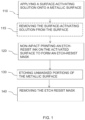
- the solution is defined in the independent method claim 1, a method of forming a metallic pattern on a substrate.
- the embodiments are defined in the dependent claims.
- Embodiments of the invention are related to methods of forming or applying an etch-resist mask on a metallic layer by non-impact printing, for example, during the manufacturing of printed circuit boards (PCBs).
- a method of applying an etch-resist mask on a metallic surface may include applying a chemically surface-activating solution on top of a metallic surface to chemically activate the metallic surface, followed by removing/washing the chemically activating solution from the surface and printing (e.g. inkjet printing) an etch resist ink on top of the activated surface.
- a reactive component of the etch-resist ink undergoes a chemical reaction with the activated surface to immobilize droplets of the liquid composition when hitting the surface.
- the chemical reaction may cause a significant increase in the ink droplet viscosity (for example, by one or two orders of magnitudes) instantaneously upon hitting the activated surface.
- the reactive component in the etch-resist ink may be an etch resist component and in other embodiments the reactive component may be different from the etch-resist component. According to some embodiments, more than one reactive component of the etch resist-ink may undergo a chemical reaction with components on the activated surface.
- the metallic layer may be a copper layer laminated onto an insulating nonconductive substrate.
- the description below refers to a copper surface. It should be realized that other metallic surfaces, such as, aluminum surfaces, stainless steel surfaces, gold surfaces and others are likewise applicable to embodiments of the invention.
- the method may include applying a chemically surface-activating solution onto a metallic surface, on which an etch-resist pattern is to be printed.
- the chemically surface-activating solution may be or may include any etching solution capable to chemically activate the surface.
- a chemically activated surface may be defined as a surface which, prior to the surface activation, will not react with the etch resist ink materials while it does react post the surface activation to cause the immobilization of the etch resist ink droplet.
- the surface-activating solution may include, for example, copper salts, ferric salts, chromic-sulfuric acids, persulfate salts, sodium chlorite and hydrogen peroxide.
- applying a chemically activating solution may include immersing the surface in a bath containing the chemically surface-activating solution, spraying the chemically surface-activating solution over the surface and any other suitable method.
- the method may include subjecting the metallic surface to the chemically activating solution (e.g., by immersing, spraying or the like) for a predetermined amount of time, for example, for 10 seconds, 20 seconds, 30 seconds, 60 seconds or more.
- the method may include optionally, removing the chemically surface-activating solution using, for example, an alcoholic solution.
- the method may include removing residues of the chemically surface-activating solution from the surface using ethanol.
- removing the chemically activating solution from the surface may be done using liquids other than alcoholic solutions, for example; propyl alcohol; iso-propyl alcohol; acetone.
- the method may include non-impact printing (e.g., by inkjet printing) an etch-resist ink onto the activated surface to produce an etch resist mask according to a predetermined pattern.
- the etch resist ink may comprise an etch-resist polymeric component that undergoes a chemical reaction with the activated surface to immobilize droplets of the etch-resist ink when hitting the activated surface.
- another ink component, different from the etch-resist component undergoes a chemical reaction with the activated surface to immobilize droplets of the etch-resist ink when hitting the activated surface.
- Non-limiting examples of etch resist polymeric reactive components may be acrylates, styrene acrylates, phosphates and sulfonates polymers, obtaining molecular weight (Mw) form 1000-17,000.
- the etch resist reactive polymeric component may be water-soluble and may include reactive anionic components.
- anionic etch-resist reactive component may include at least one anionic polymer (in a base form) at pH higher than 7.0.
- the anionic polymer may be selected from acrylic resins and styrene-acrylic resins in their dissolved salt forms, sulphonic resins in their dissolved salt form, such as sodium, ammonium or amine neutralized form or the like. Without wishing to be bound by any specific theoretical mechanism, the aforementioned resins may undergo a reaction with the reactive (activated) surface.
- the copper metal surface is activated to form copper cations on top of the copper and when an acrylic polymer (being in the etch-resist ink) would hit the surface, the anionic acrylate may react with the copper ions to form a polymeric matrix in the droplet, which would dramatically increase the droplet viscosity.
- the ink component that undergoes the chemical reaction with a surface-activated component to immobilize droplets of the etch-resist ink when hitting the activated surface may be different from the etch-resist component.
- the masked copper board may further be etched by a metal etching (e.g., acidic copper etching) solution to remove exposed, unmasked portions of the metallic layer.
- a metal etching e.g., acidic copper etching
- the etch resist mask may then be removed to expose a line pattern on the substrate, i.e., an insulating board.
- exemplary liquid compositions (etch-resist ink compositions as described herein) were printed on an FR4 copper clad board having a copper thickness of 18 micrometers.
- the copper was first chemically activated by applying a chemically surface-activating solution to activate the copper surface.
- a liquid composition of an etch resist ink was selectively printed according to a predetermined pattern on top of either the activated or inactivated copper surface, using ink-jet printing technology.
- % (w/w) is a measure of the concentration of a substance in terms of the percentage by weight relative to the weight of the composition.
- Copper from the unmasked exposed zones was etched away using an etchant bath containing a ferric chloride etchant solution of strength 42° Baume supplied by Amza (PERMIX 166).
- the etching was performed in a Spray Developer S31, supplied by Walter Lemmen GMBH, at a temperature of 35° C for 3 minutes.
- the etch resist mask was stripped off by immersing the etched board in a 1% (w/w) aqueous solution of NaOH at a temperature of 25° C followed by washing the FR4 copper board with water and drying by air at 25° C.
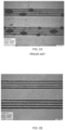
- Example 1 An etch resist ink, which is in a form of a liquid composition at room temperature, was printed on top of an untreated (inactivated) copper FR4 board.
- the liquid composition was prepared with 10% propylene glycol (as a humectant) and 1% (w/w) 2-Amino-2-methyl propanol, 0.3% (w/w) of BYK 348 supplied by BYK and 2 % (w/w) of Bayscript BA Cyan. These materials were dissolved in water containing 24% Joncryl 8085 styrene acrylic resin solution.
- the etch resist composition was printed on top of an FR4 copper clad board having a copper thickness of 18 micron, to produce the etch resist mask.
- the etch-resist mask was visually inspected. As can be shown in Fig. 2A , the printed pattern demonstrated very poor print quality with extremely poor edge definitions and severe shorts between the lines.
- Example 2 The liquid composition was prepared as detailed in Example 1.
- FR4 copper clad board surface was activated by dipping (e.g., immersing) the copper clad into an aqueous solution of CuCl 2 0.5% (w/w) for 30 seconds followed by washing the copper board with technical ethanol.
- the liquid composition was printed on top of the treated copper board and dried at 80° C to produce an insoluble etch resist mask.
- the etch resist pattern demonstrated a high print quality well-defined and thin lines width down to 50 micrometers contained sharp edges and no line breaks as can be shown in Fig. 2B .
- Etching of the exposed copper and removal of the etch resist mask were conducted as detailed in Example 1.
- the wiring pattern on the board demonstrated well-defined thin lines with a width down to 50 micrometers containing sharp edges and no line breaks.
- Example 3 The liquid composition was prepared as detailed in Example 1. The copper surface was activated by dipping the FR4 copper clad board into a bath containing 20% aqueous solution of FeCl 3 (w/w) for 10 sec following by washing the copper board with technical ethanol.
- Example 2 the liquid composition was inkjet-printed on the coated copper board and dried at 80° C to produce an insoluble etch resist mask.
- the etch resist pattern demonstrated a high print quality well-defined and thin lines down to 50 micrometers contained sharp edges and no line breaks.
- Etching of the exposed copper and removal of the etch resist mask were conducted as detailed in Example 1.
- the wiring pattern on the board demonstrated well-defined pattern with thin lines having a width of down to 30 micrometers sharp edges and no line breaks.
- Example 4 The liquid composition was prepared as detailed in Example 1. The copper surface was activated by dipping the FR4 copper clad board into an aqueous solution of Na 2 S 2 O 8 1% (w/w) for 30 sec following by washing the copper board with technical ethanol.
- the etch resist liquid composition was printed on the treated copper board and dried at 80° C to produce an insoluble etch resist mask.
- the etch resist pattern demonstrated a high print quality well-defined and thin lines down to 50 micrometers, contained sharp edges and no line breaks.
- the etching of the unmasked copper and removal of the etch resist mask were conducted as detailed in example 1.
- the wiring pattern produced by the etching and stripping processes demonstrated a well-defined pattern with thin lines having a width of down to 30 micrometers sharp edges and no line breaks.
- Table 1 below lists some non-limiting examples of chemically surface-activating components used in embodiments of the invention, their relative weigh concentrations in the surface-activating solution and suggested immersing time according to some embodiments of the invention.
- Table 1 Activating agent Concentration (w/w%) immersing time (Seconds) CuCl 2 (or any divalent copper salts) 0.5-1 30 Na 2 S 2 O 8 (or any persulfate salt) 0.5-1 30 H 2 O 2 10 30 FeCl 3 20 10 HCrO 4 /H 2 SO 4 5 30 NaClO 2 5 60
- etch-resist inks Table 2 below lists some non-limiting examples of etch-resist inks.
- Table 2 Etch-resist ink Etch-resist component 1 2 % (w/w) of Cyan dye, 10% propylene glycol, 1% (w/w) 2-Amino-2-methyl propanol and 0.3% (w/w) of surfactant were dissolved in water containing 24% styrene acrylic resin solution.
- Phosphates polymers Mw 500-17,000 3 2 % (w/w) of Cyan dye, 10% propylene glycol, 1% (w/w) 2-Amino-2-methyl propanol and 0.3% (w/w) of surfactant were dissolved in water containing 24% sulfonates resin solution. Sulfonates polymers Mw: 500-17,000
Landscapes
- Engineering & Computer Science (AREA)
- Manufacturing & Machinery (AREA)
- Chemical & Material Sciences (AREA)
- Microelectronics & Electronic Packaging (AREA)
- Materials Engineering (AREA)
- Organic Chemistry (AREA)
- General Physics & Mathematics (AREA)
- Physics & Mathematics (AREA)
- Life Sciences & Earth Sciences (AREA)
- Wood Science & Technology (AREA)
- Chemical Kinetics & Catalysis (AREA)
- General Chemical & Material Sciences (AREA)
- Mechanical Engineering (AREA)
- Metallurgy (AREA)
- ing And Chemical Polishing (AREA)
- Manufacturing Of Printed Circuit Boards (AREA)
- Weting (AREA)
Applications Claiming Priority (3)
| Application Number | Priority Date | Filing Date | Title |
|---|---|---|---|
| US201562204508P | 2015-08-13 | 2015-08-13 | |
| PCT/IL2016/050820 WO2017025949A1 (en) | 2015-08-13 | 2016-07-27 | Methods for producing an etch resist pattern on a metallic surface |
| EP16834759.9A EP3335079B1 (en) | 2015-08-13 | 2016-07-27 | Methods for producing an etch resist pattern on a metallic surface |
Related Parent Applications (2)
| Application Number | Title | Priority Date | Filing Date |
|---|---|---|---|
| EP16834759.9A Division EP3335079B1 (en) | 2015-08-13 | 2016-07-27 | Methods for producing an etch resist pattern on a metallic surface |
| EP16834759.9A Division-Into EP3335079B1 (en) | 2015-08-13 | 2016-07-27 | Methods for producing an etch resist pattern on a metallic surface |
Publications (3)
| Publication Number | Publication Date |
|---|---|
| EP3866572A2 EP3866572A2 (en) | 2021-08-18 |
| EP3866572A3 EP3866572A3 (en) | 2021-09-29 |
| EP3866572B1 true EP3866572B1 (en) | 2024-01-03 |
Family
ID=57983031
Family Applications (2)
| Application Number | Title | Priority Date | Filing Date |
|---|---|---|---|
| EP21166748.0A Active EP3866572B1 (en) | 2015-08-13 | 2016-07-27 | Methods for producing a metallic pattern on a substrate |
| EP16834759.9A Active EP3335079B1 (en) | 2015-08-13 | 2016-07-27 | Methods for producing an etch resist pattern on a metallic surface |
Family Applications After (1)
| Application Number | Title | Priority Date | Filing Date |
|---|---|---|---|
| EP16834759.9A Active EP3335079B1 (en) | 2015-08-13 | 2016-07-27 | Methods for producing an etch resist pattern on a metallic surface |
Country Status (6)
| Country | Link |
|---|---|
| US (5) | US10806035B2 (enExample) |
| EP (2) | EP3866572B1 (enExample) |
| JP (4) | JP6975463B2 (enExample) |
| KR (4) | KR102626521B1 (enExample) |
| CN (2) | CN114397795A (enExample) |
| WO (1) | WO2017025949A1 (enExample) |
Families Citing this family (9)
| Publication number | Priority date | Publication date | Assignee | Title |
|---|---|---|---|---|
| EP3304197A4 (en) | 2015-06-04 | 2019-01-23 | Kateeva, Inc. | METHOD FOR PRODUCING AN ESTETRESIST PATTERN ON A METALLIC SURFACE |
| KR102626521B1 (ko) * | 2015-08-13 | 2024-01-17 | 카티바, 인크. | 금속 표면 상에 에치 레지스트 패턴을 형성하는 방법 |
| US10398034B2 (en) * | 2016-12-12 | 2019-08-27 | Kateeva, Inc. | Methods of etching conductive features, and related devices and systems |
| US20200325583A1 (en) * | 2017-10-23 | 2020-10-15 | Mec Company., Ltd. | Method for Producing Film Formation Substrate, Film Formation Substrate, and Surface Treatment Agent |
| GB2583778B (en) * | 2019-03-29 | 2023-05-24 | Pierce Protocols Ltd | Glass etching preparation method and system |
| WO2020250784A1 (ja) * | 2019-06-11 | 2020-12-17 | 三菱瓦斯化学株式会社 | 水性組成物、これを用いたステンレス鋼表面の粗化処理方法、ならびに粗化処理されたステンレス鋼およびその製造方法 |
| CN110468413A (zh) * | 2019-09-10 | 2019-11-19 | 四会富仕电子科技股份有限公司 | 一种金属基表面粗化的方法 |
| CA3191956C (en) * | 2022-03-07 | 2025-11-18 | Catmarks Mfg Llc | Automotive part identification marking system |
| US12371797B2 (en) * | 2023-03-24 | 2025-07-29 | Adrienne Reisinger | Etching a design on a metal surface covered with a pigmented layer |
Family Cites Families (75)
| Publication number | Priority date | Publication date | Assignee | Title |
|---|---|---|---|---|
| GB1085860A (en) * | 1965-02-18 | 1967-10-04 | Fuji Photo Film Co Ltd | Method for the formation of metallic images on non-metallic material |
| US4015706A (en) | 1971-11-15 | 1977-04-05 | Chemcut Corporation | Connecting modules for an etching system |
| US4127438A (en) * | 1977-11-07 | 1978-11-28 | International Business Machines Corporation | Adhesion promoter for additively plated printed circuit boards |
| DE3402883A1 (de) | 1984-01-27 | 1985-08-01 | Siemens AG, 1000 Berlin und 8000 München | Leiterplatten aus schichtpressstoffen |
| DE3683194D1 (de) | 1985-06-07 | 1992-02-13 | Sekisui Chemical Co Ltd | Photovernetzbare zusammensetzung. |
| US4946711A (en) | 1987-10-14 | 1990-08-07 | Desoto, Inc. | Masking compositions and method for applying the same |
| JP2585070B2 (ja) | 1988-08-02 | 1997-02-26 | 日本ペイント株式会社 | 画像形成方法 |
| WO1992011322A2 (en) | 1990-12-20 | 1992-07-09 | Exxon Chemical Patents Inc. | Uv/eb curable butyl copolymers for lithographic and corrosion-resistant coating applications |
| JP3799069B2 (ja) * | 1993-12-14 | 2006-07-19 | キヤノン株式会社 | エッチングレジスト性組成物、これを用いたパターン形成方法及び配線基板の製造方法 |
| GB9425031D0 (en) | 1994-12-09 | 1995-02-08 | Alpha Metals Ltd | Printed circuit board manufacture |
| DE69635203T2 (de) | 1995-07-11 | 2006-06-29 | Delphi Technologies, Inc., Troy | Beschichtungen und Verfahren, insbesondere für Leiterplatten |
| EP0860742B1 (en) | 1997-02-25 | 2001-04-04 | E.I. Du Pont De Nemours And Company | Flexible, flame-retardant, photoimageable composition for coating printing circuits |
| US6222136B1 (en) | 1997-11-12 | 2001-04-24 | International Business Machines Corporation | Printed circuit board with continuous connective bumps |
| IL129307A0 (en) | 1999-04-04 | 2000-02-17 | Scitex Corp Ltd | Process for direct digital printing of circuit boards |
| GB9916060D0 (en) * | 1999-07-08 | 1999-09-08 | Isis Innovation | Printed circuit fabrication |
| JP3622910B2 (ja) | 1999-07-30 | 2005-02-23 | セイコーエプソン株式会社 | 記録媒体に二液を用いて印刷する記録方法 |
| WO2001013179A1 (en) | 1999-08-13 | 2001-02-22 | Board Of Regents, University Of Texas System | Water-processable photoresist compositions |
| TWI284780B (en) | 2000-03-29 | 2007-08-01 | Univ Kanagawa | Photocurable/thermosetting resin composition, photosensitive dry film formed therefrom, and method of forming pattern with the same |
| DE10066028C2 (de) | 2000-07-07 | 2003-04-24 | Atotech Deutschland Gmbh | Kupfersubstrat mit aufgerauhten Oberflächen |
| JP3754303B2 (ja) | 2001-02-16 | 2006-03-08 | 株式会社日立インフォメーションテクノロジー | Sdramリフレッシュ回路 |
| JP2003012971A (ja) | 2001-06-28 | 2003-01-15 | Konica Corp | インクジェット記録方法 |
| US7150816B2 (en) | 2001-08-31 | 2006-12-19 | Semitool, Inc. | Apparatus and method for deposition of an electrophoretic emulsion |
| US6709962B2 (en) * | 2002-03-19 | 2004-03-23 | N. Edward Berg | Process for manufacturing printed circuit boards |
| US20030177639A1 (en) * | 2002-03-19 | 2003-09-25 | Berg N. Edward | Process and apparatus for manufacturing printed circuit boards |
| SG107593A1 (en) * | 2002-06-04 | 2004-12-29 | Agency Science Tech & Res | Method for electroless metalisation of polymer substrate |
| GB0221891D0 (en) | 2002-09-20 | 2002-10-30 | Avecia Ltd | Process |
| TWI291726B (en) | 2002-10-25 | 2007-12-21 | Nanya Technology Corp | Process for etching metal layer |
| US7005241B2 (en) | 2003-06-09 | 2006-02-28 | Shinko Electric Industries Co., Ltd. | Process for making circuit board or lead frame |
| JP2005033049A (ja) | 2003-07-08 | 2005-02-03 | Nec Toppan Circuit Solutions Inc | プリント配線板の配線パターン形成方法及びプリント配線板の製造方法 |
| JP2005079479A (ja) | 2003-09-02 | 2005-03-24 | Asahi Kasei Electronics Co Ltd | レジスト直描用レジストインク |
| US7477627B2 (en) | 2003-09-10 | 2009-01-13 | Intel Corporation | Method and device of adaptive control of data rate, fragmentation and request to send protection in wireless networks |
| US20050067378A1 (en) * | 2003-09-30 | 2005-03-31 | Harry Fuerhaupter | Method for micro-roughening treatment of copper and mixed-metal circuitry |
| US7445697B2 (en) | 2003-10-22 | 2008-11-04 | Nexx Systems, Inc. | Method and apparatus for fluid processing a workpiece |
| GB0324947D0 (en) | 2003-10-25 | 2003-11-26 | Avecia Ltd | Process |
| WO2005069705A1 (ja) | 2004-01-15 | 2005-07-28 | Matsushita Electric Industrial Co., Ltd. | 金属パターン及びその製造方法 |
| US7357879B2 (en) | 2004-03-03 | 2008-04-15 | Ibiden Co., Ltd. | Etching solution, method of etching and printed wiring board |
| KR100585138B1 (ko) | 2004-04-08 | 2006-05-30 | 삼성전자주식회사 | 반도체 소자 제조용 마스크 패턴 및 그 형성 방법과 미세패턴을 가지는 반도체 소자의 제조 방법 |
| US20050250052A1 (en) | 2004-05-10 | 2005-11-10 | Nguyen Khe C | Maskless lithography using UV absorbing nano particle |
| GB0414840D0 (en) | 2004-07-02 | 2004-08-04 | Ncr Int Inc | Self-service terminal |
| JP4731135B2 (ja) | 2004-07-02 | 2011-07-20 | ルネサスエレクトロニクス株式会社 | 微細パターン形成材料を用いた電子デバイス装置の製造方法 |
| KR100733920B1 (ko) * | 2004-09-17 | 2007-07-02 | 주식회사 엘지화학 | 에칭 레지스트용 잉크 조성물, 이를 이용한 에칭 레지스트패턴 형성 방법 및 미세 유로 형성 방법 |
| GB0510094D0 (en) * | 2005-05-18 | 2005-06-22 | Conductive Inkjet Tech Ltd | Formation of layers on substrates |
| WO2007026366A1 (en) | 2005-08-31 | 2007-03-08 | Printar Ltd. | Uv curable hybridcuring ink jet ink composition and solder mask using the same |
| KR100643934B1 (ko) * | 2005-09-02 | 2006-11-10 | 삼성전기주식회사 | 인쇄회로기판의 회로패턴 형성방법 |
| US7686986B2 (en) | 2006-01-05 | 2010-03-30 | Headwaters Technology Innovation, Llc | Magnesium hydroxide nanoparticles, methods of making same and compositions incorporating same |
| JP2007250884A (ja) * | 2006-03-16 | 2007-09-27 | Shirai Denshi Kogyo Kk | フレキシブルプリント基板およびその製造方法 |
| US20070237899A1 (en) * | 2006-04-05 | 2007-10-11 | David Sawoska | Process for creating a pattern on a copper surface |
| US20080308003A1 (en) | 2007-06-13 | 2008-12-18 | Krol Andrew M | UV inkjet resist |
| JP5454834B2 (ja) | 2007-08-30 | 2014-03-26 | 日立化成株式会社 | 粗化処理装置 |
| JP2009158593A (ja) | 2007-12-25 | 2009-07-16 | Tessera Interconnect Materials Inc | バンプ構造およびその製造方法 |
| JP5126354B2 (ja) | 2008-03-17 | 2013-01-23 | 日立化成工業株式会社 | 感光性樹脂組成物、並びにこれを用いた感光性エレメント、ソルダーレジスト及びプリント配線板 |
| KR100986287B1 (ko) | 2008-05-09 | 2010-10-07 | 삼성전기주식회사 | 잉크젯 토출장치 |
| EP2562599B1 (en) | 2009-01-29 | 2014-12-10 | Digiflex Ltd. | Process for producing a photomask on a photopolymeric surface |
| JP2011171323A (ja) * | 2010-02-16 | 2011-09-01 | Mitsubishi Paper Mills Ltd | 銅又は銅合金のエッチング方法 |
| JP2011243256A (ja) | 2010-05-19 | 2011-12-01 | Dainippon Printing Co Ltd | サスペンション用フレキシャー基板、サスペンション、ヘッド付サスペンション、およびハードディスクドライブ |
| JPWO2012067107A1 (ja) | 2010-11-17 | 2014-05-12 | 日立化成株式会社 | 感光性樹脂組成物、感光性エレメント、レジストパターンの形成方法及びプリント配線板の製造方法 |
| US20120288683A1 (en) | 2011-05-10 | 2012-11-15 | Chin-Te Kuo | Protuberant structure and method for making the same |
| EP2729595B1 (en) * | 2011-07-07 | 2017-02-01 | ATOTECH Deutschland GmbH | Method for providing organic resist adhesion to a copper or copper alloy surface |
| WO2013027220A2 (en) * | 2011-08-24 | 2013-02-28 | Digiflex Ltd. | Process for dry-coating of flexogarphic surfaces |
| EP2753159B1 (en) | 2011-08-29 | 2018-12-19 | NGK Insulators, Ltd. | Laminated sintered ceramic wiring substrate, and semiconductor package containing wiring substrate |
| US9683305B2 (en) * | 2011-12-20 | 2017-06-20 | Apple Inc. | Metal surface and process for treating a metal surface |
| JP6012749B2 (ja) | 2012-01-31 | 2016-10-25 | アグフア−ゲヴエルト | 放射線硬化可能なエッチング抵抗性インキジェットインキ印刷 |
| JP2013162007A (ja) * | 2012-02-07 | 2013-08-19 | Toppan Printing Co Ltd | 微細配線パターンの製造方法 |
| JP5935163B2 (ja) * | 2012-03-30 | 2016-06-15 | ナガセケムテックス株式会社 | レジスト密着性向上剤及び銅配線製造方法 |
| US20140252571A1 (en) | 2013-03-06 | 2014-09-11 | Maxim Integrated Products, Inc. | Wafer-level package mitigated undercut |
| US9562211B2 (en) | 2013-12-06 | 2017-02-07 | Fujifilm Electronic Materials U.S.A., Inc. | Cleaning formulation for removing residues on surfaces |
| JP6164614B2 (ja) | 2013-12-06 | 2017-07-19 | メック株式会社 | エッチング液、補給液及び銅配線の形成方法 |
| TWI500806B (zh) | 2014-03-10 | 2015-09-21 | Nat Univ Tsing Hua | 碳化矽薄膜的製造方法 |
| KR20150109932A (ko) | 2014-03-21 | 2015-10-02 | 삼성전기주식회사 | 에칭액 조성물 및 이를 이용한 회로 패턴의 제조방법 |
| JP2015227499A (ja) | 2014-06-03 | 2015-12-17 | 四国化成工業株式会社 | エッチングレジスト材およびプリント配線板の製造方法 |
| JP6579392B2 (ja) | 2014-09-08 | 2019-09-25 | 国立大学法人九州大学 | 有機マイクロディスク構造体の製造方法 |
| GB2538522B (en) | 2015-05-19 | 2019-03-06 | Dst Innovations Ltd | Electronic circuit and component construction |
| EP3304197A4 (en) | 2015-06-04 | 2019-01-23 | Kateeva, Inc. | METHOD FOR PRODUCING AN ESTETRESIST PATTERN ON A METALLIC SURFACE |
| KR102626521B1 (ko) | 2015-08-13 | 2024-01-17 | 카티바, 인크. | 금속 표면 상에 에치 레지스트 패턴을 형성하는 방법 |
| US10398034B2 (en) | 2016-12-12 | 2019-08-27 | Kateeva, Inc. | Methods of etching conductive features, and related devices and systems |
-
2016
- 2016-07-27 KR KR1020237007896A patent/KR102626521B1/ko active Active
- 2016-07-27 CN CN202111517002.4A patent/CN114397795A/zh active Pending
- 2016-07-27 WO PCT/IL2016/050820 patent/WO2017025949A1/en not_active Ceased
- 2016-07-27 US US15/751,866 patent/US10806035B2/en active Active
- 2016-07-27 KR KR1020247001306A patent/KR102748690B1/ko active Active
- 2016-07-27 EP EP21166748.0A patent/EP3866572B1/en active Active
- 2016-07-27 CN CN201680048035.XA patent/CN108027553B/zh active Active
- 2016-07-27 KR KR1020247042731A patent/KR20250008959A/ko active Pending
- 2016-07-27 KR KR1020187007265A patent/KR102508824B1/ko active Active
- 2016-07-27 JP JP2018507595A patent/JP6975463B2/ja active Active
- 2016-07-27 EP EP16834759.9A patent/EP3335079B1/en active Active
-
2020
- 2020-09-24 US US16/948,597 patent/US11255018B2/en active Active
-
2021
- 2021-07-23 JP JP2021121139A patent/JP7288644B2/ja active Active
-
2022
- 2022-01-12 US US17/647,756 patent/US11807947B2/en active Active
-
2023
- 2023-05-21 JP JP2023083553A patent/JP7602278B2/ja active Active
- 2023-10-10 US US18/483,673 patent/US12270111B2/en active Active
-
2024
- 2024-11-29 JP JP2024207824A patent/JP2025041637A/ja active Pending
-
2025
- 2025-02-27 US US19/065,416 patent/US20250198008A1/en active Pending
Also Published As
| Publication number | Publication date |
|---|---|
| US11807947B2 (en) | 2023-11-07 |
| KR102626521B1 (ko) | 2024-01-17 |
| JP2023116478A (ja) | 2023-08-22 |
| US20250198008A1 (en) | 2025-06-19 |
| EP3866572A2 (en) | 2021-08-18 |
| EP3335079A1 (en) | 2018-06-20 |
| JP6975463B2 (ja) | 2021-12-01 |
| WO2017025949A1 (en) | 2017-02-16 |
| KR20250008959A (ko) | 2025-01-16 |
| US20220136113A1 (en) | 2022-05-05 |
| CN108027553A (zh) | 2018-05-11 |
| US11255018B2 (en) | 2022-02-22 |
| EP3335079B1 (en) | 2021-05-12 |
| US10806035B2 (en) | 2020-10-13 |
| US20210007225A1 (en) | 2021-01-07 |
| KR20240014578A (ko) | 2024-02-01 |
| JP7288644B2 (ja) | 2023-06-08 |
| CN114397795A (zh) | 2022-04-26 |
| KR102508824B1 (ko) | 2023-03-09 |
| KR20180074666A (ko) | 2018-07-03 |
| US12270111B2 (en) | 2025-04-08 |
| JP2018527463A (ja) | 2018-09-20 |
| US20240035167A1 (en) | 2024-02-01 |
| JP2021192427A (ja) | 2021-12-16 |
| EP3866572A3 (en) | 2021-09-29 |
| US20180242457A1 (en) | 2018-08-23 |
| JP7602278B2 (ja) | 2024-12-18 |
| CN108027553B (zh) | 2021-12-31 |
| KR20230036169A (ko) | 2023-03-14 |
| KR102748690B1 (ko) | 2024-12-30 |
| EP3335079A4 (en) | 2019-03-27 |
| JP2025041637A (ja) | 2025-03-26 |
Similar Documents
| Publication | Publication Date | Title |
|---|---|---|
| US11807947B2 (en) | Methods for producing an etch resist pattern on a metallic surface | |
| US12414239B2 (en) | Methods for producing an etch resist pattern on a metallic surface |
Legal Events
| Date | Code | Title | Description |
|---|---|---|---|
| PUAI | Public reference made under article 153(3) epc to a published international application that has entered the european phase |
Free format text: ORIGINAL CODE: 0009012 |
|
| STAA | Information on the status of an ep patent application or granted ep patent |
Free format text: STATUS: THE APPLICATION HAS BEEN PUBLISHED |
|
| AC | Divisional application: reference to earlier application |
Ref document number: 3335079 Country of ref document: EP Kind code of ref document: P |
|
| AK | Designated contracting states |
Kind code of ref document: A2 Designated state(s): AL AT BE BG CH CY CZ DE DK EE ES FI FR GB GR HR HU IE IS IT LI LT LU LV MC MK MT NL NO PL PT RO RS SE SI SK SM TR |
|
| PUAL | Search report despatched |
Free format text: ORIGINAL CODE: 0009013 |
|
| AK | Designated contracting states |
Kind code of ref document: A3 Designated state(s): AL AT BE BG CH CY CZ DE DK EE ES FI FR GB GR HR HU IE IS IT LI LT LU LV MC MK MT NL NO PL PT RO RS SE SI SK SM TR |
|
| RIC1 | Information provided on ipc code assigned before grant |
Ipc: H01L 51/00 20060101ALI20210825BHEP Ipc: G03F 1/00 20120101ALI20210825BHEP Ipc: G03F 7/20 20060101ALI20210825BHEP Ipc: C23F 1/02 20060101ALI20210825BHEP Ipc: C23F 1/00 20060101ALI20210825BHEP Ipc: C09D 11/30 20140101ALI20210825BHEP Ipc: C09D 11/101 20140101ALI20210825BHEP Ipc: B41M 5/00 20060101ALI20210825BHEP Ipc: H05K 3/06 20060101AFI20210825BHEP |
|
| STAA | Information on the status of an ep patent application or granted ep patent |
Free format text: STATUS: REQUEST FOR EXAMINATION WAS MADE |
|
| 17P | Request for examination filed |
Effective date: 20220328 |
|
| RBV | Designated contracting states (corrected) |
Designated state(s): AL AT BE BG CH CY CZ DE DK EE ES FI FR GB GR HR HU IE IS IT LI LT LU LV MC MK MT NL NO PL PT RO RS SE SI SK SM TR |
|
| GRAP | Despatch of communication of intention to grant a patent |
Free format text: ORIGINAL CODE: EPIDOSNIGR1 |
|
| STAA | Information on the status of an ep patent application or granted ep patent |
Free format text: STATUS: GRANT OF PATENT IS INTENDED |
|
| RIC1 | Information provided on ipc code assigned before grant |
Ipc: G03F 1/00 20120101ALI20230628BHEP Ipc: G03F 7/20 20060101ALI20230628BHEP Ipc: C23F 1/02 20060101ALI20230628BHEP Ipc: C23F 1/00 20060101ALI20230628BHEP Ipc: C09D 11/30 20140101ALI20230628BHEP Ipc: C09D 11/101 20140101ALI20230628BHEP Ipc: B41M 5/00 20060101ALI20230628BHEP Ipc: H05K 3/06 20060101AFI20230628BHEP |
|
| INTG | Intention to grant announced |
Effective date: 20230721 |
|
| GRAS | Grant fee paid |
Free format text: ORIGINAL CODE: EPIDOSNIGR3 |
|
| GRAA | (expected) grant |
Free format text: ORIGINAL CODE: 0009210 |
|
| STAA | Information on the status of an ep patent application or granted ep patent |
Free format text: STATUS: THE PATENT HAS BEEN GRANTED |
|
| AC | Divisional application: reference to earlier application |
Ref document number: 3335079 Country of ref document: EP Kind code of ref document: P |
|
| AK | Designated contracting states |
Kind code of ref document: B1 Designated state(s): AL AT BE BG CH CY CZ DE DK EE ES FI FR GB GR HR HU IE IS IT LI LT LU LV MC MK MT NL NO PL PT RO RS SE SI SK SM TR |
|
| REG | Reference to a national code |
Ref country code: GB Ref legal event code: FG4D |
|
| REG | Reference to a national code |
Ref country code: CH Ref legal event code: EP |
|
| REG | Reference to a national code |
Ref country code: DE Ref legal event code: R096 Ref document number: 602016085226 Country of ref document: DE |
|
| REG | Reference to a national code |
Ref country code: IE Ref legal event code: FG4D |
|
| P01 | Opt-out of the competence of the unified patent court (upc) registered |
Effective date: 20240103 |
|
| REG | Reference to a national code |
Ref country code: NL Ref legal event code: FP |
|
| REG | Reference to a national code |
Ref country code: LT Ref legal event code: MG9D |
|
| PG25 | Lapsed in a contracting state [announced via postgrant information from national office to epo] |
Ref country code: ES Free format text: LAPSE BECAUSE OF FAILURE TO SUBMIT A TRANSLATION OF THE DESCRIPTION OR TO PAY THE FEE WITHIN THE PRESCRIBED TIME-LIMIT Effective date: 20240103 |
|
| PG25 | Lapsed in a contracting state [announced via postgrant information from national office to epo] |
Ref country code: ES Free format text: LAPSE BECAUSE OF FAILURE TO SUBMIT A TRANSLATION OF THE DESCRIPTION OR TO PAY THE FEE WITHIN THE PRESCRIBED TIME-LIMIT Effective date: 20240103 |
|
| REG | Reference to a national code |
Ref country code: AT Ref legal event code: MK05 Ref document number: 1648072 Country of ref document: AT Kind code of ref document: T Effective date: 20240103 |
|
| PG25 | Lapsed in a contracting state [announced via postgrant information from national office to epo] |
Ref country code: IS Free format text: LAPSE BECAUSE OF FAILURE TO SUBMIT A TRANSLATION OF THE DESCRIPTION OR TO PAY THE FEE WITHIN THE PRESCRIBED TIME-LIMIT Effective date: 20240503 |
|
| PG25 | Lapsed in a contracting state [announced via postgrant information from national office to epo] |
Ref country code: LT Free format text: LAPSE BECAUSE OF FAILURE TO SUBMIT A TRANSLATION OF THE DESCRIPTION OR TO PAY THE FEE WITHIN THE PRESCRIBED TIME-LIMIT Effective date: 20240103 |
|
| PG25 | Lapsed in a contracting state [announced via postgrant information from national office to epo] |
Ref country code: GR Free format text: LAPSE BECAUSE OF FAILURE TO SUBMIT A TRANSLATION OF THE DESCRIPTION OR TO PAY THE FEE WITHIN THE PRESCRIBED TIME-LIMIT Effective date: 20240404 |
|
| PG25 | Lapsed in a contracting state [announced via postgrant information from national office to epo] |
Ref country code: HR Free format text: LAPSE BECAUSE OF FAILURE TO SUBMIT A TRANSLATION OF THE DESCRIPTION OR TO PAY THE FEE WITHIN THE PRESCRIBED TIME-LIMIT Effective date: 20240103 Ref country code: RS Free format text: LAPSE BECAUSE OF FAILURE TO SUBMIT A TRANSLATION OF THE DESCRIPTION OR TO PAY THE FEE WITHIN THE PRESCRIBED TIME-LIMIT Effective date: 20240403 |
|
| PG25 | Lapsed in a contracting state [announced via postgrant information from national office to epo] |
Ref country code: CZ Free format text: LAPSE BECAUSE OF FAILURE TO SUBMIT A TRANSLATION OF THE DESCRIPTION OR TO PAY THE FEE WITHIN THE PRESCRIBED TIME-LIMIT Effective date: 20240103 Ref country code: AT Free format text: LAPSE BECAUSE OF FAILURE TO SUBMIT A TRANSLATION OF THE DESCRIPTION OR TO PAY THE FEE WITHIN THE PRESCRIBED TIME-LIMIT Effective date: 20240103 |
|
| PG25 | Lapsed in a contracting state [announced via postgrant information from national office to epo] |
Ref country code: RS Free format text: LAPSE BECAUSE OF FAILURE TO SUBMIT A TRANSLATION OF THE DESCRIPTION OR TO PAY THE FEE WITHIN THE PRESCRIBED TIME-LIMIT Effective date: 20240403 Ref country code: NO Free format text: LAPSE BECAUSE OF FAILURE TO SUBMIT A TRANSLATION OF THE DESCRIPTION OR TO PAY THE FEE WITHIN THE PRESCRIBED TIME-LIMIT Effective date: 20240403 Ref country code: LT Free format text: LAPSE BECAUSE OF FAILURE TO SUBMIT A TRANSLATION OF THE DESCRIPTION OR TO PAY THE FEE WITHIN THE PRESCRIBED TIME-LIMIT Effective date: 20240103 Ref country code: IS Free format text: LAPSE BECAUSE OF FAILURE TO SUBMIT A TRANSLATION OF THE DESCRIPTION OR TO PAY THE FEE WITHIN THE PRESCRIBED TIME-LIMIT Effective date: 20240503 Ref country code: HR Free format text: LAPSE BECAUSE OF FAILURE TO SUBMIT A TRANSLATION OF THE DESCRIPTION OR TO PAY THE FEE WITHIN THE PRESCRIBED TIME-LIMIT Effective date: 20240103 Ref country code: GR Free format text: LAPSE BECAUSE OF FAILURE TO SUBMIT A TRANSLATION OF THE DESCRIPTION OR TO PAY THE FEE WITHIN THE PRESCRIBED TIME-LIMIT Effective date: 20240404 Ref country code: CZ Free format text: LAPSE BECAUSE OF FAILURE TO SUBMIT A TRANSLATION OF THE DESCRIPTION OR TO PAY THE FEE WITHIN THE PRESCRIBED TIME-LIMIT Effective date: 20240103 Ref country code: BG Free format text: LAPSE BECAUSE OF FAILURE TO SUBMIT A TRANSLATION OF THE DESCRIPTION OR TO PAY THE FEE WITHIN THE PRESCRIBED TIME-LIMIT Effective date: 20240103 Ref country code: AT Free format text: LAPSE BECAUSE OF FAILURE TO SUBMIT A TRANSLATION OF THE DESCRIPTION OR TO PAY THE FEE WITHIN THE PRESCRIBED TIME-LIMIT Effective date: 20240103 |
|
| PG25 | Lapsed in a contracting state [announced via postgrant information from national office to epo] |
Ref country code: PL Free format text: LAPSE BECAUSE OF FAILURE TO SUBMIT A TRANSLATION OF THE DESCRIPTION OR TO PAY THE FEE WITHIN THE PRESCRIBED TIME-LIMIT Effective date: 20240103 Ref country code: PT Free format text: LAPSE BECAUSE OF FAILURE TO SUBMIT A TRANSLATION OF THE DESCRIPTION OR TO PAY THE FEE WITHIN THE PRESCRIBED TIME-LIMIT Effective date: 20240503 |
|
| PG25 | Lapsed in a contracting state [announced via postgrant information from national office to epo] |
Ref country code: SE Free format text: LAPSE BECAUSE OF FAILURE TO SUBMIT A TRANSLATION OF THE DESCRIPTION OR TO PAY THE FEE WITHIN THE PRESCRIBED TIME-LIMIT Effective date: 20240103 Ref country code: PT Free format text: LAPSE BECAUSE OF FAILURE TO SUBMIT A TRANSLATION OF THE DESCRIPTION OR TO PAY THE FEE WITHIN THE PRESCRIBED TIME-LIMIT Effective date: 20240503 Ref country code: PL Free format text: LAPSE BECAUSE OF FAILURE TO SUBMIT A TRANSLATION OF THE DESCRIPTION OR TO PAY THE FEE WITHIN THE PRESCRIBED TIME-LIMIT Effective date: 20240103 Ref country code: LV Free format text: LAPSE BECAUSE OF FAILURE TO SUBMIT A TRANSLATION OF THE DESCRIPTION OR TO PAY THE FEE WITHIN THE PRESCRIBED TIME-LIMIT Effective date: 20240103 |
|
| PGFP | Annual fee paid to national office [announced via postgrant information from national office to epo] |
Ref country code: NL Payment date: 20240726 Year of fee payment: 9 |
|
| REG | Reference to a national code |
Ref country code: DE Ref legal event code: R097 Ref document number: 602016085226 Country of ref document: DE |
|
| PGFP | Annual fee paid to national office [announced via postgrant information from national office to epo] |
Ref country code: DE Payment date: 20240729 Year of fee payment: 9 |
|
| PG25 | Lapsed in a contracting state [announced via postgrant information from national office to epo] |
Ref country code: DK Free format text: LAPSE BECAUSE OF FAILURE TO SUBMIT A TRANSLATION OF THE DESCRIPTION OR TO PAY THE FEE WITHIN THE PRESCRIBED TIME-LIMIT Effective date: 20240103 |
|
| PG25 | Lapsed in a contracting state [announced via postgrant information from national office to epo] |
Ref country code: SM Free format text: LAPSE BECAUSE OF FAILURE TO SUBMIT A TRANSLATION OF THE DESCRIPTION OR TO PAY THE FEE WITHIN THE PRESCRIBED TIME-LIMIT Effective date: 20240103 |
|
| PGFP | Annual fee paid to national office [announced via postgrant information from national office to epo] |
Ref country code: GB Payment date: 20240729 Year of fee payment: 9 |
|
| PGFP | Annual fee paid to national office [announced via postgrant information from national office to epo] |
Ref country code: FR Payment date: 20240725 Year of fee payment: 9 |
|
| PG25 | Lapsed in a contracting state [announced via postgrant information from national office to epo] |
Ref country code: EE Free format text: LAPSE BECAUSE OF FAILURE TO SUBMIT A TRANSLATION OF THE DESCRIPTION OR TO PAY THE FEE WITHIN THE PRESCRIBED TIME-LIMIT Effective date: 20240103 |
|
| PG25 | Lapsed in a contracting state [announced via postgrant information from national office to epo] |
Ref country code: SK Free format text: LAPSE BECAUSE OF FAILURE TO SUBMIT A TRANSLATION OF THE DESCRIPTION OR TO PAY THE FEE WITHIN THE PRESCRIBED TIME-LIMIT Effective date: 20240103 |
|
| PG25 | Lapsed in a contracting state [announced via postgrant information from national office to epo] |
Ref country code: SM Free format text: LAPSE BECAUSE OF FAILURE TO SUBMIT A TRANSLATION OF THE DESCRIPTION OR TO PAY THE FEE WITHIN THE PRESCRIBED TIME-LIMIT Effective date: 20240103 Ref country code: SK Free format text: LAPSE BECAUSE OF FAILURE TO SUBMIT A TRANSLATION OF THE DESCRIPTION OR TO PAY THE FEE WITHIN THE PRESCRIBED TIME-LIMIT Effective date: 20240103 Ref country code: RO Free format text: LAPSE BECAUSE OF FAILURE TO SUBMIT A TRANSLATION OF THE DESCRIPTION OR TO PAY THE FEE WITHIN THE PRESCRIBED TIME-LIMIT Effective date: 20240103 Ref country code: EE Free format text: LAPSE BECAUSE OF FAILURE TO SUBMIT A TRANSLATION OF THE DESCRIPTION OR TO PAY THE FEE WITHIN THE PRESCRIBED TIME-LIMIT Effective date: 20240103 Ref country code: DK Free format text: LAPSE BECAUSE OF FAILURE TO SUBMIT A TRANSLATION OF THE DESCRIPTION OR TO PAY THE FEE WITHIN THE PRESCRIBED TIME-LIMIT Effective date: 20240103 |
|
| PLBE | No opposition filed within time limit |
Free format text: ORIGINAL CODE: 0009261 |
|
| STAA | Information on the status of an ep patent application or granted ep patent |
Free format text: STATUS: NO OPPOSITION FILED WITHIN TIME LIMIT |
|
| PG25 | Lapsed in a contracting state [announced via postgrant information from national office to epo] |
Ref country code: IT Free format text: LAPSE BECAUSE OF FAILURE TO SUBMIT A TRANSLATION OF THE DESCRIPTION OR TO PAY THE FEE WITHIN THE PRESCRIBED TIME-LIMIT Effective date: 20240103 |
|
| 26N | No opposition filed |
Effective date: 20241007 |
|
| PG25 | Lapsed in a contracting state [announced via postgrant information from national office to epo] |
Ref country code: IT Free format text: LAPSE BECAUSE OF FAILURE TO SUBMIT A TRANSLATION OF THE DESCRIPTION OR TO PAY THE FEE WITHIN THE PRESCRIBED TIME-LIMIT Effective date: 20240103 |
|
| PG25 | Lapsed in a contracting state [announced via postgrant information from national office to epo] |
Ref country code: MC Free format text: LAPSE BECAUSE OF FAILURE TO SUBMIT A TRANSLATION OF THE DESCRIPTION OR TO PAY THE FEE WITHIN THE PRESCRIBED TIME-LIMIT Effective date: 20240103 |
|
| REG | Reference to a national code |
Ref country code: CH Ref legal event code: PL |
|
| PG25 | Lapsed in a contracting state [announced via postgrant information from national office to epo] |
Ref country code: LU Free format text: LAPSE BECAUSE OF NON-PAYMENT OF DUE FEES Effective date: 20240727 |
|
| PG25 | Lapsed in a contracting state [announced via postgrant information from national office to epo] |
Ref country code: LU Free format text: LAPSE BECAUSE OF NON-PAYMENT OF DUE FEES Effective date: 20240727 |
|
| PG25 | Lapsed in a contracting state [announced via postgrant information from national office to epo] |
Ref country code: SI Free format text: LAPSE BECAUSE OF FAILURE TO SUBMIT A TRANSLATION OF THE DESCRIPTION OR TO PAY THE FEE WITHIN THE PRESCRIBED TIME-LIMIT Effective date: 20240103 Ref country code: CH Free format text: LAPSE BECAUSE OF NON-PAYMENT OF DUE FEES Effective date: 20240731 Ref country code: BE Free format text: LAPSE BECAUSE OF NON-PAYMENT OF DUE FEES Effective date: 20240731 |
|
| REG | Reference to a national code |
Ref country code: BE Ref legal event code: MM Effective date: 20240731 |
|
| PG25 | Lapsed in a contracting state [announced via postgrant information from national office to epo] |
Ref country code: IE Free format text: LAPSE BECAUSE OF NON-PAYMENT OF DUE FEES Effective date: 20240727 |
|
| PG25 | Lapsed in a contracting state [announced via postgrant information from national office to epo] |
Ref country code: FI Free format text: LAPSE BECAUSE OF FAILURE TO SUBMIT A TRANSLATION OF THE DESCRIPTION OR TO PAY THE FEE WITHIN THE PRESCRIBED TIME-LIMIT Effective date: 20240103 |