EP3833162A1 - Schaltkreis eines batterieverwaltungssystems - Google Patents
Schaltkreis eines batterieverwaltungssystems Download PDFInfo
- Publication number
- EP3833162A1 EP3833162A1 EP20794150.1A EP20794150A EP3833162A1 EP 3833162 A1 EP3833162 A1 EP 3833162A1 EP 20794150 A EP20794150 A EP 20794150A EP 3833162 A1 EP3833162 A1 EP 3833162A1
- Authority
- EP
- European Patent Office
- Prior art keywords
- resistor part
- substrate
- perforation
- management system
- battery management
- Prior art date
- Legal status (The legal status is an assumption and is not a legal conclusion. Google has not performed a legal analysis and makes no representation as to the accuracy of the status listed.)
- Pending
Links
Images


Classifications
-
- H—ELECTRICITY
- H05—ELECTRIC TECHNIQUES NOT OTHERWISE PROVIDED FOR
- H05K—PRINTED CIRCUITS; CASINGS OR CONSTRUCTIONAL DETAILS OF ELECTRIC APPARATUS; MANUFACTURE OF ASSEMBLAGES OF ELECTRICAL COMPONENTS
- H05K1/00—Printed circuits
- H05K1/02—Details
- H05K1/0201—Thermal arrangements, e.g. for cooling, heating or preventing overheating
- H05K1/0203—Cooling of mounted components
- H05K1/0207—Cooling of mounted components using internal conductor planes parallel to the surface for thermal conduction, e.g. power planes
-
- H—ELECTRICITY
- H05—ELECTRIC TECHNIQUES NOT OTHERWISE PROVIDED FOR
- H05K—PRINTED CIRCUITS; CASINGS OR CONSTRUCTIONAL DETAILS OF ELECTRIC APPARATUS; MANUFACTURE OF ASSEMBLAGES OF ELECTRICAL COMPONENTS
- H05K1/00—Printed circuits
- H05K1/02—Details
- H05K1/0201—Thermal arrangements, e.g. for cooling, heating or preventing overheating
- H05K1/0203—Cooling of mounted components
- H05K1/0209—External configuration of printed circuit board adapted for heat dissipation, e.g. lay-out of conductors, coatings
-
- H—ELECTRICITY
- H01—ELECTRIC ELEMENTS
- H01M—PROCESSES OR MEANS, e.g. BATTERIES, FOR THE DIRECT CONVERSION OF CHEMICAL ENERGY INTO ELECTRICAL ENERGY
- H01M10/00—Secondary cells; Manufacture thereof
- H01M10/42—Methods or arrangements for servicing or maintenance of secondary cells or secondary half-cells
- H01M10/425—Structural combination with electronic components, e.g. electronic circuits integrated to the outside of the casing
-
- H—ELECTRICITY
- H05—ELECTRIC TECHNIQUES NOT OTHERWISE PROVIDED FOR
- H05K—PRINTED CIRCUITS; CASINGS OR CONSTRUCTIONAL DETAILS OF ELECTRIC APPARATUS; MANUFACTURE OF ASSEMBLAGES OF ELECTRICAL COMPONENTS
- H05K1/00—Printed circuits
- H05K1/02—Details
- H05K1/0201—Thermal arrangements, e.g. for cooling, heating or preventing overheating
- H05K1/0203—Cooling of mounted components
- H05K1/0204—Cooling of mounted components using means for thermal conduction connection in the thickness direction of the substrate
-
- H—ELECTRICITY
- H05—ELECTRIC TECHNIQUES NOT OTHERWISE PROVIDED FOR
- H05K—PRINTED CIRCUITS; CASINGS OR CONSTRUCTIONAL DETAILS OF ELECTRIC APPARATUS; MANUFACTURE OF ASSEMBLAGES OF ELECTRICAL COMPONENTS
- H05K7/00—Constructional details common to different types of electric apparatus
- H05K7/20—Modifications to facilitate cooling, ventilating, or heating
- H05K7/2039—Modifications to facilitate cooling, ventilating, or heating characterised by the heat transfer by conduction from the heat generating element to a dissipating body
-
- H—ELECTRICITY
- H01—ELECTRIC ELEMENTS
- H01M—PROCESSES OR MEANS, e.g. BATTERIES, FOR THE DIRECT CONVERSION OF CHEMICAL ENERGY INTO ELECTRICAL ENERGY
- H01M10/00—Secondary cells; Manufacture thereof
- H01M10/42—Methods or arrangements for servicing or maintenance of secondary cells or secondary half-cells
- H01M10/425—Structural combination with electronic components, e.g. electronic circuits integrated to the outside of the casing
- H01M2010/4271—Battery management systems including electronic circuits, e.g. control of current or voltage to keep battery in healthy state, cell balancing
-
- H—ELECTRICITY
- H05—ELECTRIC TECHNIQUES NOT OTHERWISE PROVIDED FOR
- H05K—PRINTED CIRCUITS; CASINGS OR CONSTRUCTIONAL DETAILS OF ELECTRIC APPARATUS; MANUFACTURE OF ASSEMBLAGES OF ELECTRICAL COMPONENTS
- H05K2201/00—Indexing scheme relating to printed circuits covered by H05K1/00
- H05K2201/10—Details of components or other objects attached to or integrated in a printed circuit board
- H05K2201/10007—Types of components
- H05K2201/10022—Non-printed resistor
-
- Y—GENERAL TAGGING OF NEW TECHNOLOGICAL DEVELOPMENTS; GENERAL TAGGING OF CROSS-SECTIONAL TECHNOLOGIES SPANNING OVER SEVERAL SECTIONS OF THE IPC; TECHNICAL SUBJECTS COVERED BY FORMER USPC CROSS-REFERENCE ART COLLECTIONS [XRACs] AND DIGESTS
- Y02—TECHNOLOGIES OR APPLICATIONS FOR MITIGATION OR ADAPTATION AGAINST CLIMATE CHANGE
- Y02E—REDUCTION OF GREENHOUSE GAS [GHG] EMISSIONS, RELATED TO ENERGY GENERATION, TRANSMISSION OR DISTRIBUTION
- Y02E60/00—Enabling technologies; Technologies with a potential or indirect contribution to GHG emissions mitigation
- Y02E60/10—Energy storage using batteries
Definitions
- the present invention relates to a battery management system circuit.
- a secondary battery capable of charging and discharging is widely used as a battery that is a power source for a wireless mobile device.
- a battery is also spotlighted as a power source for an electric vehicle (EV), a hybrid electric vehicle (HEV), and the like, which have been proposed as a solution for air pollution from a conventional gasoline or diesel vehicle using fossil fuels.
- EV electric vehicle
- HEV hybrid electric vehicle
- the battery is alternately charged or discharged, there is a need to efficiently manage the charging and discharging of the battery so that a proper operating condition and performance of the battery are maintained.
- a battery management system that manages a state and performance of the battery is provided in a battery pack.
- the BMS manages the battery by measuring a current, a voltage, a temperature, and the like of the battery, and recording them in a memory.
- the battery may be susceptible to overheating, a cold temperature, an extreme temperature, and an operating temperature limit, and may sometimes cause serious malfunction when the battery is operating beyond a determined temperature range.
- the BMS maintains voltages of battery cells to similar levels by performing cell balancing.
- the present invention is to overcome the above problem, and a BMS circuit and a battery pack including the BMS circuit according to an embodiment effectively cool heat generated in the battery pack.
- the BMS circuit and the battery pack induce heat diffusion of a BMS circuit board.
- the BMS circuit and the battery pack induce heat diffusion by connecting a chassis or an external medium to the BMS circuit board.
- An embodiment provides a BMS circuit, and the BMS circuit includes: a substrate; a first resistor part disposed on the substrate and a second resistor part disposed on the substrate and including a plurality of resistors; and a first perforation formed by piercing the substrate between the first resistor part and the second resistor part, wherein the first perforation may be formed so that heat generated by the first resistor part and the second resistor part diffuses.
- the BMS circuit may further include: a second perforation formed by piercing the substrate at a position corresponding to a side surface of the first resistor part; and a second perforation formed by piercing the substrate at a position corresponding to a side surface of the second resistor part, wherein the second perforation may be formed so that heat generated in the first resistor part diffuses, and the third perforation may be formed so that heat generated in the second resistor part diffuses.
- the BMS circuit may further include: a first thermal pad attached to a plurality of resistors included in the first resistor part; and a second thermal pad attached to a plurality of resistors included in the second resistor part, wherein the first thermal pad may be formed so that heat of the first resistor part is conducted to diffuse through the first and second perforations, and the second thermal pad may be formed so that heat of the second resistor part is conducted to diffuse through the second and third perforations.
- the first thermal pad of the BMS circuit may be wound at least once or more around the first resistor part, and the second thermal pad may be wound at least twice or more around the second resistor part.
- the BMS circuit may further include: a controller configured to control the BMS circuit; a connector configured to electrically connect the BMS circuit to the outside; and a current path configured to connect the controller, the first resistor part, the second resistor part, and the connector.
- Another embodiment provides a BMS circuit, and the BMS includes: a substrate; a third resistor part disposed on the substrate and including a plurality of resistors; and a fourth perforation formed by piercing the substrate at positions corresponding to three surfaces of the third resistor part, wherein the fourth perforation may be formed so that heat generated in the resistor part diffuses.
- the fourth perforation may be formed to have a "U" shape.
- the third resistor part may include: a fourth resistor part including a plurality of resistors; and a fifth resistor part including a plurality of resistors, and the fourth perforation may be formed to have a "U" shape corresponding to one side surface of the fourth resistor part, a lower surface of the fourth resistor part and the fifth resistor part, and one side surface of the fifth resistor part.
- the BMS circuit may further include: a controller configured to control the BMS circuit; a connector configured to electrically connect the BMS circuit to the outside; and a current path configured to connect the controller, the resistor part, and the connector.
- the BMS includes: a substrate; a sixth resistor part disposed on the substrate and including a plurality of resistors; a fifth perforation formed by piercing the substrate at a position corresponding to a first surface of the resistor part; and a third thermal pad attached to a plurality of resistors included in the sixth resistor part, wherein the fifth perforation may be formed so that heat generated in the sixth resistor part diffuses, and the third thermal pad, while penetrating through the fifth perforation, may be wound at least once or more around the sixth resistor part and a lower side of the substrate.
- the sixth resistor part of the BMS circuit may include: a seventh resistor part including a plurality of resistors; and an eighth resistor part including a plurality of resistors, and the third thermal pad, while penetrating through the fifth perforation, may be wound at least once or more around the seventh resistor part, the eighth resistor part, and a lower surface of the substrate.
- the BMS circuit may further include: a controller configured to control the BMS circuit; a connector configured to electrically connect the BMS circuit to the outside; and a current path configured to connect the controller, the resistor part, and the connector.
- the BMS circuit according to the present invention and the battery pack including the BMS circuit, it is possible to effectively cool heat generated in the battery pack.
- FIG. 1 illustrates a BMS circuit according to a first embodiment.
- a BMS circuit 1 includes, on a substrate S, a controller a, a first resistor part 11 including a plurality of resistors r, a second resistor part 12 including a plurality of resistors r, a connector c that electrically connects the BMS circuit 1 to the outside, and a current path p connecting the controller a, the first resistor part 11, the second resistor part 12, and the connector.
- the controller a may be configured to control charging/discharging performed by the BMS circuit 1, and may be formed as an ASIC circuit, but is not limited thereto.
- a first perforation 21 is formed at one side surface of the first resistor part 11
- a second perforation 22 is formed between the first resistor part 11 and the second resistor part 12
- a third perforation 23 may be formed at one side surface of the second resistor part 12.
- the substrate S may be a PCB substrate, but is not limited thereto.
- the first to third perforations 21, 22, and 23 may be formed to extend in a longitudinal direction (a vertical direction of FIG. 1 ) of the first resistor part 11 and the second resistor part 12, but embodiments are not limited thereto.
- the first to third perforations 21, 22, and 23 may be formed by forming a hole in the substrate S so that heat generated from each of the plurality of resistors r is diffused to be efficiently discharged.
- FIG. 2 illustrates the BMS circuit according to the second embodiment.
- a BMS circuit 2 includes, on a substrate S, a controller a, a first resistor part 11 including a plurality of resistors r, a second resistor part 12 including a plurality of resistors r, a connector c that electrically connects the BMS circuit 1 to the outside, and a current path p connecting the controller a, the first resistor part 11, the second resistor part 12, and the connector.
- the controller a, the first resistor part 11, and the second resistor part 12 mounted on the BMS circuit 2 according to the second embodiment are the same as those mounted on the BMS circuit 1 according to the first embodiment, but their positions are different.
- a fourth perforation 24 having a "U" shape surrounding one side surface of the first resistor part 11 (for example, the left side surface thereof), a lower side of the first resistor part 11 and the second resistor part 12, and one side surface of the second resistor part 12 (for example, the right side surface thereof) may be formed on the substrate S.
- the fourth perforation 24 may be formed by forming a hole in the substrate S so that heat generated from each of the plurality of resistors r is diffused to be efficiently discharged.
- FIG. 3 illustrates a BMS circuit according to a third embodiment.
- a BMS circuit 3 includes, on a substrate S, a controller a, a first resistor part 11 including a plurality of resistors r, a second resistor part 12 including a plurality of resistors r, a connector c that electrically connects the BMS circuit 1 to the outside, and a current path p connecting the controller a, the first resistor part 11, the second resistor part 12, and the connector.
- the controller a, the first resistor part 11, and the second resistor part 12 mounted on the BMS circuit 3 according to the third embodiment are the same as those mounted on the BMS circuit 1 according to the first embodiment, and the first to third perforations 21, 22, and 23 formed in the first and third embodiments are also the same.
- the BMS circuit 3 may further include a first thermal pad tp1 and a second thermal pad tp2.
- the first thermal pad tp1 may be attached to an upper surface of the first resistor part 11 so that heat of the plurality of resistors r may be efficiently conducted to be diffused through the first perforation 21 and the second perforation 22.
- first thermal pad tp1 is wound at least once on the first resistor part 11 while penetrating through the first perforation 21 and the second perforation 22 so as to be attached to each surface of the first resistor part 11 based on the first resistor part 11, but embodiments are not limited thereto.
- the second thermal pad tp2 is attached to an upper surface of the second resistor part 12 such that heat of the plurality of resistors r is efficiently conducted. Therefore, the heat of the plurality of resistors r may be diffused through the second perforation 22 and the third perforation 23.
- the second thermal pad tp2 is wound at least once on the second resistor part 12 while penetrating through the second perforation 22 and the third perforation 23 so as to be attached to each surface of the second resistor part 12 based on the second resistor part 12, but embodiments are not limited thereto.
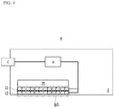
- FIG. 4 illustrates a BMS circuit according to a fourth embodiment.
- a BMS circuit 4 includes, on a substrate S, a controller a, a first resistor part 11 including a plurality of resistors r, a second resistor part 12 including a plurality of resistors r, a connector c that electrically connects the BMS circuit 1 to the outside, and a current path p connecting the controller a, the first resistor part 11, the second resistor part 12, and the connector.
- the controller a, the first resistor part 11, and the second resistor part 12 mounted on the BMS circuit 4 according to the fourth embodiment are the same as those mounted on the BMS circuit 1 according to the first embodiment, but their positions are different.
- the first resistor part 11 and the second resistor part 12 may be disposed in a direction (a horizontal direction in FIG. 4 ) parallel to the substrate S at a lower position of the substrate S of the BMS circuit 4, and a fifth perforation 25 may be formed on the substrate S at a position corresponding to an upper position of the first resistor part 11.
- the fifth perforation 25 may be generated by forming a hole in the substrate S in a longitudinal direction parallel to the first resistor part 11 and the second resistor part 12 so that heat generated from each of the plurality of resistors r may be diffused to be efficiently discharged.
- the BMS circuit 4 may include a third thermal pad tp3.
- the third thermal pad tp3 is attached to an upper surface each of the first resistor part 11 and the second resistor part 12 such that heat of the plurality of resistors r is efficiently conducted. Therefore, the heat of the plurality of resistors r may be diffused through the fifth perforation 25.
- the third thermal pad tp3 may have a shape wound at least once around the first resistor part 11, the second resistor part 12, and the lower surfaces of the substrate S while penetrating through the fifth perforation 25.
- the third thermal pad tp3 is wound around the first resistor part 11 and the second resistor part 12 so that it is attached to upper surfaces of the first resistor part 11 and the second resistor part 12, one side surface of the first resistor part 11, one side surface of the second resistor part 12, and lower surfaces of the first resistor part 11 and the second resistor part 12, but embodiments are not limited thereto.
Landscapes
- Engineering & Computer Science (AREA)
- Microelectronics & Electronic Packaging (AREA)
- Manufacturing & Machinery (AREA)
- Chemical & Material Sciences (AREA)
- Chemical Kinetics & Catalysis (AREA)
- Electrochemistry (AREA)
- General Chemical & Material Sciences (AREA)
- Physics & Mathematics (AREA)
- Thermal Sciences (AREA)
- Structure Of Printed Boards (AREA)
Applications Claiming Priority (2)
| Application Number | Priority Date | Filing Date | Title |
|---|---|---|---|
| KR1020190048580A KR102792206B1 (ko) | 2019-04-25 | 2019-04-25 | Bms 회로, bms 회로를 포함하는 배터리팩 |
| PCT/KR2020/003255 WO2020218735A1 (ko) | 2019-04-25 | 2020-03-09 | 배터리 관리 시스템 회로 |
Publications (2)
| Publication Number | Publication Date |
|---|---|
| EP3833162A1 true EP3833162A1 (de) | 2021-06-09 |
| EP3833162A4 EP3833162A4 (de) | 2021-12-08 |
Family
ID=72941622
Family Applications (1)
| Application Number | Title | Priority Date | Filing Date |
|---|---|---|---|
| EP20794150.1A Pending EP3833162A4 (de) | 2019-04-25 | 2020-03-09 | Schaltkreis eines batterieverwaltungssystems |
Country Status (6)
| Country | Link |
|---|---|
| US (1) | US11950353B2 (de) |
| EP (1) | EP3833162A4 (de) |
| JP (1) | JP7200469B2 (de) |
| KR (1) | KR102792206B1 (de) |
| CN (1) | CN214675832U (de) |
| WO (1) | WO2020218735A1 (de) |
Families Citing this family (1)
| Publication number | Priority date | Publication date | Assignee | Title |
|---|---|---|---|---|
| CN119967778B (zh) * | 2025-02-08 | 2026-01-02 | 奇瑞新能源汽车股份有限公司 | 一种电池管理系统、电池及汽车 |
Family Cites Families (22)
| Publication number | Priority date | Publication date | Assignee | Title |
|---|---|---|---|---|
| US4658234A (en) | 1984-06-06 | 1987-04-14 | Alps Electric Co., Ltd. | Resistor network |
| JPH03296292A (ja) | 1990-04-13 | 1991-12-26 | Taiyo Yuden Co Ltd | 混成集積回路部品 |
| JPH04255289A (ja) | 1991-02-07 | 1992-09-10 | Nec Corp | 金属ベース配線基板 |
| JP2925475B2 (ja) | 1995-10-06 | 1999-07-28 | 東光株式会社 | 電子装置の放熱構造 |
| KR200349181Y1 (ko) | 1998-12-31 | 2004-09-24 | 한라공조주식회사 | 저항기의방열장치 |
| JP2005223078A (ja) * | 2004-02-04 | 2005-08-18 | Murata Mfg Co Ltd | 回路モジュール |
| JP2006173243A (ja) * | 2004-12-14 | 2006-06-29 | Fujitsu Ten Ltd | プリント配線板、及びプリント回路板の放熱構造 |
| JP4448111B2 (ja) | 2006-07-31 | 2010-04-07 | 日立ビークルエナジー株式会社 | 電源システム |
| WO2009096966A1 (en) | 2008-01-31 | 2009-08-06 | Hewlett-Packard Development Company, L.P. | Insulating aperture in printed circuit boards |
| DE102008060487A1 (de) | 2008-12-05 | 2010-06-10 | Sennheiser Electronic Gmbh & Co. Kg | Elektronisches Gerät und Leiterplatte |
| JPWO2011024477A1 (ja) * | 2009-08-31 | 2013-01-24 | 三洋電機株式会社 | バッテリモジュール、バッテリシステムおよび電動車両 |
| JP2012204783A (ja) | 2011-03-28 | 2012-10-22 | Stanley Electric Co Ltd | 発光ダイオード装置 |
| KR101658025B1 (ko) * | 2011-11-02 | 2016-09-21 | 삼성에스디아이 주식회사 | 이차전지 |
| US20130170136A1 (en) * | 2011-12-31 | 2013-07-04 | Joshua L. Roby | Pcb heat sink for power electronics |
| JP2013230024A (ja) * | 2012-04-26 | 2013-11-07 | Toyota Motor Corp | 並列電池の制御装置 |
| US10270141B2 (en) | 2013-01-30 | 2019-04-23 | Gentherm Incorporated | Thermoelectric-based thermal management system |
| JP6184242B2 (ja) | 2013-08-09 | 2017-08-23 | 株式会社東芝 | 基板および組電池モジュール |
| KR101733088B1 (ko) | 2015-03-23 | 2017-05-08 | 주식회사 코캄 | 효율적인 온도 검출이 가능한 구조를 갖는 배터리 팩 및 이에 적용되는 온도 소자 실장형 인쇄회로기판 |
| JP2017050478A (ja) | 2015-09-04 | 2017-03-09 | Koa株式会社 | 抵抗器 |
| WO2017174336A1 (en) * | 2016-04-04 | 2017-10-12 | Philips Lighting Holding B.V. | Pcb assembly with fasteners |
| CN206365129U (zh) | 2016-12-15 | 2017-07-28 | 北京小鸟看看科技有限公司 | 用于发热元器件的印制电路板、印制装配板及电子设备 |
| US10772242B2 (en) * | 2018-04-17 | 2020-09-08 | Chongqing Jinkang New Energy Vehicle Co., Ltd. | Inverter module of an electric vehicle |
-
2019
- 2019-04-25 KR KR1020190048580A patent/KR102792206B1/ko active Active
-
2020
- 2020-03-09 JP JP2021515131A patent/JP7200469B2/ja active Active
- 2020-03-09 WO PCT/KR2020/003255 patent/WO2020218735A1/ko not_active Ceased
- 2020-03-09 US US17/273,455 patent/US11950353B2/en active Active
- 2020-03-09 EP EP20794150.1A patent/EP3833162A4/de active Pending
- 2020-03-09 CN CN202090000242.XU patent/CN214675832U/zh active Active
Also Published As
| Publication number | Publication date |
|---|---|
| CN214675832U (zh) | 2021-11-09 |
| US20210345480A1 (en) | 2021-11-04 |
| KR102792206B1 (ko) | 2025-04-04 |
| JP2022501816A (ja) | 2022-01-06 |
| US11950353B2 (en) | 2024-04-02 |
| JP7200469B2 (ja) | 2023-01-10 |
| EP3833162A4 (de) | 2021-12-08 |
| WO2020218735A1 (ko) | 2020-10-29 |
| KR20200124996A (ko) | 2020-11-04 |
Similar Documents
| Publication | Publication Date | Title |
|---|---|---|
| KR101953362B1 (ko) | 개선된 체결구조를 갖는 배터리 모듈 | |
| US11309604B2 (en) | Thermal epoxy and positioning of electrochemical cells | |
| CN105591048B (zh) | 用于袋式电池单元的牵引电池汇流条支架 | |
| US10059222B2 (en) | Battery temperature estimation system | |
| US8922959B2 (en) | Safety component by fuse at high voltage battery sensing line | |
| US20110151315A1 (en) | Bus bar assembly | |
| EP3201039B1 (de) | Integrierter verbinder mit mess- und schaltleitern für ein relais in einem batteriemodul | |
| CN102299267B (zh) | 集成有测量传感器线路和均衡电阻的蓄电池组电池 | |
| KR101636444B1 (ko) | 전지모듈 및 이를 포함하는 전지팩 | |
| JP2008186595A (ja) | 2次電池 | |
| KR20130025245A (ko) | 전지모듈 | |
| EP3046165B1 (de) | Batteriemodul mit erfassungsmodulen mit verbesserter kopplungsstruktur | |
| KR101527546B1 (ko) | 배터리 관리 시스템과 이를 포함하는 배터리 팩 보호 장치 | |
| KR102647282B1 (ko) | 배터리 모듈 | |
| WO2019071184A1 (en) | LITHIUM ION BATTERY | |
| CN115732778A (zh) | 用于电池管理的系统和方法 | |
| JP2008284946A (ja) | 電池ユニットの車両搭載構造 | |
| JP2010015903A (ja) | 二次電池装置 | |
| EP3833162A1 (de) | Schaltkreis eines batterieverwaltungssystems | |
| KR20180094632A (ko) | 배터리 모듈, 이러한 배터리 모듈을 포함하는 배터리 팩 및 이러한 배터리 팩을 포함하는 자동차 | |
| US9494652B2 (en) | Voltage and temperature sensing of battery cell groups | |
| CN108112274B (zh) | 电池组模块的传感器压紧指状物 | |
| KR20220006474A (ko) | 배터리 시스템 및 배터리 시스템을 충전하는 방법 | |
| JP6311591B2 (ja) | 電池ユニット | |
| US9553288B2 (en) | Step configuration for traction battery housing |
Legal Events
| Date | Code | Title | Description |
|---|---|---|---|
| STAA | Information on the status of an ep patent application or granted ep patent |
Free format text: STATUS: THE INTERNATIONAL PUBLICATION HAS BEEN MADE |
|
| PUAI | Public reference made under article 153(3) epc to a published international application that has entered the european phase |
Free format text: ORIGINAL CODE: 0009012 |
|
| STAA | Information on the status of an ep patent application or granted ep patent |
Free format text: STATUS: REQUEST FOR EXAMINATION WAS MADE |
|
| 17P | Request for examination filed |
Effective date: 20210305 |
|
| AK | Designated contracting states |
Kind code of ref document: A1 Designated state(s): AL AT BE BG CH CY CZ DE DK EE ES FI FR GB GR HR HU IE IS IT LI LT LU LV MC MK MT NL NO PL PT RO RS SE SI SK SM TR |
|
| A4 | Supplementary search report drawn up and despatched |
Effective date: 20211109 |
|
| RIC1 | Information provided on ipc code assigned before grant |
Ipc: H01M 10/42 20060101ALI20211103BHEP Ipc: H05K 7/20 20060101ALI20211103BHEP Ipc: H05K 1/02 20060101AFI20211103BHEP |
|
| RAP1 | Party data changed (applicant data changed or rights of an application transferred) |
Owner name: LG ENERGY SOLUTION LTD. |
|
| RAP3 | Party data changed (applicant data changed or rights of an application transferred) |
Owner name: LG ENERGY SOLUTION, LTD. |
|
| DAV | Request for validation of the european patent (deleted) | ||
| DAX | Request for extension of the european patent (deleted) | ||
| STAA | Information on the status of an ep patent application or granted ep patent |
Free format text: STATUS: EXAMINATION IS IN PROGRESS |
|
| 17Q | First examination report despatched |
Effective date: 20240910 |