EP3778890B1 - Strukturierte substrate zur verbesserten detektion von lichtemissionen und verfahren im zusammenhang damit - Google Patents
Strukturierte substrate zur verbesserten detektion von lichtemissionen und verfahren im zusammenhang damit Download PDFInfo
- Publication number
- EP3778890B1 EP3778890B1 EP20200233.3A EP20200233A EP3778890B1 EP 3778890 B1 EP3778890 B1 EP 3778890B1 EP 20200233 A EP20200233 A EP 20200233A EP 3778890 B1 EP3778890 B1 EP 3778890B1
- Authority
- EP
- European Patent Office
- Prior art keywords
- nanostructures
- layer
- reaction
- cavity
- ensemble
- Prior art date
- Legal status (The legal status is an assumption and is not a legal conclusion. Google has not performed a legal analysis and makes no representation as to the accuracy of the status listed.)
- Active
Links
- 238000000034 method Methods 0.000 title claims description 230
- 239000000758 substrate Substances 0.000 title claims description 155
- 230000023077 detection of light stimulus Effects 0.000 title 1
- 239000002086 nanomaterial Substances 0.000 claims description 326
- 238000006243 chemical reaction Methods 0.000 claims description 282
- 239000000463 material Substances 0.000 claims description 216
- 239000010931 gold Substances 0.000 claims description 81
- 239000011368 organic material Substances 0.000 claims description 60
- 238000004519 manufacturing process Methods 0.000 claims description 46
- 229910052710 silicon Inorganic materials 0.000 claims description 34
- 239000010703 silicon Substances 0.000 claims description 34
- KDLHZDBZIXYQEI-UHFFFAOYSA-N Palladium Chemical compound [Pd] KDLHZDBZIXYQEI-UHFFFAOYSA-N 0.000 claims description 33
- BASFCYQUMIYNBI-UHFFFAOYSA-N platinum Chemical compound [Pt] BASFCYQUMIYNBI-UHFFFAOYSA-N 0.000 claims description 33
- 239000000203 mixture Substances 0.000 claims description 26
- 229910052737 gold Inorganic materials 0.000 claims description 23
- 239000011651 chromium Substances 0.000 claims description 22
- 239000010949 copper Substances 0.000 claims description 22
- 239000010948 rhodium Substances 0.000 claims description 22
- 239000010936 titanium Substances 0.000 claims description 22
- PCHJSUWPFVWCPO-UHFFFAOYSA-N gold Chemical compound [Au] PCHJSUWPFVWCPO-UHFFFAOYSA-N 0.000 claims description 21
- 230000010287 polarization Effects 0.000 claims description 16
- 229910052709 silver Inorganic materials 0.000 claims description 15
- BQCADISMDOOEFD-UHFFFAOYSA-N Silver Chemical compound [Ag] BQCADISMDOOEFD-UHFFFAOYSA-N 0.000 claims description 13
- 239000004332 silver Substances 0.000 claims description 13
- JBRZTFJDHDCESZ-UHFFFAOYSA-N AsGa Chemical compound [As]#[Ga] JBRZTFJDHDCESZ-UHFFFAOYSA-N 0.000 claims description 12
- VYZAMTAEIAYCRO-UHFFFAOYSA-N Chromium Chemical compound [Cr] VYZAMTAEIAYCRO-UHFFFAOYSA-N 0.000 claims description 12
- 229910001218 Gallium arsenide Inorganic materials 0.000 claims description 12
- RYGMFSIKBFXOCR-UHFFFAOYSA-N Copper Chemical compound [Cu] RYGMFSIKBFXOCR-UHFFFAOYSA-N 0.000 claims description 11
- KJTLSVCANCCWHF-UHFFFAOYSA-N Ruthenium Chemical compound [Ru] KJTLSVCANCCWHF-UHFFFAOYSA-N 0.000 claims description 11
- ATJFFYVFTNAWJD-UHFFFAOYSA-N Tin Chemical compound [Sn] ATJFFYVFTNAWJD-UHFFFAOYSA-N 0.000 claims description 11
- RTAQQCXQSZGOHL-UHFFFAOYSA-N Titanium Chemical compound [Ti] RTAQQCXQSZGOHL-UHFFFAOYSA-N 0.000 claims description 11
- 229910052782 aluminium Inorganic materials 0.000 claims description 11
- XAGFODPZIPBFFR-UHFFFAOYSA-N aluminium Chemical compound [Al] XAGFODPZIPBFFR-UHFFFAOYSA-N 0.000 claims description 11
- 229910052804 chromium Inorganic materials 0.000 claims description 11
- 229910052802 copper Inorganic materials 0.000 claims description 11
- 229910052741 iridium Inorganic materials 0.000 claims description 11
- GKOZUEZYRPOHIO-UHFFFAOYSA-N iridium atom Chemical compound [Ir] GKOZUEZYRPOHIO-UHFFFAOYSA-N 0.000 claims description 11
- 229910052762 osmium Inorganic materials 0.000 claims description 11
- SYQBFIAQOQZEGI-UHFFFAOYSA-N osmium atom Chemical compound [Os] SYQBFIAQOQZEGI-UHFFFAOYSA-N 0.000 claims description 11
- 229910052763 palladium Inorganic materials 0.000 claims description 11
- 229910052697 platinum Inorganic materials 0.000 claims description 11
- 229910052703 rhodium Inorganic materials 0.000 claims description 11
- MHOVAHRLVXNVSD-UHFFFAOYSA-N rhodium atom Chemical compound [Rh] MHOVAHRLVXNVSD-UHFFFAOYSA-N 0.000 claims description 11
- 229910052707 ruthenium Inorganic materials 0.000 claims description 11
- 229910052719 titanium Inorganic materials 0.000 claims description 11
- 239000000017 hydrogel Substances 0.000 claims description 9
- 230000001902 propagating effect Effects 0.000 claims description 9
- 230000007717 exclusion Effects 0.000 claims description 8
- 230000004044 response Effects 0.000 claims description 7
- 238000010899 nucleation Methods 0.000 claims description 5
- 239000010410 layer Substances 0.000 description 204
- 239000002105 nanoparticle Substances 0.000 description 140
- 238000001127 nanoimprint lithography Methods 0.000 description 94
- 239000000499 gel Substances 0.000 description 93
- 102000039446 nucleic acids Human genes 0.000 description 92
- 108020004707 nucleic acids Proteins 0.000 description 92
- 150000007523 nucleic acids Chemical class 0.000 description 92
- 239000007787 solid Substances 0.000 description 77
- 238000012163 sequencing technique Methods 0.000 description 45
- 230000008569 process Effects 0.000 description 35
- 239000000523 sample Substances 0.000 description 34
- XUIMIQQOPSSXEZ-UHFFFAOYSA-N Silicon Chemical compound [Si] XUIMIQQOPSSXEZ-UHFFFAOYSA-N 0.000 description 32
- 125000003729 nucleotide group Chemical group 0.000 description 32
- 239000002773 nucleotide Substances 0.000 description 31
- 239000000126 substance Substances 0.000 description 29
- 238000000151 deposition Methods 0.000 description 28
- 230000005284 excitation Effects 0.000 description 27
- 229910052751 metal Inorganic materials 0.000 description 27
- 239000002184 metal Substances 0.000 description 27
- 210000004027 cell Anatomy 0.000 description 23
- 230000008021 deposition Effects 0.000 description 22
- 239000010408 film Substances 0.000 description 22
- 239000007788 liquid Substances 0.000 description 22
- 238000005498 polishing Methods 0.000 description 22
- 238000001514 detection method Methods 0.000 description 21
- 108010003723 Single-Domain Antibodies Proteins 0.000 description 19
- VYPSYNLAJGMNEJ-UHFFFAOYSA-N Silicium dioxide Chemical compound O=[Si]=O VYPSYNLAJGMNEJ-UHFFFAOYSA-N 0.000 description 18
- 108020004414 DNA Proteins 0.000 description 16
- 102000053602 DNA Human genes 0.000 description 16
- 230000015572 biosynthetic process Effects 0.000 description 15
- 238000003786 synthesis reaction Methods 0.000 description 15
- 239000002063 nanoring Substances 0.000 description 14
- 239000002245 particle Substances 0.000 description 14
- 229920000642 polymer Polymers 0.000 description 13
- 230000003321 amplification Effects 0.000 description 11
- 239000000539 dimer Substances 0.000 description 11
- 238000005530 etching Methods 0.000 description 11
- 239000011521 glass Substances 0.000 description 11
- 238000009396 hybridization Methods 0.000 description 11
- 238000003199 nucleic acid amplification method Methods 0.000 description 11
- 238000002161 passivation Methods 0.000 description 11
- 238000003491 array Methods 0.000 description 10
- 238000000137 annealing Methods 0.000 description 9
- 230000008901 benefit Effects 0.000 description 9
- 239000011248 coating agent Substances 0.000 description 9
- 238000000576 coating method Methods 0.000 description 9
- 239000007789 gas Substances 0.000 description 9
- 230000003287 optical effect Effects 0.000 description 9
- 238000002198 surface plasmon resonance spectroscopy Methods 0.000 description 9
- 239000013638 trimer Substances 0.000 description 9
- 108091034117 Oligonucleotide Proteins 0.000 description 8
- 108020005187 Oligonucleotide Probes Proteins 0.000 description 8
- BLRPTPMANUNPDV-UHFFFAOYSA-N Silane Chemical compound [SiH4] BLRPTPMANUNPDV-UHFFFAOYSA-N 0.000 description 8
- 239000000654 additive Substances 0.000 description 8
- 230000000996 additive effect Effects 0.000 description 8
- 239000003153 chemical reaction reagent Substances 0.000 description 8
- 238000005516 engineering process Methods 0.000 description 8
- 238000003384 imaging method Methods 0.000 description 8
- -1 nanopyramids Substances 0.000 description 8
- 239000002751 oligonucleotide probe Substances 0.000 description 8
- 229910000077 silane Inorganic materials 0.000 description 8
- 239000000377 silicon dioxide Substances 0.000 description 8
- 230000000694 effects Effects 0.000 description 7
- 238000001878 scanning electron micrograph Methods 0.000 description 7
- 238000004458 analytical method Methods 0.000 description 6
- 239000011324 bead Substances 0.000 description 6
- 230000006872 improvement Effects 0.000 description 6
- 238000010348 incorporation Methods 0.000 description 6
- 238000003754 machining Methods 0.000 description 6
- 239000002073 nanorod Substances 0.000 description 6
- 239000002077 nanosphere Substances 0.000 description 6
- 239000002070 nanowire Substances 0.000 description 6
- 238000012175 pyrosequencing Methods 0.000 description 6
- 230000005855 radiation Effects 0.000 description 6
- 241000894007 species Species 0.000 description 6
- 238000004528 spin coating Methods 0.000 description 6
- 238000005229 chemical vapour deposition Methods 0.000 description 5
- 239000000975 dye Substances 0.000 description 5
- 238000001338 self-assembly Methods 0.000 description 5
- 238000004544 sputter deposition Methods 0.000 description 5
- 102000004190 Enzymes Human genes 0.000 description 4
- 108090000790 Enzymes Proteins 0.000 description 4
- 150000001875 compounds Chemical class 0.000 description 4
- OPTASPLRGRRNAP-UHFFFAOYSA-N cytosine Chemical compound NC=1C=CNC(=O)N=1 OPTASPLRGRRNAP-UHFFFAOYSA-N 0.000 description 4
- 230000007423 decrease Effects 0.000 description 4
- 238000004070 electrodeposition Methods 0.000 description 4
- 238000001704 evaporation Methods 0.000 description 4
- 230000008020 evaporation Effects 0.000 description 4
- 230000001747 exhibiting effect Effects 0.000 description 4
- 238000002474 experimental method Methods 0.000 description 4
- 238000001506 fluorescence spectroscopy Methods 0.000 description 4
- 230000014509 gene expression Effects 0.000 description 4
- UYTPUPDQBNUYGX-UHFFFAOYSA-N guanine Chemical compound O=C1NC(N)=NC2=C1N=CN2 UYTPUPDQBNUYGX-UHFFFAOYSA-N 0.000 description 4
- 230000003993 interaction Effects 0.000 description 4
- 230000000670 limiting effect Effects 0.000 description 4
- 150000002739 metals Chemical class 0.000 description 4
- 239000002078 nanoshell Substances 0.000 description 4
- 238000005240 physical vapour deposition Methods 0.000 description 4
- 239000004033 plastic Substances 0.000 description 4
- 229920003023 plastic Polymers 0.000 description 4
- 238000012545 processing Methods 0.000 description 4
- 238000011160 research Methods 0.000 description 4
- 239000011800 void material Substances 0.000 description 4
- ZKHQWZAMYRWXGA-KQYNXXCUSA-J ATP(4-) Chemical compound C1=NC=2C(N)=NC=NC=2N1[C@@H]1O[C@H](COP([O-])(=O)OP([O-])(=O)OP([O-])([O-])=O)[C@@H](O)[C@H]1O ZKHQWZAMYRWXGA-KQYNXXCUSA-J 0.000 description 3
- ZKHQWZAMYRWXGA-UHFFFAOYSA-N Adenosine triphosphate Natural products C1=NC=2C(N)=NC=NC=2N1C1OC(COP(O)(=O)OP(O)(=O)OP(O)(O)=O)C(O)C1O ZKHQWZAMYRWXGA-UHFFFAOYSA-N 0.000 description 3
- 238000003559 RNA-seq method Methods 0.000 description 3
- 239000012491 analyte Substances 0.000 description 3
- 238000013459 approach Methods 0.000 description 3
- 238000000231 atomic layer deposition Methods 0.000 description 3
- 238000005266 casting Methods 0.000 description 3
- 230000001419 dependent effect Effects 0.000 description 3
- XPPKVPWEQAFLFU-UHFFFAOYSA-J diphosphate(4-) Chemical compound [O-]P([O-])(=O)OP([O-])([O-])=O XPPKVPWEQAFLFU-UHFFFAOYSA-J 0.000 description 3
- 235000011180 diphosphates Nutrition 0.000 description 3
- 238000009826 distribution Methods 0.000 description 3
- 238000001035 drying Methods 0.000 description 3
- 230000002708 enhancing effect Effects 0.000 description 3
- 238000000407 epitaxy Methods 0.000 description 3
- 239000012530 fluid Substances 0.000 description 3
- 238000002866 fluorescence resonance energy transfer Methods 0.000 description 3
- 238000000227 grinding Methods 0.000 description 3
- 150000002500 ions Chemical class 0.000 description 3
- 238000004518 low pressure chemical vapour deposition Methods 0.000 description 3
- 239000007769 metal material Substances 0.000 description 3
- 238000012986 modification Methods 0.000 description 3
- 230000004048 modification Effects 0.000 description 3
- 238000003499 nucleic acid array Methods 0.000 description 3
- 239000013307 optical fiber Substances 0.000 description 3
- 230000003647 oxidation Effects 0.000 description 3
- 238000007254 oxidation reaction Methods 0.000 description 3
- 238000000206 photolithography Methods 0.000 description 3
- 238000000623 plasma-assisted chemical vapour deposition Methods 0.000 description 3
- 230000002829 reductive effect Effects 0.000 description 3
- 230000002441 reversible effect Effects 0.000 description 3
- 229920002477 rna polymer Polymers 0.000 description 3
- 238000000926 separation method Methods 0.000 description 3
- 238000007841 sequencing by ligation Methods 0.000 description 3
- 239000002002 slurry Substances 0.000 description 3
- 229930024421 Adenine Natural products 0.000 description 2
- GFFGJBXGBJISGV-UHFFFAOYSA-N Adenine Chemical compound NC1=NC=NC2=C1N=CN2 GFFGJBXGBJISGV-UHFFFAOYSA-N 0.000 description 2
- 229920000936 Agarose Polymers 0.000 description 2
- XKRFYHLGVUSROY-UHFFFAOYSA-N Argon Chemical compound [Ar] XKRFYHLGVUSROY-UHFFFAOYSA-N 0.000 description 2
- IJGRMHOSHXDMSA-UHFFFAOYSA-N Atomic nitrogen Chemical compound N#N IJGRMHOSHXDMSA-UHFFFAOYSA-N 0.000 description 2
- OKTJSMMVPCPJKN-UHFFFAOYSA-N Carbon Chemical compound [C] OKTJSMMVPCPJKN-UHFFFAOYSA-N 0.000 description 2
- 102000016928 DNA-directed DNA polymerase Human genes 0.000 description 2
- 108010014303 DNA-directed DNA polymerase Proteins 0.000 description 2
- 108010010803 Gelatin Proteins 0.000 description 2
- PPBRXRYQALVLMV-UHFFFAOYSA-N Styrene Chemical compound C=CC1=CC=CC=C1 PPBRXRYQALVLMV-UHFFFAOYSA-N 0.000 description 2
- ISAKRJDGNUQOIC-UHFFFAOYSA-N Uracil Chemical compound O=C1C=CNC(=O)N1 ISAKRJDGNUQOIC-UHFFFAOYSA-N 0.000 description 2
- 229960000643 adenine Drugs 0.000 description 2
- 230000002411 adverse Effects 0.000 description 2
- 238000001505 atmospheric-pressure chemical vapour deposition Methods 0.000 description 2
- 229920001222 biopolymer Polymers 0.000 description 2
- 229910052799 carbon Inorganic materials 0.000 description 2
- 238000003486 chemical etching Methods 0.000 description 2
- 229910052681 coesite Inorganic materials 0.000 description 2
- 238000005859 coupling reaction Methods 0.000 description 2
- 229910052906 cristobalite Inorganic materials 0.000 description 2
- 229920006037 cross link polymer Polymers 0.000 description 2
- 125000004122 cyclic group Chemical group 0.000 description 2
- 229940104302 cytosine Drugs 0.000 description 2
- 238000005137 deposition process Methods 0.000 description 2
- 201000010099 disease Diseases 0.000 description 2
- 208000037265 diseases, disorders, signs and symptoms Diseases 0.000 description 2
- 238000005566 electron beam evaporation Methods 0.000 description 2
- ZZUFCTLCJUWOSV-UHFFFAOYSA-N furosemide Chemical compound C1=C(Cl)C(S(=O)(=O)N)=CC(C(O)=O)=C1NCC1=CC=CO1 ZZUFCTLCJUWOSV-UHFFFAOYSA-N 0.000 description 2
- 239000008273 gelatin Substances 0.000 description 2
- 229920000159 gelatin Polymers 0.000 description 2
- 235000019322 gelatine Nutrition 0.000 description 2
- 235000011852 gelatine desserts Nutrition 0.000 description 2
- 230000005484 gravity Effects 0.000 description 2
- 230000000415 inactivating effect Effects 0.000 description 2
- 238000007373 indentation Methods 0.000 description 2
- 238000001182 laser chemical vapour deposition Methods 0.000 description 2
- 238000011068 loading method Methods 0.000 description 2
- 239000013528 metallic particle Substances 0.000 description 2
- 238000007837 multiplex assay Methods 0.000 description 2
- 238000005329 nanolithography Methods 0.000 description 2
- 239000002071 nanotube Substances 0.000 description 2
- 229910052755 nonmetal Inorganic materials 0.000 description 2
- 229920000620 organic polymer Polymers 0.000 description 2
- 229920002401 polyacrylamide Polymers 0.000 description 2
- 238000006116 polymerization reaction Methods 0.000 description 2
- 108090000623 proteins and genes Proteins 0.000 description 2
- 102000004169 proteins and genes Human genes 0.000 description 2
- 230000009467 reduction Effects 0.000 description 2
- 239000013545 self-assembled monolayer Substances 0.000 description 2
- 238000004557 single molecule detection Methods 0.000 description 2
- 239000007790 solid phase Substances 0.000 description 2
- 239000012798 spherical particle Substances 0.000 description 2
- 238000009718 spray deposition Methods 0.000 description 2
- 238000000992 sputter etching Methods 0.000 description 2
- 239000007858 starting material Substances 0.000 description 2
- 238000001494 step-and-flash imprint lithography Methods 0.000 description 2
- 229910052682 stishovite Inorganic materials 0.000 description 2
- RWQNBRDOKXIBIV-UHFFFAOYSA-N thymine Chemical compound CC1=CNC(=O)NC1=O RWQNBRDOKXIBIV-UHFFFAOYSA-N 0.000 description 2
- 238000012546 transfer Methods 0.000 description 2
- 229910052905 tridymite Inorganic materials 0.000 description 2
- 238000000038 ultrahigh vacuum chemical vapour deposition Methods 0.000 description 2
- ASJSAQIRZKANQN-CRCLSJGQSA-N 2-deoxy-D-ribose Chemical compound OC[C@@H](O)[C@@H](O)CC=O ASJSAQIRZKANQN-CRCLSJGQSA-N 0.000 description 1
- PHIYHIOQVWTXII-UHFFFAOYSA-N 3-amino-1-phenylpropan-1-ol Chemical compound NCCC(O)C1=CC=CC=C1 PHIYHIOQVWTXII-UHFFFAOYSA-N 0.000 description 1
- HRPVXLWXLXDGHG-UHFFFAOYSA-N Acrylamide Chemical compound NC(=O)C=C HRPVXLWXLXDGHG-UHFFFAOYSA-N 0.000 description 1
- 108091093088 Amplicon Proteins 0.000 description 1
- 229920000089 Cyclic olefin copolymer Polymers 0.000 description 1
- HMFHBZSHGGEWLO-SOOFDHNKSA-N D-ribofuranose Chemical compound OC[C@H]1OC(O)[C@H](O)[C@@H]1O HMFHBZSHGGEWLO-SOOFDHNKSA-N 0.000 description 1
- 238000001712 DNA sequencing Methods 0.000 description 1
- 208000030453 Drug-Related Side Effects and Adverse reaction Diseases 0.000 description 1
- 239000004593 Epoxy Substances 0.000 description 1
- 102000003960 Ligases Human genes 0.000 description 1
- 108090000364 Ligases Proteins 0.000 description 1
- 239000004677 Nylon Substances 0.000 description 1
- 229910019142 PO4 Inorganic materials 0.000 description 1
- 239000004698 Polyethylene Substances 0.000 description 1
- 239000004642 Polyimide Substances 0.000 description 1
- 229920000388 Polyphosphate Polymers 0.000 description 1
- 239000004743 Polypropylene Substances 0.000 description 1
- 239000004793 Polystyrene Substances 0.000 description 1
- PYMYPHUHKUWMLA-LMVFSUKVSA-N Ribose Natural products OC[C@@H](O)[C@@H](O)[C@@H](O)C=O PYMYPHUHKUWMLA-LMVFSUKVSA-N 0.000 description 1
- 102000004523 Sulfate Adenylyltransferase Human genes 0.000 description 1
- 108010022348 Sulfate adenylyltransferase Proteins 0.000 description 1
- 239000004809 Teflon Substances 0.000 description 1
- 238000001015 X-ray lithography Methods 0.000 description 1
- JLCPHMBAVCMARE-UHFFFAOYSA-N [3-[[3-[[3-[[3-[[3-[[3-[[3-[[3-[[3-[[3-[[3-[[5-(2-amino-6-oxo-1H-purin-9-yl)-3-[[3-[[3-[[3-[[3-[[3-[[5-(2-amino-6-oxo-1H-purin-9-yl)-3-[[5-(2-amino-6-oxo-1H-purin-9-yl)-3-hydroxyoxolan-2-yl]methoxy-hydroxyphosphoryl]oxyoxolan-2-yl]methoxy-hydroxyphosphoryl]oxy-5-(5-methyl-2,4-dioxopyrimidin-1-yl)oxolan-2-yl]methoxy-hydroxyphosphoryl]oxy-5-(6-aminopurin-9-yl)oxolan-2-yl]methoxy-hydroxyphosphoryl]oxy-5-(6-aminopurin-9-yl)oxolan-2-yl]methoxy-hydroxyphosphoryl]oxy-5-(6-aminopurin-9-yl)oxolan-2-yl]methoxy-hydroxyphosphoryl]oxy-5-(6-aminopurin-9-yl)oxolan-2-yl]methoxy-hydroxyphosphoryl]oxyoxolan-2-yl]methoxy-hydroxyphosphoryl]oxy-5-(5-methyl-2,4-dioxopyrimidin-1-yl)oxolan-2-yl]methoxy-hydroxyphosphoryl]oxy-5-(4-amino-2-oxopyrimidin-1-yl)oxolan-2-yl]methoxy-hydroxyphosphoryl]oxy-5-(5-methyl-2,4-dioxopyrimidin-1-yl)oxolan-2-yl]methoxy-hydroxyphosphoryl]oxy-5-(5-methyl-2,4-dioxopyrimidin-1-yl)oxolan-2-yl]methoxy-hydroxyphosphoryl]oxy-5-(6-aminopurin-9-yl)oxolan-2-yl]methoxy-hydroxyphosphoryl]oxy-5-(6-aminopurin-9-yl)oxolan-2-yl]methoxy-hydroxyphosphoryl]oxy-5-(4-amino-2-oxopyrimidin-1-yl)oxolan-2-yl]methoxy-hydroxyphosphoryl]oxy-5-(4-amino-2-oxopyrimidin-1-yl)oxolan-2-yl]methoxy-hydroxyphosphoryl]oxy-5-(4-amino-2-oxopyrimidin-1-yl)oxolan-2-yl]methoxy-hydroxyphosphoryl]oxy-5-(6-aminopurin-9-yl)oxolan-2-yl]methoxy-hydroxyphosphoryl]oxy-5-(4-amino-2-oxopyrimidin-1-yl)oxolan-2-yl]methyl [5-(6-aminopurin-9-yl)-2-(hydroxymethyl)oxolan-3-yl] hydrogen phosphate Polymers Cc1cn(C2CC(OP(O)(=O)OCC3OC(CC3OP(O)(=O)OCC3OC(CC3O)n3cnc4c3nc(N)[nH]c4=O)n3cnc4c3nc(N)[nH]c4=O)C(COP(O)(=O)OC3CC(OC3COP(O)(=O)OC3CC(OC3COP(O)(=O)OC3CC(OC3COP(O)(=O)OC3CC(OC3COP(O)(=O)OC3CC(OC3COP(O)(=O)OC3CC(OC3COP(O)(=O)OC3CC(OC3COP(O)(=O)OC3CC(OC3COP(O)(=O)OC3CC(OC3COP(O)(=O)OC3CC(OC3COP(O)(=O)OC3CC(OC3COP(O)(=O)OC3CC(OC3COP(O)(=O)OC3CC(OC3COP(O)(=O)OC3CC(OC3COP(O)(=O)OC3CC(OC3COP(O)(=O)OC3CC(OC3COP(O)(=O)OC3CC(OC3CO)n3cnc4c(N)ncnc34)n3ccc(N)nc3=O)n3cnc4c(N)ncnc34)n3ccc(N)nc3=O)n3ccc(N)nc3=O)n3ccc(N)nc3=O)n3cnc4c(N)ncnc34)n3cnc4c(N)ncnc34)n3cc(C)c(=O)[nH]c3=O)n3cc(C)c(=O)[nH]c3=O)n3ccc(N)nc3=O)n3cc(C)c(=O)[nH]c3=O)n3cnc4c3nc(N)[nH]c4=O)n3cnc4c(N)ncnc34)n3cnc4c(N)ncnc34)n3cnc4c(N)ncnc34)n3cnc4c(N)ncnc34)O2)c(=O)[nH]c1=O JLCPHMBAVCMARE-UHFFFAOYSA-N 0.000 description 1
- 238000005299 abrasion Methods 0.000 description 1
- 229920006397 acrylic thermoplastic Polymers 0.000 description 1
- 229910045601 alloy Inorganic materials 0.000 description 1
- 239000000956 alloy Substances 0.000 description 1
- HMFHBZSHGGEWLO-UHFFFAOYSA-N alpha-D-Furanose-Ribose Natural products OCC1OC(O)C(O)C1O HMFHBZSHGGEWLO-UHFFFAOYSA-N 0.000 description 1
- 238000002048 anodisation reaction Methods 0.000 description 1
- 239000000427 antigen Substances 0.000 description 1
- 102000036639 antigens Human genes 0.000 description 1
- 108091007433 antigens Proteins 0.000 description 1
- 229910052786 argon Inorganic materials 0.000 description 1
- 239000012620 biological material Substances 0.000 description 1
- 238000005415 bioluminescence Methods 0.000 description 1
- 230000029918 bioluminescence Effects 0.000 description 1
- 239000005352 borofloat Substances 0.000 description 1
- 150000001720 carbohydrates Chemical class 0.000 description 1
- 235000014633 carbohydrates Nutrition 0.000 description 1
- 239000000919 ceramic Substances 0.000 description 1
- 238000001311 chemical methods and process Methods 0.000 description 1
- 239000003795 chemical substances by application Substances 0.000 description 1
- 230000000295 complement effect Effects 0.000 description 1
- 238000000748 compression moulding Methods 0.000 description 1
- 229920001577 copolymer Polymers 0.000 description 1
- 230000008878 coupling Effects 0.000 description 1
- 238000010168 coupling process Methods 0.000 description 1
- 230000003247 decreasing effect Effects 0.000 description 1
- 238000009792 diffusion process Methods 0.000 description 1
- 238000011143 downstream manufacturing Methods 0.000 description 1
- 238000005553 drilling Methods 0.000 description 1
- 238000001312 dry etching Methods 0.000 description 1
- 230000005684 electric field Effects 0.000 description 1
- 238000009760 electrical discharge machining Methods 0.000 description 1
- 238000005401 electroluminescence Methods 0.000 description 1
- 238000010894 electron beam technology Methods 0.000 description 1
- 238000000313 electron-beam-induced deposition Methods 0.000 description 1
- 238000009713 electroplating Methods 0.000 description 1
- 125000003700 epoxy group Chemical group 0.000 description 1
- 238000010195 expression analysis Methods 0.000 description 1
- 239000004744 fabric Substances 0.000 description 1
- 239000007850 fluorescent dye Substances 0.000 description 1
- 239000012634 fragment Substances 0.000 description 1
- 239000005350 fused silica glass Substances 0.000 description 1
- 230000007614 genetic variation Effects 0.000 description 1
- 238000012268 genome sequencing Methods 0.000 description 1
- 238000003205 genotyping method Methods 0.000 description 1
- 150000004676 glycans Chemical class 0.000 description 1
- 238000002513 implantation Methods 0.000 description 1
- 230000001976 improved effect Effects 0.000 description 1
- 238000011065 in-situ storage Methods 0.000 description 1
- 230000001939 inductive effect Effects 0.000 description 1
- 239000011261 inert gas Substances 0.000 description 1
- 230000000977 initiatory effect Effects 0.000 description 1
- 238000007641 inkjet printing Methods 0.000 description 1
- 238000007733 ion plating Methods 0.000 description 1
- 238000010884 ion-beam technique Methods 0.000 description 1
- 230000001788 irregular Effects 0.000 description 1
- 238000011901 isothermal amplification Methods 0.000 description 1
- 238000003475 lamination Methods 0.000 description 1
- 238000000608 laser ablation Methods 0.000 description 1
- 239000003446 ligand Substances 0.000 description 1
- 238000004943 liquid phase epitaxy Methods 0.000 description 1
- 238000001459 lithography Methods 0.000 description 1
- 238000000504 luminescence detection Methods 0.000 description 1
- 239000000155 melt Substances 0.000 description 1
- 239000002082 metal nanoparticle Substances 0.000 description 1
- 238000002493 microarray Methods 0.000 description 1
- 238000000813 microcontact printing Methods 0.000 description 1
- 238000001053 micromoulding Methods 0.000 description 1
- 238000013508 migration Methods 0.000 description 1
- 230000005012 migration Effects 0.000 description 1
- 238000003801 milling Methods 0.000 description 1
- 238000001451 molecular beam epitaxy Methods 0.000 description 1
- 238000012544 monitoring process Methods 0.000 description 1
- 238000000465 moulding Methods 0.000 description 1
- 229910052757 nitrogen Inorganic materials 0.000 description 1
- 239000002777 nucleoside Substances 0.000 description 1
- 150000003833 nucleoside derivatives Chemical class 0.000 description 1
- 229920001778 nylon Polymers 0.000 description 1
- BPUBBGLMJRNUCC-UHFFFAOYSA-N oxygen(2-);tantalum(5+) Chemical compound [O-2].[O-2].[O-2].[O-2].[O-2].[Ta+5].[Ta+5] BPUBBGLMJRNUCC-UHFFFAOYSA-N 0.000 description 1
- 230000036961 partial effect Effects 0.000 description 1
- 238000000059 patterning Methods 0.000 description 1
- 239000008194 pharmaceutical composition Substances 0.000 description 1
- 239000010452 phosphate Substances 0.000 description 1
- 238000001259 photo etching Methods 0.000 description 1
- 229920003229 poly(methyl methacrylate) Polymers 0.000 description 1
- 229920001748 polybutylene Polymers 0.000 description 1
- 229920000647 polyepoxide Polymers 0.000 description 1
- 229920000573 polyethylene Polymers 0.000 description 1
- 229920001721 polyimide Polymers 0.000 description 1
- 102000040430 polynucleotide Human genes 0.000 description 1
- 108091033319 polynucleotide Proteins 0.000 description 1
- 239000002157 polynucleotide Substances 0.000 description 1
- 229920001184 polypeptide Polymers 0.000 description 1
- 239000001205 polyphosphate Substances 0.000 description 1
- 235000011176 polyphosphates Nutrition 0.000 description 1
- 229920001155 polypropylene Polymers 0.000 description 1
- 229920001282 polysaccharide Polymers 0.000 description 1
- 239000005017 polysaccharide Substances 0.000 description 1
- 229920002223 polystyrene Polymers 0.000 description 1
- 229920002635 polyurethane Polymers 0.000 description 1
- 239000004814 polyurethane Substances 0.000 description 1
- 239000000955 prescription drug Substances 0.000 description 1
- 108090000765 processed proteins & peptides Proteins 0.000 description 1
- 102000004196 processed proteins & peptides Human genes 0.000 description 1
- 238000004549 pulsed laser deposition Methods 0.000 description 1
- 239000010453 quartz Substances 0.000 description 1
- 238000005395 radioluminescence Methods 0.000 description 1
- 238000010107 reaction injection moulding Methods 0.000 description 1
- 230000009257 reactivity Effects 0.000 description 1
- 238000009877 rendering Methods 0.000 description 1
- 230000003252 repetitive effect Effects 0.000 description 1
- 230000010076 replication Effects 0.000 description 1
- 239000011347 resin Substances 0.000 description 1
- 229920005989 resin Polymers 0.000 description 1
- 230000004043 responsiveness Effects 0.000 description 1
- 239000010980 sapphire Substances 0.000 description 1
- 229910052594 sapphire Inorganic materials 0.000 description 1
- 238000007790 scraping Methods 0.000 description 1
- 238000012216 screening Methods 0.000 description 1
- 238000007493 shaping process Methods 0.000 description 1
- 150000003376 silicon Chemical class 0.000 description 1
- 239000011856 silicon-based particle Substances 0.000 description 1
- 239000002356 single layer Substances 0.000 description 1
- 150000003384 small molecules Chemical class 0.000 description 1
- 238000000348 solid-phase epitaxy Methods 0.000 description 1
- 239000000243 solution Substances 0.000 description 1
- 238000005118 spray pyrolysis Methods 0.000 description 1
- 238000005507 spraying Methods 0.000 description 1
- 229910001936 tantalum oxide Inorganic materials 0.000 description 1
- ISXSCDLOGDJUNJ-UHFFFAOYSA-N tert-butyl prop-2-enoate Chemical compound CC(C)(C)OC(=O)C=C ISXSCDLOGDJUNJ-UHFFFAOYSA-N 0.000 description 1
- 238000012360 testing method Methods 0.000 description 1
- 238000002560 therapeutic procedure Methods 0.000 description 1
- 238000002207 thermal evaporation Methods 0.000 description 1
- 239000010409 thin film Substances 0.000 description 1
- 229940113082 thymine Drugs 0.000 description 1
- 229940035893 uracil Drugs 0.000 description 1
- 238000007740 vapor deposition Methods 0.000 description 1
- 239000012808 vapor phase Substances 0.000 description 1
- 239000011345 viscous material Substances 0.000 description 1
- XLYOFNOQVPJJNP-UHFFFAOYSA-N water Substances O XLYOFNOQVPJJNP-UHFFFAOYSA-N 0.000 description 1
- 238000003631 wet chemical etching Methods 0.000 description 1
Images


Classifications
-
- C—CHEMISTRY; METALLURGY
- C12—BIOCHEMISTRY; BEER; SPIRITS; WINE; VINEGAR; MICROBIOLOGY; ENZYMOLOGY; MUTATION OR GENETIC ENGINEERING
- C12Q—MEASURING OR TESTING PROCESSES INVOLVING ENZYMES, NUCLEIC ACIDS OR MICROORGANISMS; COMPOSITIONS OR TEST PAPERS THEREFOR; PROCESSES OF PREPARING SUCH COMPOSITIONS; CONDITION-RESPONSIVE CONTROL IN MICROBIOLOGICAL OR ENZYMOLOGICAL PROCESSES
- C12Q1/00—Measuring or testing processes involving enzymes, nucleic acids or microorganisms; Compositions therefor; Processes of preparing such compositions
- C12Q1/68—Measuring or testing processes involving enzymes, nucleic acids or microorganisms; Compositions therefor; Processes of preparing such compositions involving nucleic acids
- C12Q1/6813—Hybridisation assays
- C12Q1/6834—Enzymatic or biochemical coupling of nucleic acids to a solid phase
-
- C—CHEMISTRY; METALLURGY
- C12—BIOCHEMISTRY; BEER; SPIRITS; WINE; VINEGAR; MICROBIOLOGY; ENZYMOLOGY; MUTATION OR GENETIC ENGINEERING
- C12Q—MEASURING OR TESTING PROCESSES INVOLVING ENZYMES, NUCLEIC ACIDS OR MICROORGANISMS; COMPOSITIONS OR TEST PAPERS THEREFOR; PROCESSES OF PREPARING SUCH COMPOSITIONS; CONDITION-RESPONSIVE CONTROL IN MICROBIOLOGICAL OR ENZYMOLOGICAL PROCESSES
- C12Q1/00—Measuring or testing processes involving enzymes, nucleic acids or microorganisms; Compositions therefor; Processes of preparing such compositions
- C12Q1/68—Measuring or testing processes involving enzymes, nucleic acids or microorganisms; Compositions therefor; Processes of preparing such compositions involving nucleic acids
- C12Q1/6844—Nucleic acid amplification reactions
-
- B—PERFORMING OPERATIONS; TRANSPORTING
- B01—PHYSICAL OR CHEMICAL PROCESSES OR APPARATUS IN GENERAL
- B01J—CHEMICAL OR PHYSICAL PROCESSES, e.g. CATALYSIS OR COLLOID CHEMISTRY; THEIR RELEVANT APPARATUS
- B01J19/00—Chemical, physical or physico-chemical processes in general; Their relevant apparatus
- B01J19/0046—Sequential or parallel reactions, e.g. for the synthesis of polypeptides or polynucleotides; Apparatus and devices for combinatorial chemistry or for making molecular arrays
-
- B—PERFORMING OPERATIONS; TRANSPORTING
- B01—PHYSICAL OR CHEMICAL PROCESSES OR APPARATUS IN GENERAL
- B01J—CHEMICAL OR PHYSICAL PROCESSES, e.g. CATALYSIS OR COLLOID CHEMISTRY; THEIR RELEVANT APPARATUS
- B01J19/00—Chemical, physical or physico-chemical processes in general; Their relevant apparatus
- B01J19/0093—Microreactors, e.g. miniaturised or microfabricated reactors
-
- B—PERFORMING OPERATIONS; TRANSPORTING
- B01—PHYSICAL OR CHEMICAL PROCESSES OR APPARATUS IN GENERAL
- B01L—CHEMICAL OR PHYSICAL LABORATORY APPARATUS FOR GENERAL USE
- B01L3/00—Containers or dishes for laboratory use, e.g. laboratory glassware; Droppers
- B01L3/50—Containers for the purpose of retaining a material to be analysed, e.g. test tubes
- B01L3/502—Containers for the purpose of retaining a material to be analysed, e.g. test tubes with fluid transport, e.g. in multi-compartment structures
- B01L3/5027—Containers for the purpose of retaining a material to be analysed, e.g. test tubes with fluid transport, e.g. in multi-compartment structures by integrated microfluidic structures, i.e. dimensions of channels and chambers are such that surface tension forces are important, e.g. lab-on-a-chip
- B01L3/502707—Containers for the purpose of retaining a material to be analysed, e.g. test tubes with fluid transport, e.g. in multi-compartment structures by integrated microfluidic structures, i.e. dimensions of channels and chambers are such that surface tension forces are important, e.g. lab-on-a-chip characterised by the manufacture of the container or its components
-
- B—PERFORMING OPERATIONS; TRANSPORTING
- B01—PHYSICAL OR CHEMICAL PROCESSES OR APPARATUS IN GENERAL
- B01L—CHEMICAL OR PHYSICAL LABORATORY APPARATUS FOR GENERAL USE
- B01L3/00—Containers or dishes for laboratory use, e.g. laboratory glassware; Droppers
- B01L3/50—Containers for the purpose of retaining a material to be analysed, e.g. test tubes
- B01L3/508—Containers for the purpose of retaining a material to be analysed, e.g. test tubes rigid containers not provided for above
- B01L3/5085—Containers for the purpose of retaining a material to be analysed, e.g. test tubes rigid containers not provided for above for multiple samples, e.g. microtitration plates
-
- B—PERFORMING OPERATIONS; TRANSPORTING
- B82—NANOTECHNOLOGY
- B82Y—SPECIFIC USES OR APPLICATIONS OF NANOSTRUCTURES; MEASUREMENT OR ANALYSIS OF NANOSTRUCTURES; MANUFACTURE OR TREATMENT OF NANOSTRUCTURES
- B82Y30/00—Nanotechnology for materials or surface science, e.g. nanocomposites
-
- C—CHEMISTRY; METALLURGY
- C07—ORGANIC CHEMISTRY
- C07K—PEPTIDES
- C07K1/00—General methods for the preparation of peptides, i.e. processes for the organic chemical preparation of peptides or proteins of any length
- C07K1/04—General methods for the preparation of peptides, i.e. processes for the organic chemical preparation of peptides or proteins of any length on carriers
- C07K1/045—General methods for the preparation of peptides, i.e. processes for the organic chemical preparation of peptides or proteins of any length on carriers using devices to improve synthesis, e.g. reactors, special vessels
-
- C—CHEMISTRY; METALLURGY
- C07—ORGANIC CHEMISTRY
- C07K—PEPTIDES
- C07K1/00—General methods for the preparation of peptides, i.e. processes for the organic chemical preparation of peptides or proteins of any length
- C07K1/04—General methods for the preparation of peptides, i.e. processes for the organic chemical preparation of peptides or proteins of any length on carriers
- C07K1/047—Simultaneous synthesis of different peptide species; Peptide libraries
-
- C—CHEMISTRY; METALLURGY
- C12—BIOCHEMISTRY; BEER; SPIRITS; WINE; VINEGAR; MICROBIOLOGY; ENZYMOLOGY; MUTATION OR GENETIC ENGINEERING
- C12N—MICROORGANISMS OR ENZYMES; COMPOSITIONS THEREOF; PROPAGATING, PRESERVING, OR MAINTAINING MICROORGANISMS; MUTATION OR GENETIC ENGINEERING; CULTURE MEDIA
- C12N15/00—Mutation or genetic engineering; DNA or RNA concerning genetic engineering, vectors, e.g. plasmids, or their isolation, preparation or purification; Use of hosts therefor
- C12N15/09—Recombinant DNA-technology
-
- C—CHEMISTRY; METALLURGY
- C12—BIOCHEMISTRY; BEER; SPIRITS; WINE; VINEGAR; MICROBIOLOGY; ENZYMOLOGY; MUTATION OR GENETIC ENGINEERING
- C12Q—MEASURING OR TESTING PROCESSES INVOLVING ENZYMES, NUCLEIC ACIDS OR MICROORGANISMS; COMPOSITIONS OR TEST PAPERS THEREFOR; PROCESSES OF PREPARING SUCH COMPOSITIONS; CONDITION-RESPONSIVE CONTROL IN MICROBIOLOGICAL OR ENZYMOLOGICAL PROCESSES
- C12Q1/00—Measuring or testing processes involving enzymes, nucleic acids or microorganisms; Compositions therefor; Processes of preparing such compositions
- C12Q1/68—Measuring or testing processes involving enzymes, nucleic acids or microorganisms; Compositions therefor; Processes of preparing such compositions involving nucleic acids
- C12Q1/6813—Hybridisation assays
- C12Q1/6816—Hybridisation assays characterised by the detection means
- C12Q1/6825—Nucleic acid detection involving sensors
-
- C—CHEMISTRY; METALLURGY
- C12—BIOCHEMISTRY; BEER; SPIRITS; WINE; VINEGAR; MICROBIOLOGY; ENZYMOLOGY; MUTATION OR GENETIC ENGINEERING
- C12Q—MEASURING OR TESTING PROCESSES INVOLVING ENZYMES, NUCLEIC ACIDS OR MICROORGANISMS; COMPOSITIONS OR TEST PAPERS THEREFOR; PROCESSES OF PREPARING SUCH COMPOSITIONS; CONDITION-RESPONSIVE CONTROL IN MICROBIOLOGICAL OR ENZYMOLOGICAL PROCESSES
- C12Q1/00—Measuring or testing processes involving enzymes, nucleic acids or microorganisms; Compositions therefor; Processes of preparing such compositions
- C12Q1/68—Measuring or testing processes involving enzymes, nucleic acids or microorganisms; Compositions therefor; Processes of preparing such compositions involving nucleic acids
- C12Q1/6813—Hybridisation assays
- C12Q1/6834—Enzymatic or biochemical coupling of nucleic acids to a solid phase
- C12Q1/6837—Enzymatic or biochemical coupling of nucleic acids to a solid phase using probe arrays or probe chips
-
- C—CHEMISTRY; METALLURGY
- C40—COMBINATORIAL TECHNOLOGY
- C40B—COMBINATORIAL CHEMISTRY; LIBRARIES, e.g. CHEMICAL LIBRARIES
- C40B40/00—Libraries per se, e.g. arrays, mixtures
- C40B40/04—Libraries containing only organic compounds
- C40B40/06—Libraries containing nucleotides or polynucleotides, or derivatives thereof
-
- C—CHEMISTRY; METALLURGY
- C40—COMBINATORIAL TECHNOLOGY
- C40B—COMBINATORIAL CHEMISTRY; LIBRARIES, e.g. CHEMICAL LIBRARIES
- C40B50/00—Methods of creating libraries, e.g. combinatorial synthesis
- C40B50/14—Solid phase synthesis, i.e. wherein one or more library building blocks are bound to a solid support during library creation; Particular methods of cleavage from the solid support
- C40B50/18—Solid phase synthesis, i.e. wherein one or more library building blocks are bound to a solid support during library creation; Particular methods of cleavage from the solid support using a particular method of attachment to the solid support
-
- C—CHEMISTRY; METALLURGY
- C12—BIOCHEMISTRY; BEER; SPIRITS; WINE; VINEGAR; MICROBIOLOGY; ENZYMOLOGY; MUTATION OR GENETIC ENGINEERING
- C12N—MICROORGANISMS OR ENZYMES; COMPOSITIONS THEREOF; PROPAGATING, PRESERVING, OR MAINTAINING MICROORGANISMS; MUTATION OR GENETIC ENGINEERING; CULTURE MEDIA
- C12N15/00—Mutation or genetic engineering; DNA or RNA concerning genetic engineering, vectors, e.g. plasmids, or their isolation, preparation or purification; Use of hosts therefor
- C12N15/09—Recombinant DNA-technology
- C12N15/10—Processes for the isolation, preparation or purification of DNA or RNA
- C12N15/1034—Isolating an individual clone by screening libraries
- C12N15/1093—General methods of preparing gene libraries, not provided for in other subgroups
-
- C—CHEMISTRY; METALLURGY
- C12—BIOCHEMISTRY; BEER; SPIRITS; WINE; VINEGAR; MICROBIOLOGY; ENZYMOLOGY; MUTATION OR GENETIC ENGINEERING
- C12Q—MEASURING OR TESTING PROCESSES INVOLVING ENZYMES, NUCLEIC ACIDS OR MICROORGANISMS; COMPOSITIONS OR TEST PAPERS THEREFOR; PROCESSES OF PREPARING SUCH COMPOSITIONS; CONDITION-RESPONSIVE CONTROL IN MICROBIOLOGICAL OR ENZYMOLOGICAL PROCESSES
- C12Q2563/00—Nucleic acid detection characterized by the use of physical, structural and functional properties
- C12Q2563/107—Nucleic acid detection characterized by the use of physical, structural and functional properties fluorescence
-
- C—CHEMISTRY; METALLURGY
- C12—BIOCHEMISTRY; BEER; SPIRITS; WINE; VINEGAR; MICROBIOLOGY; ENZYMOLOGY; MUTATION OR GENETIC ENGINEERING
- C12Q—MEASURING OR TESTING PROCESSES INVOLVING ENZYMES, NUCLEIC ACIDS OR MICROORGANISMS; COMPOSITIONS OR TEST PAPERS THEREFOR; PROCESSES OF PREPARING SUCH COMPOSITIONS; CONDITION-RESPONSIVE CONTROL IN MICROBIOLOGICAL OR ENZYMOLOGICAL PROCESSES
- C12Q2565/00—Nucleic acid analysis characterised by mode or means of detection
- C12Q2565/60—Detection means characterised by use of a special device
- C12Q2565/628—Detection means characterised by use of a special device being a surface plasmon resonance spectrometer
Definitions
- the present disclosure relates generally to biological or chemical analysis and more particularly to systems and methods for detecting light emissions from reaction sites.
- Various protocols in biological or chemical research involve performing a large number of controlled reactions at localized areas of a support surface or within reaction cavities. The designated reactions may then be observed or detected and subsequent analysis may help identify or reveal properties of chemicals involved in the reaction.
- an unknown analyte having an identifiable label e.g., fluorescent label
- an identifiable label e.g., fluorescent label
- Each known probe may be deposited into a corresponding well of a microplate. Observing any chemical reactions that occur between the known probes and the unknown analyte within the wells may help identify or reveal properties of the analyte.
- SBS sequencing-by-synthesis
- a plurality of fluorescently-labeled nucleotides are used to sequence nucleic acids of numerous clusters (or clonal populations) of amplified DNA that are located on the surface of a substrate.
- the surface may, for example, define a channel in a flow cell.
- the sequences of the nucleic acids in the different clusters are determined by running numerous cycles in which a fluorescently-labeled nucleotide is added to the cluster and then excited by a light source to provide light emissions.
- WO 2013/063382 discloses microarrays used for detecting and analysing biological materials.
- sequencing systems are effective in identifying the nucleotides and determining a sequence of the nucleic acids, systems that are more cost-effective and/or that achieve an even smaller error rate are desired. For example, it is desirable to increase the density of reaction sites. Sequencing methodologies and corresponding systems, however, exploit a complex collection of technologies. Improvements in some of these technologies have been shown to provide substantial cost reductions. However, it is difficult to predict which, if any, is amenable to cost-reducing improvements. Given the dependencies between the technologies in the sequencing systems it is even more difficult to predict which can be modified without having an adverse impact on the overall performance of the methodology or system.
- One challenge confronted by many systems and protocols is detecting, with a suitable level of confidence, the designated reactions that generate light emissions. This challenge is even more difficult as the reaction sites become smaller and the density of reaction sites becomes greater.
- One consequence of the reaction sites becoming smaller is that the amount of generated light emissions also becomes smaller.
- the density of reaction sites becomes greater it may be more difficult to distinguish which reaction sites provided the light emissions.
- it is generally desirable to decrease the amount of time used for detecting the light emissions also referred to as scan time or image time. As scan times decrease, fewer photons are detected, thereby rendering it even more challenging to reliably detect light emissions that are indicative of a designated reaction occurring.
- the invention provides a structured substrate as defined in claim 1 and a method of manufacturing a structured substrate as defined in claim 12. Preferred realizations of the invention are defined in the dependent claims.
- the structures substrates may increase an intensity of an excitation light experienced by biological substances at the discrete sites, may increase an intensity of the optical emissions from the biological substances, and/or may control a directionality of the optical emissions.
- methods of detecting optical emissions from an array of discrete sites may be reaction cavities formed within a substrate body or localized areas along a surface of a device substrate.
- optical emissions may be generated by, for example, fluorescence, chemiluminescence, bioluminescence, electroluminescence, radioluminescence, and the like. Also presented herein are structured substrates having a greater density of discrete sites (or smaller pitch between adjacent sites) than known systems and methods of manufacturing the same.
- the methods and structured substrates may be configured to enhance the light emissions of fluorescently-labeled samples and, more specifically, fluorescently-labeled nucleic acids.
- the methods and compositions presented herein provide fluorescent enhancement of DNA clusters in sequencing by synthesis reactions involving dye-labeled nucleotides.
- methods and devices described herein may also be suitable for other applications.
- methods and compositions for fluorescent enhancement on a surface are provided.
- the methods and compositions are well suited for enhancing the fluorescence intensity of labeled nucleic acids on a solid support.
- the methods and compositions presented herein provide fluorescent enhancement of DNA clusters in sequencing by synthesis reactions involving dye-labeled nucleotides.
- one embodiment presented herein is a substrate, comprising: a plurality of nanoparticles distributed on a solid support; a gel material forming a layer in association with the plurality of nanoparticles; and a library of target nucleic acids in the gel material.
- the nanoparticles are formed of a plasmon resonant material.
- the plasmon resonant material comprises a material selected from the group consisting of Gold (Au), Silver (Ag), Tin (Sn) Rhodium (Rh), Ruthenium (Ru), Palladium (Pd), Osmium (Os), Iridium (Ir), Platinum (Pt), Titanium (Ti) and Aluminum (Al), Chromium (Cr), Copper (Cu), Silicon (Si) (e.g., p-type doped silicon, n-type doped silicon), and gallium arsenide.
- gel material covers the nanoparticles.
- the solid support comprises a surface of a flow cell.
- the solid support comprises a planar surface having a plurality of wells (or reaction cavities), the nanoparticles being distributed within the plurality of wells.
- a method of making a substrate comprising: (a) providing a solid support comprising a planar surface; (b) dispersing a plurality of nanoparticles on the surface of the solid support; (c) and coating at least a portion of the solid support with a gel material thereby forming a gel layer covering the plurality of nanoparticles.
- the nanoparticles are formed of a plasmon resonant material.
- steps (b) and (c) are performed simultaneously.
- step (b) is performed prior to step (c).
- the method can further comprise (d) delivering a library of target nucleic acids to the gel material to produce an array of nucleic acid features in the gel material.
- each feature comprises a different nucleic acid species.
- the plasmon resonant material comprises a material selected from the group consisting of: Gold (Au), Silver (Ag), Tin (Sn) Rhodium (Rh), Ruthenium (Ru), Palladium (Pd), Osmium (Os), Iridium (Ir), Platinum (Pt), Titanium (Ti) and Aluminum (Al), Chromium (Cr), Copper (Cu), Silicon (SI) (e.g., p-type doped silicon, n-type doped silicon), and gallium arsenide.
- Also presented herein is a method of detecting nucleic acids, comprising: providing a solid support comprising a plurality of nanoparticles; a gel material forming a layer covering the plurality of nanoparticles; and a library of target nucleic acids in the gel material; contacting the solid support with at least one fluorescently labeled probe that binds to the target nucleic acids; and detecting fluorescent signal on the solid support to distinguish the target nucleic acids that bind to the at least one probe.
- the nanoparticles are formed of a plasmon resonant material.
- the plasmon resonant material comprises a material selected from the group consisting of Gold (Au), Silver (Ag), Tin (Sn) Rhodium (Rh), Ruthenium (Ru), Palladium (Pd), Osmium (Os), Iridium (Ir), Platinum (Pt), Titanium (Ti) and Aluminum (Al), Chromium (Cr), Copper (Cu), Silicon (Si) (e.g., p-type doped silicon, n-type doped silicon), and gallium arsenide.
- the solid support comprises a surface of a flow cell.
- the solid support comprises planar surface having a plurality of wells (or reaction cavities), the nanoparticles distributed among the plurality of wells.
- the fluorescently labeled probe comprises a fluorescently labeled nucleotide.
- the fluorescently labeled probe comprises a fluorescently labeled oligonucleotide.
- detecting comprises detection of hybridization of an oligonucleotide probe to target nucleic acids in each feature.
- detecting comprises detection of incorporation of a nucleotide or an oligonucleotide probe to target nucleic acids in each feature.
- an array comprising: a solid support comprising a surface, the surface comprising a plurality of wells (or reaction cavities), the wells being separated from each other by interstitial regions; and a plurality of nanostructures in each of said plurality of wells.
- the nanostructures are plasmonic nanostructures.
- the nanostructures are situated at the bottom of the wells.
- the nanostructures are situated along the walls of the wells.
- the interstitial regions are substantially devoid of nanostructures.
- the nanostructures comprise nanoparticles.
- the nanoparticles have a diameter of greater than 1 nm, 2 nm, 3 nm, 4 nm, 5 nm, 6 nm, 7 nm, 8 nm, 9 nm, 10 nm, 20 nm, 30 nm, 40 nm, 50 nm, 60 nm, 70 nm, 80 nm, 90 nm or greater than 100 nm.
- the nanoparticles have a diameter of less than 100 nm, 90 nm, 80 nm, 70 nm, 60 nm, 50 nm, 40 nm, 30 nm, 20 nm, 10 nm, 9 nm, 8 nm, 7 nm, 6 nm, 5 nm, 4 nm, 3 nm, 2 nm, or less than 1 nm.
- the nanoparticles comprise dimers or trimers within the wells.
- the nanostructures comprise bowtie nanoantennae.
- the nanostructures comprise nanorods.
- the nanostructures comprise nanorings.
- the nanostructures comprise nanoplugs. In certain embodiments, the nanostructures comprise nanogratings. In certain embodiments, the wells further comprise a gel material. In certain embodiments, the gel material comprises a hydrogel. In certain embodiments, the solid support comprises a surface of a flow cell.
- Also presented herein is a method of making an array, comprising obtaining a solid support comprising a planar surface, the surface comprising a plurality of wells (or reaction cavities), the wells being separated from each other by interstitial regions; coating a metal film on the solid support; subjecting the metal film to a thermal annealing process, thereby forming a plurality of nanostructures in each of said plurality of wells.
- the nanostructures are formed of a plasmon resonant material.
- the method further comprises polishing the planar surface to substantially remove nanostructures from the interstitial regions and to maintain the nanostructures in the wells.
- the method further comprises coating at least a portion of the solid support with a gel material, thereby depositing the gel material in a plurality of the wells.
- nanostructures comprise a material selected from the group consisting of Gold (Au), Silver (Ag), Tin (Sn) Rhodium (Rh), Ruthenium (Ru), Palladium (Pd), Osmium (Os), Iridium (Ir), Platinum (Pt), Titanium (Ti) and Aluminum (Al), Chromium (Cr), Copper (Cu), Silicon (Si) (e.g., p-type doped silicon, n-type doped silicon), and gallium arsenide.
- Also presented herein is a method of detecting nucleic acids, comprising: providing a solid support comprising a planar surface, the surface comprising a plurality of wells, the wells being separated from each other by interstitial regions; plurality of nanostructures in each of said plurality of wells; a gel material forming a layer covering the plurality of nanostructures; and a library of target nucleic acids in the gel material; contacting the solid support with at least one fluorescently labeled probe that binds to the target nucleic acids; and detecting fluorescent signal on the solid support to distinguish the target nucleic acids that bind to the at least one probe.
- the nanostructures are formed of a plasmon resonant material.
- nanostructures comprise a material selected from the group consisting of Gold (Au), Silver (Ag), Tin (Sn) Rhodium (Rh), Ruthenium (Ru), Palladium (Pd), Osmium (Os), Iridium (Ir), Platinum (Pt), Titanium (Ti) and Aluminum (Al), Chromium (Cr), Copper (Cu), Silicon (Si) (e.g., p-type doped silicon, n-type doped silicon), and gallium arsenide.
- the nanostructures are situated at the bottom of the wells.
- the nanostructures are situated along the walls of the wells.
- the interstitial regions are substantially devoid of nanostructures.
- the wells further comprise a gel material.
- the gel material comprises a hydrogel.
- the solid support comprises a surface of a flow cell.
- the fluorescently labeled probe comprises a fluorescently labeled nucleotide.
- the fluorescently labeled probe comprises a fluorescently labeled oligonucleotide.
- detecting comprises detection of hybridization of an oligonucleotide probe to target nucleic acids in each feature. In certain embodiments, detecting comprises detection of incorporation of a nucleotide or an oligonucleotide probe to target nucleic acids in each feature.
- a structured substrate in an embodiment, includes a substrate body having an active side.
- the substrate body includes reaction cavities that open along the active side and interstitial regions that separate the reaction cavities.
- the structured substrate includes an ensemble amplifier positioned within each of the reaction cavities.
- the ensemble amplifier includes a plurality of nanostructures configured to at least one of amplify electromagnetic energy that propagates into the corresponding reaction cavity or amplify electromagnetic energy that is generated within the corresponding reaction cavity.
- a method of manufacturing a structured substrate includes providing a base layer having a base side and forming nanostructures along the base side of the base layer.
- the method also includes forming a cavity layer that is stacked above the base side.
- the cavity layer includes a plurality of reaction cavities in which each reaction cavity includes a plurality of the nanostructures therein.
- the plurality of nanostructures form an ensemble amplifier of the corresponding reaction cavity that is configured to at least one of amplify electromagnetic energy propagating into the corresponding reaction cavity or amplify electromagnetic energy generated within the corresponding reaction cavity
- a method of manufacturing a structured substrate includes providing a base layer having a base side and forming nanostructures along the base side of the base layer.
- the method also includes providing a nanoimprint lithography (NIL) layer over the array of nanostructures.
- NIL nanoimprint lithography
- the method also includes imprinting an array of reaction cavities into the NIL layer, wherein a different sub-array of the nanostructures is positioned under each reaction cavity.
- Each sub-array of nanostructures being surrounded by a respective fill region of the NIL layer.
- the method also includes removing the respective fill regions of the NIL layer to expose the sub-arrays of nanostructures within the corresponding reactions cavities.
- the sub-array of nanostructures within each reaction cavity forming an ensemble amplifier of the corresponding reaction cavity that is configured to at least one of amplify electromagnetic energy propagating into the corresponding reaction cavity or amplify electromagnetic energy generated within the corresponding reaction cavity.
- a method of manufacturing a structured substrate includes providing a base layer having a base side and providing a nanoimprint lithography (NIL) layer along the base side.
- the method also includes imprinting the NIL layer to form a base portion and an array of nano-bodies that project from the base portion.
- the method also includes depositing a plasmon resonant film that covers the nano-bodies to form a plurality of nanostructures.
- Each nanostructure including a corresponding nano-body and a portion of the plasmon resonant film is forming a cavity layer including a plurality of reaction cavities in which each reaction cavity includes a plurality of the nanostructures therein.
- the plurality of nanostructures form an ensemble amplifier of the corresponding reaction cavity that is configured to at least one of amplify electromagnetic energy propagating into the corresponding reaction cavity or amplify electromagnetic energy generated within the corresponding reaction cavity.
- embodiments set forth herein are configured to directly or indirectly enhance light emissions from an array of reaction sites so that the light emissions may be detected by, for example, an imaging system or device.
- embodiments may at least one of increase an intensity of an excitation light experienced by a biological substance, increase an intensity of the light emissions generated by the biological substance, and/or control a directionality of the light emissions so that the light emissions may be detected.
- the increase in intensity and/or control of the directionality of the light emissions may be caused, in part, by one or more nanostructures located at the corresponding reaction site.
- the amount of increase may be measured relative to an amount of electromagnetic energy that exists at the reaction site without the nanostructure(s).
- the array of reaction sites may be disposed along a structured substrate.
- the structured substrate may be, for example, a flow cell having a channel for directing reagents alongside the reaction sites.
- the light emissions may be detected by an imaging system that may include, for example, an objective lens that scans or sweeps alongside the structured substrate to detect the light emissions from the reaction sites. Exemplary systems capable of detecting light emissions from the structured substrates set forth herein are described in U.S. Appl. Publ. Nos. 2012/0270305 A1 and 2013/0261028 A1 .
- the structured substrate may be integrated with an imaging device, such as a solid-state imaging device (e.g., CMOS).
- CMOS solid-state imaging device
- the imaging device may have one or more light sensors that are aligned with reaction sites to capture light emissions from the reaction sites.
- the imaging device may have one or more light sensors that are aligned with reaction sites to capture light emissions from the reaction sites.
- a technical effect provided by at least one of the embodiments may include an increased signal intensity from the emitters of the biological substance.
- the increase in signal intensity may reduce an error rate by reducing the number of biological substances that emit a low intensity of light.
- Another technical effect may include a decrease in signal to noise ratio that enables faster scan speeds and reduces overall time for conducting a protocol. For instance, with respect to sequencing-by-synthesis technology, faster scan speeds on sequencing instruments are desired, but faster scan speeds result in fewer photons being collected per cluster on the imaging camera. With fewer photons captured, the signal to noise ratio typically decreases and it becomes more difficult to confidently assign a base. Furthermore on some sequencing instruments, low NA optics result in signals that are inherently larger and dimmer, potentially yielding higher error rates. Embodiments set forth herein may increase the number of photons that are captured.
- Another technical effect for at least some embodiments includes a method of manufacturing a structured substrate that is more reliable than at least some known methods and more cost-effective than at least some known methods.
- the present disclosure relates generally to solid-phase analytical chemistry, and has specific applicability to nucleic acid arrays for high throughput genomics analysis.
- the task of cataloguing human genetic variation and correlating this variation with susceptibility to disease stands to benefit from advances in genome wide sequencing methodologies.
- This cataloguing effort holds promise for identifying the markers in each person's genome that will help medical professionals determine susceptibility of that person to disease, responsiveness to specific therapies such as prescription drugs, susceptibility to dangerous drug side effects and other medically actionable characteristics.
- the cataloguing effort is well under way. This is due in large part to commercially available genome sequencing methodologies which are sufficiently cost effective to allow test subjects to be evaluated in a research setting. Improvements in sequencing methodologies are needed to accelerate the cataloguing effort.
- the relatively high cost of sequencing has hindered the technology from moving beyond the research centers and into the clinic where doctors can obtain sequences for patients in the general population.
- a "biological substance” or “chemical substance” includes biomolecules, samples-of-interest, analytes-of-interest, and other chemical compound(s).
- a biological or chemical substance may be used to detect, identify, or analyze other chemical compound(s), or function as intermediaries to study or analyze other chemical compound(s).
- the biological substance is a nucleic acid or, more specifically, a colony of nucleic acids having a common sequence.
- the biological or chemical substances include a biomolecule.
- a “biomolecule” includes at least one of a biopolymer, nucleoside, nucleic acid, polynucleotide, oligonucleotide, protein, enzyme, polypeptide, antibody, antigen, ligand, receptor, polysaccharide, carbohydrate, polyphosphate, cell, tissue, organism, or fragment thereof or any other biologically active chemical compound(s) such as analogs or mimetics of the aforementioned species.
- a biological or chemical substance may include an enzyme or reagent used in a coupled reaction to detect the product of another reaction such as an enzyme or reagent used to detect pyrophosphate in a pyrosequencing reaction. Enzymes and reagents useful for pyrophosphate detection are described, for example, in U.S. Patent Publication No. 2005/0244870 A1 .
- Biomolecules, samples, and biological or chemical substances may be naturally occurring or synthetic and located within a designated area or space.
- the biological or chemical substances may be bound to a solid phase or gel material.
- Biomolecules, samples, and biological or chemical substances may also include a pharmaceutical composition.
- biomolecules, samples, and biological or chemical substances of interest may be referred to as targets, probes, or analytes.
- Embodiments may be particularly suitable for enhancing emissions from fluorescently-labeled nucleic acids.
- embodiments may provide fluorescent enhancement of DNA clusters in sequencing by synthesis reactions involving dye-labeled nucleotides.
- Embodiments may increase a signal intensity from flurorescent labels during sequencing by synthesis. The increase in signal intensity may improve overall sequencing performance by reducing sequencing error arising from low intensity clusters and cluster dropouts during long sequencing runs.
- the methods and compositions presented herein provide fluorescent enhancement of DNA clusters in sequencing by synthesis reactions involving dye-labeled nucleotides. Additionally, provided herein are methods for low-cost, rapid and robust fabrication of nanostructures such as plasmonic nanostructures on sequencing substrates capable of broad spectrum fluorescence enhancement from about 350nm to about 750nm.
- the present disclosure details the surprising discovery that increased intensity from clustered nucleic acids can be obtained by combining plasmonics and/or nanoantennae with exemplary sequencing substrates/platforms and SBS chemistry. This is achieved either through the top-down nanofabrication or bottom up self-assembly of plasmonic nanostructures and nano-antennae on the sequencing substrate.
- a variety of methods for fabricating plasmonic nanostructures on both non-patterned and patterned substrates are presented herein.
- the resulting enhancement in cluster intensity is due to a combination of localized surface plasmon resonance and resonant energy transfer processes.
- the methods and compositions presented herein have several advantages. For example, increased signal intensity from flurorescent labels during sequencing by synthesis improves overall sequencing performance by reducing sequencing error arising from low intensity clusters and cluster dropouts during long sequencing runs. Furthermore, signal to noise ratio is decreased thereby enabling faster scan speeds and reducing overall sequencing run time. Faster scan speeds on sequencing instruments are desired, but faster scan speeds result in fewer photons being collected per cluster on the imaging camera resulting in lower signal to noise and higher error rates. Furthermore on some sequencing instruments, low NA optics result in signals that are inherently larger and dimmer, potentially yielding higher error rates. Therefore, methods to increase cluster intensity provide numerous benefits.
- a substrate comprising: a plurality of nanoparticles formed of a plasmon resonant material distributed on a solid support (or substrate body); a gel material forming a layer in association with the plurality of nanoparticles; and a library of target nucleic acids in the gel material.
- gel material covers the nanoparticles.
- the solid support comprises a surface of a flow cell. In certain embodiments, the solid support comprises a planar surface having a plurality of wells (or reaction cavities), the nanoparticles being distributed within the plurality of wells.
- nanoparticle and “nanostructure” are used interchangeably to refer to a particle having one dimension in the range of about 1 nm to about 1000 nm, including any integer or non-integer value between 1 nm and 1000 nm.
- the nanoparticle is a metallic particle.
- the nanoparticle core is a spherical or nearly spherical particle of 20-200 nm in diameter.
- the range is about 1 nm to about 50 nm (for example about 1, 2, 3, 4, 5, 6, 7, 8, 9, 10, 11, 12, 13, 14, 15, 16, 17, 18, 19, 20, 21, 22, 23, 24, 25, 26, 27, 28, 29, 30, 31, 32, 33, 34, 35, 36, 37, 38, 39, 40, 41, 42, 43, 44, 45, 46, 47, 48, 49, or 50 nm). In some embodiments the range is about 350 nm to about 750 nm.
- Anisotropic nanoparticles may have a length and a width. In some embodiments, the length of an anisotropic nanoparticle is a dimension parallel to the plane of the aperture in which the nanoparticle was produced.
- the length of an anisotropic nanoparticle is the dimension perpendicular to the plane of the aperture in which the nanoparticle was produced.
- the nanoparticle has a diameter (width) in the range of about 350 nm to about 750 nm. In other embodiments, the nanoparticle has a diameter (width) of about 350 nm or less. In other embodiments, the nanoparticle has a diameter of 250 nm or less and in some embodiments, a diameter of 100 nm or less. In some embodiments, the width is between 15 nm to 300 nm. In some embodiments, the nanoparticle has a length of about 10-350 nm.
- the nanoparticles have a preselected shape and can be, for example a nanotube, a nanowire, nanosphere, or any shape comprising the above-described dimensions (e.g., triangular, square, rectangular, or polygonal shape in 2 dimensions, or cuboid, pyramidal, cylindrical, spherical, discoid, or hemispheric shapes in the 3 dimensions).
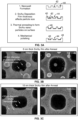
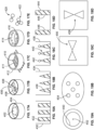
- Figure 2 is a diagrammatical representation of several examples of plasmonic nanostructures in nanowells 26.
- nanostructures include, for example, bowtie nanoantennae 28, nanospheres 34, nanopyramids, nanoshells, nanorods, nanowires, nanorings, nanoplugs 30, nanogratings 32 and the like.
- Preformed dimers 36 and trimers 28 of nanoparticles can also be loaded into wells and have the advantage of precisely controlling nanoparticle spacing.
- nanostructures can either be fabricated on a surface or pre-formed and then loaded into nanowells.
- examples of such structures include plasmonic nanoplugs fabricated at the bottom of nanowells, bowtie and cavity antennas in nanowells, metal nanogratings on which nanowells could be formed, nanoparticles reflowed in nanowells or a combination of some or all of the above.
- One example would be a metal nanoplug in a nanowell with nanoparticles on the walls formed through a simple electron beam evaporation process.
- Nanoparticle constructs (dimers, n-mers) formed using DNA origamis or linker molecules such as cucurbit[n]urils are also attractive for loading into wells. Such methods allow for precise subnanometer control over nanoparticle spacings and can be formed on a large scale using bottom up self-assembly. Examples of these structures are shown in Figure 2 .
- the spacing between any two nanoparticles on a surface can be any distance.
- the spacing can be a multiple of a wavelength of incident light energy, such as a particular emission or excitation wavelength in fluorescence spectroscopy.
- the spacing can be, for example, 1 ⁇ , 2 ⁇ , 3 ⁇ , 4 ⁇ or another multiple of a chosen wavelength ( ⁇ ) of incident light energy.
- ⁇ chosen wavelength
- the spacing between nanoparticles can be about 532 nm (1 ⁇ ), about 1064 nm (2 ⁇ ), or another multiple of the emission wavelength.
- the spacing can be a fraction of a wavelength of incident light energy, such as a particular emission or excitation wavelength in fluorescence spectroscopy.
- the spacing can be, for example, 1 ⁇ , 1 ⁇ 2 ⁇ , 1/3 ⁇ , 1/4 ⁇ or another multiple of a chosen wavelength of incident light energy.
- an emission wavelength of ( ⁇ ) 532 nm the spacing between nanoparticles can be about 532 nm (1 ⁇ ), 266 nm (1/2 ⁇ ), 133 nm (1/3 ⁇ ) or another fraction of the emission wavelength.
- plasmonic nanostructure or “nanoplasmonic structure” are used interchangeably herein and refer to any independent structure exhibiting plasmon resonance characteristic of the structure, including (but not limited to) both nanostructures, nanoparticles and combinations or associations of nanoparticles.
- nanoantenna refers to a nanoparticle or nanostructure that acts to amplify electromagnetic energy, such as light energy.
- a nanoantenna does not necessarily exhibit plasmon resonance characteristics.
- a nanoantenna does not substantially comprise a plasmon resonant material.
- nanoantennas are presented which are made of a non-metal material but which exhibits amplification characteristics of electromagnetic energy. Nanoparticles presented herein can be of any suitable shape and size so as to produce the desired energy amplification.
- nanoantennas include, for example, bowtie nanoantennae, nanospheres, nanopyramids, nanoshells, nanorods, nanowires, nanorings, nanoplugs, nanogratings and the like. It will be appreciated that any of a number of known methods can be suitable for fabrication and/or deposition of nanoantenna on a solid support (or substrate body). Methods for fabrication of nanoantenna are known in the art and include, for example, the methods described herein for nanoparticle fabrication and deposition.
- the nanoparticles can comprise any material suitable for use in the methods and compositions described herein, for example, any type of material exhibiting surface plasmon resonance (SPR).
- the nanoparticle comprises a plasmon resonant material.
- examples include, but are not limited to, metal nanoparticles.
- the nanoparticles can comprise a metal such as one or more of Gold (Au), Silver (Ag), Tin (Sn) Rhodium (Rh), Ruthenium (Ru), Palladium (Pd), Osmium (Os), Iridium (Ir), Platinum (Pt), Titanium (Ti) and Aluminum (Al), Chromium (Cr), Copper (Cu), or any other suitable metal.
- the nanoparticles can be formed from a single material such as, for example a single metal. Additionally or alternatively, the nanoparticles can be formed from a combination of two or more different materials, such as, for example, two or more metals.
- the nanoparticles can comprise a metal/metal mixture such as Sn/Au or Ag/Au. Alternatively or additionally, vertical layered nanoparticles, such as multilayer structures of the metal-insulator-metal type may be applied. Examples include Silicon (Si).
- the nanoparticles may include p-type doped silicon and n-type doped silicon. Gallium arsenide may also be used.
- Nanoparticles on a solid support can be performed using any one of a number of methods known in the art.
- Nanoparticles can be formed using bottom-up self-assembly of plasmonic nanostructures and nano-antennae on the sequencing substrate.
- any one of a number of methods for deposition of layers of a material can be used, such as those described by Gaspar et al. (Scientific Reports, 2013, 3, 1469 ).
- nanoparticles 10 can be pre-formed and mixed in a colloid-like composition with a gel material 12, which is deposited on a surface 14 of a solid support 16.
- a seeding operation may occur in which nucleic acids 18 (or other biomoleclues) are immobilized to the gel material 12.
- a clustering operation may be performed to form a cluster 20 of the nucleic acids 18.
- the clusters may be generated, for example, through bridge amplification.
- nanoparticles can be first deposited on a surface followed by deposition of a gel material over the nanoparticles.
- a gel material can be deposited on a surface and nanoparticles are deposited over the gel material.
- the nanoparticles are formed in a well (or concave feature or reaction cavity) of a solid surface.
- a film of starting material 40 such as Sn/Au can be deposited on a solid surface 42 containing nanowells 44, followed by thermal annealing.
- thermal annealing can be utilized to promote formation of nanoparticles 46 as the film coalesces into discrete particles.
- nanoparticle size can be a function of the starting film thickness.
- a further polishing step following the thermal anneal can result in nanoparticles 46 only in the wells while leaving the interstitial regions 48 substantially void of nanoparticles.
- Figure 5 is a further example of deposition of a layer of Sn/Au followed by thermal annealing.
- the SEM image of nanoparticles shown in Figure 5 demonstrates that nanoparticles are seen in every nanowell. Nanoparticles in interstitial regions can be removed through, for example, chemical and/or mechanical polishing. A distribution of nanoparticle sizes is observed in each nanowell enabling broad spectrum fluorescence enhancement.
- a nanostructures such as a nanoring can be formed along the wall of wells (or concave features or reaction cavities) on a surface.
- the nanostructures can be fabricated using any one of a number of methodologies known in the art.
- Figure 4 shows a schematic and SEM images showing formation of nanorings 50 in nanowells 52.
- Au can be deposited using sputtered deposition of a layer 54 of a material such as Au.
- conformal deposition of a ⁇ 65 nm Au layer was followed by a reactive ion etch (RIE) process. The remaining Au layer was located along the walls of the nanowells, forming nanorings 52 in each of the nanowells.
- RIE reactive ion etch
- the term "surface” is intended to mean an external part or external layer of a solid support or gel material.
- the surface can be in contact with another material such as a gas, liquid, gel, polymer, organic polymer, second surface of a similar or different material, metal, or coat.
- the surface, or regions thereof, can be substantially flat.
- the surface can have surface features such as wells, pits, channels, ridges, raised regions, pegs, posts or the like.
- solid support refers to a rigid substrate that is insoluble in aqueous liquid.
- the solid support may also be referred to as a substrate body.
- the substrate of the solid support can be non-porous or porous.
- the substrate can optionally be capable of taking up a liquid (e.g. due to porosity) but will typically be sufficiently rigid that the substrate does not swell substantially when taking up the liquid and does not contract substantially when the liquid is removed by drying.
- a nonporous solid support is generally impermeable to liquids or gases.
- Solid supports can optionally be inert to a chemistry that is used to modify a gel.
- a solid support can be inert to chemistry used to attach analytes, such as nucleic acids, to gels in a method set forth herein.
- exemplary solid supports include, but are not limited to, glass and modified or functionalized glass, plastics (including acrylics, polystyrene and copolymers of styrene and other materials, polypropylene, polyethylene, polybutylene, polyurethanes, Teflon TM , cyclic olefins, polyimides etc.), nylon, ceramics, resins, Zeonor, silica or silica-based materials including silicon and modified silicon, carbon, metals, inorganic glasses, optical fiber bundles, and polymers.
- a solid support having a patterned or structured substrate can comprise a patterned gel array, as described in U.S. Ser. No. 13/787,396 ( U.S. Patent Appl. Publ. 2014/0243224 A1 ).
- a structured substrate can be made by patterning a solid support material with wells (e.g. microwells or nanowells), coating the patterned support with a gel material (e.g.
- PAZAM PAZAM, SFA or chemically modified variants thereof, such as the azidolyzed version of SFA (azido-SFA)) and polishing the gel coated support, for example via chemical or mechanical polishing, thereby retaining gel in the wells but removing or inactivating substantially all of the gel from the interstitial regions on the surface of the structured substrate between the wells.
- Primer nucleic acids can be attached to gel material.
- a solution of target nucleic acids e.g. a fragmented human genome
- Amplification of the target nucleic acids will be confined to the wells since absence or inactivity of gel in the interstitial regions prevents outward migration of the growing nucleic acid colony.
- the process is conveniently manufacturable, being scalable and utilizing conventional micro- or nano-fabrication methods.
- a solid support used in a structured substrate set forth herein can be made from any of a variety of materials set forth herein, for example, above in the definitions, below in the examples or immediately following.
- a particularly useful material is glass.
- suitable substrate materials may include polymeric materials, plastics, silicon, quartz (fused silica), borofloat glass, silica, silica-based materials, carbon, metals, an optical fiber or optical fiber bundles, sapphire, or plastic materials such as COCs and epoxies.
- the particular material can be selected based on properties desired for a particular use. For example, materials that are transparent to a desired wavelength of radiation are useful for analytical techniques that will utilize radiation of the desired wavelength, such as one or more of the techniques set forth herein.
- a material that does not pass radiation of a certain wavelength e.g. being opaque, absorptive or reflective.
- This can be useful for formation of a mask to be used during manufacture of the structured substrate, such as a method set forth herein; or to be used for a chemical reaction or analytical detection carried out using the structured substrate, such as those set forth herein.
- Other properties of a material that can be exploited are inertness or reactivity to certain reagents used in a downstream process, such as those set forth herein; or ease of manipulation or low cost during a manufacturing process manufacture, such as those set forth herein. Further examples of materials that can be used in the structured substrates or methods of the present disclosure are described in US Ser. No. 13/661,524 and US Pat. App. Pub. No. 2012/0316086 A1 .
- Particularly useful solid supports for some embodiments are located within a flow cell apparatus.
- Exemplary flow cells, methods for their manufacture and methods for their use are described in US Pat. App. Publ. Nos. 2010/0111768 A1 or 2012-0270305 A1 ; or WO 05/065814 .
- Flow cells provide a convenient format for housing an array that is produced by the methods of the present disclosure and that is subjected to a sequencing-by-synthesis (SBS) or other technique that involves repeated delivery of reagents in cycles (e.g. synthesis techniques or detection techniques having repetitive or cyclic steps). Exemplary detection methods are set forth in further detail below.
- SBS sequencing-by-synthesis
- Exemplary detection methods are set forth in further detail below.
- a flow-cell or other vessel having multiple surfaces is used. Vessels having multiple surfaces can be used such that only a single surface has gel-containing concave features (e.g. wells). Alternatively two or more surfaces present in the vessel can have gel-containing concave features.
- One or more surfaces of a flow cell can be selectively detected. For example, opposing surfaces in the interior of a flow cell can be selectively addressed with focused radiation using methods known in the art such as confocal techniques.
- Useful confocal techniques and devices for selectively directing radiation to multiple surfaces of a vessel are described, for example, in US Pat. App. Pub. No. 2009/0272914 A1 or US Pat. No. 8,039,817 .
- gel material is intended to mean a semi-rigid material that is permeable to liquids and gases. Typically, gel material can swell when liquid is taken up and can contract when liquid is removed by drying.
- Exemplary gels include, but are not limited to those having a colloidal structure, such as agarose; polymer mesh structure, such as gelatin; or cross-linked polymer structure, such as polyacrylamide, SFA (see, for example, US Pat. App. Pub. No. 2011/0059865 A1 ) or PAZAM (see, for example, US Prov. Pat. App. Ser. No. 61/753,833 or U.S. Patent Appl. Publ. No. 2011/0059865 A1 ).
- Particularly useful gel material will conform to the shape of a well or other concave feature where it resides.
- Some useful gel materials can both (a) conform to the shape of the well or other concave feature where it resides and (b) have a volume that does not substantially exceed the volume of the well or concave feature where it resides.
- an interstitial region refers to an area in a substrate or on a surface that separates other areas of the substrate or surface.
- an interstitial region can separate one well (or concave feature) of an array from another well (or concave feature) of the array.
- the two regions that are separated from each other can be discrete, lacking contact with each other.
- an interstitial region can separate a first portion of a feature from a second portion of a feature.
- the interstitial region is continuous whereas the features are discrete, for example, as is the case for an array of wells in an otherwise continuous surface.
- the separation provided by an interstitial region can be partial or full separation.
- Interstitial regions will typically have a surface material that differs from the surface material of the features on the surface.
- features of an array can have an amount or concentration of gel material or analytes that exceeds the amount or concentration present at the interstitial regions.
- the gel material or analytes may not be present at the interstitial regions.
- the interstitial region can be substantially devoid of nanostructures by polishing the solid support, for example via chemical or mechanical polishing, thereby retaining nanostructures in the wells but removing or inactivating substantially all of the nanostructures from the interstitial regions on the surface of the structured substrate between the wells.
- Mechanical polishing can be carried out by applying abrasive forces to the surface of the solid support. Exemplary methods include abrasion with a slurry of beads, wiping with a sheet or cloth, scraping or the like. It will be understood that beads used for polishing or other uses set forth herein can be, but need not be, spherical. Rather beads can have irregular shapes, polygonal shapes, ovoid shapes, elongated shapes, cylindrical shapes etc.
- the surface of the beads can be smooth or rough. Any of a variety of particles can be useful as beads for the methods and compositions set forth herein.
- polishing includes using a lintless (cleanroom grade) wipe coated with a 3 ⁇ m silica bead slurry (10%w/v in water) to remove interstitial nanostructures.
- a polishing wheel/grinder can also be used with this slurry.
- Mechanical polishing can also be achieved using a fluid jet or gas (e.g. air or inert gas such as Argon or Nitrogen) jet to remove gel from interstitial regions.
- a fluid jet or gas e.g. air or inert gas such as Argon or Nitrogen
- a library when used in reference to analytes, refers to a collection of analytes having different chemical compositions.
- the analytes in a library will be different species having a common feature or characteristic of a genera or class, but otherwise differing in some way.
- a library can include nucleic acid species that differ in nucleotide sequence, but that are similar with respect to having a sugar-phosphate backbone.
- nucleic acid and “nucleotide” are intended to be consistent with their use in the art and to include naturally occurring species or functional analogs thereof. Particularly useful functional analogs of nucleic acids are capable of hybridizing to a nucleic acid in a sequence specific fashion or capable of being used as a template for replication of a particular nucleotide sequence.
- Naturally occurring nucleic acids generally have a backbone containing phosphodiester bonds. An analog structure can have an alternate backbone linkage including any of a variety of those known in the art.
- Naturally occurring nucleic acids generally have a deoxyribose sugar (e.g. found in deoxyribonucleic acid (DNA)) or a ribose sugar (e.g.
- a nucleic acid can contain nucleotides having any of a variety of analogs of these sugar moieties that are known in the art.
- a nucleic acid can include native or non-native nucleotides.
- a native deoxyribonucleic acid can have one or more bases selected from the group consisting of adenine, thymine, cytosine or guanine and a ribonucleic acid can have one or more bases selected from the group consisting of uracil, adenine, cytosine or guanine.
- Useful non-native bases that can be included in a nucleic acid or nucleotide are known in the art.
- probe or "target,” when used in reference to a nucleic acid, are intended as semantic identifiers for the nucleic acid in the context of a method or composition set forth herein and does not necessarily limit the structure or function of the nucleic acid beyond what is otherwise explicitly indicated.
- probe and target can be similarly applied to other analytes such as proteins, small molecules, cells or the like.
- the terms “coat” and “coating” and like terms when used as a verb, are intended to mean providing a layer or covering on a surface. At least a portion of the surface can be provided with a layer or cover. In some cases the entire surface can be provided with a layer or cover. In alternative cases only a portion of the surface will be provided with a layer or covering.
- the term "coat,” when used to describe the relationship between a surface and a material, is intended to mean that the material is present as a layer or cover on the surface.
- the material can seal the surface, for example, preventing contact of liquid or gas with the surface. However, the material need not form a seal.
- the material can be porous to liquid, gas, or one or more components carried in a liquid or gas.
- Exemplary materials that can coat a surface include, but are not limited to, a gel, polymer, organic polymer, liquid, metal, a second surface, plastic, silica, or gas.
- Structured substrates of the present disclosure that contain nucleic acid arrays can be used for any of a variety of purposes.
- a particularly desirable use for the nucleic acids is to serve as capture probes that hybridize to target nucleic acids having complementary sequences.
- the target nucleic acids once hybridized to the capture probes can be detected, for example, via a label recruited to the capture probe.
- Methods for detection of target nucleic acids via hybridization to capture probes are known in the art and include, for example, those described in US Pat. Nos.7,582,420 ; 6,890,741 ; 6,913,884 or 6,355,431 or US Pat. App. Pub. Nos. 2005/0053980 A1 ; 2009/0186349 A1 or 2005/0181440 A1 .
- a label can be recruited to a capture probe by virtue of hybridization of the capture probe to a target probe that bears the label.
- a label can be recruited to a capture probe by hybridizing a target probe to the capture probe such that the capture probe can be extended by ligation to a labeled oligonucleotide (e.g. via ligase activity) or by addition of a labeled nucleotide (e.g. via polymerase activity).
- a nucleic acid array can also be used in a sequencing procedure, such as a sequencing-by-synthesis (SBS) technique.
- SBS can be initiated by contacting the target nucleic acids with one or more labeled nucleotides, DNA polymerase, etc.
- Those features where a primer is extended using the target nucleic acid as template will incorporate a labeled nucleotide that can be detected.
- the labeled nucleotides can further include a reversible termination property that terminates further primer extension once a nucleotide has been added to a primer.
- a nucleotide analog having a reversible terminator moiety can be added to a primer such that subsequent extension cannot occur until a deblocking agent is delivered to remove the moiety.
- a deblocking reagent can be delivered to the flow cell (before or after detection occurs). Washes can be carried out between the various delivery steps. The cycle can then be repeated n times to extend the primer by n nucleotides, thereby detecting a sequence of length n.
- Pyrosequencing detects the release of inorganic pyrophosphate (PPi) as particular nucleotides are incorporated into a nascent nucleic acid strand ( Ronaghi, et al., Analytical Biochemistry 242(1), 84-9 (1996 ); Ronaghi, Genome Res. 11(1), 3-11 (2001 ); Ronaghi et al. Science 281(5375), 363 (1998 ); US Pat. Nos. 6,210,891 ; 6,258,568 and 6,274,320 ).
- PPi inorganic pyrophosphate
- pyrosequencing In pyrosequencing, released PPi can be detected by being converted to adenosine triphosphate (ATP) by ATP sulfurylase, and the resulting ATP can be detected via luciferase-produced photons.
- the sequencing reaction can be monitored via a luminescence detection system.
- Excitation radiation sources used for fluorescence based detection systems are not necessary for pyrosequencing procedures.
- Useful fluidic systems, detectors and procedures that can be used for application of pyrosequencing to arrays of the present disclosure are described, for example, in WIPO Pat. App. Ser. No. PCT/US11/57111 , US Pat. App. Pub. No. 2005/0191698 A1 , US Pat. No. 7,595,883 , and US Pat. No. 7,244,559 .
- Sequencing-by-ligation reactions are also useful including, for example, those described in Shendure et al. Science 309:1728-1732 (2005 ); US Pat. No. 5,599,675 ; and US Pat. No. 5,750,341 .
- Some embodiments can include sequencing-by-hybridization procedures as described, for example, in Bains et al., Journal of Theoretical Biology 135(3), 303-7 (1988 ); Drmanac et al., Nature Biotechnology 16, 54-58 (1998 ); Fodor et al., Science 251(4995), 767-773 (1995 ); and WO 1989/10977 .
- nucleic acids that are present in gel-containing wells are subjected to repeated cycles of oligonucleotide delivery and detection.
- Fluidic systems for SBS methods as set forth herein, or in references cited herein can be readily adapted for delivery of reagents for sequencing-by-ligation or sequencing-by-hybridization procedures.
- the oligonucleotides are fluorescently labeled and can be detected using fluorescence detectors similar to those described with regard to SBS procedures herein or in references cited herein.
- Some embodiments can utilize methods involving the real-time monitoring of DNA polymerase activity.
- nucleotide incorporations can be detected through fluorescence resonance energy transfer (FRET) interactions between a fluorophore-bearing polymerase and ⁇ -phosphate-labeled nucleotides, or with zeromode waveguides.
- FRET fluorescence resonance energy transfer
- Techniques and reagents for FRET-based sequencing are described, for example, in Levene et al. Science 299, 682-686 (2003 ); Lundquist et al. Opt. Lett. 33, 1026-1028 (2008 ); Korlach et al. Proc. Natl. Acad. Sci. USA 105, 1176-1181 (2008 ).
- RNA sequencing techniques can be carried out using sequencing methodologies known in the art such as those set forth above.
- Gene expression can also be detected or quantified using hybridization techniques carried out by direct hybridization to an array or using a multiplex assay, the products of which are detected on an array.
- An array of the present disclosure can also be used to determine genotypes for a genomic DNA sample from one or more individual. Exemplary methods for array-based expression and genotyping analysis that can be carried out on an array of the present disclosure are described in US Pat.
- a single nucleic acid whether a target nucleic acid or amplicon thereof, can be detected at each feature.
- a gel-containing well or other concave feature
- Any of a variety of single molecule detection techniques can be used including, for example, modifications of the ensemble detection techniques set forth above to detect the sites at increased resolution or using more sensitive labels.
- Other examples of single molecule detection methods that can be used are set forth in US Pat. App. Pub. No. 2011/0312529 A1 ; US Ser. No. 61/578,684 ; and US Ser. No. 61/540,714 .
- the term "well” refers to a discrete concave feature in a solid support having a surface opening that is completely surrounded by interstitial region(s) of the surface.
- Wells can have any of a variety of shapes at their opening in a surface including but not limited to round, elliptical, square, polygonal, star shaped (with any number of vertices) etc.
- the cross section of a well taken orthogonally with the surface can be curved, square, polygonal, hyperbolic, conical, angular, etc.
- concave feature when used in reference to a solid support, refers to a recess or indentation in the solid support.
- exemplary concave features include, but are not limited to, a well, pit, hole, depression, channel, or trough.
- a concave feature can optionally have a curved cross section (in the dimension orthogonal to the surface of the solid support); however, a cross section with one or more linear sections, angles or corners is also possible. Cross sections with combinations of curved and linear sections are also possible.
- a concave feature need not pass completely through the solid support, for example, instead having a bottom surface or point in the substrate.
- This example describes the use of localized surface plasmon resonance (SPR) to increase the fluorescence intensity of amplified DNA on a solid surface (DNA "clusters").
- SPR surface plasmon resonance
- results are shown on unpatterned glass surface coated with silane-free acrylamide (SFA) that was spiked with Au nanoparticles. DNA clusters were then amplified on this surface.
- SFA silane-free acrylamide
- FIG. 1 An example workflow is presented in Figure 1 .
- SFA spiked with Au nanoparticles 10 is coated on a glass surface 14 and amplification primers (not shown) are grafted to the SFA.
- template DNA 18 is seeded onto the surface or gel material. Seeded template DNA 18 is then amplified on the surface as shown in the third panel, forming clusters 20 of amplified DNA, with some clusters formed directly over Au nanoparticles 10, while other clusters are formed on a portion of the surface that does not contain Au nanoparticles.
- fluorescence 22 from each cluster is detected during a sequencing by synthesis reaction. Proximity to Au nanoparticles results in enhanced fluorescence compared to the signal emitted from clusters that are not in proximity to Au nanoparticles.
- Lanes 1, 2 were control lanes (no nanoparticles).
- Lanes 3-6 were spiked with a 50 nM concentration of 6nm spherical Au nanoparticles. The high Au NP concentration prevented polymerization of the in-situ coated SFA in these lanes, preventing grafting.
- Lanes 7, 8 were coated with SFA spiked with 10 nM concentration Au nanoparticles. Higher fluorescence intensities were seen from Lanes 7, 8 relative to the control lanes. Sequencing results indicated that the intensity for base A increased ⁇ 27% relative to the control lanes. A -24% increase in intensity was observed on average for all 4 bases relative to the control lanes.
- Plasmonic nanostructures can also be combined with patterned nanowell substrates for enhanced fluorescence.
- fluorescence enhancement was achieved using nanoparticles in nanowells.
- Nanoparticles were formed in nanowells using a novel Sn/Au reflow approach. As illustrated in Figure 3A , a uniform film of Sn/Au was first coated on the nanowell substrate followed by a thermal annealing process at 400°C which resulted in the reflow of the film into small nanoparticles (see Figures 3B and 3C ). By controlling initial film thickness, nanoparticle size was manipulated. Examples of this are shown in Figures 3B and 3C for starting film thicknesses of 6 nm and 10 nm, respectively, resulting in >50 nm diameter particles and ⁇ 30 nm particles respectively.
- nanoparticle formation Following nanoparticle formation, mechanical polishing was used to remove nanoparticles from the interstitial regions resulting in only particles in wells.
- loading efficiency resulting from the fact that nanoparticles are loaded into every well.
- a further advantage of this technique is that the broad distribution of nanoparticle sizes gives broad spectrum fluorescence enhancement compared to enhancement at a small range of wavelengths as typically achieved using a single nanoparticle size.
- Figures 6 and 7 set forth exemplary results.
- Figure 6 sets forth sequencing results using isothermal amplification followed by SBS sequencing. Sequencing by synthesis was conducted for 26 cycles and compared with a control region that was void of Sn/Au deposition. Cluster intensity per cycle for each of four fluorescently labeled bases was measured as a function of Sn/Au particle thickness.
- the patterned substrates had ⁇ 500 nm diameter wells with a pitch of 850 nm. Different Sn/Au thicknesses were deposited on different regions of a single flowcell and then annealed. Combining different film thicknesses and a control region in each lane allowed for a direct comparison of intensities from different regions of the same flow cell, thereby decoupling chemistry variations.
- Clusters were seen in all 3 regions of each lane, confirming reflowed Sn/Au nanoparticles of various size support clustering.
- a comparison of normalized cluster intensity enhancement (over control) in these regions at cycle 1 and cycle 26 is shown in Figure 7 .
- the top line illustrates the relationship between intensity and cycle number for 6nm particles
- the middle line illustrates the relationship between intensity and cycle number for glass
- the bottom line illustrates the relationship between intensity and cycle number for 10nm particles.
- nanostructures utilize one or more nanostructures to amplify electromagnetic energy at a reaction site.
- the plurality of nanostructures may be referred to as an ensemble amplifier.
- the terms “nanostructure” and “nanoparticle” are used interchangeably to refer to a structure having a greatest dimension (e.g, height, width, diameter) in the range of about 1 nm to about 1000 nm, including any integer or non-integer value between 1 nm and 1000 nm.
- the nanoparticle is a metallic particle or a silicon particle.
- the nanoparticle core is a spherical or nearly spherical particle of 20-200 nm in diameter. In some embodiments the range is about 1 nm to about 50 nm (for example about 1, 2, 3, 4, 5, 6, 7, 8, 9, 10, 11, 12, 13, 14, 15, 16, 17, 18, 19, 20, 21, 22, 23, 24, 25, 26, 27, 28, 29, 30, 31, 32, 33, 34, 35, 36, 37, 38, 39, 40, 41, 42, 43, 44, 45, 46, 47, 48, 49, or 50 nm).
- Anisotropic nanostructures may have a length and a width or, for some embodiments, a diameter.
- the length of the anisotropic nanostructure is the greatest dimension of the nanostructure.
- the length of an anisotropic nanoparticle is a dimension parallel to the plane of the aperture in which the nanoparticle was produced.
- the length of an anisotropic nanoparticle is the dimension perpendicular to the plane of the aperture in which the nanoparticle was produced.
- the nanostructure may have a width or diameter in the range of about 50 nm to about 750 nm.
- the nanostructure has a width or diameter of about 350 nm or less. In other embodiments, the nanoparticle has a width or diameter of 250 nm or less and in some embodiments, a width or diameter of 100 nm or less. In some embodiments, the width or diameter is between 15 nm to 300 nm.
- the nanoparticle has a length of about 10-750 nm.
- the nanostructures have a preselected shape and can be, for example a nanotube, a nanowire, nanosphere, or any shape comprising the above-described dimensions (e.g., triangular, square, rectangular, or polygonal shape in 2 dimensions, or cuboid, pyramidal, cylindrical, spherical, discoid, or hemispheric shapes in the 3 dimensions).
- Some examples of nanostructures include, for example, bowtie nanoantennae, nanospheres, nanopyramids, nanoshells, nanorods, nanowires, nanorings, nanoplugs, nanogratings and the like. Preformed dimers and trimers of nanostructures can also be loaded into wells and have the advantage of precisely controlling nanoparticle spacing.
- the nanostructures can either be fabricated on a surface or pre-formed and then loaded into reaction cavities, such as wells (e.g., nanowells).
- reaction cavities such as wells (e.g., nanowells).
- examples of such structures include plasmonic nanoplugs fabricated at the bottom of nanowells, bowtie and cavity antennas in nanowells, metal nanogratings on which nanowells could be formed, nanostructures reflowed in nanowells or a combination of some or all of the above.
- One example would be a metal nanoplug in a nanowell with nanostructures on the walls formed through an electron beam evaporation process.
- Ensemble amplifiers or constructs may also be positioned within the reaction cavities. Such methods allow for precise subnanometer control over nanostructure spacings and can be formed on a large scale using bottom up self-assembly.
- the spacing between any two nanostructures on a surface can be any distance.
- the spacing can be a multiple of a wavelength of incident light energy, such as a particular emission or excitation wavelength in fluorescence spectroscopy.
- the spacing can be, for example, 1 ⁇ , 2 ⁇ , 3 ⁇ , 4 ⁇ or another multiple of a chosen wavelength ( ⁇ ) of incident light energy.
- ⁇ chosen wavelength
- the spacing between nanostructures can be about 532 nm (1 ⁇ ), about 1064 nm (2 ⁇ ), or another multiple of the emission wavelength.
- the spacing can be a fraction of a wavelength of incident light energy, such as a particular emission or excitation wavelength in fluorescence spectroscopy.
- the spacing can be, for example, 1 ⁇ , 1 ⁇ 2 ⁇ , 1/3 ⁇ , 1/4 ⁇ or another multiple of a chosen wavelength of incident light energy.
- the spacing between nanostructures can be about 532 nm (1 ⁇ ), 266 nm (1/2 ⁇ ), 133 nm (1/3 ⁇ ) or another fraction of the emission wavelength.
- the nanostructures may be referred to as "plasmonic nanostructure” or “nanoplasmonic structure.” These terms may be used interchangeably and refer to any independent structure exhibiting plasmon resonance characteristic of the structure, including (but not limited to) both nanostructures, nanostructures and combinations or associations of nanostructures.
- nanoantenna includes a nanostructure or a plurality of nanostructures (or ensemble amplifier) that acts to amplify electromagnetic energy, such as light energy.
- a nanoantenna (or ensemble amplifier) does not necessarily exhibit plasmon resonance characteristics.
- a nanoantenna does not substantially comprise a plasmon resonant material.
- nanoantennas are presented which are made of a non-metal material but which exhibits amplification characteristics of electromagnetic energy. Nanostructures presented herein can be of any suitable shape and size so as to produce the desired energy amplification.
- nanoantennas include, for example, bowtie nanoantennae, nanospheres, nanopyramids, nanoshells, nanorods, nanowires, nanorings, nanoplugs, nanogratings and the like. It will be appreciated that any of a number of known methods can be suitable for fabrication and/or deposition of nanoantenna on a solid support. Methods for fabrication of nanoantenna are known in the art and include, for example, the methods described herein for nanoparticle fabrication and deposition.
- the nanostructures can comprise any material suitable for use in the methods and compositions described herein, for example, any type of material exhibiting surface plasmon resonance (SPR).
- the nanoparticle comprises a plasmon resonant material.
- examples include, but are not limited to, metal nanostructures.
- the nanostructures can comprise a metal such as one or more of Gold (Au), Silver (Ag), Tin (Sn) Rhodium (Rh), Ruthenium (Ru), Palladium (Pd), Osmium (Os), Iridium (Ir), Platinum (Pt), Titanium (Ti) and Aluminum (Al), Chromium (Cr), Copper (Cu), or any other suitable metal.
- the nanostructures can be formed from a single material such as, for example a single metal. Additionally or alternatively, the nanostructures can be formed from a combination of two or more different materials, such as, for example, two or more metals.
- the nanostructures can comprise a metal/metal mixture such as Sn/Au or Ag/Au.
- vertical layered nanostructures, such as multilayer structures of the metal-insulator-metal type may be applied. Examples include p-type doped silicon, n-type doped silicon, and gallium arsenide.
- the nanostructures may be formed from a polymer that is coated by a plasmon resonant material and/or a metallic material.
- Nanostructures on a solid support can be performed using any one of a number of methods known in the art.
- Nanostructures can be formed using bottom-up self-assembly of plasmonic nanostructures and nano-antennae on the sequencing substrate.
- any one of a number of methods for deposition of layers of a material can be used, such as those described by Gaspar et al. (Scientific Reports, 2013, 3, 1469 ),.
- Layer-fabricating processes that may be used to form the nanostructures include photolithography, etching, sputtering, evaporation, casting (e.g., spin coating), chemical vapor deposition, electrodeposition, epitaxy, thermal oxidation, physical vapor deposition, and the like.
- the nanostructures may be formed using a shadow technique.
- the nanostructures may be formed using nanolithography, such as nanoimprint lithography (NIL).
- NIL nanoimprint lithography
- the nanostructures can be pre-formed and mixed in a colloid-like composition with a gel material, which is deposited on a surface.
- nanostructures can be first deposited on a surface followed by deposition of a gel material over the nanostructures.
- a gel material can be deposited on a surface and nanostructures are deposited over the gel material.
- the nanostructures are formed in a well (or concave feature) of a solid surface.
- a film of starting material such as Sn/Au can be deposited on a solid surface containing nanowells, followed by thermal annealing.
- thermal annealing can be utilized to promote formation of nanostructures as the film coalesces into discrete particles.
- Nanoparticle size can be a function of the starting film thickness.
- a further polishing step following the thermal anneal can result in nanostructures only in the wells while leaving the interstitial regions substantially void of nanostructures. Nanostructures in interstitial regions can be removed through, for example, chemical and/or mechanical polishing. A distribution of nanoparticle sizes is observed in each nanowell enabling broad spectrum fluorescence enhancement.
- a nanostructures such as a nanoring can be formed along the wall of wells (or concave features) on a surface.
- the nanostructures can be fabricated using any one of a number of methodologies known in the art.
- Au can be deposited using sputtered deposition.
- conformal deposition of a ⁇ 65 nm Au layer may be followed by a reactive ion etch (RIE) process.
- RIE reactive ion etch
- excitation light and “light emissions” mean electromagnetic energy and are used to differentiate the source of the electromagnetic energy.
- Excitation light is generally provided from a light source (e.g., laser) that is positioned a distance away from the reaction site.
- the light source may be positioned outside of the reaction cavities.
- Light emissions are typically generated by an emitter within or at the reaction sites.
- the emitter may be, for example, a fluorophore.
- Particular embodiments may be configured to amplify electromagnetic energy at any wavelength between 300 nm to 750 nm (e.g., 300 nm, 301 nm, 302 nm, 303 nm, 304 nm, 305 nm, 306 nm, 307 nm, 308 nm ...745 nm, 746 nm, 747 nm, 748 nm, 749 nm, and 750 nm).
- the term “wavelength” shall not be limited to a single wavelength unless expressly stated to constitute "a single wavelength” or "only one wavelength”.
- wavelength shall encompass a narrow range of wavelengths located about a desired or target wavelength (e.g., 532 nm ⁇ 10 nm, 532 nm ⁇ 5 nm, 660 nm ⁇ 10 nm, 660 nm ⁇ 5 nm).
- the nanostructures of each ensemble amplifier may be configured relative to one another to amplify the electromagnetic energy in a designated manner. For example, a distance that separates the nanostructures of a corresponding ensemble amplifier may be based on the electromagnetic energy that is desired to be amplified.
- the nanostructures of the ensemble amplifier may be configured for a particular wavelength (e.g., narrow band of wavelengths). For example, one or more embodiments may be configured to amplify electromagnetic energy having a wavelength of 532 nm. One or more embodiments may be configured to amplify electromagnetic energy having a wavelength of 660 nm.
- the ensemble amplifiers may be capable of amplifying multiple wavelengths or broader ranges of wavelengths.
- the ensemble amplifier has a polarized configuration such that a response from the reaction site is based on a polarization of the electromagnetic energy.
- the ensemble amplifier may be configured to preferentially respond to electromagnetic energy having one or more predetermined polarizations.
- the light emissions may have a signal intensity that is larger than the signal intensity of the light emissions if the electromagnetic energy did not have the predetermined polarization.
- the ensemble amplifier when the ensemble amplifier is illuminated by electromagnetic energy having a predetermined polarization, the light emissions may have a signal intensity that is X.
- the ensemble amplifier may have a dipole moment that is essentially parallel to the electromagnetic energy with the predetermined polarization.
- substantially parallel may be +/- 30° from being parallel to the dipole moment.
- substantially parallel may be +/- 25° from being parallel to the dipole moment or +/- 20° from being parallel to the dipole moment.
- essentially parallel may be +/-15° from being parallel to the dipole moment or +/- 10° from being parallel to the dipole moment.
- essentially parallel may be +/- 8° from being parallel to the dipole moment, +/- 5° from being parallel to the dipole moment, or +/- 3° from being parallel to the dipole moment.
- the light emissions may have a signal intensity that is 0.4X or less (40% or less) than the signal intensity when the dipole moment is essentially parallel to the electromagnetic energy.
- the ensemble amplifier may have a dipole moment that is essentially perpendicular to the electromagnetic energy with the predetermined polarization.
- substantially perpendicular may be +/- 30° from being perpendicular (90°) to the dipole moment. In some embodiments, substantially perpendicular may be +/- 25° from being perpendicular to the dipole moment or +/- 20° from being perpendicular to the dipole moment.
- essentially perpendicular may be +/- 15° from being perpendicular to the dipole moment or +/- 10° from being perpendicular to the dipole moment. In more particular embodiments, essentially perpendicular may be +/- 8° from being perpendicular to the dipole moment, +/- 5° from being perpendicular to the dipole moment, or +/- 3° from being perpendicular to the dipole moment.
- FIG 10 is a cross-section of a portion of a structured substrate 100 formed in accordance with an embodiment.
- the structured substrate 100 includes a substrate body 102, which may also be referred to as a solid support.
- the substrate body (or solid support) 102 has an active side 104.
- the active side 104 includes a plurality of reaction sites 106 and a side surface 105 that extends between the reaction sites 106.
- the reaction sites 106 are reaction cavities or wells (e.g., nanowells). Accordingly, the reaction sites 106 will be hereinafter referred to as reaction cavities 106, but it is understood that other embodiments may include reaction sites.
- the reaction cavities 106 may have similar dimensions the nanowells described herein.
- the reaction cavities 106 may have a diameter or width measured along a lateral axis 191.
- the diameter or width of the reaction cavities may be less than 5000 nm.
- the diameter or width of the reaction cavities is less than 4000 nm, less than 3000 nm, less than 2000 nm, or less than 1000 nm.
- the diameter or width of the reaction cavities is less than 900 nm, less than 800 nm, less than 700 nm, or less than 600 nm.
- the diameter or width of the reaction cavities is less than 550 nm, less than 500 nm, less than 450 nm, or less than 400 nm.
- the diameter or width of the reaction cavities is less than 350 nm, less than 300 nm, less than 250 nm, less than 200 nm, less than 150 nm, or less than 100 nm.
- Reaction sites described herein may have similar diameters or widths.
- the reaction cavities 106 are spaced apart from each other by interstitial regions 118 of the substrate body 102.
- the interstitial regions 118 are areas along the active side 104 or portions of the substrate body 102 that separate the reaction cavities 106 from one another.
- the side surface 105 extends along the interstitial regions 118.
- the plurality of reaction cavities 106 form a dense array of reaction sites 106 such that adjacent reaction cavities 106 are separated, for example, by less than 1000 nm. In more particular embodiments, the adjacent reaction cavities 106 may be separated by less than 900 nm, less than 800 nm, less than 700 nm, or less than 600 nm.
- the adjacent reaction cavities 106 may be separated by less than 500 nm, less than 400 nm, less than 300 nm, or less than 200 nm. In more particular embodiments, the adjacent reaction cavities 106 may be separated by less than 150 nm, less than 100 nm, or less than 50 nm. Reaction sites described herein may have similar separation distances. In some embodiments, a center-to-center spacing 119 between adjacent reaction cavities 106 may be less than 1000 nm. In more particular embodiments, the center-to-center spacing 119 may be less than 700 nm, less than 600 nm, less than 500 nm, or less than 450 nm.
- the center-to-center spacing 119 may be less than 400 nm, less than 350 nm, less than 300 nm, less than 250 nm, or less than 200 nm. Reaction sites described herein may have center-to-center spacings.
- the interstitial regions 118 form a continuous, planar side surface 105, but the interstitial regions 118 may include non-planar surfaces in other embodiments.
- the interstitial regions 118 may include a surface material that differs from the material of the reaction cavities 106 and may functionally isolate the reaction cavities 106 from one another. In the illustrated embodiment, only two reaction cavities 106 are shown along the active side 104. It should be understood, however, that the reaction cavities 106 may be part of an array of reaction sites that may include hundreds, thousands, or millions of reaction cavities (or sites).
- the reaction cavities 106 are typically concave features that form a depression or indentation along the active side 104.
- the reaction cavities 106 may be, for example, wells, pits, channels, recesses, and the like. However, it should be understood that other embodiments may include reaction sites that are not located within cavities. For example, the reaction sites may be distributed along a planar surface. Such embodiments are described in U.S. Provisional Application No. 61/920,244 .
- the substrate body 102 may be formed from one or more stacked layers.
- the substrate body 102 includes a base layer 112 and a cavity layer 114.
- the base layer 112 may be, for example, a glass (SiO 2 ) wafer.
- the cavity layer 114 may be a polymer.
- the substrate body 102 may include other layers in alternative embodiments.
- each layer is not limited to a single continuous body of material unless otherwise noted.
- each layer may be formed form multiple sub-layers of the same or different materials.
- each layer may include one or more features of different materials located therein or extending therethrough.
- the different layers may be formed using known layer-fabricating processes, such as photolithography, etching, sputtering, evaporation, casting (e.g., spin coating), chemical vapor deposition, electrodeposition, epitaxy, thermal oxidation, physical vapor deposition, and the like.
- One or more layers may also be formed using nanolithography, such as nanoimprint lithography (NIL).
- NIL nanoimprint lithography
- working substrate includes one or more stacked layers in which at least one of the layers is being processed to form a structured substrate from the working substrate.
- the working substrate may form a solid support or substrate body that is configured to receive one or more other elements to form the structured substrate.
- the working substrate may receive nanoparticles and/or an organic material (e.g., gel material) to form a structured substrate.
- a reaction cavity has a cross section that is taken perpendicular to the active side 104.
- the cross-section may include curved sections, linear sections, angles, corners.
- a reaction cavity need not pass completely through one or more layers.
- each of the reaction cavities 106 has at least one sidewall 124 that extends between the active side 104 and a bottom surface 126 of the reaction cavity 106. Both the sidewall 124 and the bottom surface 126 are defined by the cavity layer 114.
- the base layer 112 (or other layer) may define the bottom 126 of the reaction cavity 106.
- the reaction cavities 106 open to the active side 104 such that the reaction cavities 106 are accessible along the active side 104.
- the reaction cavities 106 may be capable of receiving gel material and/or fluid along the active side 104 during manufacture of the structured substrate 100 or when the structured substrate 100 is used during analysis.
- the active side 104 may also receive an excitation light 108 from a light source (not shown) and/or face an optical component (not shown), such as an objective lens, that detects light emissions 110 from the reaction cavities.
- Each of the reaction cavities 106 may include at least one nanostructure 116.
- the interstitial regions 118 may be substantially devoid of nanostructures.
- each of the reaction cavities 106 includes a plurality of nanostructures 116.
- the plurality of nanostructures 116 may form an ensemble of nanostructures, which is hereinafter referred to as an ensemble amplifier 120.
- the ensemble amplifier 120 is positioned within each of the reaction cavities 106 and is configured to at least one of amplify electromagnetic energy that propagates into the corresponding reaction cavity or amplify electromagnetic energy that is generated within the corresponding reaction cavity.
- an “ensemble of nanostructures” or “ensemble amplifier” includes a plurality of nanostructures that are configured to at least one of amplify electromagnetic energy that is incident on the discrete site (e.g., reaction cavity) or amplify electromagnetic energy that is generated at the discrete site.
- the electromagnetic energy may be the excitation light 108 that propagates from an exterior environment and into a reaction cavity 106, wherein the excitation light is absorbed by an emitter (e.g., fluorophore) that is associated with a biological substance.
- the electromagnetic energy may be light emissions 110 that are emitted from the biological substances.
- the fluorophores may emit the electromagnetic energy (e.g., light emissions 110) that is then amplified by the ensemble 120 of nanostructures.
- the ensemble amplifier 120 may also be referred to as a nanoantenna, because the nanostructures collectively operate to amplify and transmit the light emissions 110 away from the reaction sites.
- An ensemble amplifier may include two or more nanostructures that operate in concert to amplify the electromagnetic energy. As described herein, in some embodiments, an ensemble amplifier may be configured to preferentially amplify a type of electromagnetic energy or, more specifically, electromagnetic energy having a predetermined wavelength. For example, an ensemble amplifier may have a greater amplification effect on light emissions than on excitation light or vice versa. Nonetheless, in some embodiments, an ensemble amplifier may amplify both the light emissions and the excitation light.
- each of the nanostructures may have one or more qualities such that the ensemble amplifier collectively operate to amplify the electromagnetic energy.
- the qualities may include, for example, a material composition of the nanostructure, a shape of the nanostructure, a size of the nanostructure, and a position of the nanostructure relative to other nanostructures in the ensemble.
- adjacent nanostructures 116 may have a distance 128 therebetween that is configured amplify electromagnetic energy that is confined therebetween.
- the resulting amplification in light emissions may be due to a combination of localized surface plasmon resonance and resonant energy transfer processes.
- the reaction cavities 106 may include an organic material 122 disposed within the reaction cavities 106.
- the organic material 122 may cover the nanostructures 116.
- the organic material 122 is configured to hold or immobilize a biomolecule within the corresponding reaction cavity.
- the biomolecule may be a nucleic acid.
- the organic material 122 includes a gel material, such as a hydrogel.
- gel material is intended to mean a semi-rigid material that is permeable to liquids and gases. Typically, gel material can swell when liquid is absorbed or received by the gel material and can contract when liquid is removed from the gel material (e.g., through drying).
- Exemplary gel materials include, but are not limited to those having a colloidal structure, such as agarose; polymer mesh structure, such as gelatin; or cross-linked polymer structure, such as polyacrylamide, SFA (see, for example, US Pat. App. Pub. No. 2011/0059865 A1 ) or PAZAM (see, for example, U.S. Prov. Pat.
- Particularly useful gel material will conform to the shape of a reaction cavity where it resides.
- Some useful gel materials can both (a) conform to the shape of the reaction cavity where it resides and (b) have a volume that does not substantially exceed the volume of the reaction cavity where it resides.
- the organic material 122 has a volume that is configured to accommodate only a single biomolecule (e.g., nucleic acid) such that steric exclusion prevents more than one biomolecule from being captured or seeding the reaction cavity.
- a single biomolecule e.g., nucleic acid
- Steric exclusion can be particularly useful for nucleic acids.
- reaction cavities can expose a surface of the organic material (e.g., gel material) having an area that is equivalent to or smaller than a diameter of the excluded volume of target nucleic acids that are to be seeded on the substrate.
- the excluded volume for a target nucleic acid and its diameter can be determined, for example, from the length of the target nucleic acid.
- a library of target nucleic acids can be delivered to reaction cavities that contain the gel material prior to initiation of an amplification process.
- target nucleic acids can be delivered to a structured substrate under conditions to seed the gel material in the substrate with the target nucleic acids.
- the structured substrate can optionally be washed to remove target nucleic acids that do not seed the gel material as well as any other materials that are unwanted for subsequent processing or use of the structured substrate.
- the area of the exposed gel material may be substantially greater than the diameter of the excluded volume of the target nucleic acids that are transported to the amplification sites.
- the area for the features can be sufficiently large that steric exclusion does not occur.
- the nanostructures 116 are formed along the base layer 112 such that the nanostructures 116 project from the base layer 112 and into the reaction cavities 106. In some embodiments, the nanostructures 116 extend through a portion of the cavity layer 114. In other embodiments, the bottom surface 126 may be defined by a portion of the base layer 122 such that the nanostructures 116 do not extend through the cavity layer 114. Also shown in Figure 10 , a flow cover 135 may be mounted to the substrate body 102.
- the light emissions may be generated in response to the excitation light 108.
- the excitation light 108 is not provided and, instead, the excitation light 108 is generated by emitters coupled to the biomolecule 129.
- a gain field 130 exists along one of the nanostructures 116 or between two or more nanostructures 116.
- the gain field 130 may represent a space where a high intensity electric field is created by the nanostructures 116 in response to excitation light and/or light emissions.
- the nanostructures 116 amplify the excitation light 108 such that the emitters are energized by the excitation light and provide a greater signal intensity for detection.
- the nanostructures 116 do not amplify the excitation light 108, but amplify the light emissions 110 such that the light emissions 110 provide a greater signal intensity for detection. In some applications, however, the nanostructures 116 may be capable of amplifying both the excitation light 108 and the light emissions 110 such that a greater intensity of the excitation light 108 is experienced by the emitters and a greater intensity of the light emissions 110 is provided by the emitters. Accordingly, embodiments set forth herein may provide a greater signal intensity that is easier to detect by imaging systems or devices compared to known systems that do not include nanostructures or ensemble amplifiers.
- the present application describes various methods for manufacturing or fabricating structured substrates that may be used to detect or analyze designated reactions. At least some of the methods are illustrated in the figures as a plurality of steps. However, it should be understood that embodiments are not limited to the steps illustrated in the figures. Steps may be omitted, steps may be modified, and/or other steps may be added. By way of example, although some embodiments described herein may include only two layers, other embodiments may include three, four, or more layers. Moreover, steps described herein may be combined, steps may be performed simultaneously, steps may be performed concurrently, steps may be split into multiple sub-steps, steps may be performed in a different order, or steps (or a series of steps) may be re-performed in an iterative fashion. In addition, although different methods are set forth herein, it should be understood that the different methods (or steps of the different methods) may be combined in other embodiments.
- the structured substrates may be formed using one or more processes that may, for example, be used to manufacture integrated circuits, during microfabrication, and/or to manufacture nanotechnology.
- Lithography e.g., photolithography
- NIL nanoimprint lithography
- Exemplary lithographic techniques or processes are described in greater detail in Marc J. Madou, Fundamentals of Microfabrication and Nanotechnology: Manufacturing Techniques for Microfabrication and Nanotechnology, Vol. II, 3rd Edition, Part I (pp. 2-145 ).
- One or more processes for fabricating structured substrates may also include subtractive techniques in which material is removed from a working substrate.
- Such processes include chemical techniques, such as dry chemical etching, physical/chemical etching, vapor phase etching, chemical machining (CM), anisotropic wet chemical etching, wet photoetching; electrochemical techniques, such as electrochemical etching (ECM), electrochemical grinding (ECG), photoelectrochemical etching; thermal techniques, such as laser machining, electron beam machining, electrical discharge machining (EDM); and mechanical techniques, such as physical dry etching, sputter etching, ion milling, water-jet machining (WJM), abrasive water-jet machining (AWJM), abrasive jet machining (AJM), abrasive grinding, electrolytic in-process dressing (ELID) grinding, ultrasonic drilling, focused ion beam (FIB) milling, and the like.
- chemical techniques such as dry chemical etching, physical/chemical etch
- One or more processes for fabricating structured substrates may also include additive techniques in which material is added to a working substrate.
- Such processes include physical vapor deposition (PVD), evaporation (e.g., thermal evaporation), sputtering, ion plating, ion cluster beam deposition, pulsed laser deposition, laser ablation deposition, molecular beam epitaxy, chemical vapor deposition (CVD) (e.g., atmospheric pressure CVD (APCVD), low pressure CVD (LPCVD), very low pressure CVD (VLPCVD), ultrahigh vacuum CVD (UHVCVD), metalorganic CVD (MOCVD), laser-assisted chemical vapor deposition (LCVD), plasma-enhanced CVD (PECVD), atomic layer deposition (ALD)), epitaxy (e.g., liquid-phase epitaxy, solid-phase epitaxy), anodization, thermal spray deposition, electroplating, implantation, diffusion, incorporation in the melt, thermal oxidation,
- FIG 11 is a flowchart illustrating a method 200 of manufacturing a structured substrate.
- the method 200 includes providing, at 202, a base layer (or working substrate) having a base side.
- the base layer may be only a single layer of material or include one or more sub-layers.
- the base side may have a planar surface that is configured to have another layer deposited directly thereon. However, it is contemplated that the base side may include non-planar features prior to being combined with other layers.
- the base layer includes a glass (SiO 2 ) wafer, but other materials may be used.
- the method 200 may also include forming, at 204, an array of nanostructures along the base side of the base layer.
- the forming, at 204 may include multiple processing steps.
- the forming, at 204 may include providing (e.g., through deposition, growing, or another additive technique) a feature layer along the base side of the base layer.
- the forming, at 204 may include shaping (e.g., through etching or another subtractive technique) a sub-layer of the base layer to form the nanostructures.
- the sub-layer may also be referred to as a feature layer as the nanostructures may be formed from the sub-layer.
- the feature layer may include a material that is capable of being shaped into individual features that may at least partially form a basis of the nanostructures.
- the material may include a pure material (e.g., gold) or an alloy of material.
- the feature layer may also include multiple sub-layers of material (e.g., gold and chrome) that are stacked alongside each other.
- one or more of the materials is a plasmon resonant material.
- the forming, at 204, includes etching the feature layer to form nano-bodies.
- the nano-bodies may be arranged in sub-arrays or sets in which each sub-array (or set) may become an ensemble amplifier.
- the nano-bodies formed from the etching process may constitute, without further modification, nanostructures that are capable amplifying electromagnetic energy. In other embodiments, however, further processing steps may be necessary to form the nanostructures.
- the feature layer may comprise a polymer (or other material that is not a plasmon resonant material) that may be shaped to form nano-bodies for constructing the nanostructures.
- a thin layer or film may be subsequently added to exterior surfaces of the nano-bodies to form the nanostructures.
- the nanostructures may be locally deposited at select locations.
- the nanostructures may be similar to and/or formed in a similar manner as described in: Li, Zhipeng, et al. "Multiple-particle nanoantennas for enormous enhancement and polarization control of light emission.” Acs Nano 3.3 (2009): 637-642 ; Bharadwaj, Palash, et al. "Optical Antennas” Advances in Optics and Photonics 1, 438-483 (2009 ); Boltasseva, Alexandra. "Plasmonic components fabrication via nanoimprint.” Journal of Optics A: Pure and Applied Optics 11.11 (2009 ): Kinkhabwala, Anika, et al.
- the method 200 also includes forming, at 206, a cavity layer along the base side of the base layer.
- the cavity layer is configured to include the reaction cavities.
- the cavity layer may be referred to as a site layer.
- the phrase “along the base side" or “along the base layer” includes the cavity layer being in direct contact with the base layer or includes the cavity layer being separated from the base layer by one or more intervening layers.
- spatially relative terms such as “top,” “above,” “below,” and the like, are used herein for ease of description to distinguish one element or feature from another. The spatially relative terms do not require that the structured substrate have a particular orientation with respect to gravity during use or operation.
- the active side of the structured substrate may face in a direction that is opposite the gravitational force direction in some embodiments.
- the active side of the structured substrate may face in the same direction as the gravitational force direction in other embodiments.
- the uppermost surface such as the side surface that liquid flows along during operation, may be referred to as the top surface regardless of the orientation of the structured substrate with respect to gravity.
- the forming, at 206 may include providing a cavity layer that is configured to have an array of reaction cavities.
- the forming, at 206 may include multiple steps.
- the cavity layer includes pre-formed reaction cavities.
- Each of the reaction cavities may be aligned with a corresponding sub-array or set of nanostructures (e.g., two or more nanostructures).
- the cavity layer may be etched to remove portions of the cavity layer and expose the nanostructures within the corresponding reaction cavities.
- the reaction cavities may be shaped while the cavity layer is positioned above and coupled to the base layer.
- NIL material may be deposited along the base side of the base layer after the nanostructures are formed and cover the nanostructures.
- the NIL material may be deposited using, for example, a spin coating technique or by depositing droplets along the base side.
- the NIL material may comprise a material that is capable of being imprinted using the NIL technique.
- the NIL material may comprise a polymer.
- the NIL material may then be imprinted or stamped with a mold (also called template) having a pattern of features that form the reaction cavities in the NIL material.
- the mold is transparent to allow ultraviolet (UV) or visible light to propagate therethrough.
- the NIL material may comprise a photocurable polymer that is cured by the UV or visible light while the mold is pressed into the NIL material. Accordingly, the NIL material may cure (e.g., harden) to form the reaction cavities. This process may be identical or similar to step-and-flash imprint lithography (SFIL). In other embodiments, the NIL material may be cured by application of thermal energy and/or pressure.
- SFIL step-and-flash imprint lithography
- the NIL material may be cured by application of thermal energy and/or pressure.
- Each of the reaction cavities may be aligned with a corresponding sub-array of nanostructures.
- the NIL material may be preferentially etched to expose the plurality of nanostructures within the corresponding reaction cavity.
- the sub-array of nanostructures may form an ensemble amplifier of the corresponding reaction cavity.
- the ensemble amplifier is configured to at least one of amplify electromagnetic energy propagating into the corresponding reaction cavity or amplify electromagnetic energy generated within the corresponding reaction cavity.
- the method 200 may also include providing, at 208, an organic material within the reaction cavities.
- the organic material may cover the nanostructures.
- the organic material is provided across the active side, including the interstitial regions.
- the organic material may then be removed by polishing the active side.
- each of the reaction cavities may include corresponding organic material that is separated from other organic material of other reaction cavities.
- the organic material is a gel material, such as those described herein (e.g., PAZAM, SFA or chemically modified variants thereof, such as the azidolyzed version of SFA (azido-SFA).
- the method 200 may also include additional steps, such as preparing surfaces of the structured substrate to interact with the fluids and samples of a designated protocol.
- the method 200 may include mounting, at 210, a flow cover to the active side of the cavity layer.
- the flow cover may define a flow channel between the flow cover and the active side. Embodiments that include flow covers are described in U.S. Provisional Application No. 61/914,275 and International Application No. PCT/US14/69373 .
- Figure 12 illustrates a flowchart of a method 220 of manufacturing a structured substrate 280 (shown in Figure 14 ).
- the method 220 is described with reference to Figures 13 and 14 .
- the method 220 may include one or more steps that are similar or identical to the steps of method 200 ( Figure 11 ).
- the method 220 includes providing, at 222, a base layer (or working substrate) 240 having a base side 242.
- the method 220 also includes forming, at 224, an array 244 of nanostructures 246 along the base side 242.
- a feature layer 245 may be provided to the base side 242 (e.g., through a deposition process) of the base layer 240.
- the feature layer 245 may be etched to form the array 244 of nanostructures 246.
- the array 244 may include sub-arrays 248 of the nanostructures 246. Also shown in Figure 13 , adjacent sub-arrays 248 are separated by a spacing 250 along the base side 242.
- Each sub-array 248 may include a plurality of the nanostructures 246 that collectively form an ensemble amplifier when the structured substrate 280 ( Figure 14 ) is fully formed.
- the nanostructures 246 of each sub-array 248 may be sized, shaped, and positioned relative to each other such that the nanostructures 246 amplify electromagnetic energy.
- the nanostructures 246 are illustrated as upright posts that have a common shape and size.
- the ensemble amplifiers may have essentially the same arrangement of nanostructures 246. As used herein, "essentially the same" means that the arrangements would be identical, but for manufacturing tolerances.
- the nanostructures 246 of a single sub-array 248 are not required to have an identical shape and/or an identical size.
- a NIL material 252 may be provided along the base side 242 of the base layer 240.
- the NIL material 252 may cover the array 244 of the nanostructures 246.
- the NIL material 252 may be a viscous material such that the NIL material 252 surrounds and fills empty spaces between the nanostructures 246.
- the NIL material 252 may comprise, for example, a polymer.
- the NIL material 252 is provided as a NIL layer along the base side 242.
- the NIL material may be provided as an array of discrete droplets that, when compressed during an imprinting operation, effectively cover at least portions of the base side 242.
- an array 254 of reaction cavities 256 may be imprinted into the NIL material 252.
- the imprinting, at 228, may include applying a mold 258 to the NIL material 252.
- the mold 258 may have a non-planar side 260 that includes a pattern of features. The features are sized, shaped, and positioned relative to each to shape the NIL material 252 in a predetermined manner such that the reaction cavities 256 are formed.
- a stacked assembly 262 is formed that includes the mold 258, the NIL material 252, the nanostructures 246, and the base layer 240.
- the imprinting, at 228, may also include curing the NIL material 252 to solidify the shape of the NIL material 252.
- the curing process may include applying a UV light or visible light 264 to the stacked assembly 262.
- the NIL material 252 may comprise a photopolymer that is capable of solidifying after being exposed to the UV or visible light 264.
- alternative methods of solidifying or curing the NIL material 252 may be used. For example, thermal energy (e.g., heat) or pressure may be applied to the NIL material 252 to solidify the NIL material 252 and form the reaction cavities 256.
- the NIL material becomes a solidified NIL layer 253 having the array 254 of reaction cavities 256.
- the solidified NIL layer 253 may constitute a cavity layer, such as the cavity layer 114 ( Figure 10 ), that includes the reaction cavities 256.
- Each reaction cavity 256 may be aligned with a corresponding sub-array 248 of the nanostructures 246 such that the reaction cavity 256 is positioned above the corresponding sub-array 248.
- the nanostructures 246 may be positioned within a fill region 266 of the solidified NIL layer 253.
- the fill region 266 includes the nanostructures 246 surrounded by the solidified material of the NIL layer 253.
- the fill region 266 may define a bottom surface 268 of the reaction cavity 256.
- the reaction cavities 256 may be separated by interstitial regions 270, which extend between the reaction cavities 256.
- the method 220 may also include removing, at 230, the fill regions 266 to expose at least portions of the nanostructures 246 within the corresponding reaction cavities 256.
- a preferential etching process may be applied to remove the material of the NIL layer 253 that surrounds the nanostructures 246 without substantially damaging or removing the nanostructures 246.
- the bottom surface 268 of each reaction cavity 256 may be lowered such that the bottom surface 268 approaches the base layer 240.
- the NIL layer 253 within the fill regions 266 may be etched entirely such that the base layer 240 forms at least a portion of the bottom surface 268.
- a portion of the NIL layer 253 may remain after the etching process.
- the nanostructures 246 may extend through the NIL layer 253 (or cavity layer).
- the interstitial regions 270 may also be etched, as indicated, such that a height of the interstitial regions 270 relative to the base layer 240 is reduced. The height is reduced from 271A to 271B.
- the nanostructures 246 within each reaction cavity 256 may form an ensemble amplifier 272 of the corresponding reaction cavity 256.
- the ensemble amplifier 272 is configured to at least one of amplify electromagnetic energy propagating into the corresponding reaction cavity or amplify electromagnetic energy generated within the corresponding reaction cavity.
- the structured substrate 280 is shown at the bottom of Figure 14 .
- the structure substrate 280 includes an active side 282 and has the reaction cavities 256 and the interstitial regions 270 that separate the reaction cavities 256.
- the method 200 may include providing, at 232, an organic material 274 within the reaction cavities 256.
- the working substrate Prior to providing the organic material 274, the working substrate may be processed for receiving the organic material 274.
- a passivation layer e.g., tantalum oxide or the like
- a layer of silane may be provided onto the passivation layer. Both the passivation layer and the silane layer may cover the nanostructures 246.
- the providing, at 232 may include spin coating the organic material onto the working substrate. However, other additive techniques may also be used.
- the working substrate having the passivation layer, the silane layer, and the organic material may be incubated.
- the organic material 274 may cover the nanostructures 246 in the reaction cavities 256.
- the organic material 274 is provided across the entire active side 282 such that the organic material 274 covers surfaces of the interstitial regions 270.
- the organic material 274 may then be removed by polishing the active side 282.
- each of the reaction cavities 256 may include organic material 274 therein that is separated from organic material 274 in adjacent reaction cavities 256.
- the organic material 274 within each reaction cavity 256 surrounds the nanostructures 246 of the ensemble amplifier 272.
- the organic material 274 may be configured to support and/or hold a biological or chemical substance that is capable of providing light emissions, such as dye-labeled nucleic acids.
- Figure 15 is a flowchart illustrating a method 300 of manufacturing or fabricating a structured substrate.
- the method 300 includes steps that are similar or identical to the steps of the methods 200 ( Figure 11 ) and 220 ( Figure 12 ). Different stages of the method 300 are illustrated in Figure 16 .
- the method 300 may include providing, at 302, a base layer (or working substrate) 320 having a base side 322 and providing, at 304, NIL material 324 along the base side 322 of the base layer 320.
- the NIL material 324 may be provided as a NIL layer.
- the NIL material 324 may be provided as separate droplets along the base side 322.
- the method 300 may also include imprinting, at 306, the NIL material 324.
- the NIL material 324 may be a solidified NIL layer 324 having a base portion 326 (indicated by the dashed line) and an array 328 of nano-bodies 330 that project from the base portion 326.
- the array 328 may include multiple sub-arrays 329.
- the base portion 326 extends between adjacent nano-bodies 330. As such, each of the nano-bodies 330 may be part of the same patterned layer.
- the nano-bodies 330 may have a variety of shapes. In the illustrated embodiment, the nano-bodies 330 are elongated posts that project away from the base portion 326 of the NIL layer 324.
- the base portion 326 is not formed after imprinting. Instead, only the nano-bodies 330 may be formed after imprinting.
- the base portion 326 may be etched.
- the method 300 may also include providing, at 308, a plasmon resonant layer 334 along the NIL material 324 and, in particular, the nano-bodies 330.
- the providing, at 308, may also be referred to as depositing or growing.
- the plasmon resonant layer 334 may be a thin film or coating.
- the providing, at 308, may be executed using one or more additive techniques.
- the providing, at 308, may include at least one of PECVD, ALD, evaporation, sputtering, spin coating, or the like.
- the plasmon resonant layer 334 includes a plasmon resonant material (e.g., gold, silver, silicon, and the like) that covers the nano-bodies 330.
- the plasmon resonant layer 334 may cover the entire NIL layer 324. In other embodiments, the plasmon resonant layer 334 may be selectively deposited over the sub-arrays 329. Accordingly, nanostructures 332 may be formed in which each nanostructure 332 includes a respective nano-body 330 and a portion of the plasmon resonant layer 334 that covers or surrounds the respective nano-body 330.
- the method 300 may include providing, at 310, a passivation layer 336.
- the passivation layer 336 is configured to protect the underlying layers, such as the plasmon resonant layer 334, from damage during use of the structured substrate.
- the passivation layer 336 may be similar to one or more of the passivation layers described in U.S. Provisional Application No. 61/914,275 and International Application No. PCT/US14/69373 .
- the method 300 may include providing, at 312, an immobilization layer, hereinafter referred to as a silane layer (not shown).
- the silane layer (or immobilization layer) may be configured to facilitate coupling between an organic material and/or biological or chemical substances.
- the providing, at 312, may be accomplished by vapor deposition.
- the silane layer may be provided after other processing steps.
- the base layer 320, the NIL material 324, the plasmon resonant layer 334, the passivation layer 336, and the optional silane layer may form a working substrate 339 having an operative side 341.
- the method 300 may include forming a cavity layer 338 along the operative side 341 that includes a plurality of reaction cavities 340.
- the cavity layer 338 may be formed using, for example, a NIL technique in which a NIL material is imprinted and cured to form the reaction cavities 340.
- other additive techniques may be used to provide the cavity layer 338.
- Figure 16 only a single reaction cavity 340 is shown, but it should be understood that an array of reaction cavities 340 may be formed.
- empty space between the nanostructures 332 may be filled with the NIL material 324.
- the NIL material 324 may be removed through preferential etching.
- the silane layer may be provided after the cavity layer 338 and the reaction cavities 340 are formed along the working substrate 339.
- an ensemble amplifier 342 of the nanostructures 332 may be formed within the corresponding reaction cavity 340.
- an organic material may be provided to the reaction cavities 340.
- the cavity layer 338 is formed using a NIL process. However, it should be understood that the cavity layer 338 may be formed using other additive and, optionally, subtractive processes, such as those described above.
- Figures 17-19 illustrate different nanostructures that may be implemented with one or more embodiments.
- the nanostructures shown in Figures 17-19 are exemplary only and are not intended to be limiting. Other nanostructures may be used in alternative embodiments.
- the nanostructures are located within corresponding cylindrically-shaped reaction cavities.
- the reaction cavities may have a different shape.
- a cross-section of the reaction cavity may be oval-shaped, square-shaped, rectangular, other polygonal shape, or the like.
- the nanostructures may be located along a planar surface.
- Figure 17A is a perspective view of a nanoplug 402 in a reaction cavity 404, which may also be referred to as a nanowell.
- the nanoplug 402 may comprise gold (Au).
- the nanoplug 402 is centrally located within the reaction cavity 404, but it may have other positions in other embodiments.
- Figure 17B is a perspective view of a bowtie antenna 406 that may be use within one or more embodiments.
- the bowtie antenna 406 includes two separate nanostructures 408 that are triangular in shape and point to each other with a small gap therebetween.
- the bowtie antenna 406 may form an ensemble amplifier.
- Figure 17C illustrates a nanograting 410 in a reaction cavity 412 that includes a series of spaced-apart beams 411.
- the nanograting 410 may be formed in a lower layer and subsequently exposed when the reaction cavity 412 is formed above the nanograting 410. As shown, the nanograting 410 is not confined within the reaction cavity 412 and extends beyond the wall of the reaction cavity 412.
- Figure 17D illustrates a plurality of nanoparticles 414 disposed within a reaction cavity 416. The nanoparticles 414 may be distributed in random locations within the reaction cavity 416. The nanoparticles 414 may be formed, for example, through a reflow or deposition process.
- Figure 17E illustrates a dimer 420 and a trimer 422.
- the dimer 420 and the trimer 422 may be disposed within alone in a single reaction cavity (not shown) without other nanostructures disposed therein. Alternatively, the dimer 420 and trimer 422 may share a common reaction cavity. Optionally, the dimer 420 and trimer 422 are not disposed within reaction cavities and, instead, are distributed along a planar surface (not shown).
- Figures 18A-18D illustrate side cross-sections of reaction cavities having nanostructures disposed therein.
- the reaction cavities may be, for example, cylindrical or rectangular-shaped.
- a reaction cavity 430 is shown that includes a plurality of nanostructures 432.
- the nanostructures 432 are posts that may be cylindrical or square-shaped.
- a reaction cavity 434 is shown that includes a plurality of nanostructures 436.
- the nanostructures 436 may be conical or pyramidal.
- a reaction cavity 438 is shown that includes a plurality of nanostructures 440.
- Each of the nanostructures 440 may be conical or pyramidal and have a particle portion 442 (e.g., gold particle) disposed at a top of the nanostructure 440.
- a reaction cavity 444 is shown that includes a plurality of nanostructures 446.
- the nanostructures 446 constitute sidewalls that face each other.
- Figures 19A-19D illustrate plan views of reaction cavities having one or more nanostructures disposed therein. More specifically, Figure 19A illustrates a nanoring 450 that surrounds a central axis 452. The nanoring 450 is circular in Figure 19A , but may have other shapes (e.g., polygonal) in other embodiments.
- Figure 19B illustrates five posts 454 that are positioned relative to one another.
- Figures 19C and 19D show bowtie antennas 456, 458, respectively. The bowtie antennas 456, 458 are configured to preferentially respond to different polarizations of light.
- the nanostructures may be configured to form a corresponding ensemble amplifier that is orientation dependent such that the ensemble amplifier preferentially responds to a polarized light of a designated orientation.
- Such ensemble amplifiers may be referred to as polarized amplifiers.
- the ensemble amplifiers may be configured to have a dipole moment that is essentially parallel to an excitation light of a designated polarization. The amount of light emissions provided by reaction cavities having such polarized amplifiers is dependent upon the polarization of the excitation light.
- the ensemble amplifiers may be configured to preferentially respond to light emissions of a predetermined wavelength. For example, if the emitters provide light emissions that are equal to or near the predetermined wavelength, the ensemble amplifiers may amplify the light emissions. However, if the emitters provide light emissions that are not equal to or near the predetermined wavelength, the ensemble amplifiers may only partially amplify the light emissions or amplify the light emissions by a negligible amount.
- the present application describes various embodiments and one or more aspects (e.g., features) that may be used with the embodiments. It should be understood that the various aspects may be combined and/or further modified in particular embodiments.
- nanostructures include nanostructures.
- the nanoparticles may include dimers or trimers within the wells.
- the nanostructures may include bowtie nanoantennae.
- the nanostructures may include nanorods.
- the nanostructures may include nanorings.
- the nanostructures may include nanoplugs.
- the nanostructures may include nanogratings.
- the nanostructures may comprise a plasmon resonant material.
- the nanostructures may include a material selected from the group consisting of: Gold (Au), Silver (Ag), Tin (Sn) Rhodium (Rh), Ruthenium (Ru), Palladium (Pd), Osmium (Os), Iridium (Ir), Platinum (Pt), Titanium (Ti) and Aluminum (Al), Chromium (Cr), Copper (Cu), p-type doped silicon, n-type doped silicon, and gallium arsenide.
- a structured substrate includes (a) a plurality of nanoparticles distributed on a solid support; (b) a gel material forming a layer in association with the plurality of nanoparticles; and (c) a library of target nucleic acids in the gel material.
- the gel material may cover the nanoparticles.
- the solid support may include a surface of a flow cell.
- the solid support may include a planar surface having a plurality of wells, the nanoparticles distributed within the plurality of wells.
- a method of making a structured substrate includes (a) providing a solid support comprising a planar surface; (b) dispersing a plurality of nanoparticles on the surface of the solid support; and (c) coating at least a portion of the solid support with a gel material thereby forming a gel layer covering the plurality of nanoparticles.
- the nanoparticles may be formed of a plasmon resonant material.
- steps (b) and (c) may be performed simultaneously.
- step (b) may be performed prior to step (c).
- the method also include (d) delivering a library of target nucleic acids to the gel material to produce an array of nucleic acid features in the gel material.
- each feature may include a different nucleic acid species.
- a method of detecting nucleic acids includes (a) providing a solid support comprising a plurality of nanoparticles; a gel material forming a layer covering the plurality of nanoparticles; and a library of target nucleic acids in the gel material; (b) contacting the solid support with at least one fluorescently labeled probe that binds to the target nucleic acids; and (c) detecting fluorescent signal on the solid support to distinguish the target nucleic acids that bind to the at least one probe.
- the nanoparticles may be formed of a plasmon resonant material.
- the nanoparticles may include a material selected from the group consisting of silver, gold, p-type doped silicon, n-type doped silicon, and gallium arsenide.
- the solid support may include a surface of a flow cell.
- the solid support may include a planar surface having a plurality of wells.
- the nanoparticles may be distributed among the plurality of wells.
- the fluorescently labeled probe may include a fluorescently labeled nucleotide.
- the fluorescently labeled probe may include a fluorescently labeled oligonucleotide.
- the detecting operation comprises detection of hybridization of an oligonucleotide probe to target nucleic acids in each feature.
- the detecting operation comprises detection of incorporation of a nucleotide or an oligonucleotide probe to target nucleic acids in each feature.
- an array in an embodiment, includes a solid support having a surface.
- the surface includes a plurality of wells.
- the wells are separated from each other by interstitial regions.
- the array also include a plurality of nanostructures in each of said plurality of wells.
- the nanostructures may be plasmonic nanostructures.
- the nanostructures may be situated at the bottom of the wells.
- the nanostructures may be situated along the walls of the wells.
- the interstitial regions may be substantially devoid of nanostructures.
- the nanostructures may include nanoparticles.
- the nanoparticles may have a diameter of greater than 10 nm, 20 nm, 30 nm, 40 nm, 50 nm, 60 nm, 70 nm, 80 nm, 90 nm or greater than 100 nm. In another aspect, the nanoparticles may have a diameter of less than 100 nm, 90 nm, 80 nm, 70 nm, 60 nm, 50 nm, 40 nm, 30 nm, 20 nm or less than 10nm.
- the wells may include a gel material.
- the gel material comprises a hydrogel.
- the solid support may include a surface of a flow cell.
- a method of making an array includes obtaining a solid support comprising a planar surface.
- the surface includes a plurality of wells.
- the wells are separated from each other by interstitial regions.
- the method may also include coating a metal film on the solid support and subjecting the metal film to a thermal annealing process, thereby forming a plurality of plasmonic nanostructures in each of said plurality of wells.
- the method may also include polishing the planar surface to substantially remove nanostructures from the interstitial regions and to maintain the nanostructures in the wells.
- the method may also include coating at least a portion of the solid support with a gel material, thereby depositing the gel material in a plurality of the wells.
- a method of detecting nucleic acids includes (a) providing a solid support comprising a planar surface, the surface comprising a plurality of wells, the wells being separated from each other by interstitial regions; plurality of nanostructures in each of said plurality of wells; a gel material forming a layer covering the plurality of nanostructures; and a library of target nucleic acids in the gel material; The method also includes (b) contacting the solid support with at least one fluorescently labeled probe that binds to the target nucleic acids and (c) detecting fluorescent signal on the solid support to distinguish the target nucleic acids that bind to the at least one probe.
- the nanostructures may be plasmonic nanostructures.
- the nanostructures may be situated at the bottom of the wells.
- the nanostructures may be situated along the walls of the wells.
- the interstitial regions may be substantially devoid of nanostructures.
- the nanostructures may include nanoparticles.
- the nanoparticles may have a diameter of greater than 10 nm, 20 nm, 30 nm, 40 nm, 50 nm, 60 nm, 70 nm, 80 nm, 90 nm or greater than 100 nm.
- the nanoparticles may have a diameter of less than 100 nm, 90 nm, 80 nm, 70 nm, 60 nm, 50 nm, 40 nm, 30 nm, 20 nm or less than 10nm.
- the gel material may include a hydrogel.
- planar surface may include a surface of a flow cell.
- the fluorescently labeled probe may include a fluorescently labeled nucleotide.
- the fluorescently labeled probe may include a fluorescently labeled oligonucleotide.
- detecting may include detection of hybridization of an oligonucleotide probe to target nucleic acids in each feature.
- detecting may include detection of incorporation of a nucleotide or an oligonucleotide probe to target nucleic acids in each feature.
- a structured substrate in an embodiment, includes a substrate body having an active side.
- the substrate body includes reaction cavities that open along the active side and interstitial regions that separate the reaction cavities.
- the structured substrate also includes an ensemble amplifier positioned within each of the reaction cavities.
- the ensemble amplifier includes a plurality of nanostructures configured to at least one of amplify electromagnetic energy that propagates into the corresponding reaction cavity or amplify electromagnetic energy that is generated within the corresponding reaction cavity.
- the nanostructures for each of the ensemble amplifiers have a predetermined position relative to the other nanostructures of the corresponding ensemble amplifier.
- the ensemble amplifiers have essentially the same arrangement of nanostructures.
- the active side may include a side surface that extends along the interstitial regions.
- the side surface may be substantially planar.
- the reaction cavities open to the side surface.
- the structured substrate may include an organic material disposed within the reaction cavities and covering the nanostructures.
- the organic material may be configured to hold a biomolecule within the corresponding reaction cavity.
- the organic material comprises a gel material.
- the organic material comprises a hydrogel.
- the organic material has a volume that is configured to accommodate only a single biomolecule such that steric exclusion prevents more than one biomolecule from being captured or seeding the reaction cavity.
- the organic material is permeable to liquid and is configured to attach to a nucleic acid.
- the substrate body may include a base layer having the nanostructures projecting therefrom.
- the substrate body may also include a cavity layer stacked with respect to the base layer.
- the cavity layer may be shaped to include the reaction cavities.
- the nanostructures extend from the base layer, through a portion of the cavity layer, and into the corresponding reaction cavities.
- the nanostructures in the ensemble amplifiers have a material composition, shape, and relative position with respect to other nanostructures of the ensemble amplifier to at least one of amplify the electromagnetic energy that propagates into the corresponding reaction cavity or amplify the electromagnetic energy that is generated within the corresponding reaction cavity.
- the nanostructures in the ensemble amplifiers have a material composition, shape, and relative position with respect to other nanostructures of the ensemble amplifier to amplify the electromagnetic energy that is generated within the corresponding reaction cavity.
- the electromagnetic energy includes fluorescent light emissions.
- the nanostructures in the ensemble amplifiers have a composition, shape, and relative position with respect to other nanostructures of the ensemble amplifier to amplify the electromagnetic energy that propagates into the corresponding reaction cavity.
- a wavelength of the excitation light or the light emissions is between 300 nanometers (nm) and 750 nm.
- each of the nanostructures may include a nanobody comprising a nanoimprint-lithography (NIL) material and an external layer that surrounds the nanobody.
- the external layer may include a plasmon resonant material.
- the external layer may comprise at least one of: Gold (Au), Silver (Ag), Tin (Sn) Rhodium (Rh), Ruthenium (Ru), Palladium (Pd), Osmium (Os), Iridium (Ir), Platinum (Pt), Titanium (Ti), Aluminum (Al), Chromium (Cr), Copper (Cu), p-type doped silicon, n-type doped silicon, and gallium arsenide.
- a passivation layer may extend over the nanobodies.
- the structured substrate also includes a device cover coupled to the substrate body to form a flow channel between the active side of the substrate body and the device cover, the flow channel configured to direct a flow of liquid therethrough that flows into the reaction cavities.
- reaction cavities have corresponding bottom surfaces.
- the nanostructures project from the bottom surface of the corresponding reaction cavity toward the active side.
- each of the reaction cavities is defined by at least one sidewall that extends between the active side and a bottom surface of the reaction cavity.
- the nanostructures form at least a portion of the at least one sidewall.
- the nanostructures project from the bottom surface of the corresponding reaction cavity.
- the interstitial regions are substantially devoid of the nanostructures.
- the nanostructures may have a height that extends toward the active side along an elevation axis, the height being at least 10 nm, 20 nm, 30 nm, 40 nm, 50 nm, 60 nm, 70 nm, 80 nm, 90 nm or 100 nm.
- the nanostructures may have a height that extends toward the active side along an elevation axis, the nanostructures having a cross-sectional dimension taken transverse to the elevation axis, the cross-sectional dimension being at least 10 nm, 20 nm, 30 nm, 40 nm, 50 nm, 60 nm, 70 nm, 80 nm, 90 nm or 100 nm.
- the nanostructures may have a height that extends toward the active side along an elevation axis, the nanostructures having a cross-sectional dimension taken transverse to the elevation axis, the cross-sectional dimension being less than 100 nm, 90 nm, 80 nm, 70 nm, 60 nm, 50 nm, 40 nm, 30 nm, 20 nm or 10 nm.
- the cross-sectional dimension may be a diameter
- the cross-sectional dimension may represent the greatest cross-sectional dimension that can be taken through the nanostructure.
- the ensemble amplifiers comprise dimers or trimers within the reaction cavities.
- the ensemble amplifiers form a bowtie nanoantenna.
- a method of manufacturing a structured substrate includes providing a base layer having a base side and forming nanostructures along the base side of the base layer.
- the method also includes forming a cavity layer that is stacked above the base side.
- the cavity layer includes a plurality of reaction cavities in which each reaction cavity includes a plurality of the nanostructures therein.
- the plurality of nanostructures form an ensemble amplifier of the corresponding reaction cavity that is configured to at least one of amplify electromagnetic energy propagating into the corresponding reaction cavity or amplify electromagnetic energy generated within the corresponding reaction cavity.
- the nanostructures for each of the ensemble amplifiers have a predetermined position relative to the other nanostructures of the corresponding ensemble amplifier.
- the ensemble amplifiers have essentially the same arrangement of nanostructures.
- the ensemble amplifiers have a polarized configuration such that a response from the ensemble amplifiers is based on a polarization of the electromagnetic energy.
- the active side includes a side surface that extends along the interstitial regions, the side surface being substantially planar.
- the method may also include providing an organic material within the reaction cavities such that the organic material covers the nanostructures.
- the organic material may be configured to immobilize a biomolecule within the corresponding reaction cavity.
- the organic material comprises a gel material.
- the organic material comprises a hydrogel.
- the method may also include polishing the active side to remove the organic material from interstitial regions.
- the organic material has a volume that is configured to accommodate only a single biomolecule such that steric exclusion prevents more than one biomolecule from being captured or seeding the reaction cavity.
- the organic material is permeable to liquid and is configured to attach to a nucleic acid.
- the nanostructures may extend from the base layer, through a portion of the cavity layer, and into the corresponding reaction cavities.
- the nanostructures in the ensemble amplifiers have a material composition, shape, and relative position with respect to other nanostructures of the ensemble amplifier to at least one of amplify the electromagnetic energy that propagates into the corresponding reaction cavity or amplify the electromagnetic energy that is generated within the corresponding reaction cavity.
- the nanostructures in the ensemble amplifiers may have a material composition, shape, and relative position with respect to other nanostructures of the ensemble amplifier to amplify the electromagnetic energy that is generated within the corresponding reaction cavity.
- the electromagnetic energy includes fluorescent light emissions.
- the nanostructures in the ensemble amplifiers may have a composition, shape, and relative position with respect to other nanostructures of the ensemble amplifier to amplify the electromagnetic energy that propagates into the corresponding reaction cavity.
- a wavelength of the excitation light or the light emissions is between 300 nanometers (nm) and 750 nm.
- each of the nanostructures may include a nanobody comprising a nanoimprint-lithography (NIL) material and an external layer that surrounds the nanobody.
- the external layer includes at least one of Gold (Au), Silver (Ag), Tin (Sn) Rhodium (Rh), Ruthenium (Ru), Palladium (Pd), Osmium (Os), Iridium (Ir), Platinum (Pt), Titanium (Ti), Aluminum (Al), Chromium (Cr), Copper (Cu), p-type doped silicon, n-type doped silicon, and gallium arsenide.
- a passivation layer may extend over the nanobodies.
- the method includes mounting a device cover to the substrate body to form a flow channel between the active side of the substrate body and the device cover, the flow channel configured to direct a flow of liquid therethrough that flows into the reaction cavities.
- reaction cavities may have corresponding bottom surfaces.
- the nanostructures may project from the bottom surface of the corresponding reaction cavity toward the active side.
- each of the reaction cavities may be defined by at least one sidewall that extends between the active side and a bottom surface of the reaction cavity.
- the nanostructures may form at least a portion of the at least one sidewall.
- the nanostructures project from the bottom surface of the corresponding reaction cavity.
- the interstitial regions are substantially devoid of the nanostructures.
- a method of manufacturing a structured substrate may include providing a base layer having a base side, forming nanostructures along the base side of the base layer, and providing a nanoimprint lithography (NIL) layer over the array of nanostructures.
- the method may also include imprinting an array of reaction cavities into the NIL layer, wherein a different sub-array of the nanostructures is positioned under each reaction cavity.
- Each sub-array of nanostructures may be surrounded by a respective fill region of the NIL layer.
- the method may also include removing the respective fill regions of the NIL layer to expose the sub-arrays of nanostructures within the corresponding reactions cavities.
- the sub-array of nanostructures within each reaction cavity may form an ensemble amplifier of the corresponding reaction cavity that is configured to at least one of amplify electromagnetic energy propagating into the corresponding reaction cavity or amplify electromagnetic energy generated within the corresponding reaction cavity.
- the NIL layer is a top NIL layer, wherein forming the nanostructures includes providing a bottom NIL layer and imprinting the nanostructures.
- the nanostructures for each of the ensemble amplifiers have a predetermined position relative to the other nanostructures of the corresponding ensemble amplifier, wherein the ensemble amplifiers have essentially the same arrangement of nanostructures.
- the ensemble amplifiers have a polarized configuration such that a response from the ensemble amplifiers is based on a polarization of the electromagnetic energy.
- the active side includes a side surface that extends along the interstitial regions, the side surface being substantially planar.
- the method may also include providing an organic material within the reaction cavities such that the organic material covers the nanostructures, the organic material configured to immobilize a biomolecule within the corresponding reaction cavity.
- the organic material comprises a gel material.
- the organic material comprises a hydrogel.
- the method may also include polishing the active side to remove the organic material from interstitial regions.
- a method of manufacturing a structured substrate includes providing a base layer having a base side and providing a nanoimprint lithography (NIL) layer along the base side.
- the method may also include imprinting the NIL layer to form a base portion and an array of nano-bodies that project from the base portion.
- the method may also include depositing a plasmon resonant film (or layer) that covers the nano-bodies to form a plurality of nanostructures.
- Each nanostructure includes a corresponding nano-body and a portion of the plasmon resonant film.
- the method also includes forming a cavity layer including a plurality of reaction cavities in which each reaction cavity includes a plurality of the nanostructures therein.
- the plurality of nanostructures form an ensemble amplifier of the corresponding reaction cavity that is configured to at least one of amplify electromagnetic energy propagating into the corresponding reaction cavity or amplify electromagnetic energy generated within the corresponding reaction cavity.
- the nanostructures for each of the ensemble amplifiers may have a predetermined position relative to the other nanostructures of the corresponding ensemble amplifier.
- the ensemble amplifiers have essentially the same arrangement of nanostructures.
- the ensemble amplifiers have a polarized configuration such that a response from the ensemble amplifiers is based on a polarization of the electromagnetic energy.
- the method may also include providing an organic material within the reaction cavities such that the organic material covers the nanostructures, the organic material configured to immobilize a biomolecule within the corresponding reaction cavity.
- the method may include polishing the active side to remove the organic material from interstitial regions.
- the method includes mounting a device cover to the substrate body to form a flow channel between the active side of the substrate body and the device cover, the flow channel configured to direct a flow of liquid therethrough that flows into the reaction cavities.
Claims (15)
- Ein strukturiertes Substrat, das Folgendes beinhaltet:einen Substratkörper mit einer aktiven Seite, wobei der Substratkörper Reaktionshohlräume, die sich entlang der aktiven Seite öffnen, und interstitielle Regionen, die die Reaktionshohlräume voneinander trennen, umfasst; undinnerhalb von jedem der Reaktionshohlräume positioniert, ein Verstärkerensemble, wobei das Verstärkerensemble eine Vielzahl von Nanostrukturen umfasst, wobei die Nanostrukturen durch einen Abstand voneinander getrennt sind und für mindestens eines von Folgendem konfiguriert sind: Verstärken elektromagnetischer Energie, die sich in den entsprechenden Reaktionshohlraum ausbreitet, oder Verstärken elektromagnetischer Energie, die in dem entsprechenden Reaktionshohlraum erzeugt wird.
- Strukturiertes Substrat gemäß Anspruch 1, wobei die Nanostrukturen für jedes der Verstärkerensembles eine vorbestimmte Position relativ zu den anderen Nanostrukturen des entsprechenden Verstärkerensembles aufweisen, wobei die Verstärkerensembles im Wesentlichen die gleiche Anordnung von Nanostrukturen aufweisen.
- Strukturiertes Substrat gemäß Anspruch 1 oder Anspruch 2, wobei die aktive Seite eine Seitenoberfläche umfasst, die sich entlang der interstitiellen Regionen erstreckt, wobei die Seitenoberfläche im Grunde eben ist, wobei sich die Reaktionshohlräume zu der Seitenoberfläche öffnen.
- Strukturiertes Substrat gemäß einem der Ansprüche 1-3, das ferner ein organisches Material beinhaltet, das in die Reaktionshohlräume eingebracht ist und die Nanostrukturen bedeckt, wobei das organische Material konfiguriert ist, um ein Biomolekül innerhalb des entsprechenden Reaktionshohlraums zu halten.
- Strukturiertes Substrat gemäß Anspruch 4, wobei das organische Material ein Hydrogel beinhaltet.
- Strukturiertes Substrat gemäß Anspruch 4, wobei das organische Material ein Volumen aufweist, das konfiguriert ist, um nur einem einzelnen Biomolekül Platz zu bieten, sodass sterischer Ausschluss verhindert, dass mehr als ein Biomolekül eingefangen wird oder den Reaktionshohlraum beimpft.
- Strukturiertes Substrat gemäß einem der Ansprüche 1-6, wobei der Substratkörper eine Basisschicht umfasst, die daraus herausragend die Nanostrukturen aufweist, wobei der Substratkörper ferner eine Hohlraumschicht beinhaltet, die bezüglich der Basisschicht gestapelt ist, wobei die Hohlraumschicht so gestaltet ist, dass sie die Reaktionshohlräume umfasst.
- Strukturiertes Substrat gemäß Anspruch 7, wobei sich die Nanostrukturen von der Basisschicht durch einen Abschnitt der Hohlraumschicht und in die entsprechenden Reaktionshohlräume erstrecken.
- Strukturiertes Substrat gemäß einem der Ansprüche 1-8, wobei die Nanostrukturen aus einem plasmonresonanten Material gebildet sind.
- Strukturiertes Substrat gemäß einem der Ansprüche 1-9, wobei die Nanostrukturen mindestens eines von Folgendem beinhalten: Gold (Au), Silber (Ag), Zinn (Sn), Rhodium (Rh), Ruthenium (Ru), Palladium (Pd), Osmium (Os), Iridium (Ir), Platin (Pt), Titan (Ti), Aluminium (AI), Chrom (Cr), Kupfer (Cu), p-dotiertes Silicium, n-dotiertes Silicium und Galliumarsenid.
- Strukturiertes Substrat gemäß einem der Ansprüche 1-10, wobei die Nanostrukturen in den Verstärkerensembles eine Materialzusammensetzung, Gestalt und relative Position bezüglich anderer Nanostrukturen des Verstärkerensembles aufweisen, um mindestens eines von Folgendem zu bewirken: Verstärken der elektromagnetischen Energie, die sich in den entsprechenden Reaktionshohlraum ausbreitet, oder Verstärken der elektromagnetischen Energie, die in dem entsprechenden Reaktionshohlraum erzeugt wird.
- Ein Verfahren zum Herstellen eines strukturierten Substrats, wobei das Verfahren Folgendes beinhaltet:Bereitstellen einer Basisschicht mit einer Basisseite;Bilden von Nanostrukturen entlang der Basisseite der Basisschicht, wobei die Nanostrukturen durch einen Abstand voneinander getrennt sind;Bilden einer Hohlraumschicht, die über der Basisschicht gestapelt ist, wobei die Hohlraumschicht eine Vielzahl von Reaktionshohlräumen umfasst, wobei jeder Reaktionshohlraum darin eine Vielzahl der Nanostrukturen umfasst, wobei die Vielzahl von Nanostrukturen ein Verstärkerensemble des entsprechenden Reaktionshohlraums bildet, das für mindestens eines von Folgendem konfiguriert ist: Verstärken elektromagnetischer Energie, die sich in den entsprechenden Reaktionshohlraum ausbreitet, oder Verstärken elektromagnetischer Energie, die in dem entsprechenden Reaktionshohlraum erzeugt wird.
- Verfahren gemäß Anspruch 12, wobei die Nanostrukturen für jedes der Verstärkerensembles eine vorbestimmte Position relativ zu den anderen Nanostrukturen des entsprechenden Verstärkerensembles aufweisen, wobei die Verstärkerensembles im Wesentlichen die gleiche Anordnung von Nanostrukturen aufweisen.
- Verfahren gemäß Anspruch 12 oder Anspruch 13, wobei die Verstärkerensembles eine polarisierte Konfiguration aufweisen, sodass ein Ansprechen von den Verstärkerensembles auf einer Polarisation der elektromagnetischen Energie basiert.
- Verfahren gemäß einem der Ansprüche 12-14, das ein organisches Material in den Reaktionshohlräumen bereitstellt, sodass das organische Material die Nanostrukturen bedeckt, wobei das organische Material konfiguriert ist, um ein Biomolekül innerhalb des entsprechenden Reaktionshohlraums zu immobilisieren.
Applications Claiming Priority (3)
| Application Number | Priority Date | Filing Date | Title |
|---|---|---|---|
| US201361920244P | 2013-12-23 | 2013-12-23 | |
| EP14833321.4A EP3087181B1 (de) | 2013-12-23 | 2014-12-23 | Strukturierte substrate zur verbesserten detektion von lichtemissionen und verfahren im zusammenhang damit |
| PCT/US2014/072256 WO2015100373A2 (en) | 2013-12-23 | 2014-12-23 | Structured substrates for improving detection of light emissions and methods relating to the same |
Related Parent Applications (2)
| Application Number | Title | Priority Date | Filing Date |
|---|---|---|---|
| EP14833321.4A Division-Into EP3087181B1 (de) | 2013-12-23 | 2014-12-23 | Strukturierte substrate zur verbesserten detektion von lichtemissionen und verfahren im zusammenhang damit |
| EP14833321.4A Division EP3087181B1 (de) | 2013-12-23 | 2014-12-23 | Strukturierte substrate zur verbesserten detektion von lichtemissionen und verfahren im zusammenhang damit |
Publications (2)
| Publication Number | Publication Date |
|---|---|
| EP3778890A1 EP3778890A1 (de) | 2021-02-17 |
| EP3778890B1 true EP3778890B1 (de) | 2023-12-06 |
Family
ID=53479788
Family Applications (2)
| Application Number | Title | Priority Date | Filing Date |
|---|---|---|---|
| EP20200233.3A Active EP3778890B1 (de) | 2013-12-23 | 2014-12-23 | Strukturierte substrate zur verbesserten detektion von lichtemissionen und verfahren im zusammenhang damit |
| EP14833321.4A Active EP3087181B1 (de) | 2013-12-23 | 2014-12-23 | Strukturierte substrate zur verbesserten detektion von lichtemissionen und verfahren im zusammenhang damit |
Family Applications After (1)
| Application Number | Title | Priority Date | Filing Date |
|---|---|---|---|
| EP14833321.4A Active EP3087181B1 (de) | 2013-12-23 | 2014-12-23 | Strukturierte substrate zur verbesserten detektion von lichtemissionen und verfahren im zusammenhang damit |
Country Status (10)
| Country | Link |
|---|---|
| US (2) | US20180073065A1 (de) |
| EP (2) | EP3778890B1 (de) |
| JP (1) | JP7082860B2 (de) |
| KR (2) | KR102475314B1 (de) |
| CN (1) | CN106062212A (de) |
| AU (1) | AU2014369879B2 (de) |
| BR (1) | BR112016014923B1 (de) |
| CA (2) | CA2933548C (de) |
| ES (1) | ES2848062T3 (de) |
| WO (1) | WO2015100373A2 (de) |
Families Citing this family (20)
| Publication number | Priority date | Publication date | Assignee | Title |
|---|---|---|---|---|
| US9861710B1 (en) * | 2015-01-16 | 2018-01-09 | Verily Life Sciences Llc | Composite particles, methods, and in vivo diagnostic system |
| CN112229834A (zh) | 2015-04-14 | 2021-01-15 | 亿明达股份有限公司 | 用于改进对光发射的检测的结构化基底及涉及其的方法 |
| US10481158B2 (en) | 2015-06-01 | 2019-11-19 | California Institute Of Technology | Compositions and methods for screening T cells with antigens for specific populations |
| AT517746B1 (de) * | 2015-09-16 | 2018-03-15 | Fianostics Gmbh | Substrat |
| WO2017164403A1 (ja) * | 2016-03-25 | 2017-09-28 | 大日本印刷株式会社 | 電磁波応答性積層体 |
| CN106873234B (zh) * | 2017-03-16 | 2019-10-25 | 京东方科技集团股份有限公司 | 发光显示器件及其制作方法、发光显示装置 |
| WO2018222839A1 (en) * | 2017-06-01 | 2018-12-06 | Radiabeam Technologies, Llc | Split structure particle accelerators |
| JP7043051B2 (ja) * | 2017-09-01 | 2022-03-29 | 学校法人関西学院 | 表面プラズモン励起増強蛍光検出装置および検出方法 |
| CN111213051A (zh) * | 2017-09-08 | 2020-05-29 | 哈佛学院院长及董事 | 用于确定分析物的纳米传感器方法和装置 |
| CN111093819B (zh) | 2017-12-21 | 2022-04-05 | 伊鲁米纳公司 | 具有水凝胶涂层的流动池 |
| CN112041666A (zh) * | 2018-08-24 | 2020-12-04 | 松下知识产权经营株式会社 | 金属微细结构体和检测装置 |
| JP7289066B2 (ja) * | 2018-08-28 | 2023-06-09 | パナソニックIpマネジメント株式会社 | センサ基板及びその製造方法 |
| WO2020061204A1 (en) | 2018-09-21 | 2020-03-26 | Radiabeam Technologies, Llc | Modified split structure particle accelerators |
| JP2022513547A (ja) | 2018-12-17 | 2022-02-09 | イルミナ インコーポレイテッド | フローセルおよびシークエンシングキット |
| CN110218628B (zh) * | 2019-06-19 | 2021-01-29 | 中国科学院半导体研究所 | 一种数字pcr芯片及其制备方法 |
| JPWO2021215541A1 (de) * | 2020-04-20 | 2021-10-28 | ||
| CN115917004A (zh) * | 2020-11-16 | 2023-04-04 | 伊鲁米纳剑桥有限公司 | 改变流通池信号 |
| KR20230001948A (ko) * | 2021-06-29 | 2023-01-05 | 광주과학기술원 | 측면 흐름 분석-기반의 면역 검출용 이중 나노입자 및 이를 이용한 면역 검출 센서 |
| WO2023205353A1 (en) * | 2022-04-21 | 2023-10-26 | Ultima Genomics, Inc. | Self assembly of beads on substrates |
| US20230375759A1 (en) * | 2022-05-18 | 2023-11-23 | GE Precision Healthcare LLC | Aligned and stacked high-aspect ratio metallized structures |
Family Cites Families (49)
| Publication number | Priority date | Publication date | Assignee | Title |
|---|---|---|---|---|
| GB8810400D0 (en) | 1988-05-03 | 1988-06-08 | Southern E | Analysing polynucleotide sequences |
| EP0450060A1 (de) | 1989-10-26 | 1991-10-09 | Sri International | Dns-sequenzierung |
| US7172864B1 (en) * | 1993-11-01 | 2007-02-06 | Nanogen | Methods for electronically-controlled enzymatic reactions |
| US5552278A (en) | 1994-04-04 | 1996-09-03 | Spectragen, Inc. | DNA sequencing by stepwise ligation and cleavage |
| US5750341A (en) | 1995-04-17 | 1998-05-12 | Lynx Therapeutics, Inc. | DNA sequencing by parallel oligonucleotide extensions |
| GB9620209D0 (en) | 1996-09-27 | 1996-11-13 | Cemu Bioteknik Ab | Method of sequencing DNA |
| GB9626815D0 (en) | 1996-12-23 | 1997-02-12 | Cemu Bioteknik Ab | Method of sequencing DNA |
| US6511803B1 (en) | 1997-10-10 | 2003-01-28 | President And Fellows Of Harvard College | Replica amplification of nucleic acid arrays |
| US6355431B1 (en) | 1999-04-20 | 2002-03-12 | Illumina, Inc. | Detection of nucleic acid amplification reactions using bead arrays |
| US20060275782A1 (en) | 1999-04-20 | 2006-12-07 | Illumina, Inc. | Detection of nucleic acid reactions on bead arrays |
| US20050191698A1 (en) | 1999-04-20 | 2005-09-01 | Illumina, Inc. | Nucleic acid sequencing using microsphere arrays |
| US7244559B2 (en) | 1999-09-16 | 2007-07-17 | 454 Life Sciences Corporation | Method of sequencing a nucleic acid |
| US6274320B1 (en) | 1999-09-16 | 2001-08-14 | Curagen Corporation | Method of sequencing a nucleic acid |
| US7582420B2 (en) | 2001-07-12 | 2009-09-01 | Illumina, Inc. | Multiplex nucleic acid reactions |
| EP1259643B1 (de) | 2000-02-07 | 2008-10-15 | Illumina, Inc. | Nukleinsäure-nachweisverfahren mit universellem priming |
| US6913884B2 (en) | 2001-08-16 | 2005-07-05 | Illumina, Inc. | Compositions and methods for repetitive use of genomic DNA |
| CN101525660A (zh) | 2000-07-07 | 2009-09-09 | 维西根生物技术公司 | 实时序列测定 |
| US6706479B2 (en) * | 2000-10-05 | 2004-03-16 | Virginia Tech Intellectual Properties, Inc. | Bio-chip, photoluminescent methods for identifying biological material, and apparatuses for use with such methods and bio-chips |
| EP1354064A2 (de) | 2000-12-01 | 2003-10-22 | Visigen Biotechnologies, Inc. | Enzymatische nukleinsäuresynthese: zusammensetzungen und verfahren, um die zuverlässigkeit des monomereinbaus zu erhöhen |
| US7057026B2 (en) | 2001-12-04 | 2006-06-06 | Solexa Limited | Labelled nucleotides |
| US6960298B2 (en) * | 2001-12-10 | 2005-11-01 | Nanogen, Inc. | Mesoporous permeation layers for use on active electronic matrix devices |
| EP3363809B1 (de) | 2002-08-23 | 2020-04-08 | Illumina Cambridge Limited | Modifizierte nukleotide zur polynukleotidsequenzierung |
| US7595883B1 (en) | 2002-09-16 | 2009-09-29 | The Board Of Trustees Of The Leland Stanford Junior University | Biological analysis arrangement and approach therefor |
| CA2528577C (en) | 2003-06-20 | 2012-08-07 | Illumina, Inc. | Methods and compositions for whole genome amplification and genotyping |
| EP2789383B1 (de) | 2004-01-07 | 2023-05-03 | Illumina Cambridge Limited | Molekül-Arrays |
| AU2005296200B2 (en) | 2004-09-17 | 2011-07-14 | Pacific Biosciences Of California, Inc. | Apparatus and method for analysis of molecules |
| US7274458B2 (en) * | 2005-03-07 | 2007-09-25 | 3M Innovative Properties Company | Thermoplastic film having metallic nanoparticle coating |
| US7405281B2 (en) | 2005-09-29 | 2008-07-29 | Pacific Biosciences Of California, Inc. | Fluorescent nucleotide analogs and uses therefor |
| SG170802A1 (en) | 2006-03-31 | 2011-05-30 | Solexa Inc | Systems and devices for sequence by synthesis analysis |
| EP2066814A4 (de) * | 2006-09-14 | 2010-12-29 | Univ California | Molekulares nanoplasmonisches lineal für nukleaseaktivität und dna-footprint |
| US8343746B2 (en) | 2006-10-23 | 2013-01-01 | Pacific Biosciences Of California, Inc. | Polymerase enzymes and reagents for enhanced nucleic acid sequencing |
| US8039817B2 (en) | 2008-05-05 | 2011-10-18 | Illumina, Inc. | Compensator for multiple surface imaging |
| JP5268444B2 (ja) * | 2008-06-23 | 2013-08-21 | 株式会社日立ハイテクノロジーズ | 単分子リアルタイムシーケンス装置,核酸分析装置及び単分子リアルタイムシーケンス方法 |
| US20120202218A1 (en) * | 2008-09-12 | 2012-08-09 | Modpro Ab | Detection method and device based on nanoparticle aggregation |
| KR101041606B1 (ko) * | 2009-08-18 | 2011-06-15 | (주)아벨리노 | 다중 스팟 금속 증착형 나노구조배열 각막이상증 진단용 핵산칩 및 이의 제조방법 |
| WO2011112465A1 (en) | 2010-03-06 | 2011-09-15 | Illumina, Inc. | Systems, methods, and apparatuses for detecting optical signals from a sample |
| WO2011159942A1 (en) | 2010-06-18 | 2011-12-22 | Illumina, Inc. | Conformational probes and methods for sequencing nucleic acids |
| US9121058B2 (en) * | 2010-08-20 | 2015-09-01 | Integenx Inc. | Linear valve arrays |
| US8951781B2 (en) | 2011-01-10 | 2015-02-10 | Illumina, Inc. | Systems, methods, and apparatuses to image a sample for biological or chemical analysis |
| WO2012103110A2 (en) | 2011-01-24 | 2012-08-02 | Mohammad Naraghi | Building facade surface for seasonal selectiveness of solar irradiation absorption and reflection |
| WO2012122418A1 (en) * | 2011-03-08 | 2012-09-13 | Lightspeed Genomics, Inc. | Self-assembling high density ordered patterned biomolecule array and method for making and using the same |
| US9671327B2 (en) * | 2011-03-18 | 2017-06-06 | The Regents Of The University Of Colorado, A Body Corporate | Ultrasensitive biochemical sensing device and method of sensing analytes |
| WO2012170936A2 (en) | 2011-06-09 | 2012-12-13 | Illumina, Inc. | Patterned flow-cells useful for nucleic acid analysis |
| AU2012328662B2 (en) * | 2011-10-28 | 2015-12-17 | Illumina, Inc. | Microarray fabrication system and method |
| CA2868928A1 (en) * | 2012-04-10 | 2013-10-17 | The Trustees Of Princeton University | Ultra-sensitive sensor |
| US9012022B2 (en) | 2012-06-08 | 2015-04-21 | Illumina, Inc. | Polymer coatings |
| EP2885627B1 (de) * | 2012-07-29 | 2019-05-15 | Hewlett-Packard Development Company, L.P. | Implantierbarer nanosensor |
| US9512422B2 (en) | 2013-02-26 | 2016-12-06 | Illumina, Inc. | Gel patterned surfaces |
| CN103308462A (zh) * | 2013-06-26 | 2013-09-18 | 南京邮电大学 | 银金核-卫星结构表面等离子体共振探针及其制备方法 |
-
2014
- 2014-12-23 US US15/187,910 patent/US20180073065A1/en not_active Abandoned
- 2014-12-23 KR KR1020217038658A patent/KR102475314B1/ko active IP Right Grant
- 2014-12-23 EP EP20200233.3A patent/EP3778890B1/de active Active
- 2014-12-23 CN CN201480076085.XA patent/CN106062212A/zh active Pending
- 2014-12-23 KR KR1020167018459A patent/KR102333635B1/ko active IP Right Grant
- 2014-12-23 CA CA2933548A patent/CA2933548C/en active Active
- 2014-12-23 AU AU2014369879A patent/AU2014369879B2/en active Active
- 2014-12-23 EP EP14833321.4A patent/EP3087181B1/de active Active
- 2014-12-23 WO PCT/US2014/072256 patent/WO2015100373A2/en active Application Filing
- 2014-12-23 BR BR112016014923-8A patent/BR112016014923B1/pt active IP Right Grant
- 2014-12-23 ES ES14833321T patent/ES2848062T3/es active Active
- 2014-12-23 JP JP2016537009A patent/JP7082860B2/ja active Active
- 2014-12-23 CA CA3198424A patent/CA3198424A1/en active Pending
-
2021
- 2021-12-10 US US17/548,246 patent/US20220098653A1/en active Pending
Also Published As
| Publication number | Publication date |
|---|---|
| WO2015100373A3 (en) | 2015-08-13 |
| BR112016014923A2 (de) | 2017-08-08 |
| US20220098653A1 (en) | 2022-03-31 |
| EP3087181B1 (de) | 2020-12-02 |
| KR20210148407A (ko) | 2021-12-07 |
| JP2017503483A (ja) | 2017-02-02 |
| AU2014369879A1 (en) | 2016-06-23 |
| CN106062212A (zh) | 2016-10-26 |
| KR20160101961A (ko) | 2016-08-26 |
| CA2933548C (en) | 2023-07-11 |
| KR102475314B1 (ko) | 2022-12-06 |
| EP3778890A1 (de) | 2021-02-17 |
| US20180073065A1 (en) | 2018-03-15 |
| EP3087181A2 (de) | 2016-11-02 |
| AU2014369879B2 (en) | 2020-12-24 |
| JP7082860B2 (ja) | 2022-06-09 |
| CA2933548A1 (en) | 2015-07-02 |
| WO2015100373A2 (en) | 2015-07-02 |
| ES2848062T3 (es) | 2021-08-05 |
| CA3198424A1 (en) | 2015-07-02 |
| BR112016014923B1 (pt) | 2022-11-16 |
| KR102333635B1 (ko) | 2021-11-30 |
Similar Documents
| Publication | Publication Date | Title |
|---|---|---|
| US20220098653A1 (en) | Structured substrates for improving detection of light emissions and methods relating to the same | |
| US11466268B2 (en) | Structured substrates for improving detection of light emissions and methods relating to the same | |
| US11173466B2 (en) | Gel patterned surfaces | |
| TWI534431B (zh) | 形成具有官能性島狀區之奈米級孔洞的方法 | |
| US8906831B2 (en) | Single molecule loading methods and compositions | |
| US11162192B2 (en) | Materials and methods relating to single molecule arrays | |
| JP5587816B2 (ja) | 核酸分析デバイス、及び核酸分析装置 | |
| JP5097495B2 (ja) | 生体分子検出素子及び生体分子検出素子の製造方法 |
Legal Events
| Date | Code | Title | Description |
|---|---|---|---|
| PUAI | Public reference made under article 153(3) epc to a published international application that has entered the european phase |
Free format text: ORIGINAL CODE: 0009012 |
|
| STAA | Information on the status of an ep patent application or granted ep patent |
Free format text: STATUS: THE APPLICATION HAS BEEN PUBLISHED |
|
| AC | Divisional application: reference to earlier application |
Ref document number: 3087181 Country of ref document: EP Kind code of ref document: P |
|
| AK | Designated contracting states |
Kind code of ref document: A1 Designated state(s): AL AT BE BG CH CY CZ DE DK EE ES FI FR GB GR HR HU IE IS IT LI LT LU LV MC MK MT NL NO PL PT RO RS SE SI SK SM TR |
|
| STAA | Information on the status of an ep patent application or granted ep patent |
Free format text: STATUS: REQUEST FOR EXAMINATION WAS MADE |
|
| 17P | Request for examination filed |
Effective date: 20210816 |
|
| RBV | Designated contracting states (corrected) |
Designated state(s): AL AT BE BG CH CY CZ DE DK EE ES FI FR GB GR HR HU IE IS IT LI LT LU LV MC MK MT NL NO PL PT RO RS SE SI SK SM TR |
|
| STAA | Information on the status of an ep patent application or granted ep patent |
Free format text: STATUS: EXAMINATION IS IN PROGRESS |
|
| 17Q | First examination report despatched |
Effective date: 20230329 |
|
| REG | Reference to a national code |
Ref country code: DE Ref legal event code: R079 Ref document number: 602014089069 Country of ref document: DE Free format text: PREVIOUS MAIN CLASS: C12N0015090000 Ipc: C12Q0001683400 Ref country code: DE Ref legal event code: R079 Free format text: PREVIOUS MAIN CLASS: C12N0015090000 Ipc: C12Q0001683400 |
|
| GRAP | Despatch of communication of intention to grant a patent |
Free format text: ORIGINAL CODE: EPIDOSNIGR1 |
|
| STAA | Information on the status of an ep patent application or granted ep patent |
Free format text: STATUS: GRANT OF PATENT IS INTENDED |
|
| RIC1 | Information provided on ipc code assigned before grant |
Ipc: C12Q 1/6834 20180101AFI20230622BHEP |
|
| INTG | Intention to grant announced |
Effective date: 20230713 |
|
| P01 | Opt-out of the competence of the unified patent court (upc) registered |
Effective date: 20230915 |
|
| GRAS | Grant fee paid |
Free format text: ORIGINAL CODE: EPIDOSNIGR3 |
|
| GRAA | (expected) grant |
Free format text: ORIGINAL CODE: 0009210 |
|
| STAA | Information on the status of an ep patent application or granted ep patent |
Free format text: STATUS: THE PATENT HAS BEEN GRANTED |
|
| AC | Divisional application: reference to earlier application |
Ref document number: 3087181 Country of ref document: EP Kind code of ref document: P |
|
| AK | Designated contracting states |
Kind code of ref document: B1 Designated state(s): AL AT BE BG CH CY CZ DE DK EE ES FI FR GB GR HR HU IE IS IT LI LT LU LV MC MK MT NL NO PL PT RO RS SE SI SK SM TR |
|
| REG | Reference to a national code |
Ref country code: GB Ref legal event code: FG4D |
|
| REG | Reference to a national code |
Ref country code: CH Ref legal event code: EP |
|
| REG | Reference to a national code |
Ref country code: DE Ref legal event code: R096 Ref document number: 602014089069 Country of ref document: DE |
|
| REG | Reference to a national code |
Ref country code: IE Ref legal event code: FG4D |
|
| PGFP | Annual fee paid to national office [announced via postgrant information from national office to epo] |
Ref country code: GB Payment date: 20231218 Year of fee payment: 10 |
|
| PGFP | Annual fee paid to national office [announced via postgrant information from national office to epo] |
Ref country code: FR Payment date: 20231219 Year of fee payment: 10 Ref country code: DE Payment date: 20231219 Year of fee payment: 10 |
|
| REG | Reference to a national code |
Ref country code: LT Ref legal event code: MG9D |
|
| PG25 | Lapsed in a contracting state [announced via postgrant information from national office to epo] |
Ref country code: GR Free format text: LAPSE BECAUSE OF FAILURE TO SUBMIT A TRANSLATION OF THE DESCRIPTION OR TO PAY THE FEE WITHIN THE PRESCRIBED TIME-LIMIT Effective date: 20240307 |
|
| REG | Reference to a national code |
Ref country code: NL Ref legal event code: MP Effective date: 20231206 |
|
| PG25 | Lapsed in a contracting state [announced via postgrant information from national office to epo] |
Ref country code: LT Free format text: LAPSE BECAUSE OF FAILURE TO SUBMIT A TRANSLATION OF THE DESCRIPTION OR TO PAY THE FEE WITHIN THE PRESCRIBED TIME-LIMIT Effective date: 20231206 |
|
| PG25 | Lapsed in a contracting state [announced via postgrant information from national office to epo] |
Ref country code: ES Free format text: LAPSE BECAUSE OF FAILURE TO SUBMIT A TRANSLATION OF THE DESCRIPTION OR TO PAY THE FEE WITHIN THE PRESCRIBED TIME-LIMIT Effective date: 20231206 |
|
| PG25 | Lapsed in a contracting state [announced via postgrant information from national office to epo] |
Ref country code: LT Free format text: LAPSE BECAUSE OF FAILURE TO SUBMIT A TRANSLATION OF THE DESCRIPTION OR TO PAY THE FEE WITHIN THE PRESCRIBED TIME-LIMIT Effective date: 20231206 Ref country code: GR Free format text: LAPSE BECAUSE OF FAILURE TO SUBMIT A TRANSLATION OF THE DESCRIPTION OR TO PAY THE FEE WITHIN THE PRESCRIBED TIME-LIMIT Effective date: 20240307 Ref country code: ES Free format text: LAPSE BECAUSE OF FAILURE TO SUBMIT A TRANSLATION OF THE DESCRIPTION OR TO PAY THE FEE WITHIN THE PRESCRIBED TIME-LIMIT Effective date: 20231206 Ref country code: BG Free format text: LAPSE BECAUSE OF FAILURE TO SUBMIT A TRANSLATION OF THE DESCRIPTION OR TO PAY THE FEE WITHIN THE PRESCRIBED TIME-LIMIT Effective date: 20240306 |