EP3776632B1 - Procede de fabrication d'un substrat pour dispositif radiofrequence - Google Patents
Procede de fabrication d'un substrat pour dispositif radiofrequence Download PDFInfo
- Publication number
- EP3776632B1 EP3776632B1 EP19719549.8A EP19719549A EP3776632B1 EP 3776632 B1 EP3776632 B1 EP 3776632B1 EP 19719549 A EP19719549 A EP 19719549A EP 3776632 B1 EP3776632 B1 EP 3776632B1
- Authority
- EP
- European Patent Office
- Prior art keywords
- layer
- substrate
- piezoelectric
- adhesive layer
- support substrate
- Prior art date
- Legal status (The legal status is an assumption and is not a legal conclusion. Google has not performed a legal analysis and makes no representation as to the accuracy of the status listed.)
- Active
Links
Images


Classifications
-
- H—ELECTRICITY
- H03—ELECTRONIC CIRCUITRY
- H03H—IMPEDANCE NETWORKS, e.g. RESONANT CIRCUITS; RESONATORS
- H03H3/00—Apparatus or processes specially adapted for the manufacture of impedance networks, resonating circuits, resonators
- H03H3/007—Apparatus or processes specially adapted for the manufacture of impedance networks, resonating circuits, resonators for the manufacture of electromechanical resonators or networks
- H03H3/08—Apparatus or processes specially adapted for the manufacture of impedance networks, resonating circuits, resonators for the manufacture of electromechanical resonators or networks for the manufacture of resonators or networks using surface acoustic waves
- H03H3/10—Apparatus or processes specially adapted for the manufacture of impedance networks, resonating circuits, resonators for the manufacture of electromechanical resonators or networks for the manufacture of resonators or networks using surface acoustic waves for obtaining desired frequency or temperature coefficient
-
- H—ELECTRICITY
- H10—SEMICONDUCTOR DEVICES; ELECTRIC SOLID-STATE DEVICES NOT OTHERWISE PROVIDED FOR
- H10P—GENERIC PROCESSES OR APPARATUS FOR THE MANUFACTURE OR TREATMENT OF DEVICES COVERED BY CLASS H10
- H10P90/00—Preparation of wafers not covered by a single main group of this subclass, e.g. wafer reinforcement
- H10P90/19—Preparing inhomogeneous wafers
- H10P90/1904—Preparing vertically inhomogeneous wafers
- H10P90/1906—Preparing SOI wafers
- H10P90/1914—Preparing SOI wafers using bonding
-
- C—CHEMISTRY; METALLURGY
- C09—DYES; PAINTS; POLISHES; NATURAL RESINS; ADHESIVES; COMPOSITIONS NOT OTHERWISE PROVIDED FOR; APPLICATIONS OF MATERIALS NOT OTHERWISE PROVIDED FOR
- C09J—ADHESIVES; NON-MECHANICAL ASPECTS OF ADHESIVE PROCESSES IN GENERAL; ADHESIVE PROCESSES NOT PROVIDED FOR ELSEWHERE; USE OF MATERIALS AS ADHESIVES
- C09J7/00—Adhesives in the form of films or foils
- C09J7/30—Adhesives in the form of films or foils characterised by the adhesive composition
-
- H—ELECTRICITY
- H03—ELECTRONIC CIRCUITRY
- H03H—IMPEDANCE NETWORKS, e.g. RESONANT CIRCUITS; RESONATORS
- H03H9/00—Networks comprising electromechanical or electro-acoustic elements; Electromechanical resonators
- H03H9/02—Details
- H03H9/02535—Details of surface acoustic wave devices
- H03H9/02543—Characteristics of substrate, e.g. cutting angles
- H03H9/02574—Characteristics of substrate, e.g. cutting angles of combined substrates, multilayered substrates, piezoelectrical layers on not-piezoelectrical substrate
-
- H—ELECTRICITY
- H03—ELECTRONIC CIRCUITRY
- H03H—IMPEDANCE NETWORKS, e.g. RESONANT CIRCUITS; RESONATORS
- H03H9/00—Networks comprising electromechanical or electro-acoustic elements; Electromechanical resonators
- H03H9/02—Details
- H03H9/02535—Details of surface acoustic wave devices
- H03H9/02818—Means for compensation or elimination of undesirable effects
- H03H9/02834—Means for compensation or elimination of undesirable effects of temperature influence
-
- H—ELECTRICITY
- H03—ELECTRONIC CIRCUITRY
- H03H—IMPEDANCE NETWORKS, e.g. RESONANT CIRCUITS; RESONATORS
- H03H9/00—Networks comprising electromechanical or electro-acoustic elements; Electromechanical resonators
- H03H9/02—Details
- H03H9/02535—Details of surface acoustic wave devices
- H03H9/02818—Means for compensation or elimination of undesirable effects
- H03H9/02897—Means for compensation or elimination of undesirable effects of strain or mechanical damage, e.g. strain due to bending influence
-
- H—ELECTRICITY
- H03—ELECTRONIC CIRCUITRY
- H03H—IMPEDANCE NETWORKS, e.g. RESONANT CIRCUITS; RESONATORS
- H03H9/00—Networks comprising electromechanical or electro-acoustic elements; Electromechanical resonators
- H03H9/25—Constructional features of resonators using surface acoustic waves
-
- H—ELECTRICITY
- H03—ELECTRONIC CIRCUITRY
- H03H—IMPEDANCE NETWORKS, e.g. RESONANT CIRCUITS; RESONATORS
- H03H9/00—Networks comprising electromechanical or electro-acoustic elements; Electromechanical resonators
- H03H9/46—Filters
- H03H9/64—Filters using surface acoustic waves
- H03H9/6489—Compensation of undesirable effects
-
- H—ELECTRICITY
- H10—SEMICONDUCTOR DEVICES; ELECTRIC SOLID-STATE DEVICES NOT OTHERWISE PROVIDED FOR
- H10N—ELECTRIC SOLID-STATE DEVICES NOT OTHERWISE PROVIDED FOR
- H10N30/00—Piezoelectric or electrostrictive devices
- H10N30/01—Manufacture or treatment
- H10N30/07—Forming of piezoelectric or electrostrictive parts or bodies on an electrical element or another base
- H10N30/072—Forming of piezoelectric or electrostrictive parts or bodies on an electrical element or another base by laminating or bonding of piezoelectric or electrostrictive bodies
- H10N30/073—Forming of piezoelectric or electrostrictive parts or bodies on an electrical element or another base by laminating or bonding of piezoelectric or electrostrictive bodies by fusion of metals or by adhesives
-
- H—ELECTRICITY
- H10—SEMICONDUCTOR DEVICES; ELECTRIC SOLID-STATE DEVICES NOT OTHERWISE PROVIDED FOR
- H10N—ELECTRIC SOLID-STATE DEVICES NOT OTHERWISE PROVIDED FOR
- H10N30/00—Piezoelectric or electrostrictive devices
- H10N30/01—Manufacture or treatment
- H10N30/08—Shaping or machining of piezoelectric or electrostrictive bodies
-
- H—ELECTRICITY
- H10—SEMICONDUCTOR DEVICES; ELECTRIC SOLID-STATE DEVICES NOT OTHERWISE PROVIDED FOR
- H10N—ELECTRIC SOLID-STATE DEVICES NOT OTHERWISE PROVIDED FOR
- H10N30/00—Piezoelectric or electrostrictive devices
- H10N30/01—Manufacture or treatment
- H10N30/08—Shaping or machining of piezoelectric or electrostrictive bodies
- H10N30/082—Shaping or machining of piezoelectric or electrostrictive bodies by etching, e.g. lithography
-
- H—ELECTRICITY
- H10—SEMICONDUCTOR DEVICES; ELECTRIC SOLID-STATE DEVICES NOT OTHERWISE PROVIDED FOR
- H10N—ELECTRIC SOLID-STATE DEVICES NOT OTHERWISE PROVIDED FOR
- H10N30/00—Piezoelectric or electrostrictive devices
- H10N30/01—Manufacture or treatment
- H10N30/08—Shaping or machining of piezoelectric or electrostrictive bodies
- H10N30/085—Shaping or machining of piezoelectric or electrostrictive bodies by machining
- H10N30/086—Shaping or machining of piezoelectric or electrostrictive bodies by machining by polishing or grinding
Definitions
- the present invention relates to a method of manufacturing a substrate for a radio frequency device.
- a radiofrequency (RF) device such as a resonator or filter
- a substrate successively comprising, from its base towards its surface, a support substrate, generally made of a semiconductor material such as silicon, an electrically insulating layer and a piezoelectric layer.
- RF radiofrequency
- SAW filters typically comprise a thick piezoelectric layer (i.e. generally several tens of ⁇ m thick) and two electrodes in the form of two interdigitated metal combs deposited on the surface of said piezoelectric layer.
- An electrical signal typically a variation in electrical voltage, applied to an electrode is converted into an elastic wave which propagates on the surface of the piezoelectric layer. The propagation of this elastic wave is favored if the frequency of the wave corresponds to the frequency band of the filter. This wave is again converted into an electrical signal when it reaches the other electrode.
- the roughness of the surface of the piezoelectric layer is very high, of the order of a few ⁇ m.
- Substrate fabrication involves bonding the rough surface of the piezoelectric layer, optionally covered with the electrically insulating layer, to the supporting substrate.
- this method has the disadvantage of generating a significant curvature of the substrate ("bow" according to the English terminology), because the deposition of the SiO 2 layers on the piezoelectric substrate is carried out at high temperature. This curvature disrupts the operations subsequently carried out on the substrate for the manufacture of the filter, which are adapted to flat substrates.
- An aim of the invention is to remedy the aforementioned drawbacks and in particular to design a method for manufacturing a substrate for a radiofrequency device having a reduced cost and/or reduced curvature compared to the method of the state of the art.
- rough surface is meant in the present text a surface whose roughness is of the same order of magnitude as the wavelength of the RF waves intended to propagate in the piezoelectric layer of the filter, so as to allow the reflection of parasitic waves on said surface.
- the roughness of such a surface is between 0.3 and 5 ⁇ m RMS, preferably between 1.5 and 2.2 ⁇ m RMS.
- a radiofrequency device may comprise one or more resonators or filters.
- f the frequency of use f
- the person skilled in the art is able to choose the characteristics of the piezoelectric layer, in particular its constituent material.
- the person skilled in the art can adjust the intensity of the electromechanical coupling of the device via the geometry p of the interdigital combs, as well as the propagation speed ⁇ of the wave via the characteristics of the material of the piezoelectric layer.
- the implementation of the bonding combining the adhesive layer and the dielectric layer makes it possible to dispense with the steps necessary for the formation of a sufficiently smooth SiO 2 layer on the rough surface, and to avoid the implementation of high-temperature deposits likely to cause significant curvature of the substrate. Furthermore, the dielectric layer in contact with the piezoelectric layer makes it possible to give the substrate good acoustic performance.
- the invention also relates to a substrate for a radiofrequency device capable of being obtained by the method described above, successively comprising a support substrate, an electrically insulating layer and a piezoelectric layer having, at its interface with the electrically insulating layer, a rough surface. having a roughness between 0.3 and 5 ⁇ m RMS, the electrically insulating layer comprising successively, from the support substrate to the piezoelectric layer, a polymerized adhesive layer and a dielectric layer.
- Another object of the invention is a radio frequency filter, comprising a substrate as described above and a pair of interdigitated electrodes extending on the surface of the piezoelectric layer.
- a first object of the invention relates to a method of manufacturing a substrate for a radiofrequency device, called the final substrate, by assembly via bonding of a piezoelectric layer on a support substrate.
- the support substrate 1 is made of a material having a coefficient of thermal expansion lower than that of the material constituting the piezoelectric substrate 3.
- the support substrate acts as a stiffener which limits the expansion of the piezoelectric substrate during temperature variations to which it is subjected, which makes it possible to reduce the thermal frequency coefficient of the piezoelectric substrate, i.e. the extent to which the frequency of a wave propagating in the piezoelectric substrate varies as a function of temperature.
- Suitable materials are, for example, silicon, sapphire, polycrystalline aluminum nitride (AIN), or gallium arsenide (GaAs). Silicon is particularly preferred because it allows the implementation of the method in microelectronics production lines which are adapted to silicon.
- the coefficient of thermal expansion in a plane parallel to the main surface of the substrates is of interest.
- a photo-polymerizable adhesive layer 2 is deposited on an exposed face of the support substrate 1.
- the deposition of the photopolymerizable adhesive layer is advantageously carried out by centrifugal coating, or "spin coating” in English terminology.
- This technique consists in rotating the substrate on which the deposition of the photopolymerizable layer is planned on itself at a substantially constant and relatively high speed, in order to spread said photopolymerizable layer uniformly over the entire surface of the substrate by centrifugal force.
- the substrate is typically placed and held by vacuum on a rotating plate.
- a person skilled in the art is able to determine the operating conditions, such as the volume of adhesive deposited on the surface of the substrate, the rotation speed of the substrate, and the minimum duration of deposition as a function of the desired thickness for the adhesive layer.
- the thickness of the photopolymerizable adhesive layer 2 is typically between 2 ⁇ m (micrometers) and 8 ⁇ m.
- the photo-polymerizable adhesive layer marketed under the reference “NOA 61” by the company NORLAND PRODUCTS can be used in the present invention.
- a dielectric layer 4 is formed on a rough main face 30 of the piezoelectric substrate 3.
- figure 2 represents the piezoelectric substrate 3 on which a dielectric layer 4 has been deposited. It will be understood that this second step can be carried out before, in parallel, or after the first step of depositing the photo-polymerizable adhesive layer.
- the dielectric layer 4 is a layer of silicon oxide, or a layer of silicon nitride, or a layer comprising a combination of silicon nitride and oxide, or a superposition of at least one layer of oxide and one layer of silicon nitride.
- a layer of silicon oxide SiO 2 or a layer of nitride Si 3 N 4
- a layer comprising a combination of nitride and oxide SiOxNy or a superposition of a layer of oxide SiO 2 and a layer of nitride Si 3 N 4 .
- the layer(s) of silicon oxide and/or nitride are preferably deposited by plasma-enhanced chemical vapor deposition (PECVD).
- the dielectric layer 4 is a glass layer deposited by centrifugation on the piezoelectric substrate, called "spin-on glass” (SOG) according to the English terminology.
- SOG spin-on glass
- This technique is advantageous in that the deposition of the layer is carried out at room temperature, and is followed by a densification annealing at a temperature of approximately 250°C, and therefore does not cause deformation of the substrate on which the dielectric layer is formed.
- An oxide or SOG-type dielectric layer helps maintain the acoustic performance of a radiofrequency device subsequently obtained from the piezoelectric substrate at an optimal level.
- Such an oxide or SOG type dielectric layer will preferably be chosen having a smoothing effect, i.e. its free surface does not conform to the rough surface of the piezoelectric substrate but is substantially smooth or at least has a roughness much lower than that of the piezoelectric substrate.
- the free surface of the dielectric layer is sufficiently smooth to allow good quality bonding to the support substrate.
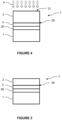
- the piezoelectric substrate 3 is then bonded to the support substrate 1 via the dielectric layer 4 and the adhesive layer 2, in order to form an assembled substrate 5, one embodiment of which is shown in FIG. figure 3 .
- the assembled substrate 5 is thus formed from the superposition of the support substrate 1, the adhesive layer 2, the dielectric layer 4, and the piezoelectric substrate 3, the adhesive layer 2 and the dielectric layer 4 being at the interface between the support substrate 1 and the piezoelectric substrate 3.
- the rough surface 30 of the piezoelectric layer 3 is thus at the interface of said piezoelectric layer 3 and the dielectric layer 4, and is adapted to reflect a radiofrequency wave which moves in the piezoelectric layer.
- the bonding is preferably carried out at room temperature, i.e. around 20°C. However, it is possible to carry out the hot bonding at a temperature between 20°C and 50°C, and more preferably between 20°C and 30°C.
- the bonding step is advantageously carried out at low pressure, i.e. at a pressure less than or equal to 5 mTorr, which makes it possible to desorb water from the surfaces forming the bonding interface, i.e. the surface of the adhesive layer and the rough surface of the piezoelectric substrate. Carrying out the bonding step under vacuum makes it possible to further improve the desorption of water at the bonding interface.
- the use of the polymer layer 2 as a bonding layer makes it possible on the one hand to bond the piezoelectric substrate 3 with the support substrate 1 effectively, in particular because the surface 30 of the piezoelectric substrate is rough, and it is commonly accepted that a polymer material bonds more easily to a slightly rough surface.
- the deposition of the adhesive layer 2, the assembly of the substrates 1 and 3, and the irradiation of the assembled substrate 5 are carried out more quickly and in a simplified manner compared to the techniques of the state of the art for which the successive depositions of SiO 2 layers on the rough surface and on the surface opposite the rough surface of the piezoelectric layer are long and tedious to implement.
- the proposed process presents a greatly reduced cost, since the deposition and UV irradiation of the adhesive layer are much less expensive than the successive SiO 2 depositions, and do not require the performance of chemical-mechanical polishing (CMP).
- CMP chemical-mechanical polishing
- the proposed polymer layer bonding also makes it possible to solve another major problem occurring during the successive depositions of SiO 2 layers, namely the creation of a significant unwanted curvature in the substrate, which hinders the manufacture of radiofrequency devices from said substrate, by avoiding such SiO 2 deposits.
- the method of the invention thus makes it possible to avoid, or at least reduce, the deformations of the piezoelectric substrate and the support substrate during the deposition of the dielectric layer and the adhesive layer respectively, as well as the final substrate obtained after bonding and irradiation.
- the assembled substrate 5 is then subjected to irradiation by a light flux 6, in order to polymerize the adhesive layer 2.
- the irradiation of the assembled substrate 5 is shown in the figure 4 .
- the light source is preferably a laser.
- the light radiation 5, or luminous flux is preferably ultraviolet (UV) radiation.
- UV radiation having a wavelength between 320 nm (nanometers) and 365 nm will preferably be chosen.
- the irradiation is carried out by exposing the free face 31 of the piezoelectric substrate to the incident light radiation 6.
- the light radiation penetrates into the assembled substrate 5 from the free face 31 of the piezoelectric substrate 3, passes through the piezoelectric substrate, passes through the dielectric layer 4, until reaching the adhesive layer 2, thus causing the polymerization of said adhesive layer.
- the polymerization of the adhesive layer makes it possible to form a polymer layer 20 which ensures the mechanical cohesion of the assembled substrate, by keeping the support substrate 1 and the piezoelectric substrate 3 bonded together, which form the final substrate 7.
- the irradiation of the assembled substrate 5 gives rise to a thermal process according to which the piezoelectric layer 3, crossed by the radiation, can partially absorb the energy of the radiation and heat up. Excessive heating would be likely to destabilize the structure of the piezoelectric layer, which could lead to a degradation of the physical and chemical properties of the piezoelectric layer. In addition, excessive heating would cause a deformation of the piezoelectric layer and the support substrate due to their difference in thermal expansion coefficient, leading to an overall deformation ("bow") of the assembled substrate and therefore of the resulting final substrate.
- bow overall deformation
- the irradiation is advantageously carried out in a pulsed manner, that is to say by exposing the assembled substrate to a plurality of pulses of light rays. Each pulse is carried out for a determined irradiation time, which may be equal or different from one pulse to another. The pulses are spaced in time by a determined rest time during which the assembled substrate is not exposed to the light rays.
- a person skilled in the art is able to determine the irradiation time of each pulse, the rest time between each pulse, as well as the number of pulses to be carried out to completely polymerize the adhesive layer.
- a final substrate consisting of the assembled substrate with a polymerized adhesive layer.
- the thickness of the polymerized adhesive layer 20 is preferably between 2 ⁇ m (micrometers) and 8 ⁇ m. This thickness depends in particular on the material constituting the photopolymerizable adhesive layer deposited before bonding, on the thickness of said photopolymerizable adhesive layer, and on the experimental irradiation conditions.
- the piezoelectric substrate 3 is thinned by removing material from the exposed face 31.
- This thinning step makes it possible to reduce the thickness of the piezoelectric layer and thus to obtain, on the support substrate 1, a piezoelectric layer 3 of a determined thickness.
- the final substrate 7 having a piezoelectric layer thinned 3 is shown on the figure 5
- the thinning step can in particular be carried out by etching and/or by mechanical-chemical polishing of the piezoelectric layer.
- a smoothing annealing of the thinned piezoelectric layer is preferably carried out. Smoothing consists of a surface treatment aimed at making the exposed surface of the piezoelectric layer flat and reducing its roughness.
- the steps of the method which are subsequent to the bonding of the piezoelectric substrate 3 on the support substrate 1 are carried out at a temperature less than or equal to 300°C, so as not to degrade their structure, in particular the structure of the adhesive layer 2, 20, nor to cause deformation of the substrates.
- a second subject of the invention relates to a method for manufacturing a radiofrequency device, such as a resonator or a filter, from a final substrate obtained by implementing the manufacturing method described above according to the first subject of the invention, as well as such a radiofrequency device.
- a radiofrequency device such as a resonator or a filter
- the described method is particularly suitable for the manufacture of a surface acoustic wave filter.
- it is first necessary to manufacture the final substrate according to the preceding method, then to form a pair of interdigitated electrodes on the surface of the piezoelectric layer of the final substrate.
- FIG. 6 is a principle view of a surface acoustic wave filter 10 according to one embodiment, manufactured from a final substrate 7 as previously described.
- the filter comprises a piezoelectric layer 3 and two electrodes 11, 12 in the form of two interdigitated metal combs deposited on the surface 31 of said piezoelectric layer.
- the piezoelectric layer 3 rests via its rough surface 30 on a dielectric layer 4, a polymerized adhesive layer 20, and a support substrate 1.
- the piezoelectric layer 3 is monocrystalline, an excellent crystalline quality being indeed necessary in order not to generate attenuation of the surface wave.
- the performance of such a surface acoustic wave filter is improved because the dielectric layer on the piezoelectric layer has a rough and contrasting interface in acoustic impedance.
- a polymerized adhesive layer in contact with the piezoelectric layer would have significant adverse influences on the performance.
Landscapes
- Physics & Mathematics (AREA)
- Acoustics & Sound (AREA)
- Engineering & Computer Science (AREA)
- Manufacturing & Machinery (AREA)
- Chemical & Material Sciences (AREA)
- Organic Chemistry (AREA)
- Surface Acoustic Wave Elements And Circuit Networks Thereof (AREA)
- Piezo-Electric Or Mechanical Vibrators, Or Delay Or Filter Circuits (AREA)
Applications Claiming Priority (2)
| Application Number | Priority Date | Filing Date | Title |
|---|---|---|---|
| FR1852574A FR3079345B1 (fr) | 2018-03-26 | 2018-03-26 | Procede de fabrication d'un substrat pour dispositif radiofrequence |
| PCT/FR2019/050685 WO2019186053A1 (fr) | 2018-03-26 | 2019-03-26 | Procede de fabrication d'un substrat pour dispositif radiofrequence |
Publications (2)
| Publication Number | Publication Date |
|---|---|
| EP3776632A1 EP3776632A1 (fr) | 2021-02-17 |
| EP3776632B1 true EP3776632B1 (fr) | 2024-08-21 |
Family
ID=62751059
Family Applications (1)
| Application Number | Title | Priority Date | Filing Date |
|---|---|---|---|
| EP19719549.8A Active EP3776632B1 (fr) | 2018-03-26 | 2019-03-26 | Procede de fabrication d'un substrat pour dispositif radiofrequence |
Country Status (8)
| Country | Link |
|---|---|
| US (2) | US11870411B2 (cg-RX-API-DMAC7.html) |
| EP (1) | EP3776632B1 (cg-RX-API-DMAC7.html) |
| JP (2) | JP2021519537A (cg-RX-API-DMAC7.html) |
| KR (1) | KR20200136427A (cg-RX-API-DMAC7.html) |
| CN (1) | CN111919285B (cg-RX-API-DMAC7.html) |
| FR (1) | FR3079345B1 (cg-RX-API-DMAC7.html) |
| SG (1) | SG11202009404SA (cg-RX-API-DMAC7.html) |
| WO (1) | WO2019186053A1 (cg-RX-API-DMAC7.html) |
Families Citing this family (9)
| Publication number | Priority date | Publication date | Assignee | Title |
|---|---|---|---|---|
| FR3079345B1 (fr) * | 2018-03-26 | 2020-02-21 | Soitec | Procede de fabrication d'un substrat pour dispositif radiofrequence |
| SG10201905013VA (en) | 2018-06-11 | 2020-01-30 | Skyworks Solutions Inc | Acoustic wave device with spinel layer |
| US12063027B2 (en) | 2018-11-21 | 2024-08-13 | Skyworks Solutions, Inc. | Acoustic wave device with ceramic substrate |
| US11621690B2 (en) | 2019-02-26 | 2023-04-04 | Skyworks Solutions, Inc. | Method of manufacturing acoustic wave device with multi-layer substrate including ceramic |
| FR3108789B1 (fr) * | 2020-03-24 | 2023-12-08 | Soitec Silicon On Insulator | Procédé de fabrication d’une structure piézoélectrique pour dispositif radiofréquence et pouvant servir pour le transfert d’une couche piézoélectrique, et procédé de transfert d’une telle couche piézoélectrique |
| FR3108788B1 (fr) * | 2020-03-24 | 2026-01-23 | Soitec Silicon On Insulator | Procédé de fabrication d’une structure piézoélectrique pour dispositif radiofréquence et pouvant servir pour le transfert d’une couche piézoélectrique, et procédé de transfert d’une telle couche piézoélectrique |
| FR3131436B1 (fr) * | 2021-12-23 | 2025-04-25 | Soitec Silicon On Insulator | Procede de fabrication d’un substrat donneur |
| FR3131979B1 (fr) * | 2022-01-17 | 2025-03-21 | Soitec Silicon On Insulator | Procédé de fabrication d’un substrat donneur pour le transfert d’une couche piézoélectrique et procédé de transfert d’une couche piézoélectrique sur un substrat support |
| FR3150687A1 (fr) * | 2023-06-30 | 2025-01-03 | Soitec | Procédé de fabrication d’un substrat donneur pour le transfert d’une couche piézoélectrique sur un substrat support |
Citations (1)
| Publication number | Priority date | Publication date | Assignee | Title |
|---|---|---|---|---|
| US20120086312A1 (en) * | 2010-10-06 | 2012-04-12 | Hiroki Kobayashi | Composite substrate manufacturing method and composite substrate |
Family Cites Families (39)
| Publication number | Priority date | Publication date | Assignee | Title |
|---|---|---|---|---|
| JPS5961863U (ja) | 1982-10-20 | 1984-04-23 | アロイ工器株式会社 | 加圧気液併用型噴霧ノズル |
| EP1037272A4 (en) * | 1997-06-19 | 2004-07-28 | Asahi Chemical Ind | SILICON ON ISOLATOR (SOI) SUBSTRATE AND SEMICONDUCTOR COMPONENT AND METHOD FOR THE PRODUCTION THEREOF |
| JP3144345B2 (ja) * | 1997-06-27 | 2001-03-12 | 日本電気株式会社 | 弾性表面波チップの実装方法 |
| JP2001053579A (ja) * | 1999-06-02 | 2001-02-23 | Matsushita Electric Ind Co Ltd | 弾性表面波素子と移動体通信機器 |
| JP4820520B2 (ja) * | 2000-02-22 | 2011-11-24 | エヌエックスピー ビー ヴィ | 担体基板上の音響反射層に音響共振子を備えた圧電フィルタの製造方法 |
| JP3520853B2 (ja) | 2001-01-26 | 2004-04-19 | 株式会社村田製作所 | 弾性表面波素子及びその製造方法 |
| KR100889886B1 (ko) | 2003-01-07 | 2009-03-20 | 에스. 오. 이. 떼끄 씰리꽁 오 냉쉴라또흐 떼끄놀로지 | 박층을 박리한 후 다층 구조를 포함하는 웨이퍼의 재활용방법 |
| US7031600B2 (en) * | 2003-04-07 | 2006-04-18 | Applied Materials, Inc. | Method and apparatus for silicon oxide deposition on large area substrates |
| JP2005011393A (ja) | 2003-06-17 | 2005-01-13 | Fuji Photo Film Co Ltd | 光情報媒体の製造方法 |
| JP2007501525A (ja) | 2003-08-04 | 2007-01-25 | ナノシス・インコーポレイテッド | ナノワイヤ複合体およびこれらに由来する電子基板を作製するためのシステムおよび方法 |
| JP2005229455A (ja) * | 2004-02-16 | 2005-08-25 | Shin Etsu Chem Co Ltd | 複合圧電基板 |
| JP2005231262A (ja) * | 2004-02-20 | 2005-09-02 | Keyence Corp | 紫外線照射装置、紫外線照射方法、紫外線照射条件設定プログラム及びコンピュータで読み取り可能な記録媒体並びに記憶した機器 |
| KR101368748B1 (ko) * | 2004-06-04 | 2014-03-05 | 더 보오드 오브 트러스티스 오브 더 유니버시티 오브 일리노이즈 | 인쇄가능한 반도체소자들의 제조 및 조립방법과 장치 |
| US8232182B2 (en) * | 2004-09-07 | 2012-07-31 | Massachusetts Institute Of Technology | Fabrication of electronic and photonic systems on flexible substrates by layer transfer method |
| FR2888663B1 (fr) * | 2005-07-13 | 2008-04-18 | Soitec Silicon On Insulator | Procede de diminution de la rugosite d'une couche epaisse d'isolant |
| JP2007221665A (ja) | 2006-02-20 | 2007-08-30 | Toshiba Corp | 薄膜圧電共振器及びその製造方法、並びに、これを用いたフィルタ |
| US7935568B2 (en) * | 2006-10-31 | 2011-05-03 | Tessera Technologies Ireland Limited | Wafer-level fabrication of lidded chips with electrodeposited dielectric coating |
| FR2933233B1 (fr) * | 2008-06-30 | 2010-11-26 | Soitec Silicon On Insulator | Substrat de haute resistivite bon marche et procede de fabrication associe |
| US8886334B2 (en) * | 2008-10-07 | 2014-11-11 | Mc10, Inc. | Systems, methods, and devices using stretchable or flexible electronics for medical applications |
| KR101706915B1 (ko) * | 2009-05-12 | 2017-02-15 | 더 보드 오브 트러스티즈 오브 더 유니버시티 오브 일리노이 | 변형가능 및 반투과 디스플레이를 위한 초박형, 미세구조 무기발광다이오드의 인쇄 어셈블리 |
| JP2011019043A (ja) * | 2009-07-08 | 2011-01-27 | Ngk Insulators Ltd | 複合基板及び複合基板の製造方法 |
| JP5429200B2 (ja) * | 2010-05-17 | 2014-02-26 | 株式会社村田製作所 | 複合圧電基板の製造方法および圧電デバイス |
| WO2012021197A2 (en) * | 2010-05-21 | 2012-02-16 | Arizona Board Of Regents, For And On Behalf Of Arizona State University | Method of manufacturing electronic devices on both sides of a carrier substrate and electronic devices thereof |
| CN203014754U (zh) * | 2010-06-15 | 2013-06-19 | 日本碍子株式会社 | 复合基板 |
| JP5796316B2 (ja) * | 2011-03-22 | 2015-10-21 | 株式会社村田製作所 | 圧電デバイスの製造方法 |
| FR2973158B1 (fr) * | 2011-03-22 | 2014-02-28 | Soitec Silicon On Insulator | Procédé de fabrication d'un substrat de type semi-conducteur sur isolant pour applications radiofréquences |
| CN103765768B (zh) * | 2011-08-26 | 2016-06-01 | 株式会社村田制作所 | 压电器件以及压电器件的制造方法 |
| WO2013031651A1 (ja) * | 2011-09-02 | 2013-03-07 | 株式会社村田製作所 | 弾性波装置及びその製造方法 |
| FR2985601B1 (fr) | 2012-01-06 | 2016-06-03 | Soitec Silicon On Insulator | Procede de fabrication d'un substrat et structure semiconducteur |
| JP5961863B2 (ja) | 2012-04-04 | 2016-08-02 | 株式会社ユニバーサルエンターテインメント | 遊技機 |
| US9859458B2 (en) | 2015-06-19 | 2018-01-02 | QMAT, Inc. | Bond and release layer transfer process |
| FR3045678B1 (fr) * | 2015-12-22 | 2017-12-22 | Soitec Silicon On Insulator | Procede de fabrication d'une couche piezoelectrique monocristalline et dispositif microelectronique, photonique ou optique comprenant une telle couche |
| WO2017139542A1 (en) * | 2016-02-11 | 2017-08-17 | Skyworks Solutions, Inc. | Device packaging using a recyclable carrier substrate |
| JP6825822B2 (ja) | 2016-05-11 | 2021-02-03 | 京セラ株式会社 | 容量素子、弾性波素子および弾性波モジュール |
| FR3053532B1 (fr) | 2016-06-30 | 2018-11-16 | Soitec | Structure hybride pour dispositif a ondes acoustiques de surface |
| JP6250856B1 (ja) | 2016-07-20 | 2017-12-20 | 信越化学工業株式会社 | 表面弾性波デバイス用複合基板及びその製造方法とこの複合基板を用いた表面弾性波デバイス |
| JP6621384B2 (ja) * | 2016-07-20 | 2019-12-18 | 信越化学工業株式会社 | 弾性表面波デバイス用複合基板の製造方法 |
| JP6998650B2 (ja) * | 2016-08-10 | 2022-01-18 | 株式会社日本製鋼所 | 接合基板、弾性表面波素子、弾性表面波デバイスおよび接合基板の製造方法 |
| FR3079345B1 (fr) * | 2018-03-26 | 2020-02-21 | Soitec | Procede de fabrication d'un substrat pour dispositif radiofrequence |
-
2018
- 2018-03-26 FR FR1852574A patent/FR3079345B1/fr active Active
-
2019
- 2019-03-26 SG SG11202009404SA patent/SG11202009404SA/en unknown
- 2019-03-26 CN CN201980022402.2A patent/CN111919285B/zh active Active
- 2019-03-26 KR KR1020207029654A patent/KR20200136427A/ko not_active Ceased
- 2019-03-26 US US17/041,367 patent/US11870411B2/en active Active
- 2019-03-26 EP EP19719549.8A patent/EP3776632B1/fr active Active
- 2019-03-26 JP JP2020551935A patent/JP2021519537A/ja not_active Ceased
- 2019-03-26 WO PCT/FR2019/050685 patent/WO2019186053A1/fr not_active Ceased
-
2024
- 2024-01-04 US US18/404,685 patent/US12278608B2/en active Active
- 2024-07-12 JP JP2024112740A patent/JP2024128100A/ja active Pending
Patent Citations (1)
| Publication number | Priority date | Publication date | Assignee | Title |
|---|---|---|---|---|
| US20120086312A1 (en) * | 2010-10-06 | 2012-04-12 | Hiroki Kobayashi | Composite substrate manufacturing method and composite substrate |
Also Published As
| Publication number | Publication date |
|---|---|
| US20210075389A1 (en) | 2021-03-11 |
| EP3776632A1 (fr) | 2021-02-17 |
| CN111919285A (zh) | 2020-11-10 |
| JP2024128100A (ja) | 2024-09-20 |
| KR20200136427A (ko) | 2020-12-07 |
| US11870411B2 (en) | 2024-01-09 |
| FR3079345B1 (fr) | 2020-02-21 |
| FR3079345A1 (fr) | 2019-09-27 |
| US12278608B2 (en) | 2025-04-15 |
| US20240146275A1 (en) | 2024-05-02 |
| JP2021519537A (ja) | 2021-08-10 |
| SG11202009404SA (en) | 2020-10-29 |
| CN111919285B (zh) | 2024-03-29 |
| WO2019186053A1 (fr) | 2019-10-03 |
Similar Documents
| Publication | Publication Date | Title |
|---|---|---|
| EP3776641B1 (fr) | Procede de transfert d'une couche piezoelectrique sur un substrat support | |
| WO2019186053A1 (fr) | Procede de fabrication d'un substrat pour dispositif radiofrequence | |
| EP4309216B1 (fr) | Procédé de transfert d'une couche d'une hétérostructure | |
| FR3053532A1 (fr) | Structure hybride pour dispositif a ondes acoustiques de surface | |
| EP0801419A1 (fr) | Procédé d'obtention d'un film mince de matériau semiconducteur comprenant notamment des composants électroniques | |
| FR2880184A1 (fr) | Procede de detourage d'une structure obtenue par assemblage de deux plaques | |
| WO2017207911A1 (fr) | Structure hybride pour dispositif a ondes acoustiques de surface | |
| EP1759411A1 (fr) | Procede de transfert de plaques | |
| FR3046874A1 (fr) | Procede de fabrication de structures semi-conductrices incluant une couche a haute resistivite, et structures semi-conductrices apparentees | |
| EP3776630B1 (fr) | Procédé de fabrication d'un substrat pour filtre radiofréquence | |
| EP4128380B1 (fr) | Procede de fabrication d'une structure piezoelectrique pour dispositif radiofrequence et servant pour le transfert d'une couche piezoelectrique, et procede de transfert d'une telle couche piezoelectrique | |
| EP4391374A1 (fr) | Procédé de réalisation d'un filtre à ondes acoustiques de volume | |
| EP4466729A1 (fr) | Procédé de fabrication d'un substrat donneur pour le transfert d'une couche piézoélectrique et procédé de transfert d'une couche piézoélectrique sur un substrat support | |
| FR3150687A1 (fr) | Procédé de fabrication d’un substrat donneur pour le transfert d’une couche piézoélectrique sur un substrat support | |
| FR3108788A1 (fr) | Procédé de fabrication d’une structure piézoélectrique pour dispositif radiofréquence et pouvant servir pour le transfert d’une couche piézoélectrique, et procédé de transfert d’une telle couche piézoélectrique | |
| FR3141592A1 (fr) | Substrat piézoélectrique sur isolant (POI) et procédé de fabrication d’un substrat piézoélectrique sur isolant (POI) | |
| WO2022175618A1 (fr) | Dispositif pyroelectrique comprenant un substrat a couche superficielle pyroelectrique et procede de realisation | |
| FR3133514A1 (fr) | Procédé de correction d’épaisseur d’une couche piézoélectrique |
Legal Events
| Date | Code | Title | Description |
|---|---|---|---|
| STAA | Information on the status of an ep patent application or granted ep patent |
Free format text: STATUS: UNKNOWN |
|
| STAA | Information on the status of an ep patent application or granted ep patent |
Free format text: STATUS: THE INTERNATIONAL PUBLICATION HAS BEEN MADE |
|
| PUAI | Public reference made under article 153(3) epc to a published international application that has entered the european phase |
Free format text: ORIGINAL CODE: 0009012 |
|
| STAA | Information on the status of an ep patent application or granted ep patent |
Free format text: STATUS: REQUEST FOR EXAMINATION WAS MADE |
|
| 17P | Request for examination filed |
Effective date: 20201023 |
|
| AK | Designated contracting states |
Kind code of ref document: A1 Designated state(s): AL AT BE BG CH CY CZ DE DK EE ES FI FR GB GR HR HU IE IS IT LI LT LU LV MC MK MT NL NO PL PT RO RS SE SI SK SM TR |
|
| AX | Request for extension of the european patent |
Extension state: BA ME |
|
| DAV | Request for validation of the european patent (deleted) | ||
| DAX | Request for extension of the european patent (deleted) | ||
| STAA | Information on the status of an ep patent application or granted ep patent |
Free format text: STATUS: EXAMINATION IS IN PROGRESS |
|
| 17Q | First examination report despatched |
Effective date: 20230120 |
|
| REG | Reference to a national code |
Ref country code: DE Ref legal event code: R079 Free format text: PREVIOUS MAIN CLASS: H01L0021200000 Ipc: H10N0030073000 Ref document number: 602019057359 Country of ref document: DE |
|
| RIC1 | Information provided on ipc code assigned before grant |
Ipc: H01L 21/20 20060101ALI20240228BHEP Ipc: H03H 9/02 20060101ALI20240228BHEP Ipc: H10N 30/073 20230101AFI20240228BHEP |
|
| GRAP | Despatch of communication of intention to grant a patent |
Free format text: ORIGINAL CODE: EPIDOSNIGR1 |
|
| STAA | Information on the status of an ep patent application or granted ep patent |
Free format text: STATUS: GRANT OF PATENT IS INTENDED |
|
| INTG | Intention to grant announced |
Effective date: 20240412 |
|
| GRAS | Grant fee paid |
Free format text: ORIGINAL CODE: EPIDOSNIGR3 |
|
| GRAA | (expected) grant |
Free format text: ORIGINAL CODE: 0009210 |
|
| STAA | Information on the status of an ep patent application or granted ep patent |
Free format text: STATUS: THE PATENT HAS BEEN GRANTED |
|
| AK | Designated contracting states |
Kind code of ref document: B1 Designated state(s): AL AT BE BG CH CY CZ DE DK EE ES FI FR GB GR HR HU IE IS IT LI LT LU LV MC MK MT NL NO PL PT RO RS SE SI SK SM TR |
|
| REG | Reference to a national code |
Ref country code: GB Ref legal event code: FG4D Free format text: NOT ENGLISH |
|
| REG | Reference to a national code |
Ref country code: CH Ref legal event code: EP |
|
| REG | Reference to a national code |
Ref country code: IE Ref legal event code: FG4D Free format text: LANGUAGE OF EP DOCUMENT: FRENCH |
|
| REG | Reference to a national code |
Ref country code: DE Ref legal event code: R096 Ref document number: 602019057359 Country of ref document: DE |
|
| REG | Reference to a national code |
Ref country code: LT Ref legal event code: MG9D |
|
| REG | Reference to a national code |
Ref country code: NL Ref legal event code: MP Effective date: 20240821 |
|
| PG25 | Lapsed in a contracting state [announced via postgrant information from national office to epo] |
Ref country code: NO Free format text: LAPSE BECAUSE OF FAILURE TO SUBMIT A TRANSLATION OF THE DESCRIPTION OR TO PAY THE FEE WITHIN THE PRESCRIBED TIME-LIMIT Effective date: 20241121 |
|
| REG | Reference to a national code |
Ref country code: AT Ref legal event code: MK05 Ref document number: 1716891 Country of ref document: AT Kind code of ref document: T Effective date: 20240821 |
|
| PG25 | Lapsed in a contracting state [announced via postgrant information from national office to epo] |
Ref country code: NL Free format text: LAPSE BECAUSE OF FAILURE TO SUBMIT A TRANSLATION OF THE DESCRIPTION OR TO PAY THE FEE WITHIN THE PRESCRIBED TIME-LIMIT Effective date: 20240821 Ref country code: FI Free format text: LAPSE BECAUSE OF FAILURE TO SUBMIT A TRANSLATION OF THE DESCRIPTION OR TO PAY THE FEE WITHIN THE PRESCRIBED TIME-LIMIT Effective date: 20240821 Ref country code: PL Free format text: LAPSE BECAUSE OF FAILURE TO SUBMIT A TRANSLATION OF THE DESCRIPTION OR TO PAY THE FEE WITHIN THE PRESCRIBED TIME-LIMIT Effective date: 20240821 Ref country code: GR Free format text: LAPSE BECAUSE OF FAILURE TO SUBMIT A TRANSLATION OF THE DESCRIPTION OR TO PAY THE FEE WITHIN THE PRESCRIBED TIME-LIMIT Effective date: 20241122 Ref country code: PT Free format text: LAPSE BECAUSE OF FAILURE TO SUBMIT A TRANSLATION OF THE DESCRIPTION OR TO PAY THE FEE WITHIN THE PRESCRIBED TIME-LIMIT Effective date: 20241223 |
|
| PG25 | Lapsed in a contracting state [announced via postgrant information from national office to epo] |
Ref country code: BG Free format text: LAPSE BECAUSE OF FAILURE TO SUBMIT A TRANSLATION OF THE DESCRIPTION OR TO PAY THE FEE WITHIN THE PRESCRIBED TIME-LIMIT Effective date: 20240821 |
|
| PG25 | Lapsed in a contracting state [announced via postgrant information from national office to epo] |
Ref country code: LV Free format text: LAPSE BECAUSE OF FAILURE TO SUBMIT A TRANSLATION OF THE DESCRIPTION OR TO PAY THE FEE WITHIN THE PRESCRIBED TIME-LIMIT Effective date: 20240821 |
|
| PG25 | Lapsed in a contracting state [announced via postgrant information from national office to epo] |
Ref country code: IS Free format text: LAPSE BECAUSE OF FAILURE TO SUBMIT A TRANSLATION OF THE DESCRIPTION OR TO PAY THE FEE WITHIN THE PRESCRIBED TIME-LIMIT Effective date: 20241221 Ref country code: AT Free format text: LAPSE BECAUSE OF FAILURE TO SUBMIT A TRANSLATION OF THE DESCRIPTION OR TO PAY THE FEE WITHIN THE PRESCRIBED TIME-LIMIT Effective date: 20240821 |
|
| PG25 | Lapsed in a contracting state [announced via postgrant information from national office to epo] |
Ref country code: HR Free format text: LAPSE BECAUSE OF FAILURE TO SUBMIT A TRANSLATION OF THE DESCRIPTION OR TO PAY THE FEE WITHIN THE PRESCRIBED TIME-LIMIT Effective date: 20240821 |
|
| PG25 | Lapsed in a contracting state [announced via postgrant information from national office to epo] |
Ref country code: RS Free format text: LAPSE BECAUSE OF FAILURE TO SUBMIT A TRANSLATION OF THE DESCRIPTION OR TO PAY THE FEE WITHIN THE PRESCRIBED TIME-LIMIT Effective date: 20241121 Ref country code: ES Free format text: LAPSE BECAUSE OF FAILURE TO SUBMIT A TRANSLATION OF THE DESCRIPTION OR TO PAY THE FEE WITHIN THE PRESCRIBED TIME-LIMIT Effective date: 20240821 |
|
| PG25 | Lapsed in a contracting state [announced via postgrant information from national office to epo] |
Ref country code: RS Free format text: LAPSE BECAUSE OF FAILURE TO SUBMIT A TRANSLATION OF THE DESCRIPTION OR TO PAY THE FEE WITHIN THE PRESCRIBED TIME-LIMIT Effective date: 20241121 Ref country code: PT Free format text: LAPSE BECAUSE OF FAILURE TO SUBMIT A TRANSLATION OF THE DESCRIPTION OR TO PAY THE FEE WITHIN THE PRESCRIBED TIME-LIMIT Effective date: 20241223 Ref country code: PL Free format text: LAPSE BECAUSE OF FAILURE TO SUBMIT A TRANSLATION OF THE DESCRIPTION OR TO PAY THE FEE WITHIN THE PRESCRIBED TIME-LIMIT Effective date: 20240821 Ref country code: NO Free format text: LAPSE BECAUSE OF FAILURE TO SUBMIT A TRANSLATION OF THE DESCRIPTION OR TO PAY THE FEE WITHIN THE PRESCRIBED TIME-LIMIT Effective date: 20241121 Ref country code: NL Free format text: LAPSE BECAUSE OF FAILURE TO SUBMIT A TRANSLATION OF THE DESCRIPTION OR TO PAY THE FEE WITHIN THE PRESCRIBED TIME-LIMIT Effective date: 20240821 Ref country code: LV Free format text: LAPSE BECAUSE OF FAILURE TO SUBMIT A TRANSLATION OF THE DESCRIPTION OR TO PAY THE FEE WITHIN THE PRESCRIBED TIME-LIMIT Effective date: 20240821 Ref country code: IS Free format text: LAPSE BECAUSE OF FAILURE TO SUBMIT A TRANSLATION OF THE DESCRIPTION OR TO PAY THE FEE WITHIN THE PRESCRIBED TIME-LIMIT Effective date: 20241221 Ref country code: HR Free format text: LAPSE BECAUSE OF FAILURE TO SUBMIT A TRANSLATION OF THE DESCRIPTION OR TO PAY THE FEE WITHIN THE PRESCRIBED TIME-LIMIT Effective date: 20240821 Ref country code: GR Free format text: LAPSE BECAUSE OF FAILURE TO SUBMIT A TRANSLATION OF THE DESCRIPTION OR TO PAY THE FEE WITHIN THE PRESCRIBED TIME-LIMIT Effective date: 20241122 Ref country code: FI Free format text: LAPSE BECAUSE OF FAILURE TO SUBMIT A TRANSLATION OF THE DESCRIPTION OR TO PAY THE FEE WITHIN THE PRESCRIBED TIME-LIMIT Effective date: 20240821 Ref country code: ES Free format text: LAPSE BECAUSE OF FAILURE TO SUBMIT A TRANSLATION OF THE DESCRIPTION OR TO PAY THE FEE WITHIN THE PRESCRIBED TIME-LIMIT Effective date: 20240821 Ref country code: BG Free format text: LAPSE BECAUSE OF FAILURE TO SUBMIT A TRANSLATION OF THE DESCRIPTION OR TO PAY THE FEE WITHIN THE PRESCRIBED TIME-LIMIT Effective date: 20240821 Ref country code: AT Free format text: LAPSE BECAUSE OF FAILURE TO SUBMIT A TRANSLATION OF THE DESCRIPTION OR TO PAY THE FEE WITHIN THE PRESCRIBED TIME-LIMIT Effective date: 20240821 |
|
| PG25 | Lapsed in a contracting state [announced via postgrant information from national office to epo] |
Ref country code: DK Free format text: LAPSE BECAUSE OF FAILURE TO SUBMIT A TRANSLATION OF THE DESCRIPTION OR TO PAY THE FEE WITHIN THE PRESCRIBED TIME-LIMIT Effective date: 20240821 Ref country code: RO Free format text: LAPSE BECAUSE OF FAILURE TO SUBMIT A TRANSLATION OF THE DESCRIPTION OR TO PAY THE FEE WITHIN THE PRESCRIBED TIME-LIMIT Effective date: 20240821 Ref country code: SM Free format text: LAPSE BECAUSE OF FAILURE TO SUBMIT A TRANSLATION OF THE DESCRIPTION OR TO PAY THE FEE WITHIN THE PRESCRIBED TIME-LIMIT Effective date: 20240821 |
|
| PG25 | Lapsed in a contracting state [announced via postgrant information from national office to epo] |
Ref country code: EE Free format text: LAPSE BECAUSE OF FAILURE TO SUBMIT A TRANSLATION OF THE DESCRIPTION OR TO PAY THE FEE WITHIN THE PRESCRIBED TIME-LIMIT Effective date: 20240821 |
|
| PG25 | Lapsed in a contracting state [announced via postgrant information from national office to epo] |
Ref country code: CZ Free format text: LAPSE BECAUSE OF FAILURE TO SUBMIT A TRANSLATION OF THE DESCRIPTION OR TO PAY THE FEE WITHIN THE PRESCRIBED TIME-LIMIT Effective date: 20240821 |
|
| PG25 | Lapsed in a contracting state [announced via postgrant information from national office to epo] |
Ref country code: SK Free format text: LAPSE BECAUSE OF FAILURE TO SUBMIT A TRANSLATION OF THE DESCRIPTION OR TO PAY THE FEE WITHIN THE PRESCRIBED TIME-LIMIT Effective date: 20240821 Ref country code: IT Free format text: LAPSE BECAUSE OF FAILURE TO SUBMIT A TRANSLATION OF THE DESCRIPTION OR TO PAY THE FEE WITHIN THE PRESCRIBED TIME-LIMIT Effective date: 20240821 |
|
| REG | Reference to a national code |
Ref country code: DE Ref legal event code: R097 Ref document number: 602019057359 Country of ref document: DE |
|
| PLBE | No opposition filed within time limit |
Free format text: ORIGINAL CODE: 0009261 |
|
| STAA | Information on the status of an ep patent application or granted ep patent |
Free format text: STATUS: NO OPPOSITION FILED WITHIN TIME LIMIT |
|
| 26N | No opposition filed |
Effective date: 20250522 |
|
| PG25 | Lapsed in a contracting state [announced via postgrant information from national office to epo] |
Ref country code: SE Free format text: LAPSE BECAUSE OF FAILURE TO SUBMIT A TRANSLATION OF THE DESCRIPTION OR TO PAY THE FEE WITHIN THE PRESCRIBED TIME-LIMIT Effective date: 20240821 |
|
| PG25 | Lapsed in a contracting state [announced via postgrant information from national office to epo] |
Ref country code: MC Free format text: LAPSE BECAUSE OF FAILURE TO SUBMIT A TRANSLATION OF THE DESCRIPTION OR TO PAY THE FEE WITHIN THE PRESCRIBED TIME-LIMIT Effective date: 20240821 |
|
| REG | Reference to a national code |
Ref country code: CH Ref legal event code: H13 Free format text: ST27 STATUS EVENT CODE: U-0-0-H10-H13 (AS PROVIDED BY THE NATIONAL OFFICE) Effective date: 20251023 |
|
| PG25 | Lapsed in a contracting state [announced via postgrant information from national office to epo] |
Ref country code: LU Free format text: LAPSE BECAUSE OF NON-PAYMENT OF DUE FEES Effective date: 20250326 |
|
| GBPC | Gb: european patent ceased through non-payment of renewal fee |
Effective date: 20250326 |
|
| REG | Reference to a national code |
Ref country code: BE Ref legal event code: MM Effective date: 20250331 |
|
| PG25 | Lapsed in a contracting state [announced via postgrant information from national office to epo] |
Ref country code: GB Free format text: LAPSE BECAUSE OF NON-PAYMENT OF DUE FEES Effective date: 20250326 |
|
| PG25 | Lapsed in a contracting state [announced via postgrant information from national office to epo] |
Ref country code: BE Free format text: LAPSE BECAUSE OF NON-PAYMENT OF DUE FEES Effective date: 20250331 |
|
| PG25 | Lapsed in a contracting state [announced via postgrant information from national office to epo] |
Ref country code: CH Free format text: LAPSE BECAUSE OF NON-PAYMENT OF DUE FEES Effective date: 20250331 |
|
| PG25 | Lapsed in a contracting state [announced via postgrant information from national office to epo] |
Ref country code: IE Free format text: LAPSE BECAUSE OF NON-PAYMENT OF DUE FEES Effective date: 20250326 |
|
| PGFP | Annual fee paid to national office [announced via postgrant information from national office to epo] |
Ref country code: DE Payment date: 20260204 Year of fee payment: 8 |
|
| PGFP | Annual fee paid to national office [announced via postgrant information from national office to epo] |
Ref country code: FR Payment date: 20260209 Year of fee payment: 8 |
|
| PG25 | Lapsed in a contracting state [announced via postgrant information from national office to epo] |
Ref country code: CY Free format text: LAPSE BECAUSE OF FAILURE TO SUBMIT A TRANSLATION OF THE DESCRIPTION OR TO PAY THE FEE WITHIN THE PRESCRIBED TIME-LIMIT Effective date: 20240821 |
|
| PG25 | Lapsed in a contracting state [announced via postgrant information from national office to epo] |
Ref country code: LT Free format text: LAPSE BECAUSE OF FAILURE TO SUBMIT A TRANSLATION OF THE DESCRIPTION OR TO PAY THE FEE WITHIN THE PRESCRIBED TIME-LIMIT Effective date: 20240821 |
|
| PG25 | Lapsed in a contracting state [announced via postgrant information from national office to epo] |
Ref country code: TR Free format text: LAPSE BECAUSE OF FAILURE TO SUBMIT A TRANSLATION OF THE DESCRIPTION OR TO PAY THE FEE WITHIN THE PRESCRIBED TIME-LIMIT Effective date: 20240821 |