EP3776641B1 - Procede de transfert d'une couche piezoelectrique sur un substrat support - Google Patents
Procede de transfert d'une couche piezoelectrique sur un substrat support Download PDFInfo
- Publication number
- EP3776641B1 EP3776641B1 EP19718438.5A EP19718438A EP3776641B1 EP 3776641 B1 EP3776641 B1 EP 3776641B1 EP 19718438 A EP19718438 A EP 19718438A EP 3776641 B1 EP3776641 B1 EP 3776641B1
- Authority
- EP
- European Patent Office
- Prior art keywords
- substrate
- layer
- piezoelectric
- handling
- adhesive layer
- Prior art date
- Legal status (The legal status is an assumption and is not a legal conclusion. Google has not performed a legal analysis and makes no representation as to the accuracy of the status listed.)
- Active
Links
- 239000000758 substrate Substances 0.000 title claims description 174
- 238000000034 method Methods 0.000 title claims description 23
- 239000010410 layer Substances 0.000 claims description 87
- 239000012790 adhesive layer Substances 0.000 claims description 32
- 238000004519 manufacturing process Methods 0.000 claims description 11
- 238000000151 deposition Methods 0.000 claims description 10
- 150000004767 nitrides Chemical class 0.000 claims description 9
- 230000008021 deposition Effects 0.000 claims description 8
- 229910052710 silicon Inorganic materials 0.000 claims description 8
- 239000010703 silicon Substances 0.000 claims description 8
- PMHQVHHXPFUNSP-UHFFFAOYSA-M copper(1+);methylsulfanylmethane;bromide Chemical compound Br[Cu].CSC PMHQVHHXPFUNSP-UHFFFAOYSA-M 0.000 claims description 4
- 230000015572 biosynthetic process Effects 0.000 claims description 3
- 230000004907 flux Effects 0.000 claims description 3
- 239000011521 glass Substances 0.000 claims description 3
- 238000000926 separation method Methods 0.000 claims description 3
- JBRZTFJDHDCESZ-UHFFFAOYSA-N AsGa Chemical compound [As]#[Ga] JBRZTFJDHDCESZ-UHFFFAOYSA-N 0.000 claims description 2
- 229910052594 sapphire Inorganic materials 0.000 claims description 2
- 239000010980 sapphire Substances 0.000 claims description 2
- 230000001678 irradiating effect Effects 0.000 claims 1
- 239000000463 material Substances 0.000 description 11
- 238000000137 annealing Methods 0.000 description 8
- 230000003313 weakening effect Effects 0.000 description 8
- XUIMIQQOPSSXEZ-UHFFFAOYSA-N Silicon Chemical compound [Si] XUIMIQQOPSSXEZ-UHFFFAOYSA-N 0.000 description 7
- 230000005855 radiation Effects 0.000 description 7
- 238000002513 implantation Methods 0.000 description 5
- 238000007596 consolidation process Methods 0.000 description 4
- 238000010438 heat treatment Methods 0.000 description 4
- 229910004298 SiO 2 Inorganic materials 0.000 description 3
- 238000006116 polymerization reaction Methods 0.000 description 3
- VYPSYNLAJGMNEJ-UHFFFAOYSA-N Silicium dioxide Chemical compound O=[Si]=O VYPSYNLAJGMNEJ-UHFFFAOYSA-N 0.000 description 2
- 230000015556 catabolic process Effects 0.000 description 2
- 238000006731 degradation reaction Methods 0.000 description 2
- -1 hydrogen ions Chemical class 0.000 description 2
- 238000009413 insulation Methods 0.000 description 2
- 230000002045 lasting effect Effects 0.000 description 2
- 229920000642 polymer Polymers 0.000 description 2
- 229910052814 silicon oxide Inorganic materials 0.000 description 2
- 238000011282 treatment Methods 0.000 description 2
- 229910020286 SiOxNy Inorganic materials 0.000 description 1
- 230000006978 adaptation Effects 0.000 description 1
- 239000000853 adhesive Substances 0.000 description 1
- 238000004026 adhesive bonding Methods 0.000 description 1
- 230000001070 adhesive effect Effects 0.000 description 1
- 238000005119 centrifugation Methods 0.000 description 1
- 239000011248 coating agent Substances 0.000 description 1
- 238000000576 coating method Methods 0.000 description 1
- 238000005520 cutting process Methods 0.000 description 1
- 238000000280 densification Methods 0.000 description 1
- 230000001419 dependent effect Effects 0.000 description 1
- 239000001307 helium Substances 0.000 description 1
- 229910052734 helium Inorganic materials 0.000 description 1
- 239000001257 hydrogen Substances 0.000 description 1
- 229910052739 hydrogen Inorganic materials 0.000 description 1
- 239000000203 mixture Substances 0.000 description 1
- 238000000678 plasma activation Methods 0.000 description 1
- 239000004065 semiconductor Substances 0.000 description 1
- 238000004528 spin coating Methods 0.000 description 1
- 239000000126 substance Substances 0.000 description 1
- 238000004381 surface treatment Methods 0.000 description 1
- XLYOFNOQVPJJNP-UHFFFAOYSA-N water Substances O XLYOFNOQVPJJNP-UHFFFAOYSA-N 0.000 description 1
Images

Classifications
-
- H—ELECTRICITY
- H10—SEMICONDUCTOR DEVICES; ELECTRIC SOLID-STATE DEVICES NOT OTHERWISE PROVIDED FOR
- H10N—ELECTRIC SOLID-STATE DEVICES NOT OTHERWISE PROVIDED FOR
- H10N30/00—Piezoelectric or electrostrictive devices
- H10N30/01—Manufacture or treatment
- H10N30/05—Manufacture of multilayered piezoelectric or electrostrictive devices, or parts thereof, e.g. by stacking piezoelectric bodies and electrodes
- H10N30/057—Manufacture of multilayered piezoelectric or electrostrictive devices, or parts thereof, e.g. by stacking piezoelectric bodies and electrodes by stacking bulk piezoelectric or electrostrictive bodies and electrodes
-
- H—ELECTRICITY
- H10—SEMICONDUCTOR DEVICES; ELECTRIC SOLID-STATE DEVICES NOT OTHERWISE PROVIDED FOR
- H10N—ELECTRIC SOLID-STATE DEVICES NOT OTHERWISE PROVIDED FOR
- H10N30/00—Piezoelectric or electrostrictive devices
- H10N30/01—Manufacture or treatment
- H10N30/07—Forming of piezoelectric or electrostrictive parts or bodies on an electrical element or another base
- H10N30/072—Forming of piezoelectric or electrostrictive parts or bodies on an electrical element or another base by laminating or bonding of piezoelectric or electrostrictive bodies
- H10N30/073—Forming of piezoelectric or electrostrictive parts or bodies on an electrical element or another base by laminating or bonding of piezoelectric or electrostrictive bodies by fusion of metals or by adhesives
-
- H—ELECTRICITY
- H01—ELECTRIC ELEMENTS
- H01L—SEMICONDUCTOR DEVICES NOT COVERED BY CLASS H10
- H01L21/00—Processes or apparatus adapted for the manufacture or treatment of semiconductor or solid state devices or of parts thereof
- H01L21/70—Manufacture or treatment of devices consisting of a plurality of solid state components formed in or on a common substrate or of parts thereof; Manufacture of integrated circuit devices or of parts thereof
- H01L21/71—Manufacture of specific parts of devices defined in group H01L21/70
- H01L21/76—Making of isolation regions between components
- H01L21/762—Dielectric regions, e.g. EPIC dielectric isolation, LOCOS; Trench refilling techniques, SOI technology, use of channel stoppers
- H01L21/7624—Dielectric regions, e.g. EPIC dielectric isolation, LOCOS; Trench refilling techniques, SOI technology, use of channel stoppers using semiconductor on insulator [SOI] technology
- H01L21/76251—Dielectric regions, e.g. EPIC dielectric isolation, LOCOS; Trench refilling techniques, SOI technology, use of channel stoppers using semiconductor on insulator [SOI] technology using bonding techniques
- H01L21/76254—Dielectric regions, e.g. EPIC dielectric isolation, LOCOS; Trench refilling techniques, SOI technology, use of channel stoppers using semiconductor on insulator [SOI] technology using bonding techniques with separation/delamination along an ion implanted layer, e.g. Smart-cut, Unibond
-
- H—ELECTRICITY
- H03—ELECTRONIC CIRCUITRY
- H03H—IMPEDANCE NETWORKS, e.g. RESONANT CIRCUITS; RESONATORS
- H03H3/00—Apparatus or processes specially adapted for the manufacture of impedance networks, resonating circuits, resonators
- H03H3/007—Apparatus or processes specially adapted for the manufacture of impedance networks, resonating circuits, resonators for the manufacture of electromechanical resonators or networks
- H03H3/02—Apparatus or processes specially adapted for the manufacture of impedance networks, resonating circuits, resonators for the manufacture of electromechanical resonators or networks for the manufacture of piezoelectric or electrostrictive resonators or networks
- H03H2003/025—Apparatus or processes specially adapted for the manufacture of impedance networks, resonating circuits, resonators for the manufacture of electromechanical resonators or networks for the manufacture of piezoelectric or electrostrictive resonators or networks the resonators or networks comprising an acoustic mirror
-
- H—ELECTRICITY
- H03—ELECTRONIC CIRCUITRY
- H03H—IMPEDANCE NETWORKS, e.g. RESONANT CIRCUITS; RESONATORS
- H03H3/00—Apparatus or processes specially adapted for the manufacture of impedance networks, resonating circuits, resonators
- H03H3/007—Apparatus or processes specially adapted for the manufacture of impedance networks, resonating circuits, resonators for the manufacture of electromechanical resonators or networks
- H03H3/02—Apparatus or processes specially adapted for the manufacture of impedance networks, resonating circuits, resonators for the manufacture of electromechanical resonators or networks for the manufacture of piezoelectric or electrostrictive resonators or networks
Definitions
- the present invention relates to a method for manufacturing a donor substrate for the transfer of a piezoelectric layer, as well as a method for transferring such a piezoelectric layer.
- the invention finds particular application in the manufacture of radio frequency devices, such as resonators or filters.
- a radio frequency (RF) device such as a resonator or filter
- a substrate comprising successively, from its base towards its surface, a support substrate, generally made of a semiconductor material such as silicon, a electrically insulating layer and a piezoelectric layer.
- RF radio frequency
- Bulk acoustic wave (BAW, acronym for the Anglo-Saxon term “Bulk Acoustic Wave”) devices typically comprise a thin piezoelectric layer (that is to say with a thickness generally substantially less than 1 ⁇ m) and two electrodes arranged on each main face of said thin layer.
- An electrical signal typically a variation in electrical voltage, applied to an electrode is converted into an elastic wave which propagates through the piezoelectric layer. The propagation of this elastic wave is favored if the frequency of the wave corresponds to the frequency band of the filter. This wave is again converted into an electrical signal when reaching the electrode located on the opposite side.
- the piezoelectric layer is typically obtained by transferring a thick substrate of a piezoelectric material (for example obtained by cutting an ingot) onto a support substrate.
- the support substrate is for example a silicon substrate.
- the transfer of the piezoelectric layer involves bonding the thick piezoelectric substrate to the support substrate, followed by a thinning of the thick piezoelectric substrate, so as to leave only a thin piezoelectric layer on the support substrate, of the desired thickness for manufacturing of the RF device.
- a layer of oxide for example a silicon oxide SiO 2
- a layer of oxide is generally deposited on each of the two substrates, and said substrates are bonded via said oxide layers.
- Said consolidation annealing is typically carried out at a temperature between 100°C and 300°C.
- the piezoelectric material and the material of the support substrate having very different thermal expansion coefficients, the implementation of such annealing causes significant deformation of the assembly.
- a pseudo-donor substrate that is to say a heterostructure in which the thick piezoelectric substrate is glued to a handle substrate.
- the thick piezoelectric substrate is held between the handling substrate and the support substrate.
- the donor pseudo-substrate could thus be produced by assembling the thick piezoelectric substrate and a silicon substrate, each covered with an oxide layer.
- the deposition of an oxide layer on the thick piezoelectric substrate causes a significant curvature (“bow” according to Anglo-Saxon terminology) of said piezoelectric substrate, hardly compatible with the subsequent stages of the process, which are suitable for flat substrates.
- the heterostructure cannot be subjected to consolidation annealing due to the differences in thermal expansion coefficients between the thick piezoelectric substrate and the handling substrate.
- the bonding energy of the oxide layers of the two substrates remains very low, so that the mechanical strength of the donor pseudo-substrate is insufficient. Therefore, breakage at the bonding interface may occur during the step of thinning the thick piezoelectric substrate.
- An aim of the invention is to remedy the aforementioned drawbacks and in particular to design a donor substrate for the transfer of a thin piezoelectric layer from a thick substrate onto a support substrate, which is less expensive to produce, which has better resistance. mechanical and/or which has a lower curvature than existing substrates.
- the invention proposes a method according to the definition of claim 1.
- a photo-polymerizable adhesive layer to assemble the heterostructure constituting the donor substrate makes it possible to give said substrate good mechanical strength while avoiding the process steps implemented at high temperature likely to cause a significant curvature of the substrate. Furthermore, the formation of such an adhesive layer is very simple to implement and is inexpensive.
- a first object of the invention relates to a method of manufacturing a donor substrate for the transfer of a piezoelectric layer onto a support substrate.
- the donor substrate is manufactured by bonding a piezoelectric substrate to a handling substrate.
- the handling substrate is made of a material whose thermal expansion coefficient is close to that of the material of the support substrate onto which the piezoelectric layer is intended to be transferred.
- close is meant a difference in thermal expansion coefficient between the material of the handling substrate and the material of the support substrate less than or equal to 5%, and preferably equal to or close to 0%.
- Suitable materials are, for example, silicon, sapphire, polycrystalline aluminum nitride (AIN), or gallium arsenide (GaAs).
- AIN polycrystalline aluminum nitride
- GaAs gallium arsenide
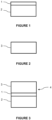
- a photo-polymerizable adhesive layer 1 is deposited on an exposed face of the handling substrate 2 or the piezoelectric substrate 3. On the figure 1 , the deposition is carried out on the handling substrate 2.
- the deposition of the photo-polymerizable adhesive layer 1 is advantageously carried out by centrifugal coating, or “spin coating” in English terminology.
- This technique consists of rotating the substrate on which the deposition of the photo-polymerizable layer is planned on itself at a substantially constant and relatively high speed, in order to spread said photo-polymerizable layer uniformly over the entire the surface of the substrate by centrifugal force.
- the substrate is typically placed and held by drawing vacuum on a rotating plate.
- the operating conditions such as the volume of adhesive deposited on the surface of the substrate, the rotation speed of the substrate, and the minimum duration of the deposition depending on the thickness desired for the adhesive layer.
- the thickness of the photo-polymerizable adhesive layer is typically between 2 and 8 ⁇ m.
- the photo-polymerizable adhesive layer sold under the reference “NOA 61” by the company NORLAND PRODUCTS can be used in the present invention.
- the piezoelectric substrate as shown in the figure 2 , is then glued to the handling substrate via the adhesive layer 1, in order to form a heterostructure 4, one embodiment of which is shown on the Figure 3 .
- the heterostructure 4 is thus formed from the superposition of the handling substrate 2, the adhesive layer 1, and the piezoelectric substrate 3, the adhesive layer being at the interface between the handling substrate and the piezoelectric substrate.
- Bonding is preferably carried out at room temperature, i.e. around 20°C. It is however possible to carry out hot bonding at a temperature between 20°C and 50°C, and more preferably between 20°C and 30°C.
- the bonding step is advantageously carried out under vacuum, which makes it possible to desorb the water from the surfaces forming the bonding interface, that is to say the surface of the adhesive layer and the surface of the substrate. manipulation or the piezoelectric substrate.
- the heterostructure 4 is then subjected to irradiation by a light flux 5, in order to polymerize the adhesive layer 1.
- the irradiation of the heterostructure is represented on the Figure 4 .
- the light source is preferably a laser.
- the light radiation, or luminous flux is preferably ultraviolet (UV) radiation.
- UV radiation having a wavelength of between 320 nm (nanometers) and 365 nm will preferably be chosen.
- Irradiation is carried out by exposing the free face 30 of the piezoelectric substrate 3 to incident light radiation.
- the light radiation 5 enters the heterostructure 4 from the free face 30 of the piezoelectric substrate, passes through the piezoelectric substrate 3, until reaching the adhesive layer 1, thus causing the polymerization of said adhesive layer.
- the polymerization of the adhesive layer 1 makes it possible to form a polymer layer 10 which ensures the mechanical cohesion of the heterostructure, by holding together the handling substrate 2 and the piezoelectric substrate 3 which form the donor substrate.
- the irradiation of the heterostructure gives rise to a thermal process according to which the piezoelectric layer, through which the radiation passes, can partly absorb the energy of the radiation and heat up. Too much heating would be likely to destabilize the structure of the piezoelectric layer, which could lead to a degradation of the physical and chemical properties of the piezoelectric layer. In addition, excessive heating would cause deformation of the piezoelectric layer and the handling substrate due to their difference in thermal expansion coefficient, resulting in an overall deformation, called "bow" in English terminology, of the heterostructure. and therefore the resulting donor substrate.
- the irradiation is advantageously carried out in an impulse manner, that is to say by exposing the heterostructure to a plurality of pulses of light rays. Each pulse is carried out for a determined irradiation time, which may be equal or different from one pulse to another. The pulses are spaced in time by a determined rest time during which the heterostructure is not exposed to light rays.
- a donor substrate 40 consisting of heterostructure 4 with a polymerized adhesive layer 10 is obtained.
- the polymerized adhesive layer makes it possible to bond the piezoelectric substrate and the handling substrate without exposing them to a thermal budget which would be likely to deform them, which makes it possible to give the donor substrate 40 sufficient mechanical strength for the subsequent transfer of a layer piezoelectric.
- the thickness of the polymerized adhesive layer 10 is preferably between 2 ⁇ m (micrometers) and 8 ⁇ m. This thickness depends in particular on the material constituting the photo-polymerizable adhesive layer deposited before bonding, on the thickness of said photo-polymerizable adhesive layer, and on the experimental irradiation conditions.
- the donor substrate 40 is subjected to a surface treatment aimed at making the exposed surface of the piezoelectric layer planar and reducing its roughness.
- a second object of the invention relates to a method of transferring a piezoelectric layer onto a support substrate.
- the donor substrate is preferably obtained by the manufacturing process described above according to the first object of the invention.
- the support substrate 6 is preferably made of silicon.
- a weakening zone 7 is formed in the piezoelectric substrate 3, so as to delimit the piezoelectric layer to be transferred 31.
- the depth of the weakening zone 7 relative to the exposed surface of the piezoelectric substrate determines the thickness of the piezoelectric layer to transfer.
- the weakening zone is formed by implantation of atomic species in the piezoelectric substrate, the implantation being represented on the Figure 5 by arrows 9.
- the atomic species are implanted at a determined depth of the piezoelectric substrate which determines the thickness of the piezoelectric layer to be transferred.
- the atomic species implanted are preferably hydrogen ions and/or helium ions.
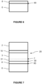
- a dielectric layer 8 is then formed on a main face of the support substrate 6 and/or the piezoelectric substrate.
- Figure 6 represents the support substrate 6 on which a dielectric layer 8 has been deposited.
- the dielectric layer is a layer of glass deposited by centrifugation on the piezoelectric substrate, called “spin-on glass” (SOG) according to Anglo-Saxon terminology.
- SOG spin-on glass
- This technique is advantageous in that the deposition of the layer is carried out at room temperature, and followed by densification annealing at a temperature of approximately 250°C, and therefore does not cause deformation of the substrate on which the layer dielectric is formed.
- the surface 30 or 60 to be bonded on which the dielectric layer has not been deposited, of the donor substrate 40 or of the support substrate 6, undergoes a suitable treatment to subsequently allow hydrophilic molecular bonding of this surface with the other respective surface.
- a suitable treatment consists of forming on the support substrate an oxide layer, or a nitride layer, or a layer comprising a combination of nitride and oxide, or a superposition of an oxide layer and 'a layer of nitride.
- an oxide layer SiO 2 or a nitride layer Si 3 N 4 , a layer comprising a combination of nitride and oxide SiOxNy, or a superposition of an oxide layer SiO 2 and a nitride layer Si 3 N 4 .
- a layer of silicon oxide will preferably be formed when the support substrate is made of silicon.
- the multilayer structure 20 formed then successively comprises the support substrate 6, the dielectric layer 8, the piezoelectric layer to be transferred 31 of the piezoelectric substrate 3, the polymer layer 10, and the manipulation substrate 2.
- the multilayer structure 20 is subjected to thermal annealing and the donor substrate 40 is detached from the support substrate 6 along the weakening zone 7, thus allowing the transfer of the piezoelectric layer 31 to the support substrate 6.
- FIG. 8 illustrates the final structure obtained after fracture and separation of the donor pseudo-substrate along the weakening zone, comprising the transferred piezoelectric layer 31 arranged on the support substrate 6, with the dielectric layer 8 located at the interface of the transferred piezoelectric layer 31 and the support substrate 6.
- the step of fracturing and separating the donor substrate is carried out at a temperature such that the polymerized adhesive layer is not degraded.
- a temperature less than or equal to 300°C makes it possible to avoid such degradation of the polymerized adhesive layer.
- a temperature of around 160°C is sufficient to fracture the piezoelectric substrate along the weakening zone.
- the piezoelectric substrate being held between two substrates (namely, the handling substrate and the support substrate) whose thermal expansion coefficients are close, it is not subject to differential deformation during the implementation of the annealing.
- a third object of the invention concerns a non-limiting application of the transfer method according to the second object of the invention.
- a method of manufacturing a volume acoustic wave device is proposed comprising the deposition of electrodes on two opposite faces of a piezoelectric layer manufactured according to the transfer method according to the second object of the invention.
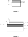
- FIG. 9 is a principle view of a bulk acoustic wave resonator.
- the resonator 70 comprises a thin piezoelectric layer 31 (that is to say with a thickness generally less than 1 ⁇ m, preferably less than 0.2 ⁇ m) and two electrodes 71, 72 arranged on either side of said piezoelectric layer 31.
- the piezoelectric layer 31 rests on a support substrate 6.
- a Bragg mirror 73 is interposed between the electrode 71 and the substrate 6. alternatively (not illustrated), this insulation could be achieved by providing a cavity between the substrate and the piezoelectric layer.
- the support substrate may not be optimal for the final application. It may then be advantageous to transfer layer 31 onto a final substrate (not shown) whose properties are chosen according to the intended application, by sticking it on said final substrate and removing the support substrate by any suitable technique.
- an adaptation of the method described above must be carried out.
- a first electrode on the free surface of the layer 31 to be transferred from the donor substrate this first electrode (referenced 71 on the Figure 9 ) being buried in the final pile.
- a second electrode referenced 72 on the Figure 9 .
- Another option is to transfer layer 31 onto a final substrate as mentioned above and to form the electrodes before and after said transfer.
- an insulation means can be integrated into it which can be, for example, a Bragg mirror (as illustrated in the Figure 9 ) or a cavity previously etched in the support substrate or in the final substrate if applicable.
Landscapes
- Engineering & Computer Science (AREA)
- Manufacturing & Machinery (AREA)
- Physics & Mathematics (AREA)
- Condensed Matter Physics & Semiconductors (AREA)
- General Physics & Mathematics (AREA)
- Computer Hardware Design (AREA)
- Microelectronics & Electronic Packaging (AREA)
- Power Engineering (AREA)
- Surface Acoustic Wave Elements And Circuit Networks Thereof (AREA)
- Piezo-Electric Or Mechanical Vibrators, Or Delay Or Filter Circuits (AREA)
- Piezo-Electric Transducers For Audible Bands (AREA)
Description
- La présente invention concerne un procédé de fabrication d'un substrat donneur pour le transfert d'une couché piézoélectrique, ainsi qu'un procédé de transfert d'une telle couche piézoélectrique. L'invention trouve notamment application dans la fabrication de dispositifs radiofréquence, tels que des résonateurs ou des filtres.
- Il est connu de fabriquer un dispositif radiofréquence (RF), tel qu'un résonateur ou filtre, sur un substrat comprenant successivement, de sa base vers sa surface, un substrat support, généralement en un matériau semi-conducteur tel que du silicium, une couche électriquement isolante et une couche piézoélectrique.
- Les dispositifs à ondes acoustiques de volume (BAW, acronyme du terme anglo-saxon « Bulk Acoustic Wave ») comprennent typiquement une couche piézoélectrique mince (c'est-à-dire d'épaisseur généralement sensiblement inférieure à 1 µm) et deux électrodes agencées sur chaque face principale de ladite couche mince. Un signal électrique, typiquement une variation de tension électrique, appliqué à une électrode est converti en onde élastique qui se propage au travers de la couche piézoélectrique. La propagation de cette onde élastique est favorisée si la fréquence de l'onde correspond à la bande de fréquence du filtre. Cette onde est à nouveau convertie en signal électrique en parvenant à l'électrode située sur la face opposée.
- La couche piézoélectrique est typiquement obtenue par transfert d'un substrat épais d'un matériau piézoélectrique (par exemple obtenu par découpe d'un lingot) sur un substrat support. Le substrat support est par exemple un substrat de silicium.
- Le transfert de la couche piézoélectrique implique un collage du substrat piézoélectrique épais sur le substrat support, suivi d'un amincissement du substrat piézoélectrique épais, de sorte à ne laisser sur le substrat support qu'une couche piézoélectrique mince, de l'épaisseur souhaitée pour la fabrication du dispositif RF.
- Pour une bonne adhésion du substrat piézoélectrique sur le substrat support, on procède généralement à un dépôt d'une couche d'oxyde (par exemple un oxyde de silicium SiO2) sur chacun des deux substrats, et on colle lesdits substrats par l'intermédiaire desdites couches d'oxyde.
- Pour renforcer un tel collage oxyde-oxyde, il est connu d'effectuer, avant le collage, une activation par plasma des surfaces à coller, et, après le collage, un recuit de consolidation.
- Ledit recuit de consolidation est typiquement réalisé à une température comprise entre 100°C et 300°C.
- Or, le matériau piézoélectrique et le matériau du substrat support présentant des coefficients de dilatation thermique très différents, la mise en oeuvre d'un tel recuit engendre une déformation importante de l'assemblage.
- Pour pallier ce type de problème, il est connu de recourir à un pseudo-substrat donneur, c'est-à-dire une hétérostructure dans laquelle le substrat piézoélectrique épais est collé sur un substrat de manipulation (« handle substrate » en anglais). Ainsi, après collage dudit pseudo-substrat donneur et du substrat support, le substrat piézoélectrique épais est maintenu entre le substrat de manipulation et le substrat support. Le choix des matériaux et des épaisseurs du substrat de manipulation et du substrat support permet d'assurer une certaine symétrie des coefficients de dilatation thermique, et ainsi de minimiser la déformation de l'assemblage lors l'application de traitements thermiques.
- Le pseudo-substrat donneur pourrait ainsi être réalisé par assemblage du substrat piézoélectrique épais et d'un substrat de silicium, chacun recouvert d'une couche d'oxyde.
- Cependant, une telle hétérostructure présente plusieurs inconvénients.
- D'une part, le dépôt d'une couche d'oxyde sur le substrat piézoélectrique épais provoque une courbure (« bow » selon la terminologie-anglo-saxonne) importante dudit substrat piézoélectrique, peu compatible avec les étapes ultérieures du procédé, qui sont adaptées à des substrats plans.
- Par ailleurs, la formation des couches d'oxyde nécessaires au collage est longue et coûteuse.
- Enfin, comme mentionné plus haut, l'hétérostructure ne peut être soumise au recuit de consolidation en raison des différences de coefficients de dilatation thermique entre le substrat piézoélectrique épais et le substrat de manipulation. Or, en l'absence du recuit de consolidation, l'énergie de collage des couches d'oxyde des deux substrats reste très faible, de sorte que la tenue mécanique du pseudo-substrat donneur est insuffisante. Par conséquent, une rupture au niveau de l'interface de collage peut se produire lors de l'étape d'amincissement du substrat piézoélectrique épais.
- Des procédés de transfert d'une couche mince à partir d'un substrat donneur vers un substrat receveur sont par exemple décrits dans
WO 2017/052646 ,EP 0924769 etUS 2003/0082889 . Dans ces documents, il n'y a aucune divulgation d'une étape de photopolymérisation en combinaison avec une étape de fracture d'une couche piézoélectrique le long d'une zone de fragilisation à l'intérieur de la couche piézoélectrique. - Un but de l'invention est de remédier aux inconvénients précités et notamment de concevoir un substrat donneur pour le transfert d'une couche piézoélectrique mince d'un substrat épais sur un substrat support, qui soit moins coûteux à réaliser, qui présente une meilleure tenue mécanique et/ou qui présente une courbure plus faible que les substrats existants.
- A cet effet, l'invention propose un procédé selon la définition de la revendication 1.
- La mise en oeuvre d'une couche adhésive photo-polymérisable pour assembler l'hétérostructure constituant le substrat donneur permet de conférer audit substrat une bonne tenue mécanique tout en s'affranchissant des étapes de procédé mises en oeuvre à haute température susceptibles d'engendrer une courbure importante du substrat. Par ailleurs, la formation d'une telle couche adhésive est très simple à mettre en oeuvre et est peu coûteuse.
- D'autres aspects sont définis par les revendications dépendantes.
- D'autres caractéristiques et avantages de l'invention ressortiront de la description détaillée qui va suivre, en référence aux dessins annexés sur lesquels :
- la
figure 1 illustre schématiquement l'étape de dépôt de la couche adhésive photo-polymérisable sur le substrat de manipulation ; - la
figure 2 illustre schématiquement l'étape de fourniture du substrat piézoélectrique épais ; - la
figure 3 illustre schématiquement une hétérostructure obtenue par collage du substrat piézoélectrique sur le substrat de manipulation par l'intermédiaire de la couche adhésive ; - la
figure 4 illustre schématiquement l'étape de polymérisation de la couche adhésive dans l'hétérostructure de sorte à former le pseudo-substrat donneur, dit simplement substrat donneur, selon l'invention ; - la
figure 5 illustre schématiquement l'étape d'implantation d'espèces atomiques dans le substrat donneur de lafigure 4 de manière à y former une zone de fragilisation ; - la
figure 6 illustre schématiquement un substrat support sur lequel a été déposée une couche diélectrique ; - la
figure 7 illustre schématiquement l'étape de collage du substrat donneur fragilisé sur le substrat support ; - la
figure 8 illustre le substrat obtenu après fracture et séparation du substrat donneur le long de la zone de fragilisation ; - la
figure 9 est une illustration schématique d'un filtre à onde acoustique de volume selon un mode de réalisation de l'invention. - Pour des raisons de lisibilité des figures, les éléments illustrés ne sont pas nécessairement représentés à l'échelle. Par ailleurs, les éléments désignés par les mêmes signes de référence sur différentes figures sont identiques ou remplissent la même fonction.
- Un premier objet de l'invention concerne un procédé de fabrication d'un substrat donneur pour le transfert d'une couche piézoélectrique sur un substrat support.
- Le substrat donneur est fabriqué par collage d'un substrat piézoélectrique sur un substrat de manipulation.
- Le substrat de manipulation est fabriqué dans un matériau dont le coefficient de dilatation thermique est proche de celui du matériau du substrat support sur lequel la couche piézoélectrique est destinée à être transférée. Par « proche », on entend une différence de coefficient de dilatation thermique entre le matériau du substrat de manipulation et le matériau du substrat support inférieure ou égale à 5%, et de préférence égale ou voisine de 0%. Des matériaux adaptés sont par exemple le silicium, le saphir, le nitrure d'aluminium (AIN) polycristallin, ou encore l'arséniure de gallium (GaAs). Dans la présente invention, on s'intéresse au coefficient de dilatation thermique dans un plan parallèle à la surface principale des substrats.
- Selon une première étape représentée sur la
figure 1 , une couche adhésive photo-polymérisable 1 est déposée sur une face exposée du substrat de manipulation 2 ou du substrat piézoélectrique 3. Sur lafigure 1 , le dépôt est effectué sur le substrat de manipulation 2. - Le dépôt de la couche adhésive photo-polymérisable 1 est avantageusement effectué par enduction centrifuge, ou « spin coating » en terminologie anglosaxonne. Cette technique consiste à faire tourner le substrat sur lequel est prévu le dépôt de la couche photo-polymérisable sur lui-même à une vitesse sensiblement constante et relativement élevée, afin d'étaler ladite couche photo-polymérisable de façon uniforme sur l'ensemble de la surface du substrat par force centrifuge. A cet effet, le substrat est typiquement posé et maintenu par tirage du vide sur un plateau tournant.
- L'homme du métier est en mesure de déterminer les conditions opératoires, telles que le volume d'adhésif déposé sur la surface du substrat, la vitesse de rotation du substrat, et la durée minimale du dépôt en fonction de l'épaisseur souhaitée pour la couche adhésive.
- L'épaisseur de la couche adhésive photo-polymérisable est typiquement comprise entre 2 et 8 µm.
- Selon un exemple non limitatif, la couche adhésive photo-polymérisable commercialisée sous la référence « NOA 61 » par la société NORLAND PRODUCTS peut être utilisée dans la présente invention.
- Le substrat piézoélectrique, tel que représenté sur la
figure 2 , est ensuite collé sur le substrat de manipulation par l'intermédiaire de la couche adhésive 1, afin de former une hétérostructure 4, dont un mode de réalisation est représenté sur lafigure 3 . - L'hétérostructure 4 est ainsi formée de la superposition du substrat de manipulation 2, de la couche adhésive 1, et du substrat piézoélectrique 3, la couche adhésive se trouvant à l'interface entre le substrat de manipulation et le substrat piézoélectrique.
- Le collage est de préférence réalisé à température ambiante, soit environ 20°C. Il est cependant possible de réaliser le collage à chaud à une température comprise entre 20°C et 50°C, et de manière davantage préférée entre 20°C et 30°C.
- De plus, l'étape de collage est avantageusement effectuée sous vide, ce qui permet de désorber l'eau des surfaces formant l'interface de collage, c'est-à-dire la surface de la couche adhésive et la surface du substrat de manipulation ou du substrat piézoélectrique.
- On soumet ensuite l'hétérostructure 4 à une irradiation par un flux lumineux 5, afin de polymériser la couche adhésive 1. L'irradiation de l'hétérostructure et représentée sur la
figure 4 . - La source lumineuse est de préférence un laser.
- Le rayonnement lumineux, ou flux lumineux, est de préférence un rayonnement ultra-violet (UV). En fonction de la composition de la couche adhésive, on choisira de préférence un rayonnement UV présentant une longueur d'onde comprise entre 320 nm (nanomètres) et 365 nm.
- L'irradiation est effectuée en exposant la face libre 30 du substrat piézoélectrique 3 au rayonnement lumineux incident. Ainsi, le rayonnement lumineux 5 pénètre dans l'hétérostructure 4 depuis la face libre 30 du substrat piézoélectrique, traverse le substrat piézoélectrique 3, jusqu'à atteindre la couche adhésive 1, provoquant ainsi la polymérisation de ladite couche adhésive.
- La polymérisation de la couche adhésive 1 permet de former une couche polymère 10 qui assure la cohésion mécanique de l'hétérostructure, en maintenant collés ensemble le substrat de manipulation 2 et le substrat piézoélectrique 3 qui forment le substrat donneur.
- L'irradiation de l'hétérostructure donne lieu à un processus thermique selon lequel la couche piézoélectrique, traversée par le rayonnement, peut absorber en partie l'énergie du rayonnement et s'échauffer. Un échauffement trop important serait susceptible de déstabiliser la structure de la couche piézoélectrique, ce qui pourrait aboutir à une dégradation des propriétés physiques et chimiques de la couche piézoélectrique. En outre, un échauffement trop important occasionnerait une déformation de la couche piézoélectrique et du substrat de manipulation en raison de leur différence de coefficient de dilatation thermique, aboutissant à une déformation globale, dite « bow » en terminologie anglo-saxonne, de l'hétérostructure et donc du substrat donneur résultant.
- Afin d'éviter un échauffement trop important de la couche piézoélectrique, l'irradiation est avantageusement effectuée de manière impulsionnelle, c'est-à-dire en exposant l'hétérostructure à une pluralité d'impulsions de rayons lumineux. Chaque impulsion est réalisée pendant un temps d'irradiation déterminé, qui peut être égal ou différent d'une impulsion à l'autre. Les impulsions sont espacées dans le temps par un temps de repos déterminé pendant lequel l'hétérostructure n'est pas exposée aux rayons lumineux.
- L'homme du métier est en mesure de déterminer le temps d'irradiation de chaque impulsion, le temps de repos entre chaque impulsion, ainsi que le nombre d'impulsions à réaliser pour polymériser complètement la couche adhésive.
- Ainsi, par exemple, on pourra mettre en oeuvre une dizaine d'impulsions durant 10 secondes chacune, séparées par des temps de repos durant également 10 secondes chacun.
- Après irradiation, on obtient un substrat donneur 40 constitué de l'hétérostructure 4 avec une couche adhésive polymérisée 10.
- La couche adhésive polymérisée permet de coller le substrat piézoélectrique et le substrat de manipulation sans les exposer à un budget thermique qui serait susceptible de les déformer, ce qui permet de conférer au substrat donneur 40 une tenue mécanique suffisante pour le transfert ultérieur d'une couche piézoélectrique.
- L'épaisseur de la couche adhésive polymérisée 10 est de préférence comprise entre 2 µm (micromètres) et 8 µm. Cette épaisseur dépend notamment du matériau constitutif de la couche adhésive photo-polymérisable déposée avant collage, de l'épaisseur de ladite couche adhésive photo-polymérisable, et des conditions expérimentales d'irradiation.
- De manière optionnelle, le substrat donneur 40 est soumis à un traitement de surface visant à rendre la surface exposée de la couche piézoélectrique plane et à en réduire la rugosité.
- Un deuxième objet de l'invention concerne un procédé de transfert d'une couche piézoélectrique sur un substrat support.
- On fournit initialement un substrat donneur comprenant la couche piézoélectrique à transférer. Le substrat donneur est de préférence obtenu par le procédé de fabrication décrit précédemment selon le premier objet de l'invention.
- On fournit également un substrat support 6 apte à recevoir la couche piézoélectrique à transférer. Le substrat support est de préférence en silicium.
- Selon une première étape représentée sur la
figure 5 , on forme une zone de fragilisation 7 dans le substrat piézoélectrique 3, de manière à délimiter la couche piézoélectrique à transférer 31. La profondeur de la zone de fragilisation 7 par rapport à la surface exposée du substrat piézoélectrique détermine l'épaisseur de la couche piézoélectrique à transférer. - Selon un mode de réalisation préféré, la zone de fragilisation est formée par implantation d'espèces atomiques dans le substrat piézoélectrique, l'implantation étant représentée sur la
figure 5 par les flèches 9. Les espèces atomiques sont implantées à une profondeur déterminée du substrat piézoélectrique qui détermine l'épaisseur de la couche piézoélectrique à transférer. - Lorsque la zone de fragilisation est formée par implantation d'espèces atomiques, les espèces atomiques implantées sont de préférence des ions hydrogène et/ou des ions hélium.
- On forme ensuite une couche diélectrique 8 sur une face principale du substrat support 6 et/ou du substrat piézoélectrique. La
figure 6 représente le substrat support 6 sur lequel a été déposée une couche diélectrique 8. - De préférence, la couche diélectrique est une couche de verre déposée par centrifugation sur le substrat piézoélectrique, dite « spin-on glass » (SOG) selon la terminologie anglo-saxonne. Cette technique est avantageuse en ce que le dépôt de la couche est effectuée à température ambiante, et suivie d'un recuit de densification à une température d'environ 250°C, et n'engendre donc pas de déformation du substrat sur lequel la couche diélectrique est formée.
- De manière optionnelle, la surface 30 ou 60 à coller sur laquelle la couche diélectrique n'a pas été déposée, du substrat donneur 40 ou du substrat support 6, subit un traitement adapté pour permettre ultérieurement un collage moléculaire hydrophile de cette surface avec l'autre surface respective. De préférence, un tel traitement consiste à former sur le substrat support une couche d'oxyde, ou une couche de nitrure, ou une couche comprenant une combinaison de nitrure et d'oxyde, ou une superposition d'une couche d'oxyde et d'une couche de nitrure. Par exemple, dans le cas d'un substrat support en silicium, on pourra former une couche d'oxyde SiO2, ou une couche de nitrure Si3N4, une couche comprenant une combinaison de nitrure et d'oxyde SiOxNy, ou une superposition d'une couche d'oxyde SiO2 et d'une couche de nitrure Si3N4.
- On formera de préférence une couche d'oxyde de silicium lorsque le substrat support est en silicium.
- On procède par la suite au collage du substrat donneur 40 sur le substrat support 6, tel qu'illustré sur la
figure 7 . - Le collage est effectué de manière à ce que la couche diélectrique 8 se trouve à l'interface de collage. La structure multicouche 20 formée comprend alors successivement le substrat support 6, la couche diélectrique 8, la couche piézoélectrique à transférer 31 du substrat piézoélectrique 3, la couche polymère 10, et le substrat de manipulation 2.
- Après collage, la structure multicouche 20 est soumise à un recuit thermique et la substrat donneur 40 est détaché du substrat support 6 le long de la zone de fragilisation 7, permettant ainsi le transfert de la couche piézoélectrique 31 sur le substrat support 6.
- La
figure 8 illustre la structure finale obtenue après fracture et séparation du pseudo-substrat donneur le long de la zone de fragilisation, comprenant la couche piézoélectrique transférée 31 agencée sur le substrat support 6, avec la couche diélectrique 8 située à l'interface de la couche piézoélectrique transférée 31 et du substrat support 6. - L'étape de fracture et de séparation du substrat donneur est effectuée à une température telle que la couche adhésive polymérisée n'est pas dégradée. Une température inférieure ou égale à 300°C permet d'éviter une telle dégradation de la couche adhésive polymérisée. Une température de l'ordre de 160°C est suffisante pour fracturer le substrat piézoélectrique le long de la zone de fragilisation.
- Le substrat piézoélectrique étant maintenu entre deux substrats (à savoir, le substrat de manipulation et le substrat support) dont les coefficients de dilatation thermique sont proches, il n'est pas soumis à une déformation différentielle lors de la mise en oeuvre du recuit.
- Un troisième objet de l'invention concerne une application non limitative du procédé de transfert selon le deuxième objet de l'invention. Il est proposé un procédé de fabrication d'un dispositif à ondes acoustiques de volume comprenant le dépôt d'électrodes sur deux faces opposées d'une couche piézoélectrique fabriquée selon le procédé de transfert selon le deuxième objet de l'invention.
- La
figure 9 est une vue de principe d'un résonateur à ondes acoustiques de volume. - Le résonateur 70 comprend une couche piézoélectrique mince 31 (c'est-à-dire d'épaisseur généralement inférieure à 1 µm, de préférence inférieure à 0,2 µm) et deux électrodes 71, 72 agencées de part et d'autre de ladite couche piézoélectrique 31. La couche piézoélectrique 31 repose sur un substrat support 6. Pour isoler le résonateur du substrat et éviter ainsi la propagation des ondes dans le substrat, un miroir de Bragg 73 est interposé entre l'électrode 71 et le substrat 6. De manière alternative (non illustrée), cette isolation pourrait être réalisée en ménageant une cavité entre le substrat et la couche piézoélectrique. Ces différentes dispositions sont connues de l'homme du métier et ne seront donc pas décrites en détail dans le présent texte.
- Dans certains cas, le substrat support peut ne pas être optimal pour l'application finale. Il peut alors être avantageux de transférer la couche 31 sur un substrat final (non représenté) dont les propriétés sont choisies en fonction de l'application visée, en la collant sur ledit substrat final et en retirant le substrat support par toute technique adaptée.
- Pour fabriquer un dispositif à ondes acoustiques de volume, selon un mode de réalisation, une adaptation du procédé décrit précédemment doit être effectuée. D'une part, on dépose, avant l'étape de collage illustrée sur la
figure 7 , une première électrode sur la surface libre de la couche 31 à transférer du substrat donneur, cette première électrode (référencée 71 sur lafigure 9 ) se trouvant enterrée dans l'empilement final. Après l'étape de transfert illustrée sur lafigure 8 , on dépose une seconde électrode (référencée 72 sur lafigure 9 ) sur la surface libre de la couche 31, opposée à la première électrode. Une autre option est de transférer la couche 31 sur un substrat final comme mentionné plus haut et de former les électrodes avant et après ledit transfert. D'autre part, pour éviter la propagation des ondes acoustiques dans le substrat support 6, on peut intégrer à celui-ci un moyen d'isolation pouvant être, par exemple, un miroir de Bragg (comme illustré sur lafigure 9 ) ou une cavité préalablement gravée dans le substrat support ou dans le substrat final le cas échéant. - Enfin, il va de soi que l'application que l'on vient de donner n'est qu'une illustration particulière en aucun cas limitative quant aux domaines d'application de l'invention.
Claims (8)
- Procédé de transfert d'une couche piézoélectrique (3) sur un substrat support (6), comprenant :- la fourniture d'un substrat donneur (40) constitué d'une hétérostructure (4) comprenant un substrat piézoélectrique (3) collé sur un substrat de manipulation (2), et une couche adhésive polymérisée par photopolymérisation (10) à l'interface entre le substrat piézoélectrique (3) et le substrat de manipulation (2),- la formation d'une zone de fragilisation (7) dans le substrat piézoélectrique (3), de manière à délimiter la couche piézoélectrique à transférer (31),- la fourniture du substrat support (6),- la formation d'une couche diélectrique (8) sur une face principale du substrat support (6) et/ou du substrat piézoélectrique (3),- le collage du substrat donneur (40) sur le substrat support (6), ladite couche diélectrique (8) étant à l'interface de collage,- la fracture et la séparation du substrat donneur (40) le long de la zone de fragilisation (7), à une température inférieure ou égale à 300°C.
- Procédé selon la revendication 1, dans lequel la couche diélectrique (8) est une couche de verre déposée par centrifugation sur le substrat piézoélectrique.
- Procédé selon la revendication 1 ou la revendication 2, comprenant, avant le collage, la formation d'une couche d'oxyde, ou une couche de nitrure, ou une couche comprenant une combinaison de nitrure et d'oxyde, ou une superposition d'au moins une couche d'oxyde et d'une couche de nitrure sur le substrat support (6).
- Procédé selon l'une quelconque des revendications 1 à 3, dans lequel la formation de la zone de fragilisation (7) est effectuée par implantation d'espèces atomiques (9) dans le substrat piézoélectrique.
- Procédé selon l'une quelconque des revendications 1 à 4, dans lequel le substrat de manipulation (2) est un substrat en silicium, en saphir, en nitrure d'aluminium (AIN) polycristallin, ou en arséniure de gallium (GaAs).
- Procédé selon l'une quelconque des revendications 1 à 5, dans lequel l'épaisseur de la couche adhésive polymérisée (10) est comprise entre 2 µm et 8 µm.
- Procédé selon l'une des revendications 1 à 6, comprenant la fabrication du substrat donneur (40) par les étapes suivantes :- la fourniture du substrat piézoélectrique (3),- la fourniture du substrat de manipulation (2),- le dépôt d'une couche adhésive photo-polymérisable sur une face principale du substrat de manipulation (2) ou du substrat piézoélectrique (3),- le collage du substrat piézoélectrique (3) sur le substrat de manipulation (2) par l'intermédiaire de la couche adhésive, pour former l'hétérostructure (4),- l'irradiation de ladite hétérostructure (4) par un flux lumineux pour polymériser la couche adhésive, de sorte à former ledit substrat donneur.
- Procédé de fabrication d'un dispositif à ondes acoustiques de volume (70), comprenant le dépôt d'électrodes (71, 72) sur deux faces opposées d'une couche piézoélectrique (31), caractérisé en ce qu'il comprend la fabrication de ladite couche piézoélectrique (31) par un procédé selon l'une des revendications 1 à 7.
Applications Claiming Priority (2)
| Application Number | Priority Date | Filing Date | Title |
|---|---|---|---|
| FR1852573A FR3079346B1 (fr) | 2018-03-26 | 2018-03-26 | Procede de fabrication d'un substrat donneur pour le transfert d'une couche piezoelectrique, et procede de transfert d'une telle couche piezoelectrique |
| PCT/FR2019/050645 WO2019186032A1 (fr) | 2018-03-26 | 2019-03-21 | Procede de transfert d'une couche piezoelectrique sur un substrat support |
Publications (2)
| Publication Number | Publication Date |
|---|---|
| EP3776641A1 EP3776641A1 (fr) | 2021-02-17 |
| EP3776641B1 true EP3776641B1 (fr) | 2024-05-15 |
Family
ID=62816717
Family Applications (1)
| Application Number | Title | Priority Date | Filing Date |
|---|---|---|---|
| EP19718438.5A Active EP3776641B1 (fr) | 2018-03-26 | 2019-03-21 | Procede de transfert d'une couche piezoelectrique sur un substrat support |
Country Status (7)
| Country | Link |
|---|---|
| US (1) | US20210020826A1 (fr) |
| EP (1) | EP3776641B1 (fr) |
| JP (1) | JP7256204B2 (fr) |
| CN (1) | CN111919290B (fr) |
| FR (1) | FR3079346B1 (fr) |
| SG (1) | SG11202009335RA (fr) |
| WO (1) | WO2019186032A1 (fr) |
Families Citing this family (12)
| Publication number | Priority date | Publication date | Assignee | Title |
|---|---|---|---|---|
| US20200119710A1 (en) * | 2018-10-16 | 2020-04-16 | Tohoku University | Acoustic wave devices |
| FR3108788A1 (fr) * | 2020-03-24 | 2021-10-01 | Soitec | Procédé de fabrication d’une structure piézoélectrique pour dispositif radiofréquence et pouvant servir pour le transfert d’une couche piézoélectrique, et procédé de transfert d’une telle couche piézoélectrique |
| FR3108789B1 (fr) * | 2020-03-24 | 2023-12-08 | Soitec Silicon On Insulator | Procédé de fabrication d’une structure piézoélectrique pour dispositif radiofréquence et pouvant servir pour le transfert d’une couche piézoélectrique, et procédé de transfert d’une telle couche piézoélectrique |
| FR3120985B1 (fr) | 2021-03-19 | 2023-03-31 | Soitec Silicon On Insulator | Procédé de fabrication d’une hétérostructure |
| CN113394338A (zh) * | 2021-04-28 | 2021-09-14 | 上海新硅聚合半导体有限公司 | 一种异质单晶薄膜的制备方法及异质单晶薄膜 |
| FR3131436A1 (fr) * | 2021-12-23 | 2023-06-30 | Soitec | Procede de fabrication d’un substrat donneur |
| FR3131979A1 (fr) | 2022-01-17 | 2023-07-21 | Soitec | Procédé de fabrication d’un substrat donneur pour le transfert d’une couche piézoélectrique et procédé de transfert d’une couche piézoélectrique sur un substrat support |
| FR3131980B1 (fr) | 2022-01-17 | 2024-01-12 | Soitec Silicon On Insulator | Procédé de fabrication d’un substrat donneur pour le transfert d’une couche piézoélectrique et procédé de transfert d’une couche piézoélectrique sur un substrat support |
| WO2024018149A1 (fr) | 2022-07-19 | 2024-01-25 | Soitec | Procédé de fabrication d'un substrat support pour application radiofréquences |
| FR3138239A1 (fr) | 2022-07-19 | 2024-01-26 | Soitec | Procédé de fabrication d’un substrat support pour application radiofréquences |
| WO2024051945A1 (fr) * | 2022-09-08 | 2024-03-14 | Huawei Technologies Co., Ltd. | Dispositif à ondes acoustiques de surface, et filtre radiofréquence et multiplexeur le comprenant |
| FR3140474A1 (fr) | 2022-09-30 | 2024-04-05 | Soitec | Substrat donneur et Procédé de fabrication d’un substrat donneur pour être utilisé dans un procédé de transfert de couche mince piézoélectrique. |
Family Cites Families (33)
| Publication number | Priority date | Publication date | Assignee | Title |
|---|---|---|---|---|
| JPH1126733A (ja) * | 1997-07-03 | 1999-01-29 | Seiko Epson Corp | 薄膜デバイスの転写方法、薄膜デバイス、薄膜集積回路装置,アクティブマトリクス基板、液晶表示装置および電子機器 |
| FR2788176B1 (fr) | 1998-12-30 | 2001-05-25 | Thomson Csf | Dispositif a ondes acoustiques guidees dans une fine couche de materiau piezo-electrique collee par une colle moleculaire sur un substrat porteur et procede de fabrication |
| US8507361B2 (en) * | 2000-11-27 | 2013-08-13 | Soitec | Fabrication of substrates with a useful layer of monocrystalline semiconductor material |
| JP2002217666A (ja) | 2001-01-24 | 2002-08-02 | Hitachi Ltd | 弾性表面波素子およびその製造方法 |
| TW594947B (en) * | 2001-10-30 | 2004-06-21 | Semiconductor Energy Lab | Semiconductor device and method of manufacturing the same |
| JP4069640B2 (ja) | 2002-02-12 | 2008-04-02 | セイコーエプソン株式会社 | 電気光学装置、及び電子機器 |
| US20030186521A1 (en) * | 2002-03-29 | 2003-10-02 | Kub Francis J. | Method of transferring thin film functional material to a semiconductor substrate or optimized substrate using a hydrogen ion splitting technique |
| US6767749B2 (en) * | 2002-04-22 | 2004-07-27 | The United States Of America As Represented By The Secretary Of The Navy | Method for making piezoelectric resonator and surface acoustic wave device using hydrogen implant layer splitting |
| JP4949014B2 (ja) * | 2003-01-07 | 2012-06-06 | ソワテク | 薄層を除去した後の多層構造を備えるウェハのリサイクル |
| US7052978B2 (en) * | 2003-08-28 | 2006-05-30 | Intel Corporation | Arrangements incorporating laser-induced cleaving |
| US7466213B2 (en) * | 2003-10-06 | 2008-12-16 | Nxp B.V. | Resonator structure and method of producing it |
| JP2005229455A (ja) | 2004-02-16 | 2005-08-25 | Shin Etsu Chem Co Ltd | 複合圧電基板 |
| FR2889887B1 (fr) * | 2005-08-16 | 2007-11-09 | Commissariat Energie Atomique | Procede de report d'une couche mince sur un support |
| JP4686342B2 (ja) | 2005-11-30 | 2011-05-25 | 株式会社日立メディアエレクトロニクス | 弾性表面波装置及びこれを搭載した通信端末。 |
| JP4811924B2 (ja) * | 2006-02-24 | 2011-11-09 | 日本碍子株式会社 | 圧電薄膜デバイス |
| JP2009166309A (ja) | 2008-01-15 | 2009-07-30 | Konica Minolta Holdings Inc | インクジェットヘッド及びインクジェットヘッドの製造方法 |
| FR2926674B1 (fr) * | 2008-01-21 | 2010-03-26 | Soitec Silicon On Insulator | Procede de fabrication d'une structure composite avec couche d'oxyde de collage stable |
| FR2947098A1 (fr) * | 2009-06-18 | 2010-12-24 | Commissariat Energie Atomique | Procede de transfert d'une couche mince sur un substrat cible ayant un coefficient de dilatation thermique different de celui de la couche mince |
| EP2333824B1 (fr) * | 2009-12-11 | 2014-04-16 | Soitec | Fabrication de dispositifs SOI mince |
| US9608119B2 (en) * | 2010-03-02 | 2017-03-28 | Micron Technology, Inc. | Semiconductor-metal-on-insulator structures, methods of forming such structures, and semiconductor devices including such structures |
| JP5429200B2 (ja) | 2010-05-17 | 2014-02-26 | 株式会社村田製作所 | 複合圧電基板の製造方法および圧電デバイス |
| WO2012043615A1 (fr) | 2010-09-28 | 2012-04-05 | 株式会社村田製作所 | Procédé de fabrication de dispositif piézoélectrique |
| JP5814774B2 (ja) | 2010-12-22 | 2015-11-17 | 日本碍子株式会社 | 複合基板及び複合基板の製造方法 |
| JP5783256B2 (ja) | 2011-08-26 | 2015-09-24 | 株式会社村田製作所 | 圧電デバイス、および、圧電デバイスの製造方法 |
| FR2983342B1 (fr) * | 2011-11-30 | 2016-05-20 | Soitec Silicon On Insulator | Procede de fabrication d'une heterostructure limitant la formation de defauts et heterostructure ainsi obtenue |
| FR3003692B1 (fr) * | 2013-03-25 | 2015-04-10 | Commissariat Energie Atomique | Procede de fabrication d’une structure a multijonctions pour cellule photovoltaique |
| KR20140140188A (ko) * | 2013-05-28 | 2014-12-09 | 삼성디스플레이 주식회사 | 도너기판 및 이의 제조방법 및 이를 이용한 전사패턴 형성방법 |
| FR3032555B1 (fr) * | 2015-02-10 | 2018-01-19 | Soitec | Procede de report d'une couche utile |
| WO2017052646A1 (fr) * | 2015-09-25 | 2017-03-30 | Intel Corporation | Transfert d'îlot pour applications optiques, piézoélectriques et rf |
| FR3042647B1 (fr) | 2015-10-20 | 2017-12-01 | Soitec Silicon On Insulator | Structure composite et procede de fabrication associe |
| FR3045678B1 (fr) * | 2015-12-22 | 2017-12-22 | Soitec Silicon On Insulator | Procede de fabrication d'une couche piezoelectrique monocristalline et dispositif microelectronique, photonique ou optique comprenant une telle couche |
| FR3045933B1 (fr) * | 2015-12-22 | 2018-02-09 | Soitec | Substrat pour un dispositif a ondes acoustiques de surface ou a ondes acoustiques de volume compense en temperature |
| KR20180107212A (ko) | 2016-03-25 | 2018-10-01 | 엔지케이 인슐레이터 엘티디 | 접합 방법 |
-
2018
- 2018-03-26 FR FR1852573A patent/FR3079346B1/fr active Active
-
2019
- 2019-03-21 EP EP19718438.5A patent/EP3776641B1/fr active Active
- 2019-03-21 CN CN201980021982.3A patent/CN111919290B/zh active Active
- 2019-03-21 JP JP2020551934A patent/JP7256204B2/ja active Active
- 2019-03-21 US US17/041,355 patent/US20210020826A1/en active Pending
- 2019-03-21 SG SG11202009335RA patent/SG11202009335RA/en unknown
- 2019-03-21 WO PCT/FR2019/050645 patent/WO2019186032A1/fr unknown
Also Published As
| Publication number | Publication date |
|---|---|
| FR3079346A1 (fr) | 2019-09-27 |
| KR20200135411A (ko) | 2020-12-02 |
| JP7256204B2 (ja) | 2023-04-11 |
| WO2019186032A1 (fr) | 2019-10-03 |
| US20210020826A1 (en) | 2021-01-21 |
| JP2021519536A (ja) | 2021-08-10 |
| CN111919290A (zh) | 2020-11-10 |
| EP3776641A1 (fr) | 2021-02-17 |
| FR3079346B1 (fr) | 2020-05-29 |
| SG11202009335RA (en) | 2020-10-29 |
| CN111919290B (zh) | 2024-03-01 |
Similar Documents
| Publication | Publication Date | Title |
|---|---|---|
| EP3776641B1 (fr) | Procede de transfert d'une couche piezoelectrique sur un substrat support | |
| EP1285461B1 (fr) | Procede de fabrication d'une couche mince | |
| EP1922752B1 (fr) | Procede de report d'une couche mince sur un support | |
| EP2464006B1 (fr) | Procédé de fabrication d'un résonateur à ondes acoustiques comprenant une membrane suspendue | |
| EP3776632A1 (fr) | Procede de fabrication d'un substrat pour dispositif radiofrequence | |
| FR2797347A1 (fr) | Procede de transfert d'une couche mince comportant une etape de surfragililisation | |
| FR2880184A1 (fr) | Procede de detourage d'une structure obtenue par assemblage de deux plaques | |
| EP3465784B1 (fr) | Structure hybride pour dispositif a ondes acoustiques de surface | |
| FR3094573A1 (fr) | Procede de preparation d’une couche mince de materiau ferroelectrique | |
| FR2746919A1 (fr) | Capteur a jauge de contrainte utilisant l'effet piezoresistif et son procede de fabrication | |
| EP1631982B1 (fr) | Procede d'obtention d'une couche tres mince par amincissement par auto-portage provoque | |
| FR2860178A1 (fr) | Procede de separation de plaques collees entre elles pour constituer une structure empilee. | |
| WO2023135181A1 (fr) | Procédé de fabrication d'un substrat donneur pour le transfert d'une couche piézoélectrique et procédé de transfert d'une couche piézoélectrique sur un substrat support | |
| WO2022195225A1 (fr) | Procédé de transfert d'une couche d'une hétérostructure | |
| FR2842647A1 (fr) | Procede de transfert de couche | |
| WO2021191303A1 (fr) | Procede de fabrication d'une structure piezoelectrique pour dispositif radiofrequence et servant pour le transfert d'une couche piezoelectrique, et procede de transfert d'une telle couche piezoelectrique | |
| FR2858461A1 (fr) | Realisation d'une structure comprenant une couche protegeant contre des traitements chimiques | |
| EP2105958B1 (fr) | Procédé de réalisation d'une couche contrainte | |
| EP4128381A1 (fr) | Procede de fabrication d'une structure piezoelectrique pour dispositif radiofrequence et pouvant servir pour le transfert d'une couche piezoelectrique, et procede de transfert d'une telle couche piezoelectrique | |
| WO2024068840A1 (fr) | Procédé de fabrication d'un substrat donneur pour être utilisé dans un procédé de transfert de couche mince piézoélectrique | |
| WO2023135179A1 (fr) | Procédé de fabrication d'un substrat donneur pour le transfert d'une couche piézoélectrique et procédé de transfert d'une couche piézoélectrique sur un substrat support |
Legal Events
| Date | Code | Title | Description |
|---|---|---|---|
| STAA | Information on the status of an ep patent application or granted ep patent |
Free format text: STATUS: UNKNOWN |
|
| STAA | Information on the status of an ep patent application or granted ep patent |
Free format text: STATUS: THE INTERNATIONAL PUBLICATION HAS BEEN MADE |
|
| PUAI | Public reference made under article 153(3) epc to a published international application that has entered the european phase |
Free format text: ORIGINAL CODE: 0009012 |
|
| STAA | Information on the status of an ep patent application or granted ep patent |
Free format text: STATUS: REQUEST FOR EXAMINATION WAS MADE |
|
| 17P | Request for examination filed |
Effective date: 20201023 |
|
| AK | Designated contracting states |
Kind code of ref document: A1 Designated state(s): AL AT BE BG CH CY CZ DE DK EE ES FI FR GB GR HR HU IE IS IT LI LT LU LV MC MK MT NL NO PL PT RO RS SE SI SK SM TR |
|
| AX | Request for extension of the european patent |
Extension state: BA ME |
|
| DAV | Request for validation of the european patent (deleted) | ||
| DAX | Request for extension of the european patent (deleted) | ||
| REG | Reference to a national code |
Ref country code: DE Ref document number: 602019052223 Country of ref document: DE Free format text: PREVIOUS MAIN CLASS: H01L0021762000 Ref legal event code: R079 Ipc: H10N0030073000 |
|
| GRAP | Despatch of communication of intention to grant a patent |
Free format text: ORIGINAL CODE: EPIDOSNIGR1 |
|
| STAA | Information on the status of an ep patent application or granted ep patent |
Free format text: STATUS: GRANT OF PATENT IS INTENDED |
|
| RIC1 | Information provided on ipc code assigned before grant |
Ipc: H01L 21/762 20060101ALI20240111BHEP Ipc: H03H 3/02 20060101ALI20240111BHEP Ipc: H10N 30/073 20230101AFI20240111BHEP |
|
| INTG | Intention to grant announced |
Effective date: 20240208 |
|
| GRAS | Grant fee paid |
Free format text: ORIGINAL CODE: EPIDOSNIGR3 |
|
| GRAA | (expected) grant |
Free format text: ORIGINAL CODE: 0009210 |
|
| STAA | Information on the status of an ep patent application or granted ep patent |
Free format text: STATUS: THE PATENT HAS BEEN GRANTED |
|
| AK | Designated contracting states |
Kind code of ref document: B1 Designated state(s): AL AT BE BG CH CY CZ DE DK EE ES FI FR GB GR HR HU IE IS IT LI LT LU LV MC MK MT NL NO PL PT RO RS SE SI SK SM TR |
|
| REG | Reference to a national code |
Ref country code: CH Ref legal event code: EP |