EP3763174B1 - Leiterplatte und herstellungsverfahren dafür - Google Patents
Leiterplatte und herstellungsverfahren dafür Download PDFInfo
- Publication number
- EP3763174B1 EP3763174B1 EP19820407.5A EP19820407A EP3763174B1 EP 3763174 B1 EP3763174 B1 EP 3763174B1 EP 19820407 A EP19820407 A EP 19820407A EP 3763174 B1 EP3763174 B1 EP 3763174B1
- Authority
- EP
- European Patent Office
- Prior art keywords
- layer
- pcb
- conductive layer
- area
- psr
- Prior art date
- Legal status (The legal status is an assumption and is not a legal conclusion. Google has not performed a legal analysis and makes no representation as to the accuracy of the status listed.)
- Active
Links
Images


Classifications
-
- H—ELECTRICITY
- H05—ELECTRIC TECHNIQUES NOT OTHERWISE PROVIDED FOR
- H05K—PRINTED CIRCUITS; CASINGS OR CONSTRUCTIONAL DETAILS OF ELECTRIC APPARATUS; MANUFACTURE OF ASSEMBLAGES OF ELECTRICAL COMPONENTS
- H05K1/00—Printed circuits
- H05K1/18—Printed circuits structurally associated with non-printed electric components
- H05K1/189—Printed circuits structurally associated with non-printed electric components characterised by the use of a flexible or folded printed circuit
-
- H—ELECTRICITY
- H05—ELECTRIC TECHNIQUES NOT OTHERWISE PROVIDED FOR
- H05K—PRINTED CIRCUITS; CASINGS OR CONSTRUCTIONAL DETAILS OF ELECTRIC APPARATUS; MANUFACTURE OF ASSEMBLAGES OF ELECTRICAL COMPONENTS
- H05K1/00—Printed circuits
- H05K1/02—Details
- H05K1/0286—Programmable, customizable or modifiable circuits
- H05K1/0287—Programmable, customizable or modifiable circuits having an universal lay-out, e.g. pad or land grid patterns or mesh patterns
- H05K1/0289—Programmable, customizable or modifiable circuits having an universal lay-out, e.g. pad or land grid patterns or mesh patterns having a matrix lay-out, i.e. having selectively interconnectable sets of X-conductors and Y-conductors in different planes
-
- H—ELECTRICITY
- H05—ELECTRIC TECHNIQUES NOT OTHERWISE PROVIDED FOR
- H05K—PRINTED CIRCUITS; CASINGS OR CONSTRUCTIONAL DETAILS OF ELECTRIC APPARATUS; MANUFACTURE OF ASSEMBLAGES OF ELECTRICAL COMPONENTS
- H05K1/00—Printed circuits
- H05K1/02—Details
- H05K1/0277—Bendability or stretchability details
- H05K1/028—Bending or folding regions of flexible printed circuits
-
- H—ELECTRICITY
- H05—ELECTRIC TECHNIQUES NOT OTHERWISE PROVIDED FOR
- H05K—PRINTED CIRCUITS; CASINGS OR CONSTRUCTIONAL DETAILS OF ELECTRIC APPARATUS; MANUFACTURE OF ASSEMBLAGES OF ELECTRICAL COMPONENTS
- H05K3/00—Apparatus or processes for manufacturing printed circuits
- H05K3/30—Assembling printed circuits with electric components, e.g. with resistor
- H05K3/32—Assembling printed circuits with electric components, e.g. with resistor electrically connecting electric components or wires to printed circuits
- H05K3/34—Assembling printed circuits with electric components, e.g. with resistor electrically connecting electric components or wires to printed circuits by soldering
- H05K3/3452—Solder masks
-
- H10P14/6346—
-
- H10W70/05—
-
- H10W70/664—
-
- H10W70/685—
-
- H10W72/0198—
-
- H10W72/30—
-
- H—ELECTRICITY
- H05—ELECTRIC TECHNIQUES NOT OTHERWISE PROVIDED FOR
- H05K—PRINTED CIRCUITS; CASINGS OR CONSTRUCTIONAL DETAILS OF ELECTRIC APPARATUS; MANUFACTURE OF ASSEMBLAGES OF ELECTRICAL COMPONENTS
- H05K2201/00—Indexing scheme relating to printed circuits covered by H05K1/00
- H05K2201/03—Conductive materials
- H05K2201/032—Materials
- H05K2201/0323—Carbon
-
- H—ELECTRICITY
- H05—ELECTRIC TECHNIQUES NOT OTHERWISE PROVIDED FOR
- H05K—PRINTED CIRCUITS; CASINGS OR CONSTRUCTIONAL DETAILS OF ELECTRIC APPARATUS; MANUFACTURE OF ASSEMBLAGES OF ELECTRICAL COMPONENTS
- H05K2201/00—Indexing scheme relating to printed circuits covered by H05K1/00
- H05K2201/10—Details of components or other objects attached to or integrated in a printed circuit board
- H05K2201/10007—Types of components
- H05K2201/10106—Light emitting diode [LED]
-
- H—ELECTRICITY
- H05—ELECTRIC TECHNIQUES NOT OTHERWISE PROVIDED FOR
- H05K—PRINTED CIRCUITS; CASINGS OR CONSTRUCTIONAL DETAILS OF ELECTRIC APPARATUS; MANUFACTURE OF ASSEMBLAGES OF ELECTRICAL COMPONENTS
- H05K3/00—Apparatus or processes for manufacturing printed circuits
- H05K3/10—Apparatus or processes for manufacturing printed circuits in which conductive material is applied to the insulating support in such a manner as to form the desired conductive pattern
- H05K3/12—Apparatus or processes for manufacturing printed circuits in which conductive material is applied to the insulating support in such a manner as to form the desired conductive pattern using thick film techniques, e.g. printing techniques to apply the conductive material or similar techniques for applying conductive paste or ink patterns
- H05K3/1216—Apparatus or processes for manufacturing printed circuits in which conductive material is applied to the insulating support in such a manner as to form the desired conductive pattern using thick film techniques, e.g. printing techniques to apply the conductive material or similar techniques for applying conductive paste or ink patterns by screen printing or stencil printing
-
- H—ELECTRICITY
- H05—ELECTRIC TECHNIQUES NOT OTHERWISE PROVIDED FOR
- H05K—PRINTED CIRCUITS; CASINGS OR CONSTRUCTIONAL DETAILS OF ELECTRIC APPARATUS; MANUFACTURE OF ASSEMBLAGES OF ELECTRICAL COMPONENTS
- H05K3/00—Apparatus or processes for manufacturing printed circuits
- H05K3/10—Apparatus or processes for manufacturing printed circuits in which conductive material is applied to the insulating support in such a manner as to form the desired conductive pattern
- H05K3/12—Apparatus or processes for manufacturing printed circuits in which conductive material is applied to the insulating support in such a manner as to form the desired conductive pattern using thick film techniques, e.g. printing techniques to apply the conductive material or similar techniques for applying conductive paste or ink patterns
- H05K3/1241—Apparatus or processes for manufacturing printed circuits in which conductive material is applied to the insulating support in such a manner as to form the desired conductive pattern using thick film techniques, e.g. printing techniques to apply the conductive material or similar techniques for applying conductive paste or ink patterns by ink-jet printing or drawing by dispensing
- H05K3/125—Apparatus or processes for manufacturing printed circuits in which conductive material is applied to the insulating support in such a manner as to form the desired conductive pattern using thick film techniques, e.g. printing techniques to apply the conductive material or similar techniques for applying conductive paste or ink patterns by ink-jet printing or drawing by dispensing by ink-jet printing
-
- H—ELECTRICITY
- H05—ELECTRIC TECHNIQUES NOT OTHERWISE PROVIDED FOR
- H05K—PRINTED CIRCUITS; CASINGS OR CONSTRUCTIONAL DETAILS OF ELECTRIC APPARATUS; MANUFACTURE OF ASSEMBLAGES OF ELECTRICAL COMPONENTS
- H05K3/00—Apparatus or processes for manufacturing printed circuits
- H05K3/10—Apparatus or processes for manufacturing printed circuits in which conductive material is applied to the insulating support in such a manner as to form the desired conductive pattern
- H05K3/12—Apparatus or processes for manufacturing printed circuits in which conductive material is applied to the insulating support in such a manner as to form the desired conductive pattern using thick film techniques, e.g. printing techniques to apply the conductive material or similar techniques for applying conductive paste or ink patterns
- H05K3/1275—Apparatus or processes for manufacturing printed circuits in which conductive material is applied to the insulating support in such a manner as to form the desired conductive pattern using thick film techniques, e.g. printing techniques to apply the conductive material or similar techniques for applying conductive paste or ink patterns by other printing techniques, e.g. letterpress printing, intaglio printing, lithographic printing, offset printing
-
- H10W70/098—
-
- H10W72/01308—
-
- H10W72/01323—
-
- H10W72/01355—
-
- H10W72/073—
-
- H10W72/07336—
-
- H10W72/353—
-
- H10W72/387—
-
- H10W72/931—
-
- H10W90/00—
-
- H10W90/734—
Definitions
- the disclosure relates to a printed circuit board (PCB) and, more particularly, to the PCB using heat and electricity conductive layer and a manufacturing method thereof.
- PCB printed circuit board
- An electronic product in which electrical components are mounted on a PCB having various materials, receives power and operates accordingly.
- the PCB is a thin board in which electrical components such as an integrated circuit, a resistor, or a switch are soldered. A circuit used in most computers and the like is installed on the PCB.
- an indication defined by the National Electrical Manufacturers Association (NEMA) is generally used, and the PCB may be classified according to a type of an insulating material of a board. For instance, the PCB may be classified into a paper phenol, a paper polyester, a paper epoxy, glass paper epoxy, glass-based epoxy, glass cloth epoxy, and the like.
- the plurality of elements When a plurality of elements are mounted on the PCB to compose a circuit through electrical components such as a light emitting diode (LED) element or an electronic element, the plurality of elements may be affected by electro-static discharge or operate by heating source to cause an electronic device to have an operation error.
- LED light emitting diode
- ESD diode such as a transient voltage suppression (TVS) diode
- TVS transient voltage suppression
- EMI electromagnetic interference
- JP2008205453A relates to a mounting board with a thermally conductive layer.
- US2011088928 relates to a substrate, including a metal plate, an insulating film formed on the surface of the metal plate and a circuit pattern.
- PCB printed circuit board
- first, second, and so forth are used to describe diverse elements regardless of their order and/or importance and to discriminate one element from other elements, but are not limited to the corresponding elements.
- a first user appliance and a second user appliance may indicate different user appliances regardless of their order or importance.
- a first element may be referred to as a second element, or similarly, a second element may be referred to as a first element.
- an element e.g., a first element
- another element e.g., a second element
- any such element may be directly connected to the other element or may be connected via another element (e.g., a third element).
- an element e.g., a first element
- another element e.g., a second element
- there is no other element e.g., a third element between the other elements.
- FIG. 1A is a view to describe the PCB according to an embodiment.
- a PCB 100 has a multi-layer structure.
- the PCB 100 includes a substrate 110, an electrode forming layer 120, a photo solder resist (PSR) layer 130, a conductive layer 140, , and an element layer 150.
- PSR photo solder resist
- the substrate 110 is a thin disc that is a material of a semiconductor and is also referred to as a wafer.
- the substrate 110 is made of paper phenolic (FR-2, FR-3, etc.), epoxy (FR-4, FR-5, G-2, G-11, and the like), polyamide, BT, metal, teflon, ceramic, halogen free, and the like.
- a substrate is mainly made of FR-4, which is an insulator.
- FR-4 is an abbreviation of flame retardant 4 and made of glass fiber and resin.
- FR4 is fire-resistant, cheap, and has low-conductivity.
- embodiments are not limited thereto.
- SHF superhigh frequency
- a material other than FR-4 may be used as a substrate.
- two or more materials may be combined or the substrate may be formed of a flexible material other than the above material.
- the electrode forming layer 120 is a layer for forming electric wires between elements in a circuit, and may be formed on the entire surface of the substrate 110 so as to form inter-element electrodes at all positions on the PCB 100.
- the electrode forming layer 120 mainly uses copper, but is not limited thereto.
- the electrode forming layer 120 may be formed on both sides of the substrate 110 with a layered structure.
- the PSR layer 130 is a mask layer for preventing bridges from being generated during soldering to mount elements and for preventing oxidation and contamination of exposed circuits.
- a process of printing photo solder resist (PSR) mask ink on a surface of the PCB prior to mounting the components after manufacturing the PCB is performed. That is, the PSR printing process is a process for improving the recognition performance of the chip mounting area in a surface mount technology (SMT) process, which is a post-process for the PCB on which an internal circuit is formed.
- SMT surface mount technology
- the PSR printing process plays an important role in manufacturing an LED lighting element or hard PCB. Although it has been described that the PSR layer 130 is layered on all areas of the electrode forming layer 120 in the drawings, the PSR layer 130 is layered and formed only on an area where the electronic elements are not mounted on the electrode forming layer 120.
- the conductive layer 140 is a layer formed by using a material having good thermal and electrical conductivity characteristics in an area where no electrode is present.
- a graphene solvent is used as a material having good thermal and electrical conductivity and excellent EMI shielding performance.
- Graphene is an element which has been studied actively in recent years and applied in various industrial fields. Graphene is manufactured by mechanical and physical methods using carbon-based materials. It has excellent properties in terms of strength, electrical conductivity, thermal conduction characteristics, EMI shielding effect, etc., as compared to the materials which have been used in the conventional industry. As graphene shows excellent properties with a low price in consideration of materials having the same purpose, it is said that graphene will be used for diverse purposes.
- graphene may be processed in a powder form or ink form and thus is suitable for painting on the surface of a product.
- the graphene solvent may form a conductive layer in a manner suitable for implementing a silk screen method or a fine pattern.
- a conductive layer may be formed without a separate insulating layer. This will be described in detail later.
- the electronic element 150 is an element to be mounted on the PCB 100.
- FIG. 1A it has been described that the electronic element 150 is layered on an upper portion of the PSR layer 130, but the electronic element 150 forms a circuit among elements which are directly connected to the electrode forming layer 120 and mounted.
- the PSR layer 130, and the conductive layer 140 are formed only in areas excluding an area where the electronic element is to be mounted, and the electronic element 150 is directly connected to the electrode forming layer 120 in an area where the element will be mounted.
- the electronic element 150 includes a micro LED element, and may include additionally a power supply device such as a switching mode power supply (SMPS), but is not limited thereto, and may include a resistor, a capacitor, an inductor, a vibrator, and the like.
- SMPS switching mode power supply
- a micro LED among elements mounted on the PCB is generally defined as an LED manufactured at a level of 10 to 100 um.
- An LED manufactured through a thin film growth on a sapphire or a silicon substrate with inorganic materials such as Al, Ga, N, P, and As, and In has a disadvantage of being damaged by external shock and bending.
- a next generation display may be defined as implementing performance distinctive over an existing flat panel display, such as a flexible display.
- An organic light emitting diode (OLED) as the next generation display may show faster response speed compared to a liquid crystal display (LCD), have little residual image during a moving picture reproduction, not require a backlight due to self-emission, and implement a slim design and a clearer image quality.
- OLED organic light emitting diode
- LCD liquid crystal display
- high-efficiency pixels are required.
- a micro LED display having high daytime visibility draws an attention.
- the field of the micro display is a head mount display (HDM), a smart glass, and a medical device, etc., requiring high-resolution driving technology, and a large-sized display for advertisement and information transfer purposes requires free installation and high brightness performance.
- HDM head mount display
- a micro display a high-density LED arrangement technique is required.
- the direct transfer is a technique for directly bonding a material or a thin film to be transferred to a target substrate
- the printing transfer is defined as a technique for utilizing an intermediate medium such as an electrostatic stamp or a bonding stamp.
- the representative technique for direct transfer and the printing transfer is as follows:
- the direct transfer refers to a method in which a p-type gallium nitride (GaN) is separated into micro sizes by an etching process and then is directly bonded to the PCB 100 in which a fine switching element such as complementary metal-oxide semiconductor (CMOS) is formed.
- CMOS complementary metal-oxide semiconductor
- a silicon or sapphire substrate used as a growth substrate may be removed, and a plurality of micro-sized GaN individual elements separated by a single size may be manufactured to easily control an operation current by combining with a switching microelectronic element.
- This method is advantageous in that the LED manufacturing and transferring methods are easy, but the quality management of each element is a very important factor.
- the first is using an electrostatic head.
- the principle of using the electrostatic head is causing adhesion with the micro LED by charging phenomenon by applying a voltage to a head portion made of a silicon material. This method is advantageous in that a desired area or a single element may be selectively transferred, but there may be a problem of damages to the micro LED due to charging phenomenon by voltage applied to a head during electrostatic induction.
- the second method is transferring the LED to the PCB 100 by applying a polymer material to a transfer head.
- the micro LED may be stably transferred only if the adhesion force of the elastic transfer head is greater than the adhesion force of the PCB 100, and in that an additional process for forming an electrode is required.
- DC direct current
- LPS linear power supply
- SMPS switched mode power supply
- the SMPS is a power supplier using a switch control method for converting alternating current (AC) power to DC power by using a switching transistor, or the like.
- the SMPS has a large amount of electromagnetic waves, but is advantageous in that there is little heat generation.
- heat which may be generated when a power supply by LPS is mounted may be effectively discharged.
- by forming a conductive layer on the PCB electromagnetic waves which may be generated when a power supplier by the SMPS is mounted may be effectively blocked.
- the effect of the embodiment is not limited thereto, and even when a power supply is mounted by the SMPS, heat and electro-static discharge may be generated.
- the conductive layer may be formed.
- the conductive layer 140 is formed by adjusting the height so as to protrude more than the mounted electronic element 150. As the conductive layer 140 protrudes more than the electronic element 150, in the process of mounting the electronic element 150, the user's hand may be in contact with the conductive layer 140 before the PCB, and there is an effect of reducing shock or ESD which may occur by friction between the hand and the PCB.
- the conductive layer 140 may be formed higher than the electronic element 150 by applying an increased amount of the conductive material.
- the height of the conductive layer 140 may be lower than the height of the electronic element 150 as illustrated in FIG. 1B . In this case, there is an effect that the user may mount the electronic element 150 without interference due to the friction with the conducive layer 140.
- FIG. 2 is a block diagram to describe a method of forming the PCB.
- the PCB 100 includes the substrate 110 and the layers stacked above and below the substrate 110.
- a structure in which the electrode forming layer 120 is layered on the substrate 110 is a basic structure.
- the PSR layer 130 is formed on a first area excluding an area in which the electronic element is to be mounted, from among areas on the PCB 100 in operation S210.
- the first area may be all the areas on the PCB 100 except an area on which the electronic element is mounted, or a partial area on the PCB 100 except an area on which the electronic element is mounted.
- the PSR layer 130 may be formed on the PCB 100 in a structure including a fine pattern.
- the conductive layer 140 is formed using a conductive material on an area where the PSR layer 130 is formed in operation S220.
- the conductive layer 140 is formed in the same structure on all areas on which the PSR layer 130 is formed, or formed in a partial area from among the areas on which the PSR layer 130 is formed.
- the conductive layer 140 may be formed in part on an area where the PSR layer 130 is not formed for the purpose of grounding as described later.
- a silk screen method is used for a conductive material.
- a separate insulating layer is not required.
- the electronic element is mounted on a second area on the PCB 100 in operation S230.
- the second area may be all areas on the PCB 100 except the first area, or may be a partial area among areas other than the first area.
- the electronic element is mounted to be directly connected to the electrode forming layer 120, in an area where the PSR layer 130 and the conductive layer 140 are not formed, and form a circuit.
- FIGS. 3A , 3B, and 3C are views to describe a method for forming a conductive layer on the PCB according to an embodiment.
- FIG. 3A is a view illustrating the PSR layer 130 formed on the PCB 100.
- the electrode forming layer 120 may be layered and formed on the entire upper surface of the substrate 110.
- the PSR layer 130 may be layered and formed with a certain pattern on a partial area except an area 160 in which a plurality of elements 150 are mounted on the electrode forming layer 120 to form an electrode.
- FIG. 3B is a view illustrating that the electronic element 150 is mounted on the PCB 100 after the PSR layer 130 is formed.
- the electronic element 150 may be directly connected to the electrode forming layer 120 through an area where the PSR layer 130 is not formed, and mounted on the PCB 100.
- the electronic element 150 may be directly physically connected to the electrode forming layer 120 through an area where the PSR layer 130 is not formed, and mounted on the PCB 100.
- the electronic element 150 may be directly electrically connected to the electrode forming layer 120 through an area where the PSR layer 130 is not formed, and mounted on the PCB 100.
- the electronic element 150 mounted on the PCB 100 may generate heat at a high temperature as the circuit is driven and may generate electro-static discharge through contact between the human body and the PCB 100 during the mounting of the electronic element 150. Such heat and electro-static discharge may cause shortening of lifespan or degradation of performance of the electronic element 150.
- a material having high thermal and electrical conductivity may be additionally formed on the PCB 100 to effectively discharge heat and static electricity on the PCB 100.
- a material having high electrical conductivity may be added to the PCB 100 to improve electromagnetic interference caused by high-speed switching of the electronic element.
- FIG. 3C is a view illustrating that the electronic element 150 is mounted after the conductive layer 140 is formed on the PSR layer 130.
- the conductive layer 140 may be formed on the PSR layer 130 formed as shown in FIG. 3A so as not to contact the electrode forming layer 120.
- the conductive layer 140 may be formed in the same area as the PSR layer 130, or may be formed in only a part of the area where the PSR layer 130 is formed, if necessary.
- the conductive layer 140 by forming the conductive layer 140 on the PSR layer 130, it is possible to effectively conduct the heat generated due to the driving of the electronic element 150 and the static electricity that may occur due to various reasons and discharge the static electricity to outside. Referring to FIG.
- the electronic element 150 may be directly connected to the electrode forming layer 120 through an area where the conductive layer 140 and the PSR layer 130 are not formed, and mounted on the PCB 100. According to an embodiment, the electronic element 150 may be directly physically connected to the electrode forming layer 120 through an area where the conductive layer 140 and the PSR layer 130 are not formed, and mounted on the PCB 100. According to an embodiment, the electronic element 150 may be directly electrically connected to the electrode forming layer 120 through an area where the conductive layer 140 and the PSR layer 130 are not formed, and mounted on the PCB 100.
- the pattern of the PSR layer 130 may be a simple pattern as shown in FIG. 3A , but this is merely an example, and the PSR layer 130 may have a fine and complex pattern as shown in FIG.4 . In this case, there could be a problem in the method of forming the conductive layer 140 on the pattern of the PSR layer 130.
- FIG. 5 illustrates a spin coating method used to form a conductive layer for conducting heat and electricity.
- Spin coating is a thin film formation method in which a solution is dropped on a rotating substrate, and most of the solution is removed by the angular velocity of the substrate and the thin film is remained. Thin film formation mechanism is complicated, but it has excellent reproducibility and is advantageous in the drying process, so that it is possible to produce a large space uniformly by spin coating.
- a process of forming a graphene thin film on the PCB 100 using spin coating is as follows.
- the graphene oxide solution is dropped onto the PCB 100 and rotated at high speed in a nitrogen gas environment.
- the conductive layer 140 may be formed on the PCB 100 by reducing the oxidized graphene thin film on the PCB 100 formed thereafter.
- the conducive layer 140 cannot but be formed not only on an area where the PSR layer 130 is formed, but also an area of the electrode forming layer 120 in which the PSR layer 130 is not formed for mounting the electronic element 150.
- the conductive layer 140 uses a material having high thermal and electrical conductivity such as graphene, and if the conductive layer 140 is formed on the electrode forming layer 120, a circuit may not be connected normally, even after the electronic element 150 is mounted. Therefore, if the spin coating method is used, an additional insulating layer should be formed between the PSR layer 130 and the conductive layer 140.
- a conductive material having excellent heat and electrical conductivity is directly applied on the PSR layer 130 by a silk screen method.
- time and cost are reduced since a process to form an additional insulating layer is not necessary and the conductive material is not wasted because a layer is not unnecessarily formed on an area that does not need the conductive material.
- FIGS. 6A, 6B, and 6C are views to describe a method of forming a conductive material with a conductive layer through a silk screen method.
- FIG. 6A is a view to describe a process of manufacturing the silk screen plate 600 and a process of printing the conductive material using the silk screen plate 600.
- the process of manufacturing the silk screen plate 600 shown in FIG. 6A may include an operation of tightly fixing a silk fiber yarn, a general chemical fiber yarn, or a woven net screen, or the like to a fixing frame. Further, the process may include applying a photosensitive liquid 610 uniformly on the entire surface of the silk screen plate 600 and drying the same. In addition, the process may include an operation of bringing a film in which an image of an arbitrary pattern or various characters is photographed into contact with the coating layer coated with a coating solution and an operation of irradiating light. Thereafter, by spraying water on the coating layer coated with a coating solution to be washed, it is possible to make only the image portion de-coated.
- FIG. 6B illustrates a process of printing a conductive material using the manufactured silk screen plate 600.
- the manufactured silk screen plate 600 may be brought close to the surface of the PCB on which the PSR layer 130 is formed on the electrode forming layer 120, and the conductive material 10 may be applied onto the silk screen plate 610 which is close to the PCB.
- the conductive material 10 is pushed using a squeegee, the conductive material 10 dispersed by the squeegee is transmitted to a de-coated portion 620, that is, the portion in which a shape or character is formed, and may be printed on the surface of the PCB 100 (the first process).
- a mask on which the desired print pattern is formed is placed on the PCB 100 on which the conductive material 10 is printed, the conductive material is dried, exposed and developed (the second process), and the conductive layer 140 may be finally formed on the surface of the PCB 100.
- the silk screen plate 600 made of a silk fiber yarn, a general chemical fiber yarn, or a woven net screen or the like is directly disposed on the surface of the PCB, the conductive material 10 is applied to the silk screen plate, the conductive material 10 is pushed toward the surface of the PCB 100 using the squeegee so that the conductive material 10 is printed on the PCB surface (the first process), and then, a mask on which a print pattern of the conductive material layer 140 to be printed on the PCB is finely formed is placed on the PCB on which the conductive material 10 is printed. Then, the conductive material is dried, exposed, and developed (the second process), and the conductive layer may be formed finally on the surface of the PCB.
- the first method is a printing method in which the conductive layer 140 is formed on the surface of the PCB using the silk screen plate 600 in which a de-coated portion is formed on the silk screen.
- the second method is a conductive material printing method in which the conductive layer 140 is formed on the surface of the PCB using the silk screen plate 600 in which the de-coated screen is not formed.
- a developing process using a mask may be omitted.
- the developing process using a mask as described above may be added.
- the silk screen plate 600 has a limited thickness due to limitation of the material thereof. Accordingly, in the conductive material printing method as described above, the process of printing the conductive material 10 on the PCB (the first process) may be repeated a plurality of times in order to adjust the thickness of the conductive layer 140. That is, primarily, the conductive material 10 is deposited on the surface of the PCB using the silk screen plate 600 and dried, and secondarily, the conductive material 10 is deposited on the surface of the PCB and dried. The first process may be repeatedly performed until the desired thickness of the conductive layer 140 is reached. If the desired thickness of the target conductive layer 140 is acquired by repeating the first process, the conductive layer 140 having a desired thickness and shape may be formed on the surface of the PCB by performing the dying, exposing, and developing process (the second process) as described above.
- an ink jet printing method may be used, in addition to the method using the silk screen.
- conductive material may be sprayed from a fine nozzle and coated, without direct physical contact. Specifically, a piezoelectric element at the rear portion of the nozzle is bent when receiving an electric current, so that the conductive material may be ejected out of the nozzle. The ejected conductive material may be coated on the PSR layer on the PCB.
- the PCB may form a conductive layer having a fine pattern structure through the inkjet printing method, even if a separate insulating layer is not included.
- the graphene layer may be peeled off using liquid phase exfoliation (LPE), the graphene layer may be separated by an ultracentrifuge, and all the particles which have a size (now> 1 um) that may clog the inkjet print heads may be filtered to be removed. Then, the graphene foil may be used as a material to make graphene-polymer ink and may be printed using ink jet printing.
- LPE liquid phase exfoliation
- a photolithography method may be used, in addition to the method using a silk screen or the inkjet printing method.
- the PCB 100 may disperse heat and static electricity without a separate insulating layer by selectively coating a conductive material having a high thermal and electrical conductivity only the upper area where the PSR layer 130 is formed.
- a structure in which the conductive layer 140 is formed may be diverse.
- the conductive layer 140 may be partially layered even on an area where the PSR layer 130 is not formed, in addition to being layered on only the upper part of the PSR layer 130.
- the PCB is advantageous in that an additional insulating layer is not required, as the conductive layer is layered on the upper part of the PSR layer, but a conductive material may also be formed in an area where no PSR layer is formed for the purpose of forming a ground.
- the PCB 100 may have a two-layer structure in which the conductive layer 140 is formed on the top and bottom surfaces, respectively, for pattern connection of the PSR layer with the PCB 100 formed on the top and bottom surfaces therebetween.
- a predetermined ground hole may be formed at one end of the PCB 100, and inside the ground hole, the conductive layer 140 formed on the upper surface and the lower surface of the PCB 100 may be connected to each other, and the conductive material identical with the conductive layer 140 may be formed in a shape of a bridge to enable grounding.
- the bridge-shaped connecting portion may be formed by spot welding one end of the portion where the ground hole is formed.
- the spot welding is a method of stacking conductive materials and applying a current through an upper electrode and a lower electrode, and then attaching only a portion of the conductive materials.
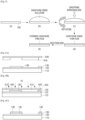
- FIG. 7 illustrates the PCB 100 in a multi-layer structure including the silk screen layer 170, according to an embodiment.
- the electrode forming layer 120 may be formed on both sides of the substrate 110 with a layered structure, and the PSR layer 130 may be formed on the electrode forming layer 120.
- the layered structure on the substrate 110 of the PCB 100 has been already described with reference to FIG. 1 , and will not be further described.
- the silkscreen layer is mainly formed of white color material, and may be formed on the PSR layer 130 and the conductive layer 120.
- characters, numbers, symbols, or the like are written on the PCB to enable easy assembling and better understanding of the circuit. That is, the silkscreen layer 170 may display a position symbol or a region of each element.
- the electronic element 150 is illustrated as being layered on an upper portion of the silk screen layer 170, but the electronic element 150 may be directly connected to the electrode forming layer 120 to form a circuit between the mounted elements. That is, the PSR layer 130, the conductive layer 140, and the silk screen layer 170 may be formed only on a region except the region where the element is to be mounted, and the electronic element 150 may be directly connected to the electrode forming layer 120 in a region where the element is to be mounted.
- FIGS. 8A to 8C are views to describe a method for forming a via hole on the PCB according to an embodiment.
- a punched hole in the PCB generally refers to a blind via hole formed on a surface and a via hole formed in an inside layer in manufacturing a multi-layer PCB.
- the via hole allows an electric signal to be exchanged between an upper surface and a lower surface of an electrode forming layer or between an inner layer and an outer layer.
- a via hole is generally processed by a drilling or punching method on a disk, and then a copper plate is processed on the inner periphery of the via hole so as to have conductivity, and then an insulating ink is filled in an empty space inside the via hole.
- the via hole is formed for electrical connection between each chip or between components in the PCB.
- the via hole may be formed only in a layer where a connection is required without penetrating the surface of the double-sided or multi-layered PCB, thereby enabling application of an electric current with the copper plate layered on the PCB.
- the PCB may connect the conductive layer 140 (or a graphene layer) with the electrode forming layer 120 (or a copper layered plate) through a via hole, in order to increase the efficiency of heat and electrical conductivity of the conductive layer 140.
- FIG. 8A illustrates the PCB 100 disposed innermost layer of the build-up PCB in which the substrate 110 on which ordinary electrode forming layer 120 and the PSR layer 130 are layered is cut into a predetermined standard.
- the PCB has a predetermined standard according to a product on which the PCB is to be mounted.
- a working board may be cut into a square structure of a proper size so as to be suitable for the characteristics of the process.
- FIG. 8B is a view illustrating the via hole 700 being formed on the PCB 100.
- the punching method of the via hole 700 may include melting a surface of the electrode forming layer 120 and the substrate 110 by irradiating a laser beam to one surface of the PCB 100 processed with the PSR layer 130, and evaporating and collecting the melts generated in the process.
- the laser beam may be one obtained by exciting the ground state electrons by applying electrical energy to an oscillator filled with, for example, carbon dioxide to amplify the induced and dissipated light.
- the PSR layer 130 may reduce reflection of the laser beam and increase the absorption rate in the subsequent process, thereby improving roundness of the processed via hole, reducing energy consumption of the laser equipment, and improving the adhesion between the electrode forming layer 120 and the PSR layer 130.
- the via hole 700 may be formed in an area corresponding to a position where the electronic element is to be mounted, in order to efficiently dissipate the heat generated by mounting the electronic element.
- FIG. 8B forming the via hole 700 in an area corresponding to a position where an electronic element is connected to the electrode forming layer 120 and mounted is illustrated as an example, and the via hole 700 may be formed at various positions.
- FIG. 8C is a view illustrating that the conductive layer 140 is formed on the PCB 100 having the via hole 700.
- the conductive layer 140 formed of a conductive material may be formed to be covered on the surface where the via hole is formed, and a plurality of conductive plugs may be provided inside the via hole to dissipate the heat generated in the electronic element to the outside.
- the via hole 700 as illustrated in FIGS. 8B and 8C are blind via holes.
- the blind via holes 820 which are processed by this method has an advantage in that the circuit density may be significantly improved than a through via hole through which the PCB 800 is completely penetrated.
- the via hole may be formed in a form of through via hole so as to connect the substrate 110 and the conductive layer 140 after being layered up to the conductive layer 140, instead of a form of the blind via hole 700.
Landscapes
- Engineering & Computer Science (AREA)
- Microelectronics & Electronic Packaging (AREA)
- Manufacturing & Machinery (AREA)
- Structure Of Printed Boards (AREA)
- Physics & Mathematics (AREA)
- Computer Hardware Design (AREA)
- Power Engineering (AREA)
- Condensed Matter Physics & Semiconductors (AREA)
- General Physics & Mathematics (AREA)
- Electromagnetism (AREA)
- Optics & Photonics (AREA)
- Shielding Devices Or Components To Electric Or Magnetic Fields (AREA)
Claims (8)
- Verfahren zur Herstellung einer Leiterplatte, PCB (100), wobei das Verfahren Folgendes umfasst:Anordnen eines Substrats (110);Bilden einer Elektrodenschicht (120) auf dem Substrat (110);Bilden einer Fotolötstopp-PSR-Schicht (130) in einer strukturierten Weise auf einem ersten Bereich einer Oberseite der Elektrodenschicht (120);Bilden einer leitfähigen Schicht (140) auf der PSR-Schicht (130) in einer strukturierten Weise basierend auf einem Siebdruckverfahren; undMontieren einer Vielzahl von Elementen (150) auf einem zweiten Bereich der Oberseite der Elektrodenschicht (120), wobei sich der zweite Bereich vom ersten Bereich unterscheidet,wobei die leitfähige Schicht (140) ein Graphenfilm ist,wobei die Elektrodenschicht (120) so konfiguriert ist, dass sie durch den zweiten Bereich direkt mit der Vielzahl von Elementen verbunden ist, ohne mit der leitfähigen Schicht (140) verbunden zu sein, undwobei die Vielzahl von Elementen (150) ferner eine oder mehrere Mikro-Leuchtdioden umfasst, die direkt physisch mit der Elektrodenschicht (120) in dem zweiten Bereich verbunden sind, in dem die PSR-Schicht (130) nicht gebildet ist, undwobei eine Höhe der leitfähigen Schicht (140) von der Oberfläche der PCB (100) größer ist als eine Höhe eines oder mehrerer der Vielzahl von Elementen (150) von der Oberfläche der PCB (100).
- Verfahren nach Anspruch 1, ferner umfassend:
Bilden eines Durchgangslochs (700), das die PSR-Schicht (130) durchdringt, um die leitfähige Schicht (140) und die Elektrodenschicht (120) zu verbinden. - Verfahren nach Anspruch 1, wobei das Substrat (110) ein flexibles Material umfasst.
- Verfahren nach Anspruch 1, das ferner Folgendes umfasst:
Verbinden der leitfähigen Schicht (140) mit einer Masseschicht der PCB (100). - Verfahren nach Anspruch 1, das ferner Folgendes umfasst:
Bilden einer zusätzlichen leitfähigen Schicht zum Leiten von Wärme und statischer Elektrizität auf einem dritten Bereich, der sich vom ersten und vom zweiten Bereich unterscheidet. - Leiterplatte, PCB (100), umfassend:ein Substrat (110) zum Anbringen einer Vielzahl von Elementen (150);eine Elektrodenschicht (120), die auf einem Substrat (120) ausgebildet ist;eine Fotolötstopp-PSR-Schicht (130), die in einer gemusterten Weise auf einem ersten Bereich einer Oberseite der Elektrodenschicht (120) ausgebildet ist;eine leitfähige Schicht (140), die in der gemusterten Weise auf der PSR-Schicht ausgebildet ist; undeine Vielzahl von Elementen, die auf einem zweiten Bereich der Oberseite der Elektrodenschicht angebracht sind,wobei die leitfähige Schicht ein Graphenfilm ist,wobei die Elektrodenschicht so konfiguriert ist, dass sie durch den zweiten Bereich direkt mit der Vielzahl von Elementen verbunden werden kann, ohne mit der leitfähigen Schicht verbunden zu sein, undwobei die Vielzahl von Elementen ferner eine oder mehrere Mikro-Leuchtdioden umfasst, die direkt physikalisch mit der Elektrodenschicht in dem zweiten Bereich verbunden sind, in dem die PSR-Schicht nicht gebildet ist, undwobei eine Höhe der leitfähigen Schicht (140) von der Oberfläche der PCB (100) größer ist als eine Höhe eines oder mehrerer der Vielzahl von Elementen (160) von der Oberfläche der PCB (100),wobei die leitfähige Schicht (140) auf der Grundlage eines Siebdruckverfahrens gebildet wird.
- PCB (100) nach Anspruch 6, ferner umfassend:
ein Durchgangsloch (700), das die PSR-Schicht (130) durchdringt, um die leitfähige Schicht (140) und die Elektrodenschicht (120) zu verbinden. - PCB (100) nach Anspruch 6, wobei das Substrat (110) ein flexibles Material umfasst.
Applications Claiming Priority (2)
| Application Number | Priority Date | Filing Date | Title |
|---|---|---|---|
| KR1020180068362A KR102344359B1 (ko) | 2018-06-14 | 2018-06-14 | 인쇄회로기판과 그 제조 방법 |
| PCT/KR2019/006877 WO2019240435A1 (en) | 2018-06-14 | 2019-06-07 | Printed circuit board and manufacturing method thereof |
Publications (4)
| Publication Number | Publication Date |
|---|---|
| EP3763174A1 EP3763174A1 (de) | 2021-01-13 |
| EP3763174A4 EP3763174A4 (de) | 2021-04-21 |
| EP3763174B1 true EP3763174B1 (de) | 2024-10-23 |
| EP3763174C0 EP3763174C0 (de) | 2024-10-23 |
Family
ID=68840581
Family Applications (1)
| Application Number | Title | Priority Date | Filing Date |
|---|---|---|---|
| EP19820407.5A Active EP3763174B1 (de) | 2018-06-14 | 2019-06-07 | Leiterplatte und herstellungsverfahren dafür |
Country Status (5)
| Country | Link |
|---|---|
| US (2) | US11039532B2 (de) |
| EP (1) | EP3763174B1 (de) |
| KR (1) | KR102344359B1 (de) |
| ES (1) | ES2992446T3 (de) |
| WO (1) | WO2019240435A1 (de) |
Families Citing this family (1)
| Publication number | Priority date | Publication date | Assignee | Title |
|---|---|---|---|---|
| CN108987426B (zh) * | 2018-07-23 | 2020-09-29 | 上海天马微电子有限公司 | 一种柔性led显示面板及电子设备 |
Family Cites Families (20)
| Publication number | Priority date | Publication date | Assignee | Title |
|---|---|---|---|---|
| JPH05183291A (ja) * | 1991-12-27 | 1993-07-23 | Japan Metals & Chem Co Ltd | Emiシールドプリント配線板の製造方法 |
| JP2643113B2 (ja) * | 1995-03-13 | 1997-08-20 | 日本電気株式会社 | プリント配線基板 |
| EP1959506A2 (de) * | 1997-01-31 | 2008-08-20 | Matsushita Electric Industrial Co., Ltd. | Herstellungsverfahren für eine lichtemittierende Halbleitervorrichtung |
| JP3870947B2 (ja) * | 2001-07-02 | 2007-01-24 | 松下電器産業株式会社 | 弾性表面波装置の製造方法 |
| KR101059576B1 (ko) | 2005-11-02 | 2011-08-26 | 자화전자(주) | 조명용 엘이디 기판 및 조명 유닛 |
| US8172097B2 (en) | 2005-11-10 | 2012-05-08 | Daktronics, Inc. | LED display module |
| JP5080295B2 (ja) * | 2007-01-26 | 2012-11-21 | 帝人株式会社 | 放熱性実装基板およびその製造方法 |
| JP2009253098A (ja) | 2008-04-08 | 2009-10-29 | Mitsubishi Electric Corp | Led表示装置 |
| EP2353179A4 (de) * | 2008-10-17 | 2012-10-03 | Occam Portfolio Llc | Flexible schaltbaugruppen ohne lötung und herstellungsverfahren dafür |
| KR101109239B1 (ko) * | 2009-10-19 | 2012-01-30 | 삼성전기주식회사 | 방열기판 |
| KR101042441B1 (ko) | 2010-10-13 | 2011-06-16 | 백선영 | 칩led 전광모듈 |
| KR101766462B1 (ko) * | 2010-12-22 | 2017-08-08 | 엘지이노텍 주식회사 | 인쇄회로기판 |
| KR101958008B1 (ko) | 2011-06-17 | 2019-03-15 | 엘지디스플레이 주식회사 | 유기전계발광표시장치 |
| WO2013073873A1 (ko) * | 2011-11-16 | 2013-05-23 | Seong Nak Hoon | 선광원 발생장치와, 선광원 발생장치를 구비한 노광기와, 선광원 발생장치에 사용되는 렌티큐라시스템 |
| KR102048053B1 (ko) * | 2013-02-26 | 2019-11-25 | 삼성디스플레이 주식회사 | 윈도우 부재 및 이를 구비하는 표시 장치 |
| US8987765B2 (en) * | 2013-06-17 | 2015-03-24 | LuxVue Technology Corporation | Reflective bank structure and method for integrating a light emitting device |
| KR101412617B1 (ko) | 2013-07-05 | 2014-06-27 | 홍철한 | 전자파 흡수 및 방열 특성을 가지는 led용 pcb 및 그 제조방법 |
| CN103545053B (zh) * | 2013-10-25 | 2016-03-09 | 深圳市华星光电技术有限公司 | 透明导电薄膜的制备方法及具有该导电薄膜的cf基板的制备方法 |
| KR20160004158A (ko) * | 2014-07-02 | 2016-01-12 | 삼성전기주식회사 | 패키지 기판 |
| CN112331623B (zh) * | 2017-12-15 | 2024-09-20 | 光宝科技股份有限公司 | 发光二极管封装结构及散热基板 |
-
2018
- 2018-06-14 KR KR1020180068362A patent/KR102344359B1/ko active Active
-
2019
- 2019-06-07 ES ES19820407T patent/ES2992446T3/es active Active
- 2019-06-07 EP EP19820407.5A patent/EP3763174B1/de active Active
- 2019-06-07 WO PCT/KR2019/006877 patent/WO2019240435A1/en not_active Ceased
- 2019-06-12 US US16/439,207 patent/US11039532B2/en active Active
-
2021
- 2021-05-13 US US17/319,633 patent/US11792924B2/en active Active
Also Published As
| Publication number | Publication date |
|---|---|
| US20210282262A1 (en) | 2021-09-09 |
| WO2019240435A1 (en) | 2019-12-19 |
| ES2992446T3 (es) | 2024-12-12 |
| US20190387620A1 (en) | 2019-12-19 |
| EP3763174A4 (de) | 2021-04-21 |
| KR20190141504A (ko) | 2019-12-24 |
| KR102344359B1 (ko) | 2021-12-29 |
| EP3763174C0 (de) | 2024-10-23 |
| US11039532B2 (en) | 2021-06-15 |
| US11792924B2 (en) | 2023-10-17 |
| EP3763174A1 (de) | 2021-01-13 |
Similar Documents
| Publication | Publication Date | Title |
|---|---|---|
| US6970219B1 (en) | Flexible display and method of making the same | |
| EP1498013B1 (de) | Flexible zwischenschaltungsstrukturen für elektrische geräte und lichtquellen mit derartigen strukturen | |
| US20140190727A1 (en) | Method of fabricating flexible metal core printed circuit board | |
| US7253449B2 (en) | Light source module of light emitting diode | |
| TWI646873B (zh) | 電子裝置與其製造方法 | |
| US10312223B2 (en) | Semiconductor light-emitting device and method for producing the same | |
| US20080062657A1 (en) | Multi-layed printed circuit board having integrated circuit embedded therein | |
| US11792924B2 (en) | Printed circuit board and manufacturing method thereof | |
| US11094740B2 (en) | Backboard, display device, and method for fabricating backboard | |
| US8773859B2 (en) | Driver package | |
| KR20120130640A (ko) | 양면 연성 인쇄회로기판 및 그 제조방법 | |
| JP6610497B2 (ja) | 電子装置およびその製造方法 | |
| TWI740579B (zh) | 電路板及其製備方法、背光板 | |
| CN110418491A (zh) | 电路板及光学装置 | |
| TWM553882U (zh) | 發光二極體顯示裝置 | |
| KR20110133244A (ko) | 엘이디 어레이 방법, 이에 사용되는 기판과 이를 사용한 엘이디 어레이 패키지 | |
| JP2006500607A (ja) | 電子回路・ディスプレイ製作のプリンタおよび方法 | |
| KR100660126B1 (ko) | 방열판 구조를 가진 회로 기판 | |
| KR100775449B1 (ko) | 방열층 구조를 가진 회로 기판 | |
| JP2006216735A (ja) | 電子部品実装基板 | |
| KR20150072814A (ko) | 방열판 일체형 led 모듈 | |
| US20060202224A1 (en) | Substrate structure for light-emitting diode module | |
| KR101376750B1 (ko) | 연성 인쇄회로기판 및 그 제조방법 | |
| KR101008963B1 (ko) | 전자잉크층을 이용한 디스플레이 장치 | |
| US20160295684A1 (en) | Printed circuit board and method of fabricating the same |
Legal Events
| Date | Code | Title | Description |
|---|---|---|---|
| STAA | Information on the status of an ep patent application or granted ep patent |
Free format text: STATUS: THE INTERNATIONAL PUBLICATION HAS BEEN MADE |
|
| PUAI | Public reference made under article 153(3) epc to a published international application that has entered the european phase |
Free format text: ORIGINAL CODE: 0009012 |
|
| STAA | Information on the status of an ep patent application or granted ep patent |
Free format text: STATUS: REQUEST FOR EXAMINATION WAS MADE |
|
| 17P | Request for examination filed |
Effective date: 20201008 |
|
| AK | Designated contracting states |
Kind code of ref document: A1 Designated state(s): AL AT BE BG CH CY CZ DE DK EE ES FI FR GB GR HR HU IE IS IT LI LT LU LV MC MK MT NL NO PL PT RO RS SE SI SK SM TR |
|
| AX | Request for extension of the european patent |
Extension state: BA ME |
|
| A4 | Supplementary search report drawn up and despatched |
Effective date: 20210318 |
|
| RIC1 | Information provided on ipc code assigned before grant |
Ipc: H05K 3/34 20060101ALI20210312BHEP Ipc: H05K 1/02 20060101AFI20210312BHEP |
|
| DAV | Request for validation of the european patent (deleted) | ||
| DAX | Request for extension of the european patent (deleted) | ||
| STAA | Information on the status of an ep patent application or granted ep patent |
Free format text: STATUS: EXAMINATION IS IN PROGRESS |
|
| 17Q | First examination report despatched |
Effective date: 20220926 |
|
| REG | Reference to a national code |
Ref country code: DE Ref legal event code: R079 Free format text: PREVIOUS MAIN CLASS: H05K0003120000 Ipc: H05K0001180000 Ref country code: DE Ref legal event code: R079 Ref document number: 602019060868 Country of ref document: DE Free format text: PREVIOUS MAIN CLASS: H05K0003120000 Ipc: H05K0001180000 |
|
| RIC1 | Information provided on ipc code assigned before grant |
Ipc: H01L 25/075 20060101ALN20240709BHEP Ipc: H05K 3/12 20060101ALN20240709BHEP Ipc: H01L 23/00 20060101ALI20240709BHEP Ipc: H01L 23/498 20060101ALI20240709BHEP Ipc: H01L 21/48 20060101ALI20240709BHEP Ipc: H05K 3/34 20060101ALI20240709BHEP Ipc: H05K 1/18 20060101AFI20240709BHEP |
|
| GRAP | Despatch of communication of intention to grant a patent |
Free format text: ORIGINAL CODE: EPIDOSNIGR1 |
|
| STAA | Information on the status of an ep patent application or granted ep patent |
Free format text: STATUS: GRANT OF PATENT IS INTENDED |
|
| RIC1 | Information provided on ipc code assigned before grant |
Ipc: H01L 25/075 20060101ALN20240719BHEP Ipc: H05K 3/12 20060101ALN20240719BHEP Ipc: H01L 23/00 20060101ALI20240719BHEP Ipc: H01L 23/498 20060101ALI20240719BHEP Ipc: H01L 21/48 20060101ALI20240719BHEP Ipc: H05K 3/34 20060101ALI20240719BHEP Ipc: H05K 1/18 20060101AFI20240719BHEP |
|
| GRAS | Grant fee paid |
Free format text: ORIGINAL CODE: EPIDOSNIGR3 |
|
| GRAA | (expected) grant |
Free format text: ORIGINAL CODE: 0009210 |
|
| STAA | Information on the status of an ep patent application or granted ep patent |
Free format text: STATUS: THE PATENT HAS BEEN GRANTED |
|
| INTG | Intention to grant announced |
Effective date: 20240822 |
|
| AK | Designated contracting states |
Kind code of ref document: B1 Designated state(s): AL AT BE BG CH CY CZ DE DK EE ES FI FR GB GR HR HU IE IS IT LI LT LU LV MC MK MT NL NO PL PT RO RS SE SI SK SM TR |
|
| REG | Reference to a national code |
Ref country code: GB Ref legal event code: FG4D |
|
| REG | Reference to a national code |
Ref country code: CH Ref legal event code: EP |
|
| REG | Reference to a national code |
Ref country code: DE Ref legal event code: R096 Ref document number: 602019060868 Country of ref document: DE |
|
| REG | Reference to a national code |
Ref country code: IE Ref legal event code: FG4D |
|
| REG | Reference to a national code |
Ref country code: ES Ref legal event code: FG2A Ref document number: 2992446 Country of ref document: ES Kind code of ref document: T3 Effective date: 20241212 |
|
| U01 | Request for unitary effect filed |
Effective date: 20241114 |
|
| U07 | Unitary effect registered |
Designated state(s): AT BE BG DE DK EE FI FR IT LT LU LV MT NL PT RO SE SI Effective date: 20241120 |
|
| PG25 | Lapsed in a contracting state [announced via postgrant information from national office to epo] |
Ref country code: IS Free format text: LAPSE BECAUSE OF FAILURE TO SUBMIT A TRANSLATION OF THE DESCRIPTION OR TO PAY THE FEE WITHIN THE PRESCRIBED TIME-LIMIT Effective date: 20250223 Ref country code: HR Free format text: LAPSE BECAUSE OF FAILURE TO SUBMIT A TRANSLATION OF THE DESCRIPTION OR TO PAY THE FEE WITHIN THE PRESCRIBED TIME-LIMIT Effective date: 20241023 |
|
| PG25 | Lapsed in a contracting state [announced via postgrant information from national office to epo] |
Ref country code: NO Free format text: LAPSE BECAUSE OF FAILURE TO SUBMIT A TRANSLATION OF THE DESCRIPTION OR TO PAY THE FEE WITHIN THE PRESCRIBED TIME-LIMIT Effective date: 20250123 |
|
| PG25 | Lapsed in a contracting state [announced via postgrant information from national office to epo] |
Ref country code: GR Free format text: LAPSE BECAUSE OF FAILURE TO SUBMIT A TRANSLATION OF THE DESCRIPTION OR TO PAY THE FEE WITHIN THE PRESCRIBED TIME-LIMIT Effective date: 20250124 |
|
| PG25 | Lapsed in a contracting state [announced via postgrant information from national office to epo] |
Ref country code: PL Free format text: LAPSE BECAUSE OF FAILURE TO SUBMIT A TRANSLATION OF THE DESCRIPTION OR TO PAY THE FEE WITHIN THE PRESCRIBED TIME-LIMIT Effective date: 20241023 |
|
| PG25 | Lapsed in a contracting state [announced via postgrant information from national office to epo] |
Ref country code: RS Free format text: LAPSE BECAUSE OF FAILURE TO SUBMIT A TRANSLATION OF THE DESCRIPTION OR TO PAY THE FEE WITHIN THE PRESCRIBED TIME-LIMIT Effective date: 20250123 |
|
| PG25 | Lapsed in a contracting state [announced via postgrant information from national office to epo] |
Ref country code: SM Free format text: LAPSE BECAUSE OF FAILURE TO SUBMIT A TRANSLATION OF THE DESCRIPTION OR TO PAY THE FEE WITHIN THE PRESCRIBED TIME-LIMIT Effective date: 20241023 |
|
| PGFP | Annual fee paid to national office [announced via postgrant information from national office to epo] |
Ref country code: GB Payment date: 20250520 Year of fee payment: 7 |
|
| PG25 | Lapsed in a contracting state [announced via postgrant information from national office to epo] |
Ref country code: SK Free format text: LAPSE BECAUSE OF FAILURE TO SUBMIT A TRANSLATION OF THE DESCRIPTION OR TO PAY THE FEE WITHIN THE PRESCRIBED TIME-LIMIT Effective date: 20241023 |
|
| PG25 | Lapsed in a contracting state [announced via postgrant information from national office to epo] |
Ref country code: CZ Free format text: LAPSE BECAUSE OF FAILURE TO SUBMIT A TRANSLATION OF THE DESCRIPTION OR TO PAY THE FEE WITHIN THE PRESCRIBED TIME-LIMIT Effective date: 20241023 |
|
| U20 | Renewal fee for the european patent with unitary effect paid |
Year of fee payment: 7 Effective date: 20250624 |
|
| PLBE | No opposition filed within time limit |
Free format text: ORIGINAL CODE: 0009261 |
|
| STAA | Information on the status of an ep patent application or granted ep patent |
Free format text: STATUS: NO OPPOSITION FILED WITHIN TIME LIMIT |
|
| 26N | No opposition filed |
Effective date: 20250724 |
|
| PGFP | Annual fee paid to national office [announced via postgrant information from national office to epo] |
Ref country code: ES Payment date: 20250714 Year of fee payment: 7 |
|
| REG | Reference to a national code |
Ref country code: CH Ref legal event code: H13 Free format text: ST27 STATUS EVENT CODE: U-0-0-H10-H13 (AS PROVIDED BY THE NATIONAL OFFICE) Effective date: 20260127 |
|
| PG25 | Lapsed in a contracting state [announced via postgrant information from national office to epo] |
Ref country code: MC Free format text: LAPSE BECAUSE OF FAILURE TO SUBMIT A TRANSLATION OF THE DESCRIPTION OR TO PAY THE FEE WITHIN THE PRESCRIBED TIME-LIMIT Effective date: 20241023 |