EP3761084A1 - Polarisationsfolienlaminat für ein angetriebenes fahrzeug und optische anzeigetafel, in der das polarisationsfolienlaminat verwendet wird - Google Patents
Polarisationsfolienlaminat für ein angetriebenes fahrzeug und optische anzeigetafel, in der das polarisationsfolienlaminat verwendet wird Download PDFInfo
- Publication number
- EP3761084A1 EP3761084A1 EP19760588.4A EP19760588A EP3761084A1 EP 3761084 A1 EP3761084 A1 EP 3761084A1 EP 19760588 A EP19760588 A EP 19760588A EP 3761084 A1 EP3761084 A1 EP 3761084A1
- Authority
- EP
- European Patent Office
- Prior art keywords
- polarizing film
- coordinate point
- water content
- film laminate
- iodine concentration
- Prior art date
- Legal status (The legal status is an assumption and is not a legal conclusion. Google has not performed a legal analysis and makes no representation as to the accuracy of the status listed.)
- Withdrawn
Links
- 230000003287 optical effect Effects 0.000 title claims description 62
- XLYOFNOQVPJJNP-UHFFFAOYSA-N water Substances O XLYOFNOQVPJJNP-UHFFFAOYSA-N 0.000 claims abstract description 196
- ZCYVEMRRCGMTRW-UHFFFAOYSA-N 7553-56-2 Chemical compound [I] ZCYVEMRRCGMTRW-UHFFFAOYSA-N 0.000 claims abstract description 156
- 229910052740 iodine Inorganic materials 0.000 claims abstract description 155
- 239000011630 iodine Substances 0.000 claims abstract description 155
- 239000010408 film Substances 0.000 claims description 643
- 239000010410 layer Substances 0.000 claims description 179
- 239000004372 Polyvinyl alcohol Substances 0.000 claims description 103
- 229920002451 polyvinyl alcohol Polymers 0.000 claims description 103
- 239000004973 liquid crystal related substance Substances 0.000 claims description 64
- 230000008859 change Effects 0.000 claims description 58
- 229920005989 resin Polymers 0.000 claims description 50
- 239000011347 resin Substances 0.000 claims description 50
- 210000002858 crystal cell Anatomy 0.000 claims description 48
- 230000003667 anti-reflective effect Effects 0.000 claims description 46
- 238000002834 transmittance Methods 0.000 claims description 46
- 239000000758 substrate Substances 0.000 claims description 36
- 230000035699 permeability Effects 0.000 claims description 34
- 238000010438 heat treatment Methods 0.000 claims description 32
- 239000012788 optical film Substances 0.000 claims description 30
- 229910052725 zinc Inorganic materials 0.000 claims description 21
- 239000011701 zinc Substances 0.000 claims description 21
- HCHKCACWOHOZIP-UHFFFAOYSA-N Zinc Chemical compound [Zn] HCHKCACWOHOZIP-UHFFFAOYSA-N 0.000 claims description 20
- 210000004027 cell Anatomy 0.000 claims description 20
- 239000004820 Pressure-sensitive adhesive Substances 0.000 claims description 19
- 238000010521 absorption reaction Methods 0.000 claims description 14
- 239000011521 glass Substances 0.000 claims description 11
- 230000005684 electric field Effects 0.000 claims description 7
- 239000012790 adhesive layer Substances 0.000 claims description 5
- 230000015572 biosynthetic process Effects 0.000 abstract description 53
- 150000004291 polyenes Chemical class 0.000 abstract description 44
- 238000002845 discoloration Methods 0.000 abstract description 34
- 238000000034 method Methods 0.000 description 102
- 230000008569 process Effects 0.000 description 86
- 239000000853 adhesive Substances 0.000 description 55
- 230000001070 adhesive effect Effects 0.000 description 55
- NLKNQRATVPKPDG-UHFFFAOYSA-M potassium iodide Chemical compound [K+].[I-] NLKNQRATVPKPDG-UHFFFAOYSA-M 0.000 description 54
- 150000001875 compounds Chemical class 0.000 description 48
- 239000007864 aqueous solution Substances 0.000 description 47
- 238000004519 manufacturing process Methods 0.000 description 47
- 230000000052 comparative effect Effects 0.000 description 41
- 238000001035 drying Methods 0.000 description 41
- 238000004043 dyeing Methods 0.000 description 40
- 239000000243 solution Substances 0.000 description 40
- NIXOWILDQLNWCW-UHFFFAOYSA-M Acrylate Chemical compound [O-]C(=O)C=C NIXOWILDQLNWCW-UHFFFAOYSA-M 0.000 description 36
- DKNPRRRKHAEUMW-UHFFFAOYSA-N Iodine aqueous Chemical compound [K+].I[I-]I DKNPRRRKHAEUMW-UHFFFAOYSA-N 0.000 description 25
- 238000007654 immersion Methods 0.000 description 24
- QAOWNCQODCNURD-UHFFFAOYSA-L Sulfate Chemical compound [O-]S([O-])(=O)=O QAOWNCQODCNURD-UHFFFAOYSA-L 0.000 description 21
- 230000001681 protective effect Effects 0.000 description 18
- HRPVXLWXLXDGHG-UHFFFAOYSA-N Acrylamide Chemical compound NC(=O)C=C HRPVXLWXLXDGHG-UHFFFAOYSA-N 0.000 description 17
- 239000000463 material Substances 0.000 description 17
- 238000005406 washing Methods 0.000 description 16
- 229940117913 acrylamide Drugs 0.000 description 15
- KGBXLFKZBHKPEV-UHFFFAOYSA-N boric acid Chemical compound OB(O)O KGBXLFKZBHKPEV-UHFFFAOYSA-N 0.000 description 15
- 235000010338 boric acid Nutrition 0.000 description 15
- 229960002645 boric acid Drugs 0.000 description 15
- 239000004327 boric acid Substances 0.000 description 14
- 238000004544 sputter deposition Methods 0.000 description 13
- 238000004132 cross linking Methods 0.000 description 12
- 239000002904 solvent Substances 0.000 description 12
- 238000012360 testing method Methods 0.000 description 12
- 239000010409 thin film Substances 0.000 description 12
- -1 triglycerin Chemical compound 0.000 description 12
- 229920000139 polyethylene terephthalate Polymers 0.000 description 11
- 239000005020 polyethylene terephthalate Substances 0.000 description 11
- NIXOWILDQLNWCW-UHFFFAOYSA-N 2-Propenoic acid Natural products OC(=O)C=C NIXOWILDQLNWCW-UHFFFAOYSA-N 0.000 description 10
- 150000003926 acrylamides Chemical class 0.000 description 10
- 230000007423 decrease Effects 0.000 description 10
- 238000005470 impregnation Methods 0.000 description 10
- 229910052751 metal Inorganic materials 0.000 description 10
- 239000002184 metal Substances 0.000 description 10
- 229920002284 Cellulose triacetate Polymers 0.000 description 9
- RRHGJUQNOFWUDK-UHFFFAOYSA-N Isoprene Chemical compound CC(=C)C=C RRHGJUQNOFWUDK-UHFFFAOYSA-N 0.000 description 9
- NNLVGZFZQQXQNW-ADJNRHBOSA-N [(2r,3r,4s,5r,6s)-4,5-diacetyloxy-3-[(2s,3r,4s,5r,6r)-3,4,5-triacetyloxy-6-(acetyloxymethyl)oxan-2-yl]oxy-6-[(2r,3r,4s,5r,6s)-4,5,6-triacetyloxy-2-(acetyloxymethyl)oxan-3-yl]oxyoxan-2-yl]methyl acetate Chemical compound O([C@@H]1O[C@@H]([C@H]([C@H](OC(C)=O)[C@H]1OC(C)=O)O[C@H]1[C@@H]([C@@H](OC(C)=O)[C@H](OC(C)=O)[C@@H](COC(C)=O)O1)OC(C)=O)COC(=O)C)[C@@H]1[C@@H](COC(C)=O)O[C@@H](OC(C)=O)[C@H](OC(C)=O)[C@H]1OC(C)=O NNLVGZFZQQXQNW-ADJNRHBOSA-N 0.000 description 9
- 238000010586 diagram Methods 0.000 description 9
- 238000011088 calibration curve Methods 0.000 description 8
- 150000001925 cycloalkenes Chemical class 0.000 description 8
- 238000000605 extraction Methods 0.000 description 8
- 239000000178 monomer Substances 0.000 description 8
- 239000002245 particle Substances 0.000 description 8
- 229920000058 polyacrylate Polymers 0.000 description 8
- 238000006116 polymerization reaction Methods 0.000 description 8
- 239000000654 additive Substances 0.000 description 7
- 125000003700 epoxy group Chemical group 0.000 description 7
- 239000007787 solid Substances 0.000 description 7
- 230000008961 swelling Effects 0.000 description 7
- ZWEHNKRNPOVVGH-UHFFFAOYSA-N 2-Butanone Chemical compound CCC(C)=O ZWEHNKRNPOVVGH-UHFFFAOYSA-N 0.000 description 6
- YMWUJEATGCHHMB-UHFFFAOYSA-N Dichloromethane Chemical compound ClCCl YMWUJEATGCHHMB-UHFFFAOYSA-N 0.000 description 6
- XEKOWRVHYACXOJ-UHFFFAOYSA-N Ethyl acetate Chemical compound CCOC(C)=O XEKOWRVHYACXOJ-UHFFFAOYSA-N 0.000 description 6
- CERQOIWHTDAKMF-UHFFFAOYSA-N Methacrylic acid Chemical compound CC(=C)C(O)=O CERQOIWHTDAKMF-UHFFFAOYSA-N 0.000 description 6
- VYPSYNLAJGMNEJ-UHFFFAOYSA-N Silicium dioxide Chemical compound O=[Si]=O VYPSYNLAJGMNEJ-UHFFFAOYSA-N 0.000 description 6
- 125000002091 cationic group Chemical group 0.000 description 6
- 238000000576 coating method Methods 0.000 description 6
- 239000003431 cross linking reagent Substances 0.000 description 6
- 238000011156 evaluation Methods 0.000 description 6
- 150000002596 lactones Chemical group 0.000 description 6
- 238000005259 measurement Methods 0.000 description 6
- 239000011241 protective layer Substances 0.000 description 6
- 150000003254 radicals Chemical class 0.000 description 6
- 150000003751 zinc Chemical class 0.000 description 6
- LYCAIKOWRPUZTN-UHFFFAOYSA-N Ethylene glycol Chemical compound OCCO LYCAIKOWRPUZTN-UHFFFAOYSA-N 0.000 description 5
- 230000015556 catabolic process Effects 0.000 description 5
- 239000003795 chemical substances by application Substances 0.000 description 5
- 238000006731 degradation reaction Methods 0.000 description 5
- XMBWDFGMSWQBCA-UHFFFAOYSA-N hydrogen iodide Chemical compound I XMBWDFGMSWQBCA-UHFFFAOYSA-N 0.000 description 5
- 238000010030 laminating Methods 0.000 description 5
- 239000004014 plasticizer Substances 0.000 description 5
- 229920002554 vinyl polymer Polymers 0.000 description 5
- NWONKYPBYAMBJT-UHFFFAOYSA-L zinc sulfate Chemical compound [Zn+2].[O-]S([O-])(=O)=O NWONKYPBYAMBJT-UHFFFAOYSA-L 0.000 description 5
- 229960001763 zinc sulfate Drugs 0.000 description 5
- 229910000368 zinc sulfate Inorganic materials 0.000 description 5
- KBPLFHHGFOOTCA-UHFFFAOYSA-N 1-Octanol Chemical compound CCCCCCCCO KBPLFHHGFOOTCA-UHFFFAOYSA-N 0.000 description 4
- 239000004925 Acrylic resin Substances 0.000 description 4
- 229920000178 Acrylic resin Polymers 0.000 description 4
- PEDCQBHIVMGVHV-UHFFFAOYSA-N Glycerine Chemical compound OCC(O)CO PEDCQBHIVMGVHV-UHFFFAOYSA-N 0.000 description 4
- 239000006087 Silane Coupling Agent Substances 0.000 description 4
- 230000000996 additive effect Effects 0.000 description 4
- IISBACLAFKSPIT-UHFFFAOYSA-N bisphenol A Chemical compound C=1C=C(O)C=CC=1C(C)(C)C1=CC=C(O)C=C1 IISBACLAFKSPIT-UHFFFAOYSA-N 0.000 description 4
- 238000002347 injection Methods 0.000 description 4
- 239000007924 injection Substances 0.000 description 4
- 238000007127 saponification reaction Methods 0.000 description 4
- 239000000126 substance Substances 0.000 description 4
- 125000000391 vinyl group Chemical group [H]C([*])=C([H])[H] 0.000 description 4
- JIAARYAFYJHUJI-UHFFFAOYSA-L zinc dichloride Chemical compound [Cl-].[Cl-].[Zn+2] JIAARYAFYJHUJI-UHFFFAOYSA-L 0.000 description 4
- XLPJNCYCZORXHG-UHFFFAOYSA-N 1-morpholin-4-ylprop-2-en-1-one Chemical compound C=CC(=O)N1CCOCC1 XLPJNCYCZORXHG-UHFFFAOYSA-N 0.000 description 3
- VNGLVZLEUDIDQH-UHFFFAOYSA-N 4-[2-(4-hydroxyphenyl)propan-2-yl]phenol;2-methyloxirane Chemical compound CC1CO1.C=1C=C(O)C=CC=1C(C)(C)C1=CC=C(O)C=C1 VNGLVZLEUDIDQH-UHFFFAOYSA-N 0.000 description 3
- IJGRMHOSHXDMSA-UHFFFAOYSA-N Atomic nitrogen Chemical compound N#N IJGRMHOSHXDMSA-UHFFFAOYSA-N 0.000 description 3
- 239000004593 Epoxy Substances 0.000 description 3
- VZCYOOQTPOCHFL-OWOJBTEDSA-N Fumaric acid Chemical compound OC(=O)\C=C\C(O)=O VZCYOOQTPOCHFL-OWOJBTEDSA-N 0.000 description 3
- ZLMJMSJWJFRBEC-UHFFFAOYSA-N Potassium Chemical compound [K] ZLMJMSJWJFRBEC-UHFFFAOYSA-N 0.000 description 3
- DNIAPMSPPWPWGF-UHFFFAOYSA-N Propylene glycol Chemical compound CC(O)CO DNIAPMSPPWPWGF-UHFFFAOYSA-N 0.000 description 3
- ZJCCRDAZUWHFQH-UHFFFAOYSA-N Trimethylolpropane Chemical compound CCC(CO)(CO)CO ZJCCRDAZUWHFQH-UHFFFAOYSA-N 0.000 description 3
- 239000002253 acid Substances 0.000 description 3
- 125000002723 alicyclic group Chemical group 0.000 description 3
- 125000003118 aryl group Chemical group 0.000 description 3
- 238000006243 chemical reaction Methods 0.000 description 3
- 239000011248 coating agent Substances 0.000 description 3
- 230000001186 cumulative effect Effects 0.000 description 3
- 125000004122 cyclic group Chemical group 0.000 description 3
- 150000002500 ions Chemical class 0.000 description 3
- QQVIHTHCMHWDBS-UHFFFAOYSA-N isophthalic acid Chemical compound OC(=O)C1=CC=CC(C(O)=O)=C1 QQVIHTHCMHWDBS-UHFFFAOYSA-N 0.000 description 3
- 230000002093 peripheral effect Effects 0.000 description 3
- 229920000515 polycarbonate Polymers 0.000 description 3
- 239000004417 polycarbonate Substances 0.000 description 3
- 239000003505 polymerization initiator Substances 0.000 description 3
- 229920005672 polyolefin resin Polymers 0.000 description 3
- 229910052700 potassium Inorganic materials 0.000 description 3
- 239000011591 potassium Substances 0.000 description 3
- 239000012266 salt solution Substances 0.000 description 3
- 229920006395 saturated elastomer Polymers 0.000 description 3
- 229910052814 silicon oxide Inorganic materials 0.000 description 3
- FVAUCKIRQBBSSJ-UHFFFAOYSA-M sodium iodide Chemical compound [Na+].[I-] FVAUCKIRQBBSSJ-UHFFFAOYSA-M 0.000 description 3
- 229920005992 thermoplastic resin Polymers 0.000 description 3
- VZCYOOQTPOCHFL-UHFFFAOYSA-N trans-butenedioic acid Natural products OC(=O)C=CC(O)=O VZCYOOQTPOCHFL-UHFFFAOYSA-N 0.000 description 3
- LDHQCZJRKDOVOX-UHFFFAOYSA-N trans-crotonic acid Natural products CC=CC(O)=O LDHQCZJRKDOVOX-UHFFFAOYSA-N 0.000 description 3
- ALVZNPYWJMLXKV-UHFFFAOYSA-N 1,9-Nonanediol Chemical compound OCCCCCCCCCO ALVZNPYWJMLXKV-UHFFFAOYSA-N 0.000 description 2
- RHNJVKIVSXGYBD-UHFFFAOYSA-N 10-prop-2-enoyloxydecyl prop-2-enoate Chemical compound C=CC(=O)OCCCCCCCCCCOC(=O)C=C RHNJVKIVSXGYBD-UHFFFAOYSA-N 0.000 description 2
- TXBCBTDQIULDIA-UHFFFAOYSA-N 2-[[3-hydroxy-2,2-bis(hydroxymethyl)propoxy]methyl]-2-(hydroxymethyl)propane-1,3-diol Chemical compound OCC(CO)(CO)COCC(CO)(CO)CO TXBCBTDQIULDIA-UHFFFAOYSA-N 0.000 description 2
- KANZWHBYRHQMKZ-UHFFFAOYSA-N 2-ethenylpyrazine Chemical compound C=CC1=CN=CC=N1 KANZWHBYRHQMKZ-UHFFFAOYSA-N 0.000 description 2
- WVQHODUGKTXKQF-UHFFFAOYSA-N 2-ethyl-2-methylhexane-1,1-diol Chemical compound CCCCC(C)(CC)C(O)O WVQHODUGKTXKQF-UHFFFAOYSA-N 0.000 description 2
- LZFNKJKBRGFWDU-UHFFFAOYSA-N 3,6-dioxabicyclo[6.3.1]dodeca-1(12),8,10-triene-2,7-dione Chemical group O=C1OCCOC(=O)C2=CC=CC1=C2 LZFNKJKBRGFWDU-UHFFFAOYSA-N 0.000 description 2
- WPSWDCBWMRJJED-UHFFFAOYSA-N 4-[2-(4-hydroxyphenyl)propan-2-yl]phenol;oxirane Chemical compound C1CO1.C=1C=C(O)C=CC=1C(C)(C)C1=CC=C(O)C=C1 WPSWDCBWMRJJED-UHFFFAOYSA-N 0.000 description 2
- OMPJBNCRMGITSC-UHFFFAOYSA-N Benzoylperoxide Chemical compound C=1C=CC=CC=1C(=O)OOC(=O)C1=CC=CC=C1 OMPJBNCRMGITSC-UHFFFAOYSA-N 0.000 description 2
- XDTMQSROBMDMFD-UHFFFAOYSA-N Cyclohexane Chemical compound C1CCCCC1 XDTMQSROBMDMFD-UHFFFAOYSA-N 0.000 description 2
- LFQSCWFLJHTTHZ-UHFFFAOYSA-N Ethanol Chemical compound CCO LFQSCWFLJHTTHZ-UHFFFAOYSA-N 0.000 description 2
- XEEYBQQBJWHFJM-UHFFFAOYSA-N Iron Chemical compound [Fe] XEEYBQQBJWHFJM-UHFFFAOYSA-N 0.000 description 2
- PXHVJJICTQNCMI-UHFFFAOYSA-N Nickel Chemical compound [Ni] PXHVJJICTQNCMI-UHFFFAOYSA-N 0.000 description 2
- 239000004642 Polyimide Substances 0.000 description 2
- 239000004743 Polypropylene Substances 0.000 description 2
- PPBRXRYQALVLMV-UHFFFAOYSA-N Styrene Chemical compound C=CC1=CC=CC=C1 PPBRXRYQALVLMV-UHFFFAOYSA-N 0.000 description 2
- 125000002339 acetoacetyl group Chemical group O=C([*])C([H])([H])C(=O)C([H])([H])[H] 0.000 description 2
- LEQAOMBKQFMDFZ-UHFFFAOYSA-N alpha-ketodiacetal Natural products O=CC=O LEQAOMBKQFMDFZ-UHFFFAOYSA-N 0.000 description 2
- MWPLVEDNUUSJAV-UHFFFAOYSA-N anthracene Chemical compound C1=CC=CC2=CC3=CC=CC=C3C=C21 MWPLVEDNUUSJAV-UHFFFAOYSA-N 0.000 description 2
- 238000000861 blow drying Methods 0.000 description 2
- 238000004364 calculation method Methods 0.000 description 2
- 238000001816 cooling Methods 0.000 description 2
- 238000003851 corona treatment Methods 0.000 description 2
- LDHQCZJRKDOVOX-NSCUHMNNSA-N crotonic acid Chemical compound C\C=C\C(O)=O LDHQCZJRKDOVOX-NSCUHMNNSA-N 0.000 description 2
- BGTOWKSIORTVQH-UHFFFAOYSA-N cyclopentanone Chemical compound O=C1CCCC1 BGTOWKSIORTVQH-UHFFFAOYSA-N 0.000 description 2
- 230000006866 deterioration Effects 0.000 description 2
- GPLRAVKSCUXZTP-UHFFFAOYSA-N diglycerol Chemical compound OCC(O)COCC(O)CO GPLRAVKSCUXZTP-UHFFFAOYSA-N 0.000 description 2
- 238000004090 dissolution Methods 0.000 description 2
- 238000010894 electron beam technology Methods 0.000 description 2
- RMBPEFMHABBEKP-UHFFFAOYSA-N fluorene Chemical compound C1=CC=C2C3=C[CH]C=CC3=CC2=C1 RMBPEFMHABBEKP-UHFFFAOYSA-N 0.000 description 2
- 230000004907 flux Effects 0.000 description 2
- 239000007789 gas Substances 0.000 description 2
- 230000009477 glass transition Effects 0.000 description 2
- 235000011187 glycerol Nutrition 0.000 description 2
- 125000000623 heterocyclic group Chemical group 0.000 description 2
- 239000003999 initiator Substances 0.000 description 2
- 230000000977 initiatory effect Effects 0.000 description 2
- PNDPGZBMCMUPRI-UHFFFAOYSA-N iodine Chemical compound II PNDPGZBMCMUPRI-UHFFFAOYSA-N 0.000 description 2
- 230000014759 maintenance of location Effects 0.000 description 2
- 230000004048 modification Effects 0.000 description 2
- 238000012986 modification Methods 0.000 description 2
- UUORTJUPDJJXST-UHFFFAOYSA-N n-(2-hydroxyethyl)prop-2-enamide Chemical compound OCCNC(=O)C=C UUORTJUPDJJXST-UHFFFAOYSA-N 0.000 description 2
- SLCVBVWXLSEKPL-UHFFFAOYSA-N neopentyl glycol Chemical compound OCC(C)(C)CO SLCVBVWXLSEKPL-UHFFFAOYSA-N 0.000 description 2
- URLJKFSTXLNXLG-UHFFFAOYSA-N niobium(5+);oxygen(2-) Chemical compound [O-2].[O-2].[O-2].[O-2].[O-2].[Nb+5].[Nb+5] URLJKFSTXLNXLG-UHFFFAOYSA-N 0.000 description 2
- 229910052757 nitrogen Inorganic materials 0.000 description 2
- NIHNNTQXNPWCJQ-UHFFFAOYSA-N o-biphenylenemethane Natural products C1=CC=C2CC3=CC=CC=C3C2=C1 NIHNNTQXNPWCJQ-UHFFFAOYSA-N 0.000 description 2
- OTLDLKLSNZMTTA-UHFFFAOYSA-N octahydro-1h-4,7-methanoindene-1,5-diyldimethanol Chemical compound C1C2C3C(CO)CCC3C1C(CO)C2 OTLDLKLSNZMTTA-UHFFFAOYSA-N 0.000 description 2
- 239000003960 organic solvent Substances 0.000 description 2
- 125000003566 oxetanyl group Chemical group 0.000 description 2
- 238000005192 partition Methods 0.000 description 2
- WXZMFSXDPGVJKK-UHFFFAOYSA-N pentaerythritol Chemical compound OCC(CO)(CO)CO WXZMFSXDPGVJKK-UHFFFAOYSA-N 0.000 description 2
- 125000001997 phenyl group Chemical group [H]C1=C([H])C([H])=C(*)C([H])=C1[H] 0.000 description 2
- 239000000049 pigment Substances 0.000 description 2
- 229920001230 polyarylate Polymers 0.000 description 2
- 229920001225 polyester resin Polymers 0.000 description 2
- 229920001223 polyethylene glycol Polymers 0.000 description 2
- 229920001721 polyimide Polymers 0.000 description 2
- 229920006254 polymer film Polymers 0.000 description 2
- 229920001155 polypropylene Polymers 0.000 description 2
- 229920002635 polyurethane Polymers 0.000 description 2
- 239000004814 polyurethane Substances 0.000 description 2
- 238000011160 research Methods 0.000 description 2
- 239000002356 single layer Substances 0.000 description 2
- 229920001169 thermoplastic Polymers 0.000 description 2
- 239000004416 thermosoftening plastic Substances 0.000 description 2
- 238000012546 transfer Methods 0.000 description 2
- 238000001771 vacuum deposition Methods 0.000 description 2
- 239000011592 zinc chloride Substances 0.000 description 2
- 235000005074 zinc chloride Nutrition 0.000 description 2
- UAYWVJHJZHQCIE-UHFFFAOYSA-L zinc iodide Chemical compound I[Zn]I UAYWVJHJZHQCIE-UHFFFAOYSA-L 0.000 description 2
- DTGKSKDOIYIVQL-WEDXCCLWSA-N (+)-borneol Chemical group C1C[C@@]2(C)[C@@H](O)C[C@@H]1C2(C)C DTGKSKDOIYIVQL-WEDXCCLWSA-N 0.000 description 1
- RTTZISZSHSCFRH-UHFFFAOYSA-N 1,3-bis(isocyanatomethyl)benzene Chemical compound O=C=NCC1=CC=CC(CN=C=O)=C1 RTTZISZSHSCFRH-UHFFFAOYSA-N 0.000 description 1
- RYHBNJHYFVUHQT-UHFFFAOYSA-N 1,4-Dioxane Chemical compound C1COCCO1 RYHBNJHYFVUHQT-UHFFFAOYSA-N 0.000 description 1
- JWYVGKFDLWWQJX-UHFFFAOYSA-N 1-ethenylazepan-2-one Chemical compound C=CN1CCCCCC1=O JWYVGKFDLWWQJX-UHFFFAOYSA-N 0.000 description 1
- OSSNTDFYBPYIEC-UHFFFAOYSA-N 1-ethenylimidazole Chemical compound C=CN1C=CN=C1 OSSNTDFYBPYIEC-UHFFFAOYSA-N 0.000 description 1
- DCRYNQTXGUTACA-UHFFFAOYSA-N 1-ethenylpiperazine Chemical compound C=CN1CCNCC1 DCRYNQTXGUTACA-UHFFFAOYSA-N 0.000 description 1
- PBGPBHYPCGDFEZ-UHFFFAOYSA-N 1-ethenylpiperidin-2-one Chemical compound C=CN1CCCCC1=O PBGPBHYPCGDFEZ-UHFFFAOYSA-N 0.000 description 1
- ARXJGSRGQADJSQ-UHFFFAOYSA-N 1-methoxypropan-2-ol Chemical compound COCC(C)O ARXJGSRGQADJSQ-UHFFFAOYSA-N 0.000 description 1
- RESPXSHDJQUNTN-UHFFFAOYSA-N 1-piperidin-1-ylprop-2-en-1-one Chemical compound C=CC(=O)N1CCCCC1 RESPXSHDJQUNTN-UHFFFAOYSA-N 0.000 description 1
- BFYSJBXFEVRVII-UHFFFAOYSA-N 1-prop-1-enylpyrrolidin-2-one Chemical compound CC=CN1CCCC1=O BFYSJBXFEVRVII-UHFFFAOYSA-N 0.000 description 1
- WLPAQAXAZQUXBG-UHFFFAOYSA-N 1-pyrrolidin-1-ylprop-2-en-1-one Chemical compound C=CC(=O)N1CCCC1 WLPAQAXAZQUXBG-UHFFFAOYSA-N 0.000 description 1
- RNFJDJUURJAICM-UHFFFAOYSA-N 2,2,4,4,6,6-hexaphenoxy-1,3,5-triaza-2$l^{5},4$l^{5},6$l^{5}-triphosphacyclohexa-1,3,5-triene Chemical compound N=1P(OC=2C=CC=CC=2)(OC=2C=CC=CC=2)=NP(OC=2C=CC=CC=2)(OC=2C=CC=CC=2)=NP=1(OC=1C=CC=CC=1)OC1=CC=CC=C1 RNFJDJUURJAICM-UHFFFAOYSA-N 0.000 description 1
- SMZOUWXMTYCWNB-UHFFFAOYSA-N 2-(2-methoxy-5-methylphenyl)ethanamine Chemical compound COC1=CC=C(C)C=C1CCN SMZOUWXMTYCWNB-UHFFFAOYSA-N 0.000 description 1
- JAHNSTQSQJOJLO-UHFFFAOYSA-N 2-(3-fluorophenyl)-1h-imidazole Chemical compound FC1=CC=CC(C=2NC=CN=2)=C1 JAHNSTQSQJOJLO-UHFFFAOYSA-N 0.000 description 1
- LCZVSXRMYJUNFX-UHFFFAOYSA-N 2-[2-(2-hydroxypropoxy)propoxy]propan-1-ol Chemical compound CC(O)COC(C)COC(C)CO LCZVSXRMYJUNFX-UHFFFAOYSA-N 0.000 description 1
- 125000000022 2-aminoethyl group Chemical group [H]C([*])([H])C([H])([H])N([H])[H] 0.000 description 1
- PGMMQIGGQSIEGH-UHFFFAOYSA-N 2-ethenyl-1,3-oxazole Chemical compound C=CC1=NC=CO1 PGMMQIGGQSIEGH-UHFFFAOYSA-N 0.000 description 1
- MZNSQRLUUXWLSB-UHFFFAOYSA-N 2-ethenyl-1h-pyrrole Chemical compound C=CC1=CC=CN1 MZNSQRLUUXWLSB-UHFFFAOYSA-N 0.000 description 1
- ZDHWTWWXCXEGIC-UHFFFAOYSA-N 2-ethenylpyrimidine Chemical compound C=CC1=NC=CC=N1 ZDHWTWWXCXEGIC-UHFFFAOYSA-N 0.000 description 1
- RASDUGQQSMMINZ-UHFFFAOYSA-N 2-methyl-1-piperidin-1-ylprop-2-en-1-one Chemical compound CC(=C)C(=O)N1CCCCC1 RASDUGQQSMMINZ-UHFFFAOYSA-N 0.000 description 1
- KGIGUEBEKRSTEW-UHFFFAOYSA-N 2-vinylpyridine Chemical compound C=CC1=CC=CC=N1 KGIGUEBEKRSTEW-UHFFFAOYSA-N 0.000 description 1
- MMINFSMURORWKH-UHFFFAOYSA-N 3,6-dioxabicyclo[6.2.2]dodeca-1(10),8,11-triene-2,7-dione Chemical group O=C1OCCOC(=O)C2=CC=C1C=C2 MMINFSMURORWKH-UHFFFAOYSA-N 0.000 description 1
- GCQUOBKUEHYBMC-UHFFFAOYSA-N 3-(diethylamino)-7,8-dihydro-6h-cyclopenta[2,3]thieno[2,4-b][1,3]oxazin-1-one Chemical compound O=C1OC(N(CC)CC)=NC2=C1C(CCC1)=C1S2 GCQUOBKUEHYBMC-UHFFFAOYSA-N 0.000 description 1
- CYUZOYPRAQASLN-UHFFFAOYSA-N 3-prop-2-enoyloxypropanoic acid Chemical compound OC(=O)CCOC(=O)C=C CYUZOYPRAQASLN-UHFFFAOYSA-N 0.000 description 1
- CFZDMXAOSDDDRT-UHFFFAOYSA-N 4-ethenylmorpholine Chemical compound C=CN1CCOCC1 CFZDMXAOSDDDRT-UHFFFAOYSA-N 0.000 description 1
- NDWUBGAGUCISDV-UHFFFAOYSA-N 4-hydroxybutyl prop-2-enoate Chemical compound OCCCCOC(=O)C=C NDWUBGAGUCISDV-UHFFFAOYSA-N 0.000 description 1
- JSZCJJRQCFZXCI-UHFFFAOYSA-N 6-prop-2-enoyloxyhexanoic acid Chemical compound OC(=O)CCCCCOC(=O)C=C JSZCJJRQCFZXCI-UHFFFAOYSA-N 0.000 description 1
- LCFVJGUPQDGYKZ-UHFFFAOYSA-N Bisphenol A diglycidyl ether Chemical compound C=1C=C(OCC2OC2)C=CC=1C(C)(C)C(C=C1)=CC=C1OCC1CO1 LCFVJGUPQDGYKZ-UHFFFAOYSA-N 0.000 description 1
- DKPFZGUDAPQIHT-UHFFFAOYSA-N Butyl acetate Natural products CCCCOC(C)=O DKPFZGUDAPQIHT-UHFFFAOYSA-N 0.000 description 1
- 101100493712 Caenorhabditis elegans bath-42 gene Proteins 0.000 description 1
- OYPRJOBELJOOCE-UHFFFAOYSA-N Calcium Chemical compound [Ca] OYPRJOBELJOOCE-UHFFFAOYSA-N 0.000 description 1
- VYZAMTAEIAYCRO-UHFFFAOYSA-N Chromium Chemical compound [Cr] VYZAMTAEIAYCRO-UHFFFAOYSA-N 0.000 description 1
- RYGMFSIKBFXOCR-UHFFFAOYSA-N Copper Chemical compound [Cu] RYGMFSIKBFXOCR-UHFFFAOYSA-N 0.000 description 1
- VGGSQFUCUMXWEO-UHFFFAOYSA-N Ethene Chemical compound C=C VGGSQFUCUMXWEO-UHFFFAOYSA-N 0.000 description 1
- JOYRKODLDBILNP-UHFFFAOYSA-N Ethyl urethane Chemical compound CCOC(N)=O JOYRKODLDBILNP-UHFFFAOYSA-N 0.000 description 1
- 239000005977 Ethylene Substances 0.000 description 1
- KRHYYFGTRYWZRS-UHFFFAOYSA-M Fluoride anion Chemical compound [F-] KRHYYFGTRYWZRS-UHFFFAOYSA-M 0.000 description 1
- 108010010803 Gelatin Proteins 0.000 description 1
- SXRSQZLOMIGNAQ-UHFFFAOYSA-N Glutaraldehyde Chemical compound O=CCCCC=O SXRSQZLOMIGNAQ-UHFFFAOYSA-N 0.000 description 1
- DGAQECJNVWCQMB-PUAWFVPOSA-M Ilexoside XXIX Chemical compound C[C@@H]1CC[C@@]2(CC[C@@]3(C(=CC[C@H]4[C@]3(CC[C@@H]5[C@@]4(CC[C@@H](C5(C)C)OS(=O)(=O)[O-])C)C)[C@@H]2[C@]1(C)O)C)C(=O)O[C@H]6[C@@H]([C@H]([C@@H]([C@H](O6)CO)O)O)O.[Na+] DGAQECJNVWCQMB-PUAWFVPOSA-M 0.000 description 1
- 239000002841 Lewis acid Substances 0.000 description 1
- FYYHWMGAXLPEAU-UHFFFAOYSA-N Magnesium Chemical compound [Mg] FYYHWMGAXLPEAU-UHFFFAOYSA-N 0.000 description 1
- PEEHTFAAVSWFBL-UHFFFAOYSA-N Maleimide Chemical compound O=C1NC(=O)C=C1 PEEHTFAAVSWFBL-UHFFFAOYSA-N 0.000 description 1
- WHNWPMSKXPGLAX-UHFFFAOYSA-N N-Vinyl-2-pyrrolidone Chemical compound C=CN1CCCC1=O WHNWPMSKXPGLAX-UHFFFAOYSA-N 0.000 description 1
- 239000004695 Polyether sulfone Substances 0.000 description 1
- 239000004698 Polyethylene Substances 0.000 description 1
- 239000002202 Polyethylene glycol Substances 0.000 description 1
- 239000004793 Polystyrene Substances 0.000 description 1
- OFOBLEOULBTSOW-UHFFFAOYSA-N Propanedioic acid Natural products OC(=O)CC(O)=O OFOBLEOULBTSOW-UHFFFAOYSA-N 0.000 description 1
- GWEVSGVZZGPLCZ-UHFFFAOYSA-N Titan oxide Chemical compound O=[Ti]=O GWEVSGVZZGPLCZ-UHFFFAOYSA-N 0.000 description 1
- 238000002441 X-ray diffraction Methods 0.000 description 1
- 238000002083 X-ray spectrum Methods 0.000 description 1
- PTFCDOFLOPIGGS-UHFFFAOYSA-N Zinc dication Chemical compound [Zn+2] PTFCDOFLOPIGGS-UHFFFAOYSA-N 0.000 description 1
- SMEGJBVQLJJKKX-HOTMZDKISA-N [(2R,3S,4S,5R,6R)-5-acetyloxy-3,4,6-trihydroxyoxan-2-yl]methyl acetate Chemical compound CC(=O)OC[C@@H]1[C@H]([C@@H]([C@H]([C@@H](O1)O)OC(=O)C)O)O SMEGJBVQLJJKKX-HOTMZDKISA-N 0.000 description 1
- MBHRHUJRKGNOKX-UHFFFAOYSA-N [(4,6-diamino-1,3,5-triazin-2-yl)amino]methanol Chemical compound NC1=NC(N)=NC(NCO)=N1 MBHRHUJRKGNOKX-UHFFFAOYSA-N 0.000 description 1
- 239000006096 absorbing agent Substances 0.000 description 1
- DHKHKXVYLBGOIT-UHFFFAOYSA-N acetaldehyde Diethyl Acetal Natural products CCOC(C)OCC DHKHKXVYLBGOIT-UHFFFAOYSA-N 0.000 description 1
- 150000001241 acetals Chemical class 0.000 description 1
- ZOIORXHNWRGPMV-UHFFFAOYSA-N acetic acid;zinc Chemical compound [Zn].CC(O)=O.CC(O)=O ZOIORXHNWRGPMV-UHFFFAOYSA-N 0.000 description 1
- 229940081735 acetylcellulose Drugs 0.000 description 1
- 239000003522 acrylic cement Substances 0.000 description 1
- 125000003647 acryloyl group Chemical group O=C([*])C([H])=C([H])[H] 0.000 description 1
- 125000001931 aliphatic group Chemical group 0.000 description 1
- 229910052783 alkali metal Inorganic materials 0.000 description 1
- 150000001340 alkali metals Chemical class 0.000 description 1
- 229910052784 alkaline earth metal Inorganic materials 0.000 description 1
- 150000001342 alkaline earth metals Chemical class 0.000 description 1
- 150000001336 alkenes Chemical class 0.000 description 1
- 125000005907 alkyl ester group Chemical group 0.000 description 1
- 229910052782 aluminium Inorganic materials 0.000 description 1
- XAGFODPZIPBFFR-UHFFFAOYSA-N aluminium Chemical compound [Al] XAGFODPZIPBFFR-UHFFFAOYSA-N 0.000 description 1
- 125000004202 aminomethyl group Chemical group [H]N([H])C([H])([H])* 0.000 description 1
- 239000003963 antioxidant agent Substances 0.000 description 1
- 230000003078 antioxidant effect Effects 0.000 description 1
- 239000002216 antistatic agent Substances 0.000 description 1
- 239000012298 atmosphere Substances 0.000 description 1
- 239000002585 base Substances 0.000 description 1
- 235000019400 benzoyl peroxide Nutrition 0.000 description 1
- YXVFYQXJAXKLAK-UHFFFAOYSA-N biphenyl-4-ol Chemical compound C1=CC(O)=CC=C1C1=CC=CC=C1 YXVFYQXJAXKLAK-UHFFFAOYSA-N 0.000 description 1
- 229910021538 borax Inorganic materials 0.000 description 1
- 150000001639 boron compounds Chemical class 0.000 description 1
- CQEYYJKEWSMYFG-UHFFFAOYSA-N butyl acrylate Chemical compound CCCCOC(=O)C=C CQEYYJKEWSMYFG-UHFFFAOYSA-N 0.000 description 1
- 229910052791 calcium Inorganic materials 0.000 description 1
- 239000011575 calcium Substances 0.000 description 1
- 125000004432 carbon atom Chemical group C* 0.000 description 1
- 239000011203 carbon fibre reinforced carbon Substances 0.000 description 1
- 125000003178 carboxy group Chemical group [H]OC(*)=O 0.000 description 1
- 150000001732 carboxylic acid derivatives Chemical class 0.000 description 1
- 229920002678 cellulose Polymers 0.000 description 1
- 239000001913 cellulose Substances 0.000 description 1
- 229920002301 cellulose acetate Polymers 0.000 description 1
- 229910052804 chromium Inorganic materials 0.000 description 1
- 239000011651 chromium Substances 0.000 description 1
- 229910017052 cobalt Inorganic materials 0.000 description 1
- 239000010941 cobalt Substances 0.000 description 1
- GUTLYIVDDKVIGB-UHFFFAOYSA-N cobalt atom Chemical compound [Co] GUTLYIVDDKVIGB-UHFFFAOYSA-N 0.000 description 1
- 239000003086 colorant Substances 0.000 description 1
- 230000006835 compression Effects 0.000 description 1
- 238000007906 compression Methods 0.000 description 1
- 238000011109 contamination Methods 0.000 description 1
- 229910052802 copper Inorganic materials 0.000 description 1
- 239000010949 copper Substances 0.000 description 1
- 230000007547 defect Effects 0.000 description 1
- 238000006297 dehydration reaction Methods 0.000 description 1
- 238000000151 deposition Methods 0.000 description 1
- 230000008021 deposition Effects 0.000 description 1
- 238000009792 diffusion process Methods 0.000 description 1
- 229940105990 diglycerin Drugs 0.000 description 1
- 229910001873 dinitrogen Inorganic materials 0.000 description 1
- 230000000694 effects Effects 0.000 description 1
- 238000005401 electroluminescence Methods 0.000 description 1
- 238000000313 electron-beam-induced deposition Methods 0.000 description 1
- 150000002148 esters Chemical class 0.000 description 1
- UHESRSKEBRADOO-UHFFFAOYSA-N ethyl carbamate;prop-2-enoic acid Chemical compound OC(=O)C=C.CCOC(N)=O UHESRSKEBRADOO-UHFFFAOYSA-N 0.000 description 1
- 239000003063 flame retardant Substances 0.000 description 1
- 239000001530 fumaric acid Substances 0.000 description 1
- 125000000524 functional group Chemical group 0.000 description 1
- 230000004927 fusion Effects 0.000 description 1
- 229920000159 gelatin Polymers 0.000 description 1
- 239000008273 gelatin Substances 0.000 description 1
- 235000019322 gelatine Nutrition 0.000 description 1
- 235000011852 gelatine desserts Nutrition 0.000 description 1
- 230000004313 glare Effects 0.000 description 1
- 229940015043 glyoxal Drugs 0.000 description 1
- XXMIOPMDWAUFGU-UHFFFAOYSA-N hexane-1,6-diol Chemical compound OCCCCCCO XXMIOPMDWAUFGU-UHFFFAOYSA-N 0.000 description 1
- FUZZWVXGSFPDMH-UHFFFAOYSA-N hexanoic acid Chemical compound CCCCCC(O)=O FUZZWVXGSFPDMH-UHFFFAOYSA-N 0.000 description 1
- 125000002887 hydroxy group Chemical group [H]O* 0.000 description 1
- WGCNASOHLSPBMP-UHFFFAOYSA-N hydroxyacetaldehyde Natural products OCC=O WGCNASOHLSPBMP-UHFFFAOYSA-N 0.000 description 1
- 230000006872 improvement Effects 0.000 description 1
- 229910003437 indium oxide Inorganic materials 0.000 description 1
- PJXISJQVUVHSOJ-UHFFFAOYSA-N indium(iii) oxide Chemical compound [O-2].[O-2].[O-2].[In+3].[In+3] PJXISJQVUVHSOJ-UHFFFAOYSA-N 0.000 description 1
- 239000003112 inhibitor Substances 0.000 description 1
- 239000011256 inorganic filler Substances 0.000 description 1
- 229910003475 inorganic filler Inorganic materials 0.000 description 1
- 229910052809 inorganic oxide Inorganic materials 0.000 description 1
- 229910017053 inorganic salt Inorganic materials 0.000 description 1
- 229910052742 iron Inorganic materials 0.000 description 1
- LDHQCZJRKDOVOX-IHWYPQMZSA-N isocrotonic acid Chemical compound C\C=C/C(O)=O LDHQCZJRKDOVOX-IHWYPQMZSA-N 0.000 description 1
- 239000012948 isocyanate Substances 0.000 description 1
- 150000002513 isocyanates Chemical class 0.000 description 1
- 125000001449 isopropyl group Chemical group [H]C([H])([H])C([H])(*)C([H])([H])[H] 0.000 description 1
- 150000003951 lactams Chemical class 0.000 description 1
- 239000004816 latex Substances 0.000 description 1
- 229920000126 latex Polymers 0.000 description 1
- 150000007517 lewis acids Chemical class 0.000 description 1
- 230000031700 light absorption Effects 0.000 description 1
- 239000007788 liquid Substances 0.000 description 1
- 239000000314 lubricant Substances 0.000 description 1
- 229910052749 magnesium Inorganic materials 0.000 description 1
- 239000011777 magnesium Substances 0.000 description 1
- ORUIBWPALBXDOA-UHFFFAOYSA-L magnesium fluoride Chemical compound [F-].[F-].[Mg+2] ORUIBWPALBXDOA-UHFFFAOYSA-L 0.000 description 1
- 229910001635 magnesium fluoride Inorganic materials 0.000 description 1
- 238000001755 magnetron sputter deposition Methods 0.000 description 1
- VZCYOOQTPOCHFL-UPHRSURJSA-N maleic acid Chemical compound OC(=O)\C=C/C(O)=O VZCYOOQTPOCHFL-UPHRSURJSA-N 0.000 description 1
- 239000011976 maleic acid Substances 0.000 description 1
- WPBNNNQJVZRUHP-UHFFFAOYSA-L manganese(2+);methyl n-[[2-(methoxycarbonylcarbamothioylamino)phenyl]carbamothioyl]carbamate;n-[2-(sulfidocarbothioylamino)ethyl]carbamodithioate Chemical compound [Mn+2].[S-]C(=S)NCCNC([S-])=S.COC(=O)NC(=S)NC1=CC=CC=C1NC(=S)NC(=O)OC WPBNNNQJVZRUHP-UHFFFAOYSA-L 0.000 description 1
- 230000007246 mechanism Effects 0.000 description 1
- QSHDDOUJBYECFT-UHFFFAOYSA-N mercury Chemical compound [Hg] QSHDDOUJBYECFT-UHFFFAOYSA-N 0.000 description 1
- 229910052753 mercury Inorganic materials 0.000 description 1
- 229910001507 metal halide Inorganic materials 0.000 description 1
- 150000005309 metal halides Chemical class 0.000 description 1
- 229910021645 metal ion Inorganic materials 0.000 description 1
- LVHBHZANLOWSRM-UHFFFAOYSA-N methylenebutanedioic acid Natural products OC(=O)CC(=C)C(O)=O LVHBHZANLOWSRM-UHFFFAOYSA-N 0.000 description 1
- 239000011259 mixed solution Substances 0.000 description 1
- 239000000203 mixture Substances 0.000 description 1
- LSWADWIFYOAQRZ-UHFFFAOYSA-N n-(ethoxymethyl)prop-2-enamide Chemical compound CCOCNC(=O)C=C LSWADWIFYOAQRZ-UHFFFAOYSA-N 0.000 description 1
- ULYOZOPEFCQZHH-UHFFFAOYSA-N n-(methoxymethyl)prop-2-enamide Chemical compound COCNC(=O)C=C ULYOZOPEFCQZHH-UHFFFAOYSA-N 0.000 description 1
- 230000007935 neutral effect Effects 0.000 description 1
- 229910052759 nickel Inorganic materials 0.000 description 1
- 229910000484 niobium oxide Inorganic materials 0.000 description 1
- 150000004767 nitrides Chemical class 0.000 description 1
- 125000004433 nitrogen atom Chemical group N* 0.000 description 1
- JFNLZVQOOSMTJK-KNVOCYPGSA-N norbornene Chemical compound C1[C@@H]2CC[C@H]1C=C2 JFNLZVQOOSMTJK-KNVOCYPGSA-N 0.000 description 1
- 239000002667 nucleating agent Substances 0.000 description 1
- JRZJOMJEPLMPRA-UHFFFAOYSA-N olefin Natural products CCCCCCCC=C JRZJOMJEPLMPRA-UHFFFAOYSA-N 0.000 description 1
- RVTZCBVAJQQJTK-UHFFFAOYSA-N oxygen(2-);zirconium(4+) Chemical compound [O-2].[O-2].[Zr+4] RVTZCBVAJQQJTK-UHFFFAOYSA-N 0.000 description 1
- 125000002080 perylenyl group Chemical group C1(=CC=C2C=CC=C3C4=CC=CC5=CC=CC(C1=C23)=C45)* 0.000 description 1
- 238000009832 plasma treatment Methods 0.000 description 1
- 230000010287 polarization Effects 0.000 description 1
- 229920003207 poly(ethylene-2,6-naphthalate) Polymers 0.000 description 1
- 229920000636 poly(norbornene) polymer Polymers 0.000 description 1
- 229920002492 poly(sulfone) Polymers 0.000 description 1
- 229920002647 polyamide Polymers 0.000 description 1
- 229920006122 polyamide resin Polymers 0.000 description 1
- 229920000728 polyester Polymers 0.000 description 1
- 229920006393 polyether sulfone Polymers 0.000 description 1
- 229920000573 polyethylene Polymers 0.000 description 1
- 239000011112 polyethylene naphthalate Substances 0.000 description 1
- 229920005862 polyol Polymers 0.000 description 1
- 229920000098 polyolefin Polymers 0.000 description 1
- 150000003077 polyols Chemical class 0.000 description 1
- 229920002223 polystyrene Polymers 0.000 description 1
- 229910001414 potassium ion Inorganic materials 0.000 description 1
- 239000000843 powder Substances 0.000 description 1
- 230000002265 prevention Effects 0.000 description 1
- QQONPFPTGQHPMA-UHFFFAOYSA-N propylene Natural products CC=C QQONPFPTGQHPMA-UHFFFAOYSA-N 0.000 description 1
- 125000004805 propylene group Chemical group [H]C([H])([H])C([H])([*:1])C([H])([H])[*:2] 0.000 description 1
- 230000000717 retained effect Effects 0.000 description 1
- 229910052708 sodium Inorganic materials 0.000 description 1
- 239000011734 sodium Substances 0.000 description 1
- 235000009518 sodium iodide Nutrition 0.000 description 1
- 239000004328 sodium tetraborate Substances 0.000 description 1
- 235000010339 sodium tetraborate Nutrition 0.000 description 1
- 230000007480 spreading Effects 0.000 description 1
- 238000003892 spreading Methods 0.000 description 1
- 238000003756 stirring Methods 0.000 description 1
- 150000005846 sugar alcohols Polymers 0.000 description 1
- 125000004434 sulfur atom Chemical group 0.000 description 1
- 239000002344 surface layer Substances 0.000 description 1
- 239000004094 surface-active agent Substances 0.000 description 1
- UWHCKJMYHZGTIT-UHFFFAOYSA-N tetraethylene glycol Chemical compound OCCOCCOCCOCCO UWHCKJMYHZGTIT-UHFFFAOYSA-N 0.000 description 1
- 238000012719 thermal polymerization Methods 0.000 description 1
- XOLBLPGZBRYERU-UHFFFAOYSA-N tin dioxide Chemical compound O=[Sn]=O XOLBLPGZBRYERU-UHFFFAOYSA-N 0.000 description 1
- 229910001887 tin oxide Inorganic materials 0.000 description 1
- OGIDPMRJRNCKJF-UHFFFAOYSA-N titanium oxide Inorganic materials [Ti]=O OGIDPMRJRNCKJF-UHFFFAOYSA-N 0.000 description 1
- 230000007704 transition Effects 0.000 description 1
- 229910052723 transition metal Inorganic materials 0.000 description 1
- 150000003624 transition metals Chemical class 0.000 description 1
- 125000006617 triphenylamine group Chemical group 0.000 description 1
- 239000006097 ultraviolet radiation absorber Substances 0.000 description 1
- 230000000007 visual effect Effects 0.000 description 1
- 238000004804 winding Methods 0.000 description 1
- 239000004246 zinc acetate Substances 0.000 description 1
- 229910001928 zirconium oxide Inorganic materials 0.000 description 1
Images


Classifications
-
- G—PHYSICS
- G02—OPTICS
- G02B—OPTICAL ELEMENTS, SYSTEMS OR APPARATUS
- G02B5/00—Optical elements other than lenses
- G02B5/30—Polarising elements
- G02B5/3025—Polarisers, i.e. arrangements capable of producing a definite output polarisation state from an unpolarised input state
- G02B5/3033—Polarisers, i.e. arrangements capable of producing a definite output polarisation state from an unpolarised input state in the form of a thin sheet or foil, e.g. Polaroid
- G02B5/3041—Polarisers, i.e. arrangements capable of producing a definite output polarisation state from an unpolarised input state in the form of a thin sheet or foil, e.g. Polaroid comprising multiple thin layers, e.g. multilayer stacks
- G02B5/305—Polarisers, i.e. arrangements capable of producing a definite output polarisation state from an unpolarised input state in the form of a thin sheet or foil, e.g. Polaroid comprising multiple thin layers, e.g. multilayer stacks including organic materials, e.g. polymeric layers
-
- G—PHYSICS
- G02—OPTICS
- G02B—OPTICAL ELEMENTS, SYSTEMS OR APPARATUS
- G02B5/00—Optical elements other than lenses
- G02B5/30—Polarising elements
- G02B5/3025—Polarisers, i.e. arrangements capable of producing a definite output polarisation state from an unpolarised input state
- G02B5/3033—Polarisers, i.e. arrangements capable of producing a definite output polarisation state from an unpolarised input state in the form of a thin sheet or foil, e.g. Polaroid
-
- B—PERFORMING OPERATIONS; TRANSPORTING
- B32—LAYERED PRODUCTS
- B32B—LAYERED PRODUCTS, i.e. PRODUCTS BUILT-UP OF STRATA OF FLAT OR NON-FLAT, e.g. CELLULAR OR HONEYCOMB, FORM
- B32B27/00—Layered products comprising a layer of synthetic resin
- B32B27/30—Layered products comprising a layer of synthetic resin comprising vinyl (co)polymers; comprising acrylic (co)polymers
-
- B—PERFORMING OPERATIONS; TRANSPORTING
- B32—LAYERED PRODUCTS
- B32B—LAYERED PRODUCTS, i.e. PRODUCTS BUILT-UP OF STRATA OF FLAT OR NON-FLAT, e.g. CELLULAR OR HONEYCOMB, FORM
- B32B7/00—Layered products characterised by the relation between layers; Layered products characterised by the relative orientation of features between layers, or by the relative values of a measurable parameter between layers, i.e. products comprising layers having different physical, chemical or physicochemical properties; Layered products characterised by the interconnection of layers
- B32B7/02—Physical, chemical or physicochemical properties
- B32B7/023—Optical properties
-
- B—PERFORMING OPERATIONS; TRANSPORTING
- B60—VEHICLES IN GENERAL
- B60K—ARRANGEMENT OR MOUNTING OF PROPULSION UNITS OR OF TRANSMISSIONS IN VEHICLES; ARRANGEMENT OR MOUNTING OF PLURAL DIVERSE PRIME-MOVERS IN VEHICLES; AUXILIARY DRIVES FOR VEHICLES; INSTRUMENTATION OR DASHBOARDS FOR VEHICLES; ARRANGEMENTS IN CONNECTION WITH COOLING, AIR INTAKE, GAS EXHAUST OR FUEL SUPPLY OF PROPULSION UNITS IN VEHICLES
- B60K35/00—Arrangement of adaptations of instruments
-
- G—PHYSICS
- G02—OPTICS
- G02B—OPTICAL ELEMENTS, SYSTEMS OR APPARATUS
- G02B1/00—Optical elements characterised by the material of which they are made; Optical coatings for optical elements
- G02B1/04—Optical elements characterised by the material of which they are made; Optical coatings for optical elements made of organic materials, e.g. plastics
-
- G—PHYSICS
- G02—OPTICS
- G02B—OPTICAL ELEMENTS, SYSTEMS OR APPARATUS
- G02B1/00—Optical elements characterised by the material of which they are made; Optical coatings for optical elements
- G02B1/10—Optical coatings produced by application to, or surface treatment of, optical elements
- G02B1/11—Anti-reflection coatings
-
- G—PHYSICS
- G02—OPTICS
- G02B—OPTICAL ELEMENTS, SYSTEMS OR APPARATUS
- G02B5/00—Optical elements other than lenses
- G02B5/30—Polarising elements
- G02B5/3025—Polarisers, i.e. arrangements capable of producing a definite output polarisation state from an unpolarised input state
- G02B5/3033—Polarisers, i.e. arrangements capable of producing a definite output polarisation state from an unpolarised input state in the form of a thin sheet or foil, e.g. Polaroid
- G02B5/3041—Polarisers, i.e. arrangements capable of producing a definite output polarisation state from an unpolarised input state in the form of a thin sheet or foil, e.g. Polaroid comprising multiple thin layers, e.g. multilayer stacks
-
- G—PHYSICS
- G02—OPTICS
- G02B—OPTICAL ELEMENTS, SYSTEMS OR APPARATUS
- G02B5/00—Optical elements other than lenses
- G02B5/30—Polarising elements
- G02B5/3083—Birefringent or phase retarding elements
-
- G—PHYSICS
- G02—OPTICS
- G02F—OPTICAL DEVICES OR ARRANGEMENTS FOR THE CONTROL OF LIGHT BY MODIFICATION OF THE OPTICAL PROPERTIES OF THE MEDIA OF THE ELEMENTS INVOLVED THEREIN; NON-LINEAR OPTICS; FREQUENCY-CHANGING OF LIGHT; OPTICAL LOGIC ELEMENTS; OPTICAL ANALOGUE/DIGITAL CONVERTERS
- G02F1/00—Devices or arrangements for the control of the intensity, colour, phase, polarisation or direction of light arriving from an independent light source, e.g. switching, gating or modulating; Non-linear optics
- G02F1/01—Devices or arrangements for the control of the intensity, colour, phase, polarisation or direction of light arriving from an independent light source, e.g. switching, gating or modulating; Non-linear optics for the control of the intensity, phase, polarisation or colour
- G02F1/13—Devices or arrangements for the control of the intensity, colour, phase, polarisation or direction of light arriving from an independent light source, e.g. switching, gating or modulating; Non-linear optics for the control of the intensity, phase, polarisation or colour based on liquid crystals, e.g. single liquid crystal display cells
- G02F1/133—Constructional arrangements; Operation of liquid crystal cells; Circuit arrangements
- G02F1/1333—Constructional arrangements; Manufacturing methods
- G02F1/13338—Input devices, e.g. touch panels
-
- G—PHYSICS
- G02—OPTICS
- G02F—OPTICAL DEVICES OR ARRANGEMENTS FOR THE CONTROL OF LIGHT BY MODIFICATION OF THE OPTICAL PROPERTIES OF THE MEDIA OF THE ELEMENTS INVOLVED THEREIN; NON-LINEAR OPTICS; FREQUENCY-CHANGING OF LIGHT; OPTICAL LOGIC ELEMENTS; OPTICAL ANALOGUE/DIGITAL CONVERTERS
- G02F1/00—Devices or arrangements for the control of the intensity, colour, phase, polarisation or direction of light arriving from an independent light source, e.g. switching, gating or modulating; Non-linear optics
- G02F1/01—Devices or arrangements for the control of the intensity, colour, phase, polarisation or direction of light arriving from an independent light source, e.g. switching, gating or modulating; Non-linear optics for the control of the intensity, phase, polarisation or colour
- G02F1/13—Devices or arrangements for the control of the intensity, colour, phase, polarisation or direction of light arriving from an independent light source, e.g. switching, gating or modulating; Non-linear optics for the control of the intensity, phase, polarisation or colour based on liquid crystals, e.g. single liquid crystal display cells
- G02F1/133—Constructional arrangements; Operation of liquid crystal cells; Circuit arrangements
- G02F1/1333—Constructional arrangements; Manufacturing methods
- G02F1/1335—Structural association of cells with optical devices, e.g. polarisers or reflectors
- G02F1/133528—Polarisers
-
- G—PHYSICS
- G02—OPTICS
- G02F—OPTICAL DEVICES OR ARRANGEMENTS FOR THE CONTROL OF LIGHT BY MODIFICATION OF THE OPTICAL PROPERTIES OF THE MEDIA OF THE ELEMENTS INVOLVED THEREIN; NON-LINEAR OPTICS; FREQUENCY-CHANGING OF LIGHT; OPTICAL LOGIC ELEMENTS; OPTICAL ANALOGUE/DIGITAL CONVERTERS
- G02F1/00—Devices or arrangements for the control of the intensity, colour, phase, polarisation or direction of light arriving from an independent light source, e.g. switching, gating or modulating; Non-linear optics
- G02F1/01—Devices or arrangements for the control of the intensity, colour, phase, polarisation or direction of light arriving from an independent light source, e.g. switching, gating or modulating; Non-linear optics for the control of the intensity, phase, polarisation or colour
- G02F1/13—Devices or arrangements for the control of the intensity, colour, phase, polarisation or direction of light arriving from an independent light source, e.g. switching, gating or modulating; Non-linear optics for the control of the intensity, phase, polarisation or colour based on liquid crystals, e.g. single liquid crystal display cells
- G02F1/133—Constructional arrangements; Operation of liquid crystal cells; Circuit arrangements
- G02F1/1333—Constructional arrangements; Manufacturing methods
- G02F1/1335—Structural association of cells with optical devices, e.g. polarisers or reflectors
- G02F1/13363—Birefringent elements, e.g. for optical compensation
- G02F1/133634—Birefringent elements, e.g. for optical compensation the refractive index Nz perpendicular to the element surface being different from in-plane refractive indices Nx and Ny, e.g. biaxial or with normal optical axis
-
- G—PHYSICS
- G02—OPTICS
- G02F—OPTICAL DEVICES OR ARRANGEMENTS FOR THE CONTROL OF LIGHT BY MODIFICATION OF THE OPTICAL PROPERTIES OF THE MEDIA OF THE ELEMENTS INVOLVED THEREIN; NON-LINEAR OPTICS; FREQUENCY-CHANGING OF LIGHT; OPTICAL LOGIC ELEMENTS; OPTICAL ANALOGUE/DIGITAL CONVERTERS
- G02F1/00—Devices or arrangements for the control of the intensity, colour, phase, polarisation or direction of light arriving from an independent light source, e.g. switching, gating or modulating; Non-linear optics
- G02F1/01—Devices or arrangements for the control of the intensity, colour, phase, polarisation or direction of light arriving from an independent light source, e.g. switching, gating or modulating; Non-linear optics for the control of the intensity, phase, polarisation or colour
- G02F1/13—Devices or arrangements for the control of the intensity, colour, phase, polarisation or direction of light arriving from an independent light source, e.g. switching, gating or modulating; Non-linear optics for the control of the intensity, phase, polarisation or colour based on liquid crystals, e.g. single liquid crystal display cells
- G02F1/133—Constructional arrangements; Operation of liquid crystal cells; Circuit arrangements
- G02F1/1333—Constructional arrangements; Manufacturing methods
- G02F1/1343—Electrodes
- G02F1/134309—Electrodes characterised by their geometrical arrangement
- G02F1/134363—Electrodes characterised by their geometrical arrangement for applying an electric field parallel to the substrate, i.e. in-plane switching [IPS]
-
- G—PHYSICS
- G06—COMPUTING; CALCULATING OR COUNTING
- G06F—ELECTRIC DIGITAL DATA PROCESSING
- G06F3/00—Input arrangements for transferring data to be processed into a form capable of being handled by the computer; Output arrangements for transferring data from processing unit to output unit, e.g. interface arrangements
- G06F3/01—Input arrangements or combined input and output arrangements for interaction between user and computer
- G06F3/03—Arrangements for converting the position or the displacement of a member into a coded form
- G06F3/041—Digitisers, e.g. for touch screens or touch pads, characterised by the transducing means
- G06F3/044—Digitisers, e.g. for touch screens or touch pads, characterised by the transducing means by capacitive means
-
- G—PHYSICS
- G09—EDUCATION; CRYPTOGRAPHY; DISPLAY; ADVERTISING; SEALS
- G09F—DISPLAYING; ADVERTISING; SIGNS; LABELS OR NAME-PLATES; SEALS
- G09F9/00—Indicating arrangements for variable information in which the information is built-up on a support by selection or combination of individual elements
- G09F9/30—Indicating arrangements for variable information in which the information is built-up on a support by selection or combination of individual elements in which the desired character or characters are formed by combining individual elements
- G09F9/33—Indicating arrangements for variable information in which the information is built-up on a support by selection or combination of individual elements in which the desired character or characters are formed by combining individual elements being semiconductor devices, e.g. diodes
- G09F9/335—Indicating arrangements for variable information in which the information is built-up on a support by selection or combination of individual elements in which the desired character or characters are formed by combining individual elements being semiconductor devices, e.g. diodes being organic light emitting diodes [OLED]
-
- G—PHYSICS
- G09—EDUCATION; CRYPTOGRAPHY; DISPLAY; ADVERTISING; SEALS
- G09F—DISPLAYING; ADVERTISING; SIGNS; LABELS OR NAME-PLATES; SEALS
- G09F9/00—Indicating arrangements for variable information in which the information is built-up on a support by selection or combination of individual elements
- G09F9/30—Indicating arrangements for variable information in which the information is built-up on a support by selection or combination of individual elements in which the desired character or characters are formed by combining individual elements
- G09F9/35—Indicating arrangements for variable information in which the information is built-up on a support by selection or combination of individual elements in which the desired character or characters are formed by combining individual elements being liquid crystals
-
- H—ELECTRICITY
- H10—SEMICONDUCTOR DEVICES; ELECTRIC SOLID-STATE DEVICES NOT OTHERWISE PROVIDED FOR
- H10K—ORGANIC ELECTRIC SOLID-STATE DEVICES
- H10K50/00—Organic light-emitting devices
- H10K50/80—Constructional details
- H10K50/86—Arrangements for improving contrast, e.g. preventing reflection of ambient light
-
- H—ELECTRICITY
- H10—SEMICONDUCTOR DEVICES; ELECTRIC SOLID-STATE DEVICES NOT OTHERWISE PROVIDED FOR
- H10K—ORGANIC ELECTRIC SOLID-STATE DEVICES
- H10K59/00—Integrated devices, or assemblies of multiple devices, comprising at least one organic light-emitting element covered by group H10K50/00
- H10K59/50—OLEDs integrated with light modulating elements, e.g. with electrochromic elements, photochromic elements or liquid crystal elements
-
- H—ELECTRICITY
- H10—SEMICONDUCTOR DEVICES; ELECTRIC SOLID-STATE DEVICES NOT OTHERWISE PROVIDED FOR
- H10K—ORGANIC ELECTRIC SOLID-STATE DEVICES
- H10K59/00—Integrated devices, or assemblies of multiple devices, comprising at least one organic light-emitting element covered by group H10K50/00
- H10K59/80—Constructional details
- H10K59/8791—Arrangements for improving contrast, e.g. preventing reflection of ambient light
-
- B—PERFORMING OPERATIONS; TRANSPORTING
- B32—LAYERED PRODUCTS
- B32B—LAYERED PRODUCTS, i.e. PRODUCTS BUILT-UP OF STRATA OF FLAT OR NON-FLAT, e.g. CELLULAR OR HONEYCOMB, FORM
- B32B2457/00—Electrical equipment
- B32B2457/20—Displays, e.g. liquid crystal displays, plasma displays
-
- B60K2360/1434—
-
- B60K2360/1438—
-
- B60K2360/1523—
-
- B60K2360/27—
-
- B60K35/10—
-
- B60K35/22—
-
- G—PHYSICS
- G02—OPTICS
- G02B—OPTICAL ELEMENTS, SYSTEMS OR APPARATUS
- G02B1/00—Optical elements characterised by the material of which they are made; Optical coatings for optical elements
- G02B1/10—Optical coatings produced by application to, or surface treatment of, optical elements
- G02B1/14—Protective coatings, e.g. hard coatings
-
- G—PHYSICS
- G02—OPTICS
- G02F—OPTICAL DEVICES OR ARRANGEMENTS FOR THE CONTROL OF LIGHT BY MODIFICATION OF THE OPTICAL PROPERTIES OF THE MEDIA OF THE ELEMENTS INVOLVED THEREIN; NON-LINEAR OPTICS; FREQUENCY-CHANGING OF LIGHT; OPTICAL LOGIC ELEMENTS; OPTICAL ANALOGUE/DIGITAL CONVERTERS
- G02F2201/00—Constructional arrangements not provided for in groups G02F1/00 - G02F7/00
- G02F2201/50—Protective arrangements
-
- G—PHYSICS
- G02—OPTICS
- G02F—OPTICAL DEVICES OR ARRANGEMENTS FOR THE CONTROL OF LIGHT BY MODIFICATION OF THE OPTICAL PROPERTIES OF THE MEDIA OF THE ELEMENTS INVOLVED THEREIN; NON-LINEAR OPTICS; FREQUENCY-CHANGING OF LIGHT; OPTICAL LOGIC ELEMENTS; OPTICAL ANALOGUE/DIGITAL CONVERTERS
- G02F2202/00—Materials and properties
- G02F2202/28—Adhesive materials or arrangements
-
- G—PHYSICS
- G06—COMPUTING; CALCULATING OR COUNTING
- G06F—ELECTRIC DIGITAL DATA PROCESSING
- G06F3/00—Input arrangements for transferring data to be processed into a form capable of being handled by the computer; Output arrangements for transferring data from processing unit to output unit, e.g. interface arrangements
- G06F3/01—Input arrangements or combined input and output arrangements for interaction between user and computer
- G06F3/03—Arrangements for converting the position or the displacement of a member into a coded form
- G06F3/041—Digitisers, e.g. for touch screens or touch pads, characterised by the transducing means
-
- H—ELECTRICITY
- H10—SEMICONDUCTOR DEVICES; ELECTRIC SOLID-STATE DEVICES NOT OTHERWISE PROVIDED FOR
- H10K—ORGANIC ELECTRIC SOLID-STATE DEVICES
- H10K59/00—Integrated devices, or assemblies of multiple devices, comprising at least one organic light-emitting element covered by group H10K50/00
- H10K59/40—OLEDs integrated with touch screens
Definitions
- the present invention relates to a polarizing film laminate, and more specifically to a polarizing film laminate used for an optical display panel configured to be mounted to a vehicle body of a powered vehicle, and an optical display panel in which the polarizing film laminate is used.
- an optical display panel such as a liquid crystal panel or an organic EL panel
- an optical display panel used not only for electronic devices such as smartphones and personal computers, and electric appliances such as IoT home appliances, but also for powered vehicles such as automobiles, electric trains and airplanes.
- an optical display panel it is conceivable to mount an optical display panel to a front windshield, a dashboard, an exterior or any of various other vehicle body portions of an automobile, to provide variety information to drivers, and transmit variety information outside the automobile.
- powered vehicles are likely to be used in a harsh outdoor environment, and therefore performance of an optical display panel, particularly, a polarizing film laminate (polarizing plate) used in the optical display panel and further a polarizing film (polarizer) used in the polarizing film laminate, could sometimes degrade depending on, for example, a high-temperature or high-humidity usage environment, and eventually such a panel could be made unusable in the worst case.
- polarizing film laminate polarizing plate
- polarizer polarizing film
- Patent Document 1 there is disclosed one example of each of a polarizer enhanced in terms of durability in a high temperature or high humidity environment, a polarizing plate using this polarizer, and a liquid crystal display device using this polarizing plate.
- red light leakage (leakage of polarized light of long-wavelength light) in crossed-nicols, occurring when the liquid crystal display device is left under a high temperature condition is seen as a problem with the durability, and, in order to solve this problem, it is proposed to allow the polarizer to contain zinc, wherein the content of the zinc is adjusted to fall within a given range, in relationship with the content of iodine.
- Patent Document 2 relates to a polarizing plate used for an on-vehicle image display device, which is enhanced in terms of durability in a high temperature or high humidity environment, and here focuses on a water content of the polarizing plate, and a saturated water absorption of a protective film.
- the on-vehicle polarizing plate requires high temperature durability, the transmittance of the polarizing plate can be significantly reduced in a high temperature environment, due to polyene formation (polyenization).
- Patent Document 3 also relates to a polarizing plate which is enhanced in terms of durability in a high temperature or high humidity environment, and here focuses on a water content rate of the polarizing plate, and a water vapor permeability of a protective film.
- a polarizing plate which is enhanced in terms of durability in a high temperature or high humidity environment, and here focuses on a water content rate of the polarizing plate, and a water vapor permeability of a protective film.
- the inside of the polarizing plate comes into a high temperature and high humidity state, and thereby the amount of change in light transmittance, polarization degree, hue of an image, or the like becomes larger, resulting in poor reliability as a polarizing plate. Therefore, it is proposed to laminate a protective film having a low water vapor permeability, to a polarizer in a state in which the water content rate of the polarizer is reduced as much as possible.
- the "polyene formation” means a phenomenon that, as a result of being placed in a high temperature or high humidity environment, the single transmittance of the polarizing film laminate decreases
- each of the "color loss” and “heat-caused red discoloration” means a phenomenon that, as a result of being placed in a high temperature or high humidity environment in a similar manner, the crossed transmittance of the polarizing film laminate decreases as measured at each of wavelengths 410 nm and 700 nm in a state in which the polarizing film laminate is arranged in a crossed-nicols state
- the "color loss” is particularly known as a phenomenon that each of the transmittance on a long wavelength side with respect to about 700 nm and the transmittance on a short wavelength side with respect to about 410 nm rises, causing color loss in a black display state
- the "heat-caused red discoloration” is particularly known as a phenomenon that the transmittance on a long wavelength side with
- Patent Document 1 the Patent Document 2 and the Patent Document 3 mainly focus, respectively, on the problem of "color loss", the problem of polyene formation, and the problem of "heat-caused red discoloration", solutions proposed in these Documents are considered to be effective in solving the respective problems.
- the invention described in each of the Patent Documents was not necessarily enough to comprehensively solve these problems.
- a polarizing film laminate used for an optical display panel, configured to be mounted to a vehicle body of a powered vehicle.
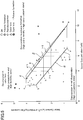
- the polarizing film laminate comprises a polarizing film comprised of a polyvinyl alcohol-based resin, and an optically transparent, polarizing film-protective film bonded to at least one of opposite surfaces of the polarizing film directly or through an additional optical film, wherein the polarizing film laminate contains an iodine concentration for the polarizing film and a water content for the polarizing film laminate which fall within a region surrounded, in an x-y orthogonal coordinate system in which the iodine concentration (wt.%) of the polarizing film is plotted on the x-axis, and the water content (g/m 2 ) of the polarizing film laminate is plotted on the y-axis, by: a first line segment connecting a first coordinate point at which the iodine concentration is 7.0
- the polarizing film laminate according to the first aspect can comprehensively solve the problems of "polyene formation”, “color loss” and “heat-caused red discoloration”.
- the polarizing film laminate according to the first aspect may have a film thickness of 4 to 20 ⁇ m.
- a polarizing film laminate used for an optical display panel configured to be mounted to a vehicle body of a powered vehicle.
- the polarizing film laminate comprises a polarizing film comprised of a polyvinyl alcohol-based resin, and an optically transparent, polarizing film-protective film bonded to at least one of opposite surfaces of the polarizing film directly or through an additional optical film, wherein the polarizing film laminate contains an iodine concentration for the polarizing film and a water content for the polarizing film laminate which fall within a region surrounded, in an x-y orthogonal coordinate system in which the iodine concentration (wt.%) of the polarizing film is plotted on the x-axis, and the water content (g/m 2 ) of the polarizing film laminate is plotted on the y-axis, by: a sixth line segment connecting a sixth coordinate point at which the iodine concentration is 4.5 wt% and the water content is 2.0
- the sixth coordinate point may be a coordinate point at which the iodine concentration is 4.0 wt% and the water content is 2.3 g/m 2
- the seventh coordinate point may be a coordinate point at which the iodine concentration is 4.0 wt% and the water content is 3.5 g/m 2 .
- the polarizing film laminate according to the second aspect may have a film thickness of 11 to 20 ⁇ m.
- a polarizing film laminate used for an optical display panel configured to be mounted to a vehicle body of a powered vehicle.
- the polarizing film laminate comprises a polarizing film comprised of a polyvinyl alcohol-based resin, and an optically transparent, polarizing film-protective film bonded to at least one of opposite surfaces of the polarizing film directly or through an additional optical film, wherein the polarizing film laminate contains an iodine concentration for the polarizing film and a water content for the polarizing film laminate which fall within a region surrounded, in an x-y orthogonal coordinate system in which the iodine concentration (wt.%) of the polarizing film is plotted on the x-axis, and the water content (g/m 2 ) of the polarizing film laminate is plotted on the y-axis, by: an eleventh line segment connecting a first coordinate point at which the iodine concentration is 7.0 wt% and the water content is is
- the polarizing film laminate according to the third aspect can comprehensively solve the problems of the "polyene formation", the "color loss” and the "heat-caused red discoloration".
- the eighth coordinate point may be a sixth coordinate point at which the iodine concentration is 4.5 wt% and the water content is 2.0 g/m 2
- the ninth coordinate point may be a tenth coordinate point at which the iodine concentration is 7.2 wt% and the water content is 2.0 g/m 2
- the polarizing film laminate according to the third aspect may have a film thickness of 4 to 11 ⁇ m.
- the polarizing film laminate preferably contains zinc.
- a single transmittance of the sample as measured after heating at 95°C for 500 hours is preferably equal or greater than that of the sample before the heating.
- an amount of change in cross transmittance of the sample at a wavelength of 410 nm due to heating at 95°C for 500 hours is preferably less than 1%, and an amount of change in cross transmittance of the sample at a wavelength of 700 nm due to the heating is preferably less than 5%.
- an amount of change in cross transmittance of the sample at a wavelength of 410 nm due to heating at 95°C for 500 hours is preferably 1% or more, and an amount of change in cross transmittance of the sample at a wavelength of 700 nm due to the heating is preferably less than 5%.
- an antireflective layer may be provided on a viewing-side surface of the polarizing film through a substrate, and wherein an antireflective film comprised of the substrate and the antireflective layer may have a water vapor permeability of equal to or more than 15 g/m 2 ⁇ 24 h.
- the polarizing film laminate according to any one of the first to third aspects comprises: a liquid crystal cell having a liquid crystal layer containing liquid crystal molecules oriented in one direction in a plane thereof in an electric field non-applied state; a first polarizing film disposed on one of opposite sides of the liquid crystal cell; a second polarizing film disposed on the other side of the liquid crystal cell, such that an absorption axis thereof becomes orthogonal to an absorption axis of the first polarizing film, wherein a first retardation layer and a second retardation layer are arranged between the first polarizing film and the liquid crystal cell, in this order from a side of the first polarizing film, wherein the first retardation layer is configured to satisfy a relationship of nxl > ny1 > nz1, where: nx1 represents a refractive index in an in-plane slow axis (x-axis) direction; ny1 represents a refractive index in an in-plane fast axis direction; and
- the polarizing film laminate according to any one of the first to third aspects comprises: a liquid crystal cell having a liquid crystal layer containing liquid crystal molecules oriented in one direction in a plane thereof in an electric field non-applied state; and a polarizing film disposed on one of opposite sides of the liquid crystal cell, wherein a retardation layer is disposed between the polarizing film and the liquid crystal cell, wherein the retardation layer is configured to satisfy a relationship of nx > nz > ny, where: nx represents a refractive index in an in-plane slow axis (x-axis) direction; ny represents a refractive index in an in-plane fast axis direction; and nz represents a refractive index in a thickness (z) direction.
- an optical display panel configured to be mounted to a vehicle body of a powered vehicle.
- the optical display panel comprises: an optical display cell; the polarizing film laminate according to any one of the first to third aspects, wherein the polarizing film laminate is bonded to one of opposite surfaces of the optical display cell directly or through an additional optical film; and an optically transparent cover plate disposed along the polarizing film laminate, on a side opposite to the optical display cell, and wherein any adjacent two of the optical display cell, the polarizing film laminate and the transparent cover plate are adhesively attach to each other by a transparent adhesive layer filled therebetween in a gap-free manner.
- the transparent cover plate may have a function of a capacitive touch sensor.
- an ITO layer serving as a component of the capacitive touch sensor may be provided between the transparent cover plate and the polarizing film laminate.
- the present invention makes it possible to comprehensively solve the problems of the "polyene formation", the "color loss” and the "heat-caused red discoloration”.
- the present invention is intended for an optical display panel, particularly an optical display panel configured to be mounted to a vehicle body of a powered vehicle such as an automobile, an electric train or an airplane, and a polarizing film laminate used for the optical display panel.
- a vehicle body is not necessarily limited to a case where the optical display panel or the polarizing film laminate is fixed to the vehicle body, but also includes a case where, when the optical display panel or the polarizing film laminate is used in, e.g., a smartphone or the like, it is freely brought in or carried in the powered vehicle.
- the term "mounted to a vehicle body” includes any situation where the optical display panel or the polarizing film laminate is used together with the powered vehicle, and is likely to be exposed to a high temperature or high humidity environment.
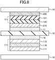
- FIG. 1 is a schematic diagram showing a layer configuration of an optical display panel 1.
- the optical display panel 1 comprises, at least, an optical display cell 10, a polarizing film laminate 12 laminated on one (viewing-side one) 10a of opposite surfaces of the optical display cell 10, and an optically transparent cover plate 14 disposed along the polarizing film laminate 12, on the side opposite to the optical display cell 10, i.e., on a viewing side.
- An additional polarizing film laminate 17 is disposed on the side of the other surface 10b of the optical display cell 10 through a transparent adhesive 16. Adjacent two of the optical display cell 10, the polarizing film laminate 12 and the cover plate 14 are adhesively attached to each other by a respective one of two transparent adhesives 11, 13 each filled therebetween in a gap-free manner.
- the term "adhesive" includes pressure-sensitive adhesive, unless otherwise specified.
- the optical display cell 10 may be adhesively attached to the polarizing film laminate 12 directly through the transparent adhesive 11. Alternatively, it may be adhesively attached to the polarizing film laminate 12 through an additional optical film such as a retardation film, or a viewing-angle compensation film (not illustrated), where needed.
- optical display cell 10 examples include a liquid crystal cell and an organic EL cell.
- a light emitter organic electroluminescence light emitter
- a transparent electrode an organic light-emitting layer and a metal electrode on a transparent substrate, in this order.
- the organic light-emitting layer is a laminate of various organic thin films, and it is possible to employ any of various layer configurations, such as: a laminate of a hole injection layer comprised of a triphenylamine derivative or the like and a light-emitting layer comprised of a fluorescent organic solid such as anthracene; a laminate of the light-emitting layer, and an electron injection layer comprised of a perylene derivative or the like; and a laminate of the hole injection layer, the light-emitting layer, and the electron injection layer.
- the liquid crystal cell it is allowable to use any one of a reflective liquid crystal cell using external light, a transmissive liquid crystal cell using light from a light source such as a backlight 18, and a transflective liquid crystal cell using both external light and light from a light source.
- the polarizing film laminate 17 is additionally disposed on the side opposite to the viewing side of the optical display cell (liquid crystal cell) 10, and a light source 18 such as a backlight is further disposed.
- the light source-side polarizing film laminate 17 and the liquid crystal cell 10 are adhesively attached to each other through a layer of the appropriate transparent adhesive 17.
- a driving mode of the liquid crystal cell it is possible to use any of various types such as VA mode, IPS mode, TN mode, STN mode, or bend alignment ( ⁇ ) mode.
- the cover plate 14 examples include a transparent plate (window layer) and a touch panel.
- a transparent plate a transparent plate having appropriate mechanical strength and thickness is used.
- a transparent resin plate such as an acrylic resin or a polycarbonate-based resin, or a glass plate.
- the surface of the cover plate 14 may be subjected to a low-reflection treatment, e.g., by using a low-reflection film (not illustrated).
- the touch panel any of various types of touch panels such as resistive film type, capacitance type, optical type and ultrasonic type, a glass or transparent resin plate having a touch sensor function or the like is used.
- a capacitance touch panel When a capacitance touch panel is used as the cover plate 14, it is preferable to provide a front transparent plate comprised of glass or a transparent resin plate, on the viewing side with respect to the touch panel.
- an ITO layer (not illustrated) serving as a component of the capacitance touch panel is provided in the transparent adhesive 13 bonding between the cover plate 14 and the polarizing film laminate 12.
- the transparent adhesives 11, 13, 16 it is possible to appropriately use any of various adhesives such as an adhesive as disclosed in JP 6071459B .
- a (meth)acrylic adhesive may be used, or a curable adhesive containing no (meth)acrylic acid may be used.
- an isoprene-based UV curable adhesive is preferably used.
- the isoprene-based UV curable adhesive may contain isoprene as a monomer component, or an isoprene derivative.
- the adhesive may contain a monomer component other than the isoprene-based monomer. Examples of the monomer component may include a (meth)acrylic acid derivative such as (meth)acrylic acid ester.
- reducing the content of an acid component in each of the transparent adhesives 11, 13, 16 is effective in suppressing a decrease in transmittance due to formation of polyene from polyvinyl alcohol.
- the polarizing film laminate 12 comprises, at least, a polarizing film 120, and a polarizing film-protective film 121 bonded to at least one (e.g., a viewing-side one) of opposite surfaces of the polarizing film 12.
- two polarizing film-protective films 121, 122 may be bonded, respectively, to the opposite surfaces of the polarizing film 120, i.e., a viewing-side one of the opposite surfaces of the polarizing film 120 and the other surface on the side opposite to the viewing-side surface, through an appropriate adhesive (not illustrated).
- an additional optical film may be provided between the polarizing film 120 and one or each of the polarizing film-protective films 121, 122.
- the present invention focuses on the concentration (wt. %) of iodine in the polarizing plate 120, and a water content (g/m 2 ) of the polarizing film laminate 12, in order to comprehensively solve problems occurring in a high temperature and high humidity environment, particularly the problem of the "polyene formation", the "color loss” and the "heat-caused red discoloration”.
- a value of each of these parameters can be adjusted during manufacturing of a respective one of the polarizing film and the polarizing film laminate.
- the polarizing film 120 is comprised of an iodine-containing polyvinyl alcohol (PVA)-based resin film.
- PVA polyvinyl alcohol
- PVA of a derivative thereof is used as a material for the PVA-based film used as the polarizing film.
- the derivative of PVA include polyvinyl formal and polyvinyl acetal, as well as polyvinyl alcohol modified with: olefin such as ethylene or propylene; an unsaturated carboxylic acid such as acrylic acid, methacrylic acid or crotonic acid; or an alkyl ester thereof; and an acryl amide.
- PVA a certain type of PVA having a polymerization degree of about 1000 to 10000, and a saponification degree of about 80 to 100 mol% is generally used.
- a PVA-based film made of this material tends to be more likely to contain water.
- the PVA-based film may contain an additive such as a plasticizer.
- a plasticizer include polyols and condensates thereof, such as glycerin, diglycerin, triglycerin, ethylene glycol, propylene glycol, and polyethylene glycol.
- the amount of the plasticizer to be used is preferably, but not limited to, 20 weight% or less, with respect to the total amount of the PVA-based film.
- the PVA-based film is subjected to dying in which it is dyed with iodine, and stretching in which it is stretched in at least one direction.
- a method is employed which is configured to subject the PVA-based film to a series of processes comprising swelling, dyeing, cross-linking, stretching, water washing and drying.
- the swelling process is performed, e.g., by immersing the PVA-based film in a swelling bath (water bath). Through this process, it is possible to wash off contamination or an antiblocking agent on the surface of the PVA-based film, and cause the PVA-based film to be swollen, thereby preventing non-uniformity such as dyeing unevenness.
- Glycerin, potassium iodide or the like may be appropriately added to the swelling bath.
- the temperature of the swelling bath is, e.g., about 20 to 60°C, and a time period of immersion in the swelling bath is, e.g., about 0.1 to 10 minutes.
- the dyeing process is performed, e.g., by immersing the PVA-based film in an iodine solution.
- the iodine solution is an iodine aqueous solution which contains iodine, and potassium iodide as dissolution aid.
- the concentration of iodine is, e.g., about 0.01 to 1 weight%, preferably 0.02 to 0.5 weight%.
- the concentration of potassium iodide is, e.g., about 0.01 to 10 weight%, preferably 0.02 to 8 weight%.
- the temperature of the iodine aqueous solution is, e.g., about 20 to 50°C, preferably 25 to 40°C.
- the immersion time period is, e.g., in the range of about 10 to 300 seconds, preferably 20 to 240 seconds.
- conditions such as the concentration of the iodine solution, the temperature and time period of immersion of the PVA-based film into the iodine aqueous solution, and others are adjusted such that each of the contents of iodine and potassium in the PVA-based film falls within a respective one of the above ranges.
- the cross-linking process is performed, i.e., by immersing the iodine-dyed PVA-based film in a process bath containing a cross-linking agent.
- a cross-linking agent any appropriate cross-linking agent may be employed.
- Specific examples of the cross-linking agent include boron compounds such as boric acid and borax, glyoxal, and glutaraldehyde. These may be used independently, or in combination.
- a solvent used for a solution of a cross-linking bath water is commonly used, wherein an organic solvent compatible with water may be added thereto in a proper amount.
- the cross-linking agent is used, e.g., in an amount of 1 to 10 weight parts, with respect to 100 weight parts of the solvent.
- the solution of the cross-linking bath preferably contains an aid such as an iodide.
- the concentration of the aid is preferably 0.05 to 15 weight%, more preferably 0.5 to 8 weight%.
- the temperature of the cross-linking bath is, e.g., about 20 to 70°C, preferably 40 to 60°C.
- a time period of immersion in the cross-linking bath is, e.g., about 1 second to about 15 minutes, preferably 5 seconds to 10 minutes.
- the stretching process is a process in which the PVA-based film is stretched in at least one direction.
- the PVA-based film is uniaxially stretched in a conveyance direction (longitudinal direction) thereof.
- a stretching method is not particularly limited, and any of a wet stretching method and a dry stretching method may be employed.
- the wet stretching method is employed, the PVA-based film is stretched in a process bath at a given ratio.
- a solution of a stretching bath it is preferable to use a solution obtained by adding a compound or the like necessary for various processes to a solvent such as water or an organic solvent (e.g., ethanol).
- the dry stretching method examples include an inter-roll stretching method, a heated roll stretching method, and a compression stretching method.
- the stretching process may be performed in any stage. Specifically, it may be performed simultaneously with the swelling, the dyeing or the cross-linking, or may be performed before or after any of these processes. Further, the stretching may be performed in a multi-stage manner.
- a cumulative stretch ratio of the PVA-based film is, e.g., 5 or more, preferably about 5 to 7.
- the PVA-based film subjected to the above processes is subjected to the water washing process and the drying process, according to the common procedure.
- the water washing process is performed, e.g., by immersing the PVA-based film in a water washing bath.
- the water washing bath may be pure water, or may be an aqueous solution of iodide (e.g., potassium iodide or sodium iodide).
- concentration of an iodide aqueous solution is preferably 0.1 to 10 weight %.
- An aid such as zinc sulfate or zinc chloride may be added to the iodide aqueous solution.
- the temperature of the water washing bath is, e.g., 5 to 50°C, preferably 10 to 45°C, more preferably 15 to 40°C.
- a time period of the immersion is, e.g., about 10 to 300 seconds, preferably 20 to 240 seconds.
- the water washing process may be implemented only once, or may be implemented plural times where needed. In a case where the water washing process is implemented plural times, the type and concentration of the additive contained in the water washing bath used for each process may be appropriately adjusted.
- the process of drying the PVA-based film is performed by any appropriate method (e.g., natural drying, blow drying, or drying by heating).
- a polarizing film having a film thickness of less than 6 ⁇ m can be manufactured by a manufacturing method disclosed in, e.g., JP 4751481B .
- This manufacturing method comprises: a laminate production process of forming a PVA-based resin film on a thermoplastic substrate; a stretching process of stretching the PVA-based resin film integrally with the thermoplastic substrate; and a dyeing process of adsorbing a dichroic material to the PVA resin layer.
- the PVA-based resin layer may be subjected to an insolubilization process, a cross-linking process, a drying process, a washing process, etc., where needed.
- the stretching process may be implemented before or after the dyeing process, and, in the stretching process, it is possible to employ either of in-air stretching, and in-water stretching such as stretching in a boric acid aqueous solution. Further, the stretching may be a single-stage stretching or may be two or more-stage or multi-stage stretching.
- the polarizing film is produced by stretching a PVA-based resin layer formed on a resin substrate, together with the resin substrate.
- a 200 ⁇ m-thick non-crystallizable ester-based thermoplastic resin substrate having a glass transition temperature of 75°C e.g., isophthalic acid-copolymerized polyethylene terephthalate copolymerized with 6 mol% of isophthalic acid (hereinafter referred to as "non-crystallizable PET") 6, and a PVA aqueous solution having a PVA concentration of 4 to 5 weight%, obtained by dissolving, in water, a PVA powder having a polymerization degree of 1000 or more and a saponification degree of 99% or more, are prepared.
- non-crystallizable PET isophthalic acid-copolymerized polyethylene terephthalate copolymerized with 6 mol% of isophthalic acid
- a laminate production apparatus 20 equipped with a coating device 21, a drying device 22 and a surface modifying unit 23
- the PVA aqueous solution is applied to the non-crystallizable PET substrate 6, and dried at a temperature of 50 to 60°C to form, on the PET substrate 1, a 7 ⁇ m-thick PVA layer 2 having a glass transition temperature of 80°C.
- a laminate 7 comprising the 7 ⁇ m-thick PVA layer is produced.
- the surface of the non-crystallizable PET substrate 6 can be subjected to corona treatment by the surface modifying unit 23, thereby improving adhesion between the non-crystallizable PET substrate 6 and the PVA layer 2 formed on the non-crystallizable PET substrate 6.
- the laminate 7 comprising the PVA layer will be produced as a 3 ⁇ m-thick polarizing film through the following processes including a 2-stage stretching process consisting of preliminary in-air stretching and in-boric-acid-solution stretching.
- a first-stage preliminary in-air stretching process (B), the laminate 7 comprising the 7 ⁇ m-thick PVA layer 2 is stretched integrally with the PET substrate 6 to form a "stretched laminate 8" comprising a 5 ⁇ m-thick PVA layer 2.
- the laminate 7 comprising the 7 ⁇ m-thick PVA layer 2 is subjected to free-end uniaxial stretching through the stretching device 31 of the oven 33 having a stretching temperature environment set at 130°C, so as to attain a stretch ratio of 1.8, thereby forming a stretched laminate 8.
- a roll 8' of the stretched laminate 8 can be produced by using a take-up unit 32 installed in side-by-side relation to the oven 33.
- a dyed laminate 9 is formed in which iodine as a dichroic material is adsorbed to the 5 ⁇ m-thick PVA layer 2 having oriented PVA molecules.
- the stretched laminate 8 unrolled from a feeding unit 43 installed in side-by-side relation to the dyeing apparatus 40 and loaded with the roll 8' is immersed in the dyeing solution 41 at a solution temperature of 30°C, for an arbitrary time, so as to allow a PVA layer constituting a finally-formed polarizing film to have a single transmittance of 40 to 44%, thereby forming a dyed laminate 9 in which iodine is absorbed to the molecularly-oriented PVA layer 2 of the stretched laminate 8.
- the dyeing solution 41 is prepared such that the concentration of iodine is set to 0.30 weight%, using water as a solvent. Further, in the dyeing solution 41, the concentration of potassium iodide for allowing iodine to be dissolved in water is set to 2.1 weight%. The concentration ratio of iodine to potassium iodide is 1 : 7.
- the stretched laminate 8 is immersed in the dyeing solution 41 having an iodine concentration of 0.30 weight% and a potassium iodide concentration of 2.1 weight%, for 60 seconds, thereby forming a dyed laminate 9 in which iodine is adsorbed to the 5 ⁇ m-thick PVA layer 2 having oriented PVA molecules.
- the dyed laminate 9 comprising the PVA layer 2 having molecularly-oriented iodine is further stretched to form an optical film laminate 60 which comprises the PVA layer having molecularly-oriented iodine and making up a 3 ⁇ m-thick polarizing film 3.
- the dyed laminate 9 continuously fed from the dyeing apparatus 40 is immersed in the boric acid aqueous solution 51 having a stretching temperature environment set at a solution temperature of 65°C, and then subjected to free-end uniaxial stretching through the stretching device 53 installed in the in-boric-acid-solution stretching apparatus 50, so as to attain a stretch ratio of 3.3, thereby forming an optical film laminate 60 comprising a 3 ⁇ m-thick PVA layer.
- the optical film laminate 60 comprising the polarizing film is preferably fed directly to a washing process (G).
- the washing process (G) is intended to wash off unnecessary residuals adhered on the surface of the polarizing film.
- the washing process (G) may be omitted, and the pulled-out optical film laminate 60 comprising the polarizing film may be directly fed to a drying process (H).
- the washed optical film laminate 60 is fed to the drying process (H) and dried therein. Then, the dried optical film laminate 60 is wound as a continuous web of the optical film laminate 60 by a take-up unit 91 installed in side-by-side relation to the drying apparatus 90, to form a roll of the optical film laminate 60 comprising the polarizing film.
- the drying process (H) it is possible to employ any appropriate method such as natural drying, blow drying and drying by heating.
- the drying may be performed by warm air at 60°C., for 240 seconds in an oven type drying apparatus 90.
- the polarizing film preferably contains zinc.
- the content of zinc in the polarizing film is preferably 0.002 to 2 weight%, more preferably 0.01 to 1 weight%.
- the polarizing film preferably contains sulfate ions.
- the content of sulfate ions in the polarizing film is preferably 0.02 to 0.45 weight%, more preferably 0.05 to 0.35 weight%, further preferably 0.1 to 0.25 weight%.
- the content of sulfate ions in the polarizing film is calculated from the content of sulfur atoms.
- the polarizing film manufacturing process it is preferable to perform a zinc impregnation process so as to allow zinc to be contained in the polarizing film. Further, in the polarizing film manufacturing process, it is preferable to perform sulfate ion process so as to allow sulfate ions to be contained in the polarizing film.
- the zinc impregnation process is performed, e.g., by immersing the PVA-based film in a zinc salt solution.
- a zinc salt solution an aqueous solution of an inorganic salt compound such as: zinc halide including zinc chloride and zinc iodide; zinc sulfate; or zinc acetate, is preferable.
- any of various zinc complex compounds may be used in the zinc impregnation process.
- an aqueous solution containing potassium ions and iodine ions derived from potassium iodide or the like is preferably used, because it can facilitate impregnation of zinc ions.
- the concentration of potassium iodide in the zinc salt solution is preferably 0.5 to 10 weight%, and more preferably 1 to 8 weight%.
- the sulfate ion process is performed, e.g., by immersing the PVA-based film in an aqueous solution containing a metal sulfate.
- a metal sulfate a certain type of metal sulfate is preferable which is more likely to be separated into sulfate ions and metal ions in a process liquid and then introduced into the PVA-based film in the form of ions.
- Examples of the type of metal forming the metal sulfate include: alkali metals such as sodium and potassium; alkaline earth metals such as magnesium and calcium; and transition metals such as cobalt, nickel, zinc, chromium, aluminum, copper, manganese, and iron.
- each of the zinc impregnation process and the sulfate ion process may be performed at any stage. That is, each of the zinc impregnation process and the sulfate ion process may be performed before or after the dyeing process.
- the zinc impregnation process and the sulfate ion process may be concurrently performed.
- the zinc impregnation process and the sulfate ion process are concurrently performed by using zinc sulfate as the zinc salt and the metal sulfate, and immersing the PVA-based film in a process bath containing zinc sulfate.
- the zinc impregnation process and/or the sulfate ion process can be performed concurrently with the dying process by allowing the zinc salt and/or the metal sulfate to coexist in the dying solution.
- Each of the zinc impregnation process and the sulfate ion process may be performed concurrently with the stretching.
- thermoplastic resin which is excellent in terms of transparency, mechanical strength and thermal stability.
- thermoplastic resin include: a cellulose-based resin such as triacetylcellulose; a polyester-based resin, polyether sulfone-based resin, a polysulfone-based resin, a polycarbonate-based resin, a polyamide-based resin, a polyimide-based resin, a polyolefin-based resin, a (meth)acrylic resin, a cyclic polyolefin-based resin (norbornene resin), a polyarylate-based resin, a polystyrene-based resin, a PVA-based resin, and mixtures thereof.
- the polarizing film-protective film may additionally have a function of a retardation film.
- the thickness of the polarizing film-protective film is appropriately adjusted to adjust the water content of the polarizing film laminate.
- the thickness is preferably about 1 to 500 ⁇ m, more preferably 2 to 300 ⁇ m, further preferably 5 to 200 ⁇ m.
- the polarizing film-protective film may contain one or more arbitrary types of additives.
- the additives include an ultraviolet absorber, an antioxidant, a lubricant, a plasticizer, a release agent, an anti-discoloration agent, a flame retardant, a nucleating agent, an antistatic agent, a pigment, and a colorant.
- the polarizing film and each of the polarizing film-protective films may be directly bonded together, they may be laminated together with an additional optical film.
- the additional (or other) optical film may include, but are not particularly limited to, a retardation film and a viewing-angle compensation film.
- the retardation film as the additional optical film may additionally have a function of a protective film.
- the polarizing film-protective film may additionally have a function of a retardation film, as mentioned above.
- the above retardation film as the additional optical film may be omitted.
- the above retardation film as the additional optical film may be provided.
- the polarizing film laminate substantially comprises two or three or more retardation films.
- a radical polymerization-curable adhesive for bonding between the polarizing film 120 and each of the polarizing film-protective films 121, 122 or bonding between the second film such as the retardation film and each of the films 120, 121, 122.
- the radical polymerization-curable adhesive comprises a radically polymerizable compound as a curable compound.
- the radically polymerizable compound may be a compound which is curable by active energy rays, or may be a compound which is curable by heat. Examples of the active energy rays include an electron beam, UV light, and visible light.
- the radically polymerizable compound examples include a compound containing a radically polymerizable functional group having a carbon-carbon double bond such as a (meth)acryloyl group or a vinyl group.
- a polyfunctional radically polymerizable compound is preferably used.
- the radically polymerizable compounds may be used independently or in the form of a combination of two or more of them. Further, the polyfunctional radically polymerizable compound and a monofunctional radically polymerizable compound may be used in combination.
- a compound having a high log P value (octanol/water partition coefficient) is preferably used, and it is also preferable to select a compound having a high log P value, as the radically polymerizable compound.
- the log P value is an index representing a lipophilic property of a material, and means a logarithmic value of the octanol/water partition coefficient.
- a higher log P value means stronger lipophilic property, i.e., lower water-absorbing property.
- the log P value can be measured (shake flask method described in JIS-Z-7260), and can be computed by calculation (ChemDraw Ultra manufactured by CambridgeSoft) based on structures of compounds each of which is a component (curable component or the like) of the curable adhesive.
- the log P value of the radically polymerizable compound is preferably 2 or more, more preferably 3 or more, particularly preferably 4 or more. As long as it falls within such a range, it is possible to prevent degradation of the polarizer due to water, and obtain a polarizing plate which is excellent in terms of durability under high temperature and high humidity.
- Examples of the polyfunctional radically polymerizable compound include: esterified products of a (meth)acrylate and a polyhydric alcohol, such as tripropylene glycol di(meth)acrylate, tetraethylene glycol di(meth)acrylate, 1,6-hexanediol di(meth)acrylate, 1,9-nonanediol di(meth)acrylate, 1,10-decanediol diacrylate, 2-ethyl-2-butylpropanediol di(meth)acrylate, bisphenol A di(meth)acrylate, bisphenol A-ethylene oxide adduct di(meth)acrylate, bisphenol A-propylene oxide adduct di(meth)acrylate, bisphenol A diglycidyl ether di(meth)acrylate, neopentyl glycol di(meth)acrylate, tricyclodecanedimethanol di(meth)acrylate, cyclic trimethylolpropane
- a polyfunctional radically polymerizable compound having a high log P value is preferable.
- the content rate of the polyfunctional radically polymerizable compound is preferably 20 to 97 weight%, more preferably 50 to 95 weight%, further preferably 75 to 92 weight%, particularly preferably 80 to 92 weight%, with respect to the total amount of the radically polymerizable compounds. As long as the content rate falls within such a range, it is possible to obtain a polarizing film which is excellent in terms of durability under high temperature and high humidity.
- Examples of the monofunctional radically polymerizable compound include a (meth)acrylamide derivative having a (meth)acrylamide group.
- a (meth)acrylamide derivative having a (meth)acrylamide group.
- the (meth)acrylamide derivative include: an N-alkyl group-containing (meth)acrylamide derivative such as N-methyl(meth)acrylamide, N,N-dimethyl(meth)acrylamide, N,N-diethyl(meth)acrylamide, N-isopropyl(meth)acrylamide, N-butyl(meth)acrylamide, or N-hexyl(meth)acrylamide; an N-hydroxyalkyl group-containing (meth)acrylamide derivative such as N-methylol(meth)acrylamide, N-hydroxyethyl(meth)acrylamide, or N-methylol-N-propane(meth)acrylamide; an N-aminoalkyl group-containing (meth)acrylamide derivative such as aminomethyl(meth) acrylamide or aminoethyl(meth)acrylamide; an N-alkoxy group-containing (meth)acrylamide derivative such as N-methoxymethylacrylamide or N-ethoxymethylacrylamide; and an N-
- heterocycle-containing (meth)acrylamide derivative in which an nitrogen atom of a (meth)acrylamide group forms a heterocycle
- it is possible to use e.g., N-acryloylmorpholine, N-acryloylpiperidine, N-methacryloylpiperidine, or N-acryloylpyrrolidine.
- N-hydroxyalkyl group-containing (meth)acrylamide derivative is preferable, and N-hydroxyethyl(meth)acrylamide is more preferable.
- the monofunctional radically polymerizable compound it is possible to use, e.g. a (meth)acrylic acid derivative having a (meth)acryloyloxy group; a carboxy group-containing monomer such as (meth)acrylic acid, carboxyethyl acrylate, carboxypentyl acrylate, itaconic acid, maleic acid, fumaric acid, crotonic acid, or isocrotonic acid; a lactam-based vinyl monomer such as N-vinylpyrrolidone, N-vinyl- ⁇ -caprolactam, or methylvinylpyrrolidone; and a vinyl-based monomer having a nitrogen-containing heterocycle, such as vinylpyridine, vinylpiperidone, vinylpyrimidine, vinylpiperazine, vinylpyrazine, vinylpyrrole, vinylimidazole, vinyloxazole, or vinylmorpholine.
- a (meth)acrylic acid derivative having a (meth)acryloyloxy group
- the content rate of the monofunctional radically polymerizable compound is preferably 3 to 80 weight%, more preferably 5 to 50 weight%, further preferably 8 to 25 weight%, particularly preferably 8 to 20 weight%, with respect to the total amount of the radically polymerizable compounds. As long as the content rate falls within such a range, it is possible to obtain a polarizing plate which is excellent in terms of durability under high temperature and high humidity.
- the radical polymerization-curable adhesive may further contain any other additive.
- the adhesive may further contain, e.g., a photopolymerization initiator, a photoacid generator, or a silane coupling agent.
- the adhesive may further contain, e.g., a thermal polymerization initiator or a silane coupling agent.
- additives examples include a polymerization inhibitor, a polymerization initiation aid, a leveling agent, a wettability improver, a surfactant, a plasticizer, a UV absorber, an inorganic filler, a pigment, and a dye.
- the cationic polymerization-curable adhesive contains a cationically polymerizable compound as the curable compound.
- the cationically polymerizable compound include a compound having an epoxy group and/or an oxetanyl group.
- the compound having an epoxy group it is preferable to use a compound having at least two epoxy groups in the molecule.
- the compound having an epoxy group include: a compound having at least two epoxy groups and at least one aromatic ring (aromatic epoxy compound); and a compound having at least two epoxy groups in the molecule, at least one of which is formed between two adjacent carbon atoms constituting an alicyclic ring (alicyclic epoxy compound).
- the cationic polymerization-curable adhesive preferably contains a photocationic polymerization initiator.
- the photocationic polymerization initiator is capable of generating a cationic species or a Lewis acid through irradiation with active energy rays such as visible light, UV light, X-rays, or an electron beam, thereby initiating a polymerization reaction of an epoxy group or an oxetanyl group.
- the cationic polymerization-curable adhesive may further contain the aforementioned additive.
- an aqueous solution e.g., solid content concentration: 0.5 to 60 weight% of an aqueous adhesive such as an isocyanate-based adhesive, a PVA-based adhesive, a gelatin-based adhesive, a vinyl-based latex, or an aqueous polyurethane is preferably used.
- the application of the adhesive may be performed with respect to one or both of any adjacent two of the polarizing film 120, the polarizing film-protective films 121, 122, and the additional optical film.
- a method is preferable which comprises immersing the polarizing film in an adhesive aqueous solution, and then laminating it to the polarizing film-protective films 121, 122 by using a roll laminator or the like.
- the thickness of the adhesive is, but not particularly limited to, about 30 to 100 nm as measured after drying.
- the polarizing film-protective films and the additional optical film are laminated together through the adhesive, the resulting laminate is subjected to the drying process.
- This laminate drying process is performed for the purpose of drying and solidifying the adhesive, and additionally reducing the water content for improving initial optical properties of the polarizing film laminate.
- a drying method drying by heating is commonly used.
- a drying condition a drying temperature is preferably set in the range 50 to 95°C, more preferably in the range 60 to 85°C.
- the drying condition of the laminate is not particularly limited. However, in view of the efficiency and practicality of the drying, the drying temperature is preferably 50°C or more. Further, from a viewpoint of uniforming optical properties of the polarizing film laminate, it is preferably 95°C or less. The drying may be implemented while the drying temperature is raised stepwisely within the above temperature range.
- the drying of the laminate may be performed successively with respect to the bonding of the polarizing film, the polarizing film-protective films and the additional optical film.
- the drying may be performed as a separate process.
- the high-temperature and long-time drying is preferable from the viewpoint of reducing the water content of the polarizing film laminate, and is, on the other hand, likely to lead to deterioration in optical properties or the like of the polarizing film laminate.
- a polarizing film-protective film having a small saturated water absorption, or a polarizing film-protective film having a high water vapor permeability it becomes possible to adjust the water content of the polarizing film laminate in the aforementioned desired range, without employing harsh drying conditions.
- the single transmittance of the polarizing film laminate decreases. This decrease is presumed to be caused by formation of polyene from PVA.
- the polyene causes a significant decrease in transmittance of the polarizing film.
- a PVA-polyiodine complex is more likely to be disassembled, thereby forming I - or I 2 .
- the polyene formation is considered to occur as a result of a situation where a dehydration reaction is promoted by iodine (I 2 ) formed in the high temperature and high humidity environment and heating, as shown in the following chemical formula 1.
- I 2 arising as a result of a situation where a PVA-polyiodine complex existing in the polarizing film is disassembled by heating, and an OH group form a charge-transfer complex (HO - - - I 2 ), and then the charge-transfer complex is formed as polyene through an OI group.
- iodine-dyed and stretched PVA-based film polarizing film
- iodine forms a complex in cooperation with molecularly oriented PVA, in the form of polyiodine ions of I 3 - and I 5 - (PVA-polyiodine complex).
- cross-linking points are formed in PVA by a cross-linking agent such as boric acid, thereby maintaining an orientation property of the PVA.
- the orientation property of the PVA is deteriorated, causing disassembly of the PVA-polyiodine complex.
- the color loss occurs in a black display state.
- iodine forms a complex in cooperation with PVA, in the form of polyiodine ions of I 3 - and I 5 - (PVA-polyiodine complex).
- I 3 - has an absorption peak around 470 nm
- I 5 - has an absorption peak around 600 nm. That is, a PVA-I 3 - complex undertakes a roll of absorbing the short wavelength-side (blue-side) light, and a PVA-I 5 - complex undertakes a roll of absorbing the long wavelength-side (red-side) light.
- the PVA-I 5 - complex is weak against heating.
- the PVA-I 5 - complex is disassembled, and I 5 - is broken.
- the PVA-I 5 - complex undertaking the roll of absorbing the long wavelength-side light decreases, i.e. the transmittance on the long wave side with respect to about 700 nm rises, so that the polarizing film is discolored to red.
- samples of various polarizing film laminates which are different from each other in terms of "the film thickness ( ⁇ m) of a polarizing film", and/or “the iodine concentration (wt.%) of the polarizing film", and/or “the water content (g/m 2 ) of a polarizing film laminate” were prepared.
- the film thickness ( ⁇ m) of a polarizing film is measured using a spectroscopic film thickness meter MCPD-1000 (manufactured by Otsuka Electronics Co., Ltd.). The thickness of a polarizing film-protective film is also measured using this meter.
- the polarizing film comprised in each sample can be taken out by immersing the sample in a solvent to dissolve polarizing film-protective films in the solvent.
- the solvent it is possible to use dichloromethane, cyclohexane, and methyl ethyl ketone when each of the polarizing film-protective films is formed of a triacetylcellulose resin, a cycloolefin resin, and an acrylic resin, respectively.
- these resins may be sequentially dissolved using two of the above solvents.
- the iodine concentration (wt.%) of the polarizing film can be changed, e.g., by adjusting the concentration of an iodine aqueous solution in which a PVA-based film or PVA layer is to be immersed, and/or a time period of the immersion, during manufacturing of the polarizing plate.
- the iodine concentration of the polarizing film is measured in the following manner.
- the polarizing film comprised in each sample can be taken out by immersing the sample in a solvent to dissolve the polarizing film-protective films in the solvent, in the same manner as that in the measurement of the film thickness of the polarizing film.
- the iodine concentration is quantitatively determined using a calibration curve method for fluorescent X-ray analysis.
- a fluorescent X-ray analyzer ZSX-PRIMUS IV manufactured by Rigaku Corporation
- a value to be directly obtained by the fluorescent X-ray analyzer is not the concentration of each element, but a fluorescent X-ray intensity (kcps) at a wavelength unique to each element.
- kcps fluorescent X-ray intensity
- iodine concentration of a polarizing film here means an iodine concentration (wt.%) on the basis of the weight of the polarizing film.
- the calibration curve is created in the following steps. 1. A known amount of potassium iodide is dissolved in a PVA aqueous solution to produce 7 types of PVA aqueous solutions each containing iodine in a known concentration. Each of the PVA aqueous solutions is applied onto polyethylene terephthalate, and, after drying, peeled off, to produce samples 1 to 7 of PVA films each containing iodine in a known concentration.
- the iodine concentration (wt.%) of each PVA film is calculated by the following mathematical formula 1. Iodine concentration wt .
- the fluorescent X-ray intensity (kcps) corresponding to iodine is measured using the fluorescent X-ray analyzer ZSX-PRIMUS IV (manufactured by Rigaku Corporation).
- the fluorescent X-ray intensity (kcps) is defined as a peak value of a fluorescent X-ray spectrum.
- the film thickness of each of the produced PVC films is measured using the spectroscopic film thickness meter MCPD-1000 (manufactured by Otsuka Electronics Co., Ltd.). 3.
- the fluorescent X-ray intensity is divided by the film thickness of the PVC film to obtain a fluorescent X-ray intensity per unit thickness of the film (kcps/ ⁇ m).
- the iodine concentration and the per-unit thickness fluorescent X-ray intensity are shown in the following Table 1.
- a mathematical formula for determining the iodine concentration from the fluorescent X-ray intensity per unit thickness of the PVA film is set as the following mathematical formula 2.
- R2 denotes a correlation coefficient.
- Iodine concentration wt % 14.474 ⁇ Fluorescent X-ray intensity per unit thickness of PVA film kcps / ⁇ m
- the fluorescent X-ray intensity obtained by the measurement of each sample is divided by the thickness to determine the per-unit thickness fluorescent X-ray intensity (kcps/ ⁇ m).
- the per-unit thickness fluorescent X-ray intensity of each sample is assigned to the mathematical formula 2 to determine the iodine concentration.
- the water content (g/m 2 ) of the polarizing film laminate can be determined by mainly adjusting the film thickness of the polarizing film, and the material, thickness, etc., of the polarizing film-protective film to be bonded to the polarizing film. It can also be adjusted by the cross-linking process (the content of boracic acid, etc.) during manufacturing of the polarizing film.
- the water content of the polarizing film laminate is measured in the following manner.
- the polarizing film laminate obtained in each of Inventive and Comparative Examples is cut into a square piece having a size of 0.1 m ⁇ 0.1 m.
- the cut sample is put in a thermo-hygrostat, and left in an environment having a temperature of 23°C and a relative humidity of 55% for 48 hours. Subsequently, in a clean room set in the same environment of the thermo-hygrostat, i.e., at a temperature of 23°C and a relative humidity of 55%, the sample is extracted from the thermo-hygrostat, and the weight of the sample is measured within 5 minutes after the extraction. The weight of the sample at that time is defined as an initial weight W1 (g).
- the extracted sample is put in a dry oven, and dried at 120°C for 2 hours. Subsequently, in the above clean room set at a temperature of 23°C and a relative humidity of 55%, the dried sample is extracted from the dry oven, and the weight of the sample is measured within 10 minutes after the extraction.
- the weight of the sample at that time is defined as a post-drying weight W2 (g).
- W2 post-drying weight
- the elapsed time period is set to within 10 minutes, instead of within 5 munities, because a cooling time period is taken into account. In this case, as with the above, as long as the elapsed time period after the extraction falls within about 15 minutes, the fluctuations do not exert any substantial influence on the post-drying weight,
- an equilibrium water content M (g/m 2 ) is calculated by the following formula using the initial weight W1 and the post-drying weight W2 of the sample obtained in the above manner.
- M W 1 ⁇ W 2 / 0.1 ⁇ 0.1
- water content of the polarizing film laminate here means the equilibrium water content calculated in the above manner.
- One surface of the resin substrate was subjected to corona treatment (treatment condition: 55 W ⁇ min/m 2 ), and an aqueous solution obtained by adding potassium iodide to PVA containing a combination of 90 weight parts of PVA (polymerization degree: 4,200, saponification degree: 99.2 mol %) and 10 weight parts of acetoacetyl-modified PVA (trade name "GOHSEFIMER Z410", manufactured by the Nippon Synthetic Chemical Industry Co., Ltd.), in an amount of 13 weight parts with respect to the amount of the PVA, was applied to the corona-treated surface at normal temperature. Subsequently, the applied solution was dried at 60°C to form a 13 ⁇ m-thick PVA-based resin layer, thereby producing a laminate.
- corona treatment treatment condition: 55 W ⁇ min/m 2
- the obtained laminate was subjected to free-end uniaxial stretching, in such a manner as to be stretched in a longitudinal direction (lengthwise direction) thereof, between rolls having different peripheral speeds in an oven at 130°C, to attain a stretch ratio of 2.0 (in-air auxiliary stretching process).
- the laminate was immersed in an insolubilization bath (a boric acid aqueous solution obtained by adding 4 weight parts of boric acid to 100 weight parts of water) having a solution temperature of 40°C for 30 seconds (insolubilization process).
- an insolubilization bath a boric acid aqueous solution obtained by adding 4 weight parts of boric acid to 100 weight parts of water having a solution temperature of 40°C for 30 seconds (insolubilization process).
- the laminate was immersed in a dyeing bath (an iodine aqueous solution obtained by adding iodine and potassium iodide mixed at a weight ratio of 1 : 7 to 100 weight parts of water) having a solution temperature of 30°C, for 60 seconds, while the concentrations of them were adjusted to attain a designated transmittance, (dyeing process).
- a dyeing bath an iodine aqueous solution obtained by adding iodine and potassium iodide mixed at a weight ratio of 1 : 7 to 100 weight parts of water having a solution temperature of 30°C, for 60 seconds, while the concentrations of them were adjusted to attain a designated transmittance, (dyeing process).
- the laminate was immersed in a cross-linking bath (a boric acid aqueous solution obtained by adding 3 weight parts of potassium iodide and 3 weight parts of boric acid to 100 weight parts of water) having a solution temperature of 40°C for 30 seconds (cross-linking process).
- a cross-linking bath a boric acid aqueous solution obtained by adding 3 weight parts of potassium iodide and 3 weight parts of boric acid to 100 weight parts of water having a solution temperature of 40°C for 30 seconds (cross-linking process).
- the laminate was immersed in a boric acid aqueous solution (boric acid concentration: 3.0 weight%) having a solution temperature of 70°C, the laminate was subjected to uniaxial stretching, in such a manner as to be stretched in the longitudinal direction (lengthwise direction) between rolls having different peripheral speeds, to attain a total stretch ratio of 5.5 (in-boric-acid-solution stretching process).
- boric acid aqueous solution boric acid concentration: 3.0 weight%) having a solution temperature of 70°C
- the laminate was immersed in a washing bath (an aqueous solution obtained by adding 4 weight parts of potassium iodide to 100 weight parts of water) having a solution temperature of 20°C (washing process).
- a washing bath an aqueous solution obtained by adding 4 weight parts of potassium iodide to 100 weight parts of water having a solution temperature of 20°C (washing process).
- the laminate was brought into contact with a metal roll made of SUS and having a surface temperature kept at 75°C for 2 seconds or more (heated roll drying process).
- a cycloolefin-based film (ZT12, manufactured by Zeon Corporation, 18 ⁇ m) was bonded, as the polarizing film-protective film, to a surface of the obtained polarizing film on the side opposite to the resin substrate, through an ultraviolet curable adhesive.
- the after-mentioned curable adhesive was applied to allow a final thickness to become 1.0 ⁇ m, and the cycloolefin-based film is bonded using a roll machine.
- UV light was emitted from the side of the cycloolefin-based film to cure the adhesive.
- the resin substrate was peeled off to obtain a polarizing film laminate comprising the cycloolefin-based polarizing film-protective film and the polarizing film.
- the details of the curable adhesive are as follows. 40 weight parts of N-hydroxyethyl acrylamide (HEAA), 60 weight parts of acryloyl morpholine (ACMO) and 3 weight parts of a photoinitiator "IRGACURE 819" (manufactured by BASF SE) were mixed to prepare an adhesive. This adhesive was applied onto the polarizing film to allow the thickness of an adhesive layer after curing to become 1.0 ⁇ m, and irradiated and cured with ultraviolet light as active energy energy rays. The ultraviolet irradiation was performed using a gallium-sealed metal halide lamp, an irradiation device: Light HAMMER 10, manufactured by Fusion UV Systems, Inc.
- the polarizing film was extracted from the polarizing film-protective film by using cyclohexane as a solvent, and the iodine concentration of the extracted polarizing plate was measured.
- the concentration of the iodine aqueous solution and the immersion time period in the dyeing process were adjusted to change the iodine concentration. Further, the thickness of the polarizing film-protective film was adjusted to change the water content of the polarizing film laminate. The remaining conditions were the same as those in Inventive Example 1.
- the concentration of the iodine aqueous solution and the immersion time period in the dyeing process were adjusted to change the iodine concentration. Further, the thickness of the polarizing film-protective film was adjusted to change the water content of the polarizing film laminate. Further, in the production of the polarizing film laminate in Inventive Example 1, a cycloolefin-based film (ZF12, manufactured by Zeon Corporation, 13 ⁇ m) was bonded, as the polarizing film-protective film. The remaining conditions were the same as those in Inventive Example 1.
- a triacetyl cellulose film-based film (TJ40UL, manufactured by FUJIFILM Corporation, thickness: 40 ⁇ m) was bonded, as the polarizing film-protective film. Further, in the production of the polarizing film in Inventive Example 1, the concentration of the iodine aqueous solution and the immersion time period in the dyeing process were adjusted to change the iodine concentration. The remaining conditions were the same as those in Inventive Example 1.
- a 40 ⁇ m-thick transparent protective film (manufactured by Nitto Denko Corporation) comprised of a modified acrylic polymer having a lactone ring structure was bonded, as the polarizing film-protective film. Further, in the production of the polarizing film in Inventive Example 1, the concentration of the iodine aqueous solution and the immersion time period in the dyeing process were adjusted to change the iodine concentration. The remaining conditions were the same as those in Inventive Example 1.
- a 30 ⁇ m-thick PVA film having an average polymerization degree of 2,700 was conveyed while being dyed and stretched between rolls having different peripheral speed ratios. Firstly, the PVA film was stretched in a conveyance direction thereof to attain a stretch ratio of 1.2, while being immersed and swelled in a water bath at 30°C for 1 minute, and then stretched in the conveyance direction to attain a stretch ratio of 3 (on the basis of an unstretched state of the PVA film), while being immersed in and dyed by an aqueous solution (solution temperature: 30°C) of potassium iodide (0.03 weight%) and iodine (0.3 weight%) for 1 minute.
- the stretched film was stretched in the conveyance direction to attain a stretch ratio of 6 (on the basis of the unstretched state of the PVA film), while being immersed in an aqueous solution (bath solution) of boric acid (4 weight%), potassium iodide (5 weight%) and zinc sulfate (3.5 weight%) for 30 seconds. After the stretching, the stretched film was dried in an oven at 40°C for 3 minutes to obtain a 12 ⁇ m-thick polarizing film.
- an aqueous solution containing an acetoacetyl group-containing polyvinyl alcohol resin (average polymerization degree: 1200, saponification degree: 98.5 mol%, acetoacetylation degree: 5 mol%), and methylol melamine at a weight ratio of 3 : 1 was used.
- a 20 ⁇ m-thick transparent protective film (manufactured by Nitto Denko Corporation) comprised of a modified acrylic polymer having a lactone ring structure, and a 27 ⁇ m-thick transparent protective film obtained by forming a 2 ⁇ m-thick hard coat layer (HC) on a 25 ⁇ m-thick triacetyl cellulose film (trade name "KC2UA", manufactured by Konica Minolta, Inc.) were bonded, respectively, to one of opposite surfaces and the other surface of the polarizing film by using a roll laminator. Subsequently, the resulting laminate was heated and dried in an oven at 70°C for 5 minutes to obtain a polarizing film laminate having the transparent protective films bonded, respectively, to the opposite surfaces thereof.
- HC 2 ⁇ m-thick hard coat layer
- KC2UA triacetyl cellulose film
- the hard coat layer was formed in the following manner. Firstly, a hard coat layer-forming material was prepared. This hard coat layer-forming material was produced by adding, to a resin solution (trade name "UNIDIC 17-806", manufactured by DIC Corporation, solid content concentration: 80%) obtained by dissolving a UV-curable resin monomer or oligomer consisting mainly of urethane acrylate, in butyl acetate, 5 weight parts of a photopolymerization initiator (product name "IRGACURE 906", manufactured by BASF SE) and 0.01 weight part of a leveling agent (product name "GRANDIC PC4100", manufactured by DIC Corporation) per 100 weight parts of a solid content in the solution, and then adding, to the resulting mixed solution, cyclopentanone (hereinafter expressed to as "CPN”) and propylene glycol monomethyl ether (hereinafter expressed as "PGM”) at a ratio of 45:55 to allow the solid content concentration in the solution to become 36 weight%.
- a resin solution trade
- the hard coat layer-forming material produced in the above manner was applied onto a transparent protective film to allow the thickness of a hard coat after curing to become 2 ⁇ m, thereby forming a coating film. Then, the coating film was dried at 90°C for 1 minute, and then subjected to curing process by means of irradiation with ultraviolet light from a high-pressure mercury lamp in a cumulative dose of 300 mJ/cm 2 .
- the polarizing film was extracted from the polarizing film-protective film by using dichloromethane and methyl ethyl ketone as a solvent, and the iodine concentration of the extracted polarizing plate was measured.
- the concentration of the iodine aqueous solution and the immersion time period in the dyeing process were adjusted to change the iodine concentration.
- a 30 ⁇ m-thick transparent protective film (manufactured by Nitto Denko Corporation) comprised of a modified acrylic polymer having a lactone ring structure, and a 49 ⁇ m-thick transparent protective film obtained by forming a 9 ⁇ m-thick HC on a 40 ⁇ m-thick triacetyl cellulose film (trade name "KC4UY", manufactured by Konica Minolta, Inc.) were bonded, respectively, to one surface and the other surface of the obtained polarizing film.
- the remaining conditions were the same as those in Inventive Example 6.
- a 30 ⁇ m-thick transparent protective film (manufactured by Nitto Denko Corporation) comprised of a modified acrylic polymer having a lactone ring structure, and a triacetyl cellulose film-based film ("TJ40UL", manufactured by FUJIFILM Corporation, thickness: 40 ⁇ m) were bonded, respectively, to one surface and the other surface of the obtained polarizing film.
- TJ40UL triacetyl cellulose film-based film
- the concentration of the iodine aqueous solution and the immersion time period in the dyeing process were adjusted to change the iodine concentration. Further, the thickness of the polarizing film-protective film was adjusted to change the water content of the polarizing film laminate. The remaining conditions were the same as those in Inventive Example 8.
- the concentration of the iodine aqueous solution and the immersion time period in the dyeing process were adjusted to change the iodine concentration. Further, the thickness of the polarizing film-protective film was adjusted to change the water content of the polarizing film laminate. The remaining conditions were the same as those in Inventive Example 1.
- a cycloolefin-based film (ZD12, manufactured by Zeon Corporation, 27 ⁇ m) was bonded, as the polarizing film-protective film. Further, the concentration of the iodine aqueous solution and the immersion time period in the dyeing process were adjusted to change the iodine concentration, and the thickness of the polarizing film-protective film was adjusted to change the water content of the polarizing film laminate. The remaining conditions were the same as those in Inventive Example 1.
- the concentration of the iodine aqueous solution and the immersion time period in the dyeing process were adjusted to change the iodine concentration. Further, the thickness of the polarizing film-protective film was adjusted to change the water content of the polarizing film laminate. The remaining conditions were the same as those in Comparative Example 3.
- a laminate formed with a 10 ⁇ m-thick PVA-based resin layer was subjected to, e.g., the in-air auxiliary stretching and the in-boric-acid-solution stretching, to obtain a 4.0 ⁇ m-thick polarizing film.
- a cycloolefin-based film ZD12, manufactured by Zeon Corporation, 27 ⁇ m was bonded, as the polarizing film-protective film.
- the concentration of the iodine aqueous solution and the immersion time period in the dyeing process were adjusted to change the iodine concentration, and the thickness of the polarizing film-protective film was adjusted to change the water content of the polarizing film laminate.
- the remaining conditions were the same as those in Inventive Example 1.
- the concentration of the iodine aqueous solution and the immersion time period in the dyeing process were adjusted to change the iodine concentration. Further, the thickness of the polarizing film-protective film was adjusted to change the water content of the polarizing film laminate. The remaining conditions were the same as those in Inventive Example 6.
- the concentration of the iodine aqueous solution and the immersion time period in the dyeing process were adjusted to change the iodine concentration. Further, the thickness of the polarizing film-protective film was adjusted to change the water content of the polarizing film laminate. The remaining conditions were the same as those in Inventive Example 7.
- the concentration of the iodine aqueous solution and the immersion time period in the dyeing process were adjusted to change the iodine concentration. Further, the thickness of the polarizing film-protective film was adjusted to change the water content of the polarizing film laminate. The remaining conditions were the same as those in Inventive Example 6.
- the concentration of the iodine aqueous solution and the immersion time period in the dyeing process were adjusted to change the iodine concentration. Further, the thickness of the polarizing film-protective film was adjusted to change the water content of the polarizing film laminate. The remaining conditions were the same as those in Inventive Examples 8 to 14.
- polarizing films in Inventive Examples 8 to 14 a 60 ⁇ m-thick PVA film was conveyed and stretched in the stretching process to obtain a 22.0 ⁇ m-thick polarizing film. Further, the concentration of the iodine aqueous solution and the immersion time period in the dyeing process were adjusted to change the iodine concentration, and the thickness of the polarizing film-protective film was adjusted to change the water content of the polarizing film laminate. The remaining conditions were the same as those in Inventive Examples 8 to 14.
- polarizing film-protective films As the polarizing film-protective films, a 30 ⁇ m-thick transparent protective film (manufactured by Nitto Denko Corporation) comprised of a modified acrylic polymer having a lactone ring structure, and a 49 ⁇ m-thick transparent protective film obtained by forming a 9 ⁇ m-thick HC on a 40 ⁇ m-thick triacetyl cellulose film (trade name "KC4UY", manufactured by Konica Minolta, Inc.) were bonded, respectively, to one surface and the other surface of the obtained polarizing film. The remaining processes were the same as those in Inventive Examples 8 to 14.
- the concentration of the iodine aqueous solution and the immersion time period in the dyeing process were adjusted to change the iodine concentration. Further, the thickness of the polarizing film-protective film was adjusted to change the water content of the polarizing film laminate. Further, a 20 ⁇ m-thick transparent protective film (manufactured by Nitto Denko Corporation) comprised of a modified acrylic polymer having a lactone ring structure was bonded, as the polarizing film-protective film, to one surface of the polarizing film. The remaining conditions were the same as those in Comparative Example 13.
- CS9868US manufactured by Nitto Denko Corporation having a thickness of 200 ⁇ m was used for one surface of the polarizing film laminate
- an acrylic pressure-sensitive adhesive (thickness: 20 ⁇ m) used for a polarizing film laminate CRT1794YCU (manufactured by Nitto Denko Corporation) was used for the other surface of the polarizing film laminate.
- the acrylic pressure-sensitive adhesive used for the other surface was obtained in the following manner.
- the single transmittance of each sample was measured before and after the 95°C/500 H heating test, and the amount of change ⁇ Ts in the single transmittance was determined by the following formula: ⁇ Ts + ⁇ Ts 500 ⁇ Ts 0 where Tso indicates the single transmittance of the sample which was measured before heating, while ⁇ T S500 indicates the single transmittance thereof which was measured after 95°C/500 H heating.
- the sample When the change amount ⁇ Ts has a negative value, the sample was evaluated as "polyene formation (decrease in the single transmittance)". In other words, when the single transmittance after heating of 95°C/500 H is equal to or greater than the single transmittance before the heating, the sample was evaluated as having no problem regarding the polyene formation.
- the single transmittance was measured using a spectrophotometer (product name "DOT-3", manufactured by Murakami Color Research Laboratory Co., Ltd.).
- DOT-3 manufactured by Murakami Color Research Laboratory Co., Ltd.
- the single transmittance can be determined according to JIS Z 8701.
- crossed transmittances (%) at a wavelength of 410 nm and a wavelength of 700 nm were measured before and after the 95°C/250 H heating test by the aforementioned spectrophotometer, to determine the change amounts ⁇ T S410 and ⁇ T S700 at the respective wavelengths.
- the sample was evaluated as having no problem regarding the color loss.
- the sample when the amount of change in the crossed transmittance at a wavelength of 410 nm due to the 95°C/500 H heating test is equal to or greater than 1% and the amount of change in the crossed transmittance at a wavelength of 700 nm due to the 95°C/500 H heating test is less than 5%, the sample was evaluated as having no problem regarding the heat-caused red discoloration.
- FIG. 5 is a graph in which results of Inventive and Comparative Examples are plotted on an x-y orthogonal coordinate system.
- the x-axis (horizontal axis) represents the iodine concentration (weight%) of the polarizing film, and the y-axis represents the water content (g/m 2 ) of the polarizing film laminate.
- FIG. 6 One example of a layer configuration in which the antireflective function is added to the polarizing film laminate 12 is shown in FIG. 6 in the form of a schematic diagram.
- a layer element corresponding to the already-mentioned layer element will be assigned with the same reference sign as that of the already-mentioned layer element.
- the antireflective function can be added by providing an antireflective film 200 on the viewing side of the polarizing film laminate 12 through a pressure-sensitive adhesive 13.
- the antireflective film 200 comprises a transparent substrate 201 and an antireflective layer 202 disposed on the transparent substrate 201.
- the transparent substrate 201 may be configured to additionally serve as a polarizing film protective film (e.g., the polarizing film-protective film 121 in the configuration in FIG. 1 ) constituting the optical film laminate 12.
- an optical film thickness (product of the refractive index and the thickness) of a thin film is adjusted such that inverted phases of incident light and reflected light cancel each other out.
- a material for the thin film constituting the antireflective layer 202 include an oxide, nitride, and fluoride of a metal.
- examples of a low refractive index material having a refractive index of 1.6 or less at a wavelength of 550 nm include a silicon oxide and a magnesium fluoride.
- Examples of a high refractive index material having a refractive index of 1.9 or more at a wavelength of 550 nm include a titanium oxide, a niobium oxide, a zirconium oxide, a tin-doped indium oxide (ITO), and an antimony-doped tin oxide (ATO).
- the antireflective layer 202 may a single layer, it is preferably an alternative laminate of a low refractive index layer and a high refractive index layer.
- a thin film to be provided as the outermost surface layer of the antireflective layer 202 is preferably a low refractive index layer.
- Materials for the low refractive index layer and the high refractive index layer are preferably oxides as mentioned above.
- the antireflective layer 202 is preferably an alternative laminate of a silicon oxide (Si02) thin film as a low refractive index layer and a niobium oxide (Nb 2 O 5 ) thin film as a high refractive index layer.
- a method of forming the thin film constituting the antireflective layer 202 may be, but not particularly limited to, a wet coating method or a dry coating method. From a view point of being capable of forming a dense thin film having an even film thickness, the dry coating method such as vacuum deposition, CVD, sputtering, electron beam deposition are preferable. Sputtering among others is particularly preferable, because of its capability of forming a film having high mechanical strength.
- Productivity of the antireflective film can be increased by continuously forming films with conveying elongate film substrates in one direction (longitudinal direction thereof) by a roll-to-roll process.
- a deposition material is sputtered from a target by bringing a high-energy sputtering gas (e.g., Ar) into collision with the target, and thus sputtered particles also have high energy. Therefore, in sputtering, a dense film is more likely to be formed, as compared with vacuum deposition or CVD Generally, a thin film formed by sputtering has a low water vapor permeability, e.g., the water vapor permeability of a silicon oxide film is equal to or less than 10 g/m 2 ⁇ 24 h, in many cases.
- a high-energy sputtering gas e.g., Ar
- a thin film having a water vapor permeability of equal to or less than 15 g/m 2 24 h can be formed by adjusting conditions for sputtering film formation. For example, when a discharge voltage during sputtering film formation is relatively low, kinetic energy of sputtered particles is reduced, so that diffusion at the surface of a substrate is suppressed. Thus, the film is apt to grow in a columnar shape, so that it is likely to become porous. When the discharge voltage is relatively high, the film is apt to be formed in a planar shape, so that it is likely to become dense. On the other hand, when the discharge voltage is excessively increased, neutral particles such as recoil Ar damages the surface of the film to cause defects therein, so that the density of the film tends to be lowered.
- the magnetic flux density of the surface of the target surface during sputtering film formation is preferably 20 mT or more, more preferably 35 mT or more, further preferably 45 mT or more, particularly preferably 55 mT or more.
- the film formation pressure is preferably 0.4 Pa to 1.5 Pa.
- the surface profile or the like of the substrate serving as a base for film formation can also exert an influence on a film growth mode.
- a sputtered film is more likely to grow in a columnar shape, due to irregularities formed at the surface, so that the water vapor permeability tends to become larger.
- the polarizing film laminate 12 provided with the antireflective layer 202 In a situation where the polarizing film laminate 12 provided with the antireflective layer 202 is exposed to a heating environment, water in the polarizing film 120 and the polarizing film-protective films 121, 122 will be vaporized and released to the outside.
- the water vapor permeability of the antireflective layer 202 is relatively small, the water is less likely to be diffused to the outside.
- the transparent substrate 201 comprised of triacetyl cellulose is likely to be hydrolyzed, and protective performance for the polarizing film 120 tends to be deteriorated.
- the acetyl cellulose is hydrolyzed, a free acid is generated.
- the problems of the polyene formation and others are suppressed by adjusting the iodide concentration of the polarizing film and the water content of the polarizing film laminate.
- the water vapor permeability of the antireflective layer 202 is preferably equal to or more than 15 g/m 2 ⁇ 24 h, more preferably equal to or more than 20 g/m 2 ⁇ 24 h, further preferably equal to or more than 30 g/m 2 ⁇ 24 h. From a viewpoint of further improving durability at high temperatures, the water vapor permeability of the antireflective layer 202 may be equal to or greater than 100 g/m 2 ⁇ 24 h or equal to or greater than 130 g/m 2 ⁇ 24 h. If the water vapor permeability of the antireflective layer is excessively high, the durability at high temperatures tends to be deteriorated. Thus, the water vapor permeability of the antireflective layer 202 is preferably equal to or less than 1000 g/m 2 ⁇ 24 h, more preferably equal to or less than 500 g/m 2 ⁇ 24 h.
- the antireflective layer 202 When measuring the water vapor permeability of the antireflective layer 202, the antireflective layer 202 is formed on the transparent substrate 201, and subjected to measurement of the water vapor permeability. This is because the antireflective layer 202 is a thin film, and thereby it is difficult to singly measure the water vapor permeability thereof. This is also because the water vapor permeability of the antireflective film 200 in which the antireflective layer 202 is provided on the transparent substrate can be deemed to be equal to the water vapor permeability of the antireflective layer 202, because the water vapor permeability of any of many resin films is sufficiently large, as compared with the water vapor permeability of an inorganic oxide layer. In this case, the water vapor permeability of the antireflective film 200 is preferably 15 to 1000 g/m 2 ⁇ 24 h, more preferably 20 to 500 g/m 2 ⁇ 24 h or more.
- Each sample having the layer configuration as shown in FIG. 6 was subjected to a reliability test.
- Each sample was prepared by laminating a glass plate (microscope slide manufactured by Matsunami Glass Ind. Ltd., part number: S2000423, spec.: water ground-edge 65 ⁇ 165 mm, thickness: 1.3 mm) to one surface of the polarizing film laminate 12 obtained in Inventive Example 11 through a pressure-sensitive adhesive 11, and laminating the antireflective film 200 to the other surface of the polarizing film laminate 12 through a pressure-sensitive adhesive 13.
- a glass plate microscope slide manufactured by Matsunami Glass Ind. Ltd., part number: S2000423, spec.: water ground-edge 65 ⁇ 165 mm, thickness: 1.3 mm
- a 40 ⁇ m-thick film comprised of triacetyl cellulose was used as the transparent substrate 201 of the antireflective film 200.
- An antireflective layer 202 composed of a Si02 single layer was formed on the transparent substrate 201 by sputtering.
- the water vapor permeability of the transparent substrate 201 was changed by adjusting the conditions for sputtering film formation, more specifically by adjusting the flow rate of sputtering gas such as Ar, the film formation pressure and a film formation temperature.
- sputtering gas such as Ar
- the water vapor permeability of the antireflective layer 202 was measured by measuring the water vapor permeability of the antireflective film 200 in an atmosphere having a humidity of 90%RH, according to Annex B of JIS K7129: 2008.
- the water vapor permeability of the transparent substrate 201 is sufficiently larger than that of the antireflective layer 202.
- the water vapor permeability of the entirety of the antireflective film 200 was deemed to be equal to the water vapor permeability of the antireflective layer 202.
- the polarizing film laminate used for the vehicle preferably has a wide viewing angle.
- An optical display panel having improved viewing-angle characteristics can be formed by adding two retardation films as disclosed in, e.g., JP 2015-111236A (two-sheet compensation), or by adding one retardation film as disclosed in, e.g., JP 2016-148724A and JP 2006-72309A (one-sheet compensation).
- One example of a layer configuration of an optical display panel obtained by adding a retardation layer to the polarizing film laminate 12 is shown in each of FIGS. 7 and 8 in the form of a schematic diagram. In the following description, a layer element corresponding to the already-mentioned layer element will be assigned with the same reference sign as that of the already-mentioned layer element.
- the layer configuration as shown in FIG. 7 is a layer configuration used for, e.g., an IPS-type liquid crystal cell 10.
- the liquid crystal cell 10 comprises a liquid crystal layer containing liquid crystal molecules oriented in one direction in a plane thereof in an electric field non-applied state.
- a first polarizing film 120 is disposed on one of opposite sides of the liquid crystal cell 10, i.e., on the side of a cover plate 14 with respect to the liquid crystal cell 10, and a second polarizing film 170 is disposed on the other side of the liquid crystal cell 10, i.e., on the side of a light source 18 with respect to the liquid crystal cell 10.
- the first polarizing film 120 and the second polarizing film 170 are arranged such that respective absorption axes thereof become orthogonal to each other.
- a protective layer (polarizing film-protective film) 121 is bonded to the first polarizing film 120, on the side opposite to a first retardation layer 212, wherein a first polarizing film laminate 12 is formed by the first polarizing film 120 and the protective layer 121.
- the first polarizing film laminate 12 may further comprise an additional protective layer (equivalent to the polarizing film-protective film 122 in FIG. 1 ) on one surface thereof located on the side of the first retardation layer 212, and may further comprise an antireflective layer 202, as shown in FIG. 6 . Any of the polarizing film laminates in the aforementioned Inventive Examples 1 to 19 may be used as the first polarizing film laminate 12.
- the second polarizing film 170 is bonded to one of opposite surfaces of the liquid crystal cell 10 through a pressure-sensitive layer 16.
- a protective layer (polarizing film-protective film) 171 is bonded to one of opposite surfaces of the second polarizing film 170 located on the side opposite to the crystal cell 10, wherein a second polarizing film laminate 17 is formed by the second polarizing film 170 and the protective layer 171.
- the second polarizing film 170 may further comprises an additional protective layer (polarizing film-protective film) on the other surface thereof located on the side of the liquid crystal cell 10. Any of the polarizing film laminates in the aforementioned Inventive Examples 1 to 14 may be used as the second polarizing film laminate 12.
- the first retardation layer 212 and the second retardation layer 213 are arranged, in this order from the side of the first polarizing film 120.
- the first retardation layer 212 is bonded to the surface of the first polarizing film 120.
- the second retardation layer 213 is bonded to one surface of the first retardation layer 212 through an adhesive layer or pressure-sensitive adhesive layer 19, located on the side opposite to the first polarizing film 120. Further, the second retardation layer 213 is bonded to the other surface of the liquid crystal cell 10 through an adhesive layer or pressure-sensitive adhesive layer 11.
- the first retardation layer 212 and the second retardation layer 213 are arranged such that respective slow axes thereof become parallel to each other.
- Examples of a material usable for the first retardation layer 212 may include: a polycarbonate-based resin; a polyester-based resin such as polyethylene terephthalate or polyethylene naphthalate; a polyarylate-based resin; a polyimide-based resin; a cyclic polyolefin-based (polynorbornene-based) resin; a polyamide resin; and a polyolefin-based resin such as polyethylene or polypropylene.
- Examples of a preferred material to be used as that for the second retardation layer may include an acrylic resin, a styrene-based resin, a maleimide-based resin, and a fumarate-based resin.
- the first retardation layer 212 and the second retardation layer 213 are preferably used in the form of the following combination.
- the in-plane retardation Re of the first retardation layer 212 is in the following range: 0 nm ⁇ Re ⁇ 10 nm
- the in-plane retardation Re of the second retardation layer 213 is in the following range: 10 nm ⁇ Re ⁇ 200 nm
- Nz (nxl - nz1) / (nxl - ny1) is in the following range: 1 ⁇ Nz ⁇ 3.
- the layer configuration as shown in FIG. 8 is used for, e.g., an IPS-type liquid crystal cell 10, as with the layer configuration in FIG. 7 .
- a substantial difference from the layer configuration in FIG. 8 is in that a retardation film 215 is provided on only one side of a liquid crystal cell 10, i.e., only on the side of a cover plate 14 with respect to the liquid crystal cell 10.
- the retardation film 215 is disposed between a first polarizing film 120 and the liquid crystal cell 10.
- a retardation film may be provided only on the side of a light source 18 with respect to the liquid crystal cell 10, and between a second polarizing film 170 and the liquid crystal cell 10.
- a retardation film may be provided only on the side of a light source 18 with respect to the liquid crystal cell 10, and between a second polarizing film 170 and the liquid crystal cell 10.
- any of the polarizing film laminates in the aforementioned Inventive Examples 1 to 19 may be used as a first polarizing film laminate 12, and any of the polarizing film laminates in the aforementioned Inventive Examples 1 to 14 may be used as a second polarizing film laminate 17.
- the retardation layer 215 is configured to satisfy a relationship of nx > nz > ny, where: nx represents a refractive index in an in-plane slow axis (x-axis) direction; ny represents a refractive index in an in-plane fast axis direction; and nz represents a refractive index in a thickness (z) direction.
- the retardation layer 215 may be a retardation layer formed by: applying a retardation layer-forming solution to a substrate such as a biaxially-stretched polypropylene film; drying the applied solution; and stretching the resulting laminate in a width direction and contracting the laminate in a MD direction, using a simultaneous and biaxial stretching machine, while conveying the laminate, as disclosed in, e.g., JP 2016-148724A .
- the thickness of the retardation layer 215 may be 1 ⁇ m to 30 ⁇ m, more preferably 5 ⁇ m to 20 ⁇ m.
- the retardation layer 215 may also be a retardation layer formed by: laminating a contractable film to each or one of opposite surfaces of a polymer film serving as a retardation film; and applying, to the resulting laminate, a tensile force in a stretching direction of the polymer film and a contractive force in a direction orthogonal to the stretching direction, as disclosed in, e.g., JP 2006-72309A .
- the thickness of the retardation layer 215 may be 30 ⁇ m to 200 ⁇ m, more preferably 40 ⁇ m to 150 ⁇ m.
Landscapes
- Physics & Mathematics (AREA)
- Engineering & Computer Science (AREA)
- General Physics & Mathematics (AREA)
- Optics & Photonics (AREA)
- Nonlinear Science (AREA)
- Chemical & Material Sciences (AREA)
- Theoretical Computer Science (AREA)
- Crystallography & Structural Chemistry (AREA)
- Mathematical Physics (AREA)
- General Engineering & Computer Science (AREA)
- Human Computer Interaction (AREA)
- Combustion & Propulsion (AREA)
- Transportation (AREA)
- Mechanical Engineering (AREA)
- Microelectronics & Electronic Packaging (AREA)
- Geometry (AREA)
- Polarising Elements (AREA)
- Liquid Crystal (AREA)
- Laminated Bodies (AREA)
- Surface Treatment Of Optical Elements (AREA)
- Devices For Indicating Variable Information By Combining Individual Elements (AREA)
Applications Claiming Priority (2)
| Application Number | Priority Date | Filing Date | Title |
|---|---|---|---|
| JP2018035594 | 2018-02-28 | ||
| PCT/JP2019/007955 WO2019168131A1 (ja) | 2018-02-28 | 2019-02-28 | 動力走行車両用の偏光フィルム積層体、及び、該偏光フィルム積層体が使用される光学表示パネル |
Publications (2)
| Publication Number | Publication Date |
|---|---|
| EP3761084A1 true EP3761084A1 (de) | 2021-01-06 |
| EP3761084A4 EP3761084A4 (de) | 2021-11-17 |
Family
ID=67806266
Family Applications (2)
| Application Number | Title | Priority Date | Filing Date |
|---|---|---|---|
| EP19761061.1A Withdrawn EP3761085A4 (de) | 2018-02-28 | 2019-02-28 | Polarisierendes optisches verstärkungsfilmlaminat für kraftfahrzeuge und optische anzeigetafel, in der das polarisierende optische verstärkungsfilmlaminat verwendet wird |
| EP19760588.4A Withdrawn EP3761084A4 (de) | 2018-02-28 | 2019-02-28 | Polarisationsfolienlaminat für ein angetriebenes fahrzeug und optische anzeigetafel, in der das polarisationsfolienlaminat verwendet wird |
Family Applications Before (1)
| Application Number | Title | Priority Date | Filing Date |
|---|---|---|---|
| EP19761061.1A Withdrawn EP3761085A4 (de) | 2018-02-28 | 2019-02-28 | Polarisierendes optisches verstärkungsfilmlaminat für kraftfahrzeuge und optische anzeigetafel, in der das polarisierende optische verstärkungsfilmlaminat verwendet wird |
Country Status (7)
| Country | Link |
|---|---|
| US (2) | US20210048570A1 (de) |
| EP (2) | EP3761085A4 (de) |
| JP (6) | JP6852102B2 (de) |
| KR (4) | KR20220142541A (de) |
| CN (4) | CN111788504B (de) |
| TW (4) | TWI768189B (de) |
| WO (2) | WO2019168132A1 (de) |
Families Citing this family (10)
| Publication number | Priority date | Publication date | Assignee | Title |
|---|---|---|---|---|
| KR102236534B1 (ko) * | 2018-11-02 | 2021-04-06 | 주식회사 엘지화학 | 편광자의 제조 방법 |
| JP2021167948A (ja) * | 2020-04-08 | 2021-10-21 | 日東電工株式会社 | 偏光フィルム |
| JP2021170044A (ja) * | 2020-04-14 | 2021-10-28 | 日東電工株式会社 | 偏光膜および偏光フィルム |
| WO2022004737A1 (ja) * | 2020-07-03 | 2022-01-06 | Agc株式会社 | 反射防止膜付透明基体 |
| JP7089093B2 (ja) * | 2020-10-15 | 2022-06-21 | 住友化学株式会社 | 偏光板及び画像表示装置 |
| TW202221366A (zh) | 2020-10-15 | 2022-06-01 | 日商住友化學股份有限公司 | 偏光板及圖像顯示裝置 |
| JPWO2022102645A1 (de) * | 2020-11-16 | 2022-05-19 | ||
| KR20230104108A (ko) * | 2020-11-16 | 2023-07-07 | 닛토덴코 가부시키가이샤 | 화상 표시 패널 |
| US11809648B2 (en) * | 2022-01-28 | 2023-11-07 | Tpk Advanced Solutions Inc. | Touch sensor |
| WO2023189797A1 (ja) * | 2022-03-30 | 2023-10-05 | 日東電工株式会社 | 偏光フィルムの製造方法 |
Family Cites Families (39)
| Publication number | Priority date | Publication date | Assignee | Title |
|---|---|---|---|---|
| JP2001194528A (ja) * | 2000-01-06 | 2001-07-19 | Nitto Denko Corp | 偏光板 |
| JP2002090546A (ja) | 2000-07-10 | 2002-03-27 | Nitto Denko Corp | 偏光板およびその製造方法 |
| JP2003029042A (ja) | 2001-07-19 | 2003-01-29 | Nitto Denko Corp | 偏光子、偏光板および液晶表示装置 |
| JP3841306B2 (ja) | 2004-08-05 | 2006-11-01 | 日東電工株式会社 | 位相差フィルムの製造方法 |
| JP3851919B2 (ja) * | 2004-12-20 | 2006-11-29 | 日東電工株式会社 | 液晶パネルおよび液晶表示装置 |
| KR100637632B1 (ko) * | 2005-07-05 | 2006-10-23 | 도레이새한 주식회사 | 편광판용 폴리에스테르 이형필름 |
| JP2007102179A (ja) * | 2005-09-07 | 2007-04-19 | Sumitomo Chemical Co Ltd | 高耐久偏光板及び液晶表示装置 |
| JP2007206605A (ja) * | 2006-02-06 | 2007-08-16 | Nitto Denko Corp | 液晶パネルおよび液晶表示装置 |
| KR100820175B1 (ko) | 2006-09-29 | 2008-04-07 | 주식회사 옴니켐 | 편광판용 접착제용 조성물 및 이를 이용한 편광판의제조방법 |
| JP2008275926A (ja) | 2007-04-27 | 2008-11-13 | Nitto Denko Corp | 偏光子の製造方法、偏光子、偏光板、光学フィルムおよび画像表示装置 |
| JP4686512B2 (ja) * | 2007-08-08 | 2011-05-25 | 日東電工株式会社 | 偏光板、その製造方法、光学フィルムおよび画像表示装置 |
| JP2009157339A (ja) * | 2007-12-05 | 2009-07-16 | Nitto Denko Corp | 偏光板、液晶パネルおよび液晶表示装置 |
| JP5337467B2 (ja) * | 2008-12-16 | 2013-11-06 | 日東電工株式会社 | 偏光板の製造方法 |
| ES2539584T3 (es) * | 2009-05-14 | 2015-07-02 | Oatmeal Biotechnologies Group, L.L.C. | Tecnologías de plataforma para enfermedades de origen espontáneo |
| JP4691205B1 (ja) * | 2010-09-03 | 2011-06-01 | 日東電工株式会社 | 薄型高機能偏光膜を含む光学フィルム積層体の製造方法 |
| JP5011444B2 (ja) * | 2010-09-03 | 2012-08-29 | 日東電工株式会社 | 粘着型光学フィルム、その製造方法および画像表示装置 |
| JP5361941B2 (ja) * | 2010-09-03 | 2013-12-04 | 日東電工株式会社 | 偏光膜を有する積層体ストリップロールの製造方法 |
| JP5528606B2 (ja) * | 2012-06-21 | 2014-06-25 | 日東電工株式会社 | 偏光板および有機elパネル |
| JP6071459B2 (ja) * | 2012-11-19 | 2017-02-01 | 日東電工株式会社 | 偏光板および画像表示装置、ならびにそれらの製造方法 |
| JP5922008B2 (ja) * | 2012-11-30 | 2016-05-24 | 富士フイルム株式会社 | 転写フィルムおよび透明積層体、それらの製造方法、静電容量型入力装置ならびに画像表示装置 |
| KR101628428B1 (ko) * | 2012-12-17 | 2016-06-08 | 제일모직주식회사 | 편광판, 이의 제조방법 및 이를 포함하는 광학표시장치 |
| KR20140086018A (ko) * | 2012-12-28 | 2014-07-08 | 동우 화인켐 주식회사 | 내구성이 우수한 편광판 |
| JP5615987B2 (ja) * | 2013-02-07 | 2014-10-29 | 日東電工株式会社 | 偏光膜を有する光学積層体 |
| JP6150428B2 (ja) * | 2013-08-12 | 2017-06-21 | 日東電工株式会社 | 偏光膜、偏光膜を含む光学機能フィルム積層体、及び、偏光膜を含む光学フィルム積層体の製造方法、並びに偏光膜を有する有機el表示装置 |
| JP5863053B2 (ja) * | 2013-09-06 | 2016-02-16 | 日東電工株式会社 | 偏光膜および偏光膜の製造方法ならびに該偏光膜を用いた画像表示装置 |
| JP6138002B2 (ja) * | 2013-09-09 | 2017-05-31 | 日東電工株式会社 | 透明導電膜用粘着剤層付偏光フィルム、積層体、及び、画像表示装置 |
| JP6159290B2 (ja) | 2013-10-31 | 2017-07-05 | 日東電工株式会社 | 液晶パネル及び該液晶パネルに用いられる偏光子積層体 |
| JP5860449B2 (ja) * | 2013-11-14 | 2016-02-16 | 日東電工株式会社 | 偏光膜および偏光膜の製造方法 |
| WO2016002504A1 (ja) * | 2014-07-04 | 2016-01-07 | 住友化学株式会社 | 両面保護フィルム付偏光板の製造方法 |
| WO2016104741A1 (ja) * | 2014-12-26 | 2016-06-30 | 富士フイルム株式会社 | 偏光子、偏光板および画像表示装置 |
| JP5913648B1 (ja) * | 2015-01-23 | 2016-04-27 | 日東電工株式会社 | 位相差層付偏光板および画像表示装置 |
| JP6274446B2 (ja) | 2015-02-10 | 2018-02-07 | 日東電工株式会社 | 長尺光学フィルム積層体、長尺光学フィルム積層体のロール及びips液晶表示装置 |
| KR101839672B1 (ko) * | 2015-02-12 | 2018-03-16 | 스미또모 가가꾸 가부시키가이샤 | 편광 필름 및 그것을 포함하는 편광판 |
| JP2016157081A (ja) * | 2015-02-26 | 2016-09-01 | 日東電工株式会社 | 位相差層付偏光板および画像表示装置 |
| JP6581796B2 (ja) * | 2015-03-31 | 2019-09-25 | 日東電工株式会社 | 液晶パネルおよび液晶表示装置 |
| JP2017009795A (ja) * | 2015-06-22 | 2017-01-12 | 日東電工株式会社 | 偏光板及び偏光板の製造方法 |
| JP6140774B2 (ja) * | 2015-07-22 | 2017-05-31 | 日東電工株式会社 | 透明な粘着剤層を有する偏光フィルム積層体及び表示パネル |
| JP6774383B2 (ja) | 2016-06-17 | 2020-10-21 | 日東電工株式会社 | 反射防止フィルムおよびその製造方法、ならびに反射防止層付き偏光板 |
| JP2017102476A (ja) * | 2017-02-13 | 2017-06-08 | 日東電工株式会社 | 偏光膜、偏光膜を含む光学機能フィルム積層体、及び、偏光膜を含む光学フィルム積層体の製造方法、並びに偏光膜を有する有機el表示装置 |
-
2019
- 2019-02-28 CN CN201980015811.XA patent/CN111788504B/zh active Active
- 2019-02-28 JP JP2019036389A patent/JP6852102B2/ja active Active
- 2019-02-28 KR KR1020227035220A patent/KR20220142541A/ko active Application Filing
- 2019-02-28 KR KR1020227035052A patent/KR20220140658A/ko active Search and Examination
- 2019-02-28 CN CN202210355297.8A patent/CN114839711A/zh active Pending
- 2019-02-28 WO PCT/JP2019/007956 patent/WO2019168132A1/ja unknown
- 2019-02-28 CN CN202210367761.5A patent/CN114839712A/zh active Pending
- 2019-02-28 US US16/976,560 patent/US20210048570A1/en not_active Abandoned
- 2019-02-28 WO PCT/JP2019/007955 patent/WO2019168131A1/ja unknown
- 2019-02-28 CN CN201980015740.3A patent/CN111788503B/zh active Active
- 2019-02-28 JP JP2019036388A patent/JP6852101B2/ja active Active
- 2019-02-28 EP EP19761061.1A patent/EP3761085A4/de not_active Withdrawn
- 2019-02-28 EP EP19760588.4A patent/EP3761084A4/de not_active Withdrawn
- 2019-02-28 US US16/976,729 patent/US20200409213A1/en not_active Abandoned
- 2019-02-28 KR KR1020207024910A patent/KR102455265B1/ko active IP Right Grant
- 2019-02-28 KR KR1020207024906A patent/KR102454651B1/ko active IP Right Grant
- 2019-03-04 TW TW108107114A patent/TWI768189B/zh active
- 2019-03-04 TW TW111118123A patent/TW202237381A/zh unknown
- 2019-03-04 TW TW108107113A patent/TWI768188B/zh active
- 2019-03-04 TW TW111118120A patent/TW202235284A/zh unknown
-
2021
- 2021-01-08 JP JP2021001831A patent/JP7413289B2/ja active Active
- 2021-01-08 JP JP2021001832A patent/JP7413290B2/ja active Active
-
2023
- 2023-10-18 JP JP2023179323A patent/JP2023181256A/ja not_active Abandoned
- 2023-10-18 JP JP2023179324A patent/JP2024016056A/ja not_active Abandoned
Also Published As
Similar Documents
| Publication | Publication Date | Title |
|---|---|---|
| EP3761084A1 (de) | Polarisationsfolienlaminat für ein angetriebenes fahrzeug und optische anzeigetafel, in der das polarisationsfolienlaminat verwendet wird | |
| KR102315469B1 (ko) | 하드 코트 필름, 광학 적층체 및 화상 표시 장치 | |
| JPWO2020100869A1 (ja) | 画像表示装置 | |
| WO2021039987A1 (ja) | 偏光フィルム積層体、該偏光フィルム積層体が使用される光学表示パネル、透明接着層付きの偏光フィルム積層体、及び偏光フィルム組立体 | |
| JP7089093B2 (ja) | 偏光板及び画像表示装置 | |
| JP2021039339A (ja) | 偏光フィルム積層体、該偏光フィルム積層体が使用される光学表示パネル、透明接着層付きの偏光フィルム積層体、及び偏光フィルム組立体 | |
| WO2021039583A1 (ja) | 粘着剤層付偏光フィルム積層体、及び、該粘着剤層付偏光フィルム積層体が使用される光学表示パネル | |
| WO2022186029A1 (ja) | 偏光膜、偏光フィルム、画像表示パネル、及び画像表示装置 | |
| JP2022179511A (ja) | 光学積層体及び表示装置 | |
| JP2021189422A (ja) | 光学積層体及び表示装置 | |
| KR20230076853A (ko) | 편광판 및 화상 표시 장치 | |
| KR20230088487A (ko) | 편광판 및 화상 표시 장치 | |
| CN117881760A (zh) | 粘合剂组合物、粘合片、光学层叠体及图像显示装置 | |
| JP2022141632A (ja) | 偏光板及び画像表示装置 |
Legal Events
| Date | Code | Title | Description |
|---|---|---|---|
| STAA | Information on the status of an ep patent application or granted ep patent |
Free format text: STATUS: THE INTERNATIONAL PUBLICATION HAS BEEN MADE |
|
| PUAI | Public reference made under article 153(3) epc to a published international application that has entered the european phase |
Free format text: ORIGINAL CODE: 0009012 |
|
| STAA | Information on the status of an ep patent application or granted ep patent |
Free format text: STATUS: REQUEST FOR EXAMINATION WAS MADE |
|
| 17P | Request for examination filed |
Effective date: 20200916 |
|
| AK | Designated contracting states |
Kind code of ref document: A1 Designated state(s): AL AT BE BG CH CY CZ DE DK EE ES FI FR GB GR HR HU IE IS IT LI LT LU LV MC MK MT NL NO PL PT RO RS SE SI SK SM TR |
|
| AX | Request for extension of the european patent |
Extension state: BA ME |
|
| DAV | Request for validation of the european patent (deleted) | ||
| DAX | Request for extension of the european patent (deleted) | ||
| A4 | Supplementary search report drawn up and despatched |
Effective date: 20211015 |
|
| RIC1 | Information provided on ipc code assigned before grant |
Ipc: H01L 51/52 20060101ALI20211011BHEP Ipc: G06F 3/044 20060101ALI20211011BHEP Ipc: G06F 3/041 20060101ALI20211011BHEP Ipc: G02F 1/1343 20060101ALI20211011BHEP Ipc: G02F 1/13363 20060101ALI20211011BHEP Ipc: H05B 33/02 20060101ALI20211011BHEP Ipc: H01L 51/50 20060101ALI20211011BHEP Ipc: H01L 27/32 20060101ALI20211011BHEP Ipc: G09F 9/30 20060101ALI20211011BHEP Ipc: G02F 1/1335 20060101ALI20211011BHEP Ipc: B60K 35/00 20060101ALI20211011BHEP Ipc: B32B 7/023 20190101ALI20211011BHEP Ipc: G02B 5/30 20060101AFI20211011BHEP |
|
| STAA | Information on the status of an ep patent application or granted ep patent |
Free format text: STATUS: THE APPLICATION IS DEEMED TO BE WITHDRAWN |
|
| 18D | Application deemed to be withdrawn |
Effective date: 20220514 |