EP3748848A1 - Variable induktorschaltung - Google Patents
Variable induktorschaltung Download PDFInfo
- Publication number
- EP3748848A1 EP3748848A1 EP18909191.1A EP18909191A EP3748848A1 EP 3748848 A1 EP3748848 A1 EP 3748848A1 EP 18909191 A EP18909191 A EP 18909191A EP 3748848 A1 EP3748848 A1 EP 3748848A1
- Authority
- EP
- European Patent Office
- Prior art keywords
- inductor
- variable
- circuit
- inductance value
- current flowing
- Prior art date
- Legal status (The legal status is an assumption and is not a legal conclusion. Google has not performed a legal analysis and makes no representation as to the accuracy of the status listed.)
- Granted
Links
Images


Classifications
-
- H—ELECTRICITY
- H03—ELECTRONIC CIRCUITRY
- H03H—IMPEDANCE NETWORKS, e.g. RESONANT CIRCUITS; RESONATORS
- H03H11/00—Networks using active elements
- H03H11/46—One-port networks
- H03H11/48—One-port networks simulating reactances
-
- H—ELECTRICITY
- H03—ELECTRONIC CIRCUITRY
- H03B—GENERATION OF OSCILLATIONS, DIRECTLY OR BY FREQUENCY-CHANGING, BY CIRCUITS EMPLOYING ACTIVE ELEMENTS WHICH OPERATE IN A NON-SWITCHING MANNER; GENERATION OF NOISE BY SUCH CIRCUITS
- H03B5/00—Generation of oscillations using amplifier with regenerative feedback from output to input
- H03B5/08—Generation of oscillations using amplifier with regenerative feedback from output to input with frequency-determining element comprising lumped inductance and capacitance
-
- H—ELECTRICITY
- H03—ELECTRONIC CIRCUITRY
- H03F—AMPLIFIERS
- H03F3/00—Amplifiers with only discharge tubes or only semiconductor devices as amplifying elements
- H03F3/189—High-frequency amplifiers, e.g. radio frequency amplifiers
- H03F3/19—High-frequency amplifiers, e.g. radio frequency amplifiers with semiconductor devices only
-
- H—ELECTRICITY
- H03—ELECTRONIC CIRCUITRY
- H03H—IMPEDANCE NETWORKS, e.g. RESONANT CIRCUITS; RESONATORS
- H03H11/00—Networks using active elements
- H03H11/02—Multiple-port networks
- H03H11/28—Impedance matching networks
-
- H—ELECTRICITY
- H03—ELECTRONIC CIRCUITRY
- H03H—IMPEDANCE NETWORKS, e.g. RESONANT CIRCUITS; RESONATORS
- H03H7/00—Multiple-port networks comprising only passive electrical elements as network components
- H03H7/01—Frequency selective two-port networks
- H03H7/09—Filters comprising mutual inductance
Definitions
- the present invention relates to a variable inductor circuit capable of electrically adjusting an inductance value.
- a matching circuit that supports the operation frequency is included.
- the matching circuit achieves impedance matching between circuits and reduces power reflection between the circuits, thus resulting in good characteristics.
- resistors, capacitors, and inductors are used. Since an inductor is generally formed of metal wiring having an inductance component, the inductance value cannot be easily adjusted, and thus a change in the operation frequency results in deterioration of the performance of the circuit.
- examples of conventional methods for electrically adjusting the inductance value include a variable inductor circuit based on a gyrator that converts a capacitive circuit into an inductive circuit.
- a variable inductor circuit resonates as the frequency increases, and thus it is difficult to adjust the inductance value in a high frequency band of 30 GHz or higher.
- Patent Literature 1 illustrates a variable inductor circuit in which transistors having a small parasitic capacitance are used, the mutual conductance (gm) of two transistors coupled in cascade is made variable, and, of the two transistors, an apparent gate-source capacitance (Cgs) of the transistor coupled to the ground (GND) side is made variable, and which can be used also in a high-frequency band.
- Patent Literature 1 JP 2015-2398 A
- variable inductor circuit of the related art illustrates a variable inductor that can be used even in a high frequency band
- a varactor diode is used to change the apparent Cgs, and for this end, a DC voltage source around 20 V is necessary as a control voltage, there is a disadvantage that the mounting cost increases.
- the present invention has been devised in order to solve the disadvantage as described above, and it is an object of the invention to provide a variable inductor circuit capable of suppressing the mounting cost and electrically adjusting the inductance value even in a high frequency band.
- a variable inductor circuit includes one inductor and another inductor magnetically coupled to each other; and a variable current source for controlling a current flowing in the one inductor, in which the variable current source controls a current flowing in the one inductor to cause an inductance value of the other inductor to be variable.
- variable current source controls the current flowing in the one inductor to cause the inductance value of the other inductor to be variable. As a result, it becomes possible to suppress the mounting cost and to electrically adjust the inductance value even in a high frequency band.
- FIG. 1 is a configuration diagram illustrating a variable inductor circuit according to the present embodiment.
- the variable inductor circuit illustrated in FIG. 1 includes: inductors 1 that are magnetically coupled to each other and a variable current source 2. Of the inductors 1, one end of each of one inductor 1a and another inductor 1b is coupled to a voltage source (not illustrated), and the other end of the inductor 1a is coupled with the variable current source 2.
- the inductance value of the inductor 1a is denoted by symbol "L1”
- the inductance value of the other inductor 1b is denoted by symbol "L2”.
- the terminal, coupled to the voltage source, of the other inductor 1b can be coupled with the ground potential.
- variable current source 2 opposite to the coupling side with the inductor 1a is grounded to control the current flowing in the inductor 1a.
- inductor 1a and the other inductor 1b may be metal wiring having inductance values of L1 and L2, respectively.
- a high frequency band of 30 GHz or more is assumed as a frequency to be applied to the variable inductor circuit; however, no limitation is intended to this frequency band.
- variable inductor circuit Refer to the first embodiment.
- the current of the variable current source 2 is controlled to change the current flowing in the inductor 1a.
- the magnetic flux and the current satisfies the relationship expressed by equation (1).
- character " ⁇ " represents the magnetic flux
- character "L” represents the inductance
- character "I” represents the current.
- variable inductor circuit of the first embodiment includes: the one inductor and the other inductor magnetically coupled to each other; and the variable current source for controlling the current flowing in the one inductor, in which the variable current source controls the current flowing in the one inductor to cause the inductance value of the other inductor to be variable. Therefore, it becomes possible to suppress the mounting cost and to electrically adjust the inductance value even in a high frequency band.
- a high-frequency voltage input to a circuit is used as a control voltage for a gm (transconductance) element to control a current flowing in one inductor.
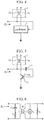
- FIG. 4 is a configuration diagram of a variable inductor circuit according to the second embodiment.
- FIG. 5 a specific example of the gm element 3 is illustrated.
- a bipolar transistor 31 is used, and a capacitor 4 is coupled for applying a DC voltage (Vbias) to the base terminal.
- Vbias DC voltage
- FIG. 6 a small signal equivalent circuit of the circuit of FIG. 5 is illustrated.
- symbols “L1” and “L2” correspond to the inductor 1a and the other inductor 1b that are magnetically coupled
- symbol “M” denotes the mutual inductance of L1 and L2.
- Symbol “C1” denotes the capacitance of the capacitor 4
- symbol “r ⁇ ” denotes the input resistance of the bipolar transistor 31
- symbol “ic denotes the collector current of the bipolar transistor 31.
- the input impedance Zin of this small signal equivalent circuit can be expressed by equation (2).
- Zin j ⁇ L 2 / / r ⁇ j 1 / ⁇ C 1 + ⁇ 2 M 2 / j ⁇ L 1 + 1 / gm
- the inductance value of the other inductor 1b can be changed by controlling r ⁇ coupled in parallel to the other inductor 1b, that is, gm.
- FIG. 7 a configuration is illustrated as a more specific circuit example in which the buffer circuit 5 is coupled as the preceding stage of an input terminal of the control voltage of the gm element 3.
- FIG. 8 illustrates a specific circuit configuration of the gm element 3 and the buffer circuit 5.
- the inductor 1a and the other inductor 1b are magnetically coupled to each other. One end of each of the inductor 1a and the other inductor 1b is coupled to a voltage source, and the other end of the inductor 1a is coupled to a cascode amplifier (first transistor 32 and second transistor 33) as the gm element 3.
- the other end of the other inductor 1b is coupled to the base terminal of the second transistor 33 via a first capacitor 6a, the buffer circuit 5 including a third transistor 34 and a fourth transistor 35 (here, an emitter follower circuit), and a second capacitor 6b.
- a control current source 7 is coupled to the collector terminal of the second transistor 33. With the cascode amplifier coupled to the inductor 1a, gm expressed by equation (2) is apparently increased, thereby expanding the variable range of the inductance value.
- the buffer circuit 5 mitigates reflection of a high-frequency voltage between point X and the second transistor 33.
- the control current source 7 can make the direct current flowing in the first transistor 32 variable, and thus is used for controlling the inductance value.
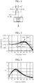
- FIGS. 9 and 10 are graphs illustrating simulation results of the inductance value and the Q value when the current value (I1) of the control current source 7 is controlled to change the current flowing in the inductor 1a.
- the vertical axis in FIG. 9 represents the inductance (Inductance [H])
- the vertical axis in FIG. 10 represents the Q value
- the horizontal axes in FIGS. 9 and 10 represent the frequency (Frequency [GHz]).
- the inductor 1a and the other inductor 1b have been described as the inductors 1 that are magnetically coupled to each other; however, similar effects can be obtained even with three inductors (the inductor 1a, the other inductor 1b, and a third inductor 1c) as illustrated in FIG. 11 .
- the third inductor 1c is coupled in parallel with the inductor 1a, and the other configuration is similar to that in FIG. 8 .
- similar effects can be obtained even when three or more inductors are targeted.
- the inductance value of one inductor is made variable by controlling the current flowing in the inductors other than that inductor.
- variable inductor circuit of the second embodiment includes: the one inductor and the other inductor magnetically coupled to each other; and the gm element for controlling the current flowing in the one inductor, in which the gm element is controlled by a terminal voltage of the other inductor, thereby controlling a current flowing in the one inductor to cause an inductance value of the other inductor to be variable. Therefore, the variable range of the inductance value can be expanded and the Q value can be improved in addition to the effects of the first embodiment.
- variable inductor circuit of the second embodiment includes: the one inductor and the other inductor magnetically coupled to each other; the cascode amplifier for controlling the current flowing in the one inductor; and the control current source coupled to the collector terminal of the transistor, the emitter of which is grounded, of the cascode amplifier, in which a high-frequency voltage is applied to the cascode amplifier from a terminal of the other inductor via the buffer circuit, and the current of the control current source is changed to change the current flowing in the cascode amplifier to cause the inductance value of the other inductor to be variable. Therefore, the variable range of the inductance value can be expanded and the Q value can be improved in addition to the effects of the first embodiment.
- variable inductor circuit of the second embodiment includes three or more inductors magnetically coupled to each other, the three or more inductors including the one inductor and the other inductor, in which the inductance value of the one inductor is made variable by controlling the current flowing in the inductors other than the one inductor out of the three or more inductors. Therefore, also for the configuration in which three or more inductors are magnetically coupled to each other, it becomes possible to suppress the mounting cost and to electrically adjust the inductance value even in a high frequency band.
- FIG. 12 is a configuration diagram of a variable inductor circuit according to the third embodiment.
- a limiting amplifier 8 is coupled instead of the buffer circuit 5 of the second embodiment illustrated in FIG. 7 .
- the gm value of the gm element 3 disadvantageously changes, thereby causing the inductance value when viewed from ZL to change.
- the limiting amplifier 8 by coupling the limiting amplifier 8 as illustrated in FIG. 12 , the gm value of the gm element 3 can be kept constant, and the inductance value when viewed from ZL can also be kept constant.
- the third embodiment can also be applied to three or more inductors like the configuration illustrated in FIG. 11 of the second embodiment.
- the inductance value of the variable inductor circuit can be kept constant even in a case where the amplitude of the high-frequency voltage input to the variable inductor circuit is not constant.
- the present invention may include a flexible combination of the respective embodiments, a modification of any component of the embodiments, or an omission of any component in the embodiments within the scope of the present invention.
- variable inductor circuit relates to a configuration for electrically adjusting an inductance value, and is suitable for use in a matching circuit of a high frequency circuit.
Landscapes
- Engineering & Computer Science (AREA)
- Power Engineering (AREA)
- Networks Using Active Elements (AREA)
Applications Claiming Priority (1)
| Application Number | Priority Date | Filing Date | Title |
|---|---|---|---|
| PCT/JP2018/009005 WO2019171539A1 (ja) | 2018-03-08 | 2018-03-08 | 可変インダクタ回路 |
Publications (3)
| Publication Number | Publication Date |
|---|---|
| EP3748848A1 true EP3748848A1 (de) | 2020-12-09 |
| EP3748848A4 EP3748848A4 (de) | 2021-02-17 |
| EP3748848B1 EP3748848B1 (de) | 2022-05-04 |
Family
ID=65655820
Family Applications (1)
| Application Number | Title | Priority Date | Filing Date |
|---|---|---|---|
| EP18909191.1A Active EP3748848B1 (de) | 2018-03-08 | 2018-03-08 | Variable induktorschaltung |
Country Status (5)
| Country | Link |
|---|---|
| US (1) | US11329632B2 (de) |
| EP (1) | EP3748848B1 (de) |
| JP (1) | JP6479280B1 (de) |
| CN (1) | CN111819793B (de) |
| WO (1) | WO2019171539A1 (de) |
Family Cites Families (21)
| Publication number | Priority date | Publication date | Assignee | Title |
|---|---|---|---|---|
| US6114930A (en) | 1995-11-27 | 2000-09-05 | Telefonaktiebolaget Lm Ericsson | Impedance controlled by the phase angle between two signals |
| SE506626C2 (sv) * | 1995-11-27 | 1998-01-19 | Ericsson Telefon Ab L M | Impedansorgan |
| US6608361B2 (en) * | 2001-07-31 | 2003-08-19 | G-Plus, Inc. | On-chip inductor using active magnetic energy recovery |
| CA2417395A1 (en) * | 2002-01-28 | 2003-07-28 | James William Haslett | Monolithic transformer compensated circuit |
| US7098737B2 (en) * | 2002-05-31 | 2006-08-29 | Kabushiki Kaisha Toshiba | Variable inductor, oscillator including the variable inductor and radio terminal comprising this oscillator, and amplifier including the variable inductor and radio terminal comprising this amplifier |
| JP4686487B2 (ja) * | 2002-05-31 | 2011-05-25 | 株式会社東芝 | 可変インダクタを含む増幅器及びこの増幅器を備えた無線端末 |
| JP3959371B2 (ja) * | 2002-05-31 | 2007-08-15 | 株式会社東芝 | 可変インダクタ |
| ITPI20030044A1 (it) * | 2003-06-09 | 2004-12-10 | Univ Pisa | Commutatore a radiofrequenza integrato basato sul |
| JP2005001263A (ja) * | 2003-06-12 | 2005-01-06 | Idemitsu Unitech Co Ltd | 製袋装置及び製袋方法 |
| GB2407214A (en) * | 2003-10-14 | 2005-04-20 | Magtech A S | Variable inductor |
| JP2006013810A (ja) * | 2004-06-24 | 2006-01-12 | Sharp Corp | 可変利得増幅回路 |
| JP2006303776A (ja) * | 2005-04-19 | 2006-11-02 | Matsushita Electric Ind Co Ltd | インダクタユニットおよびこれを用いた発振器 |
| TWI327416B (en) * | 2006-10-27 | 2010-07-11 | Nat Univ Tsing Hua | Cascode low noise amplifier with a source coupled active inductor |
| JP2010537453A (ja) * | 2007-09-14 | 2010-12-02 | 富士通株式会社 | チューナブルインピーダンス整合回路 |
| JP2009152254A (ja) * | 2007-12-19 | 2009-07-09 | Tokyo Institute Of Technology | オンチップ可変インダクタ |
| US20090251218A1 (en) * | 2008-04-03 | 2009-10-08 | Paulo Oliveira | Variable Gain Amplifier |
| US8766746B2 (en) | 2011-09-21 | 2014-07-01 | Fujitsu Limited | Active inductor |
| JP6036564B2 (ja) | 2013-06-14 | 2016-11-30 | 富士通株式会社 | 可変インダクタ回路及び高周波回路 |
| US9853614B2 (en) * | 2014-12-04 | 2017-12-26 | Qualcomm Incorporated | Amplifier with triple-coupled inductors |
| EP3125065B1 (de) * | 2015-07-31 | 2018-12-19 | Power Integrations Switzerland GmbH | Kommunikation über galvanische isolierung hinweg |
| CN107707217B (zh) * | 2017-11-17 | 2021-06-08 | 西安电子科技大学 | 高dB增益的宽带变跨导六位有源移相器 |
-
2018
- 2018-03-08 EP EP18909191.1A patent/EP3748848B1/de active Active
- 2018-03-08 WO PCT/JP2018/009005 patent/WO2019171539A1/ja not_active Ceased
- 2018-03-08 CN CN201880090388.5A patent/CN111819793B/zh active Active
- 2018-03-08 JP JP2018539451A patent/JP6479280B1/ja active Active
-
2020
- 2020-08-14 US US16/994,102 patent/US11329632B2/en active Active
Also Published As
| Publication number | Publication date |
|---|---|
| WO2019171539A1 (ja) | 2019-09-12 |
| US20200373912A1 (en) | 2020-11-26 |
| JPWO2019171539A1 (ja) | 2020-04-16 |
| CN111819793B (zh) | 2023-09-12 |
| EP3748848A4 (de) | 2021-02-17 |
| US11329632B2 (en) | 2022-05-10 |
| EP3748848B1 (de) | 2022-05-04 |
| JP6479280B1 (ja) | 2019-03-06 |
| CN111819793A (zh) | 2020-10-23 |
Similar Documents
| Publication | Publication Date | Title |
|---|---|---|
| JP4402143B2 (ja) | 発振器及びそれを用いた通信システム | |
| US7521996B2 (en) | Differential amplifier and radio system with a differential amplifier | |
| CN103168354B (zh) | 电感器 | |
| JP2001160723A (ja) | 分布増幅器 | |
| CN109546980B (zh) | 功率放大电路 | |
| JP3545142B2 (ja) | 差動増幅器 | |
| JP5267407B2 (ja) | 増幅回路及び通信装置 | |
| US20070046378A1 (en) | Operational amplifier output stage and method | |
| CN107026621B (zh) | 功率放大器系统和相关的偏置电路 | |
| US7123097B2 (en) | Ultra-wideband constant gain CMOS amplifier | |
| KR101661151B1 (ko) | 테이퍼링된 캐패시터를 갖는 비균일 분산 전력 증폭기 | |
| US6437612B1 (en) | Inductor-less RF/IF CMOS buffer for 50Ω off-chip load driving | |
| US11329632B2 (en) | Variable inductor circuit | |
| JP2006005848A (ja) | 電力増幅器及び高周波通信装置 | |
| JP2021090168A (ja) | 電力増幅回路 | |
| JP2022036784A (ja) | 受信回路及び光受信回路 | |
| JP2001251150A (ja) | 単相信号/差動信号変換型の電圧増幅器 | |
| JP6470213B2 (ja) | 可変利得増幅器 | |
| KR100866235B1 (ko) | Q 향상 회로 및 방법 | |
| EP2814171A2 (de) | Variable Induktivitätsschaltung und Hochfrequenzschaltung | |
| Shukla | New Circuit Model of Small-Signal Amplifiers with Darlington pairs under Sziklai pair Topology | |
| Meharde et al. | Low voltage CMOS active inductor with bandwidth and linearity improvement | |
| JP7711573B2 (ja) | 増幅器 | |
| US20250023523A1 (en) | Peaking adjustment circuit | |
| KR102438992B1 (ko) | 전압 제어 발진 회로 |
Legal Events
| Date | Code | Title | Description |
|---|---|---|---|
| STAA | Information on the status of an ep patent application or granted ep patent |
Free format text: STATUS: THE INTERNATIONAL PUBLICATION HAS BEEN MADE |
|
| PUAI | Public reference made under article 153(3) epc to a published international application that has entered the european phase |
Free format text: ORIGINAL CODE: 0009012 |
|
| STAA | Information on the status of an ep patent application or granted ep patent |
Free format text: STATUS: REQUEST FOR EXAMINATION WAS MADE |
|
| 17P | Request for examination filed |
Effective date: 20200821 |
|
| AK | Designated contracting states |
Kind code of ref document: A1 Designated state(s): AL AT BE BG CH CY CZ DE DK EE ES FI FR GB GR HR HU IE IS IT LI LT LU LV MC MK MT NL NO PL PT RO RS SE SI SK SM TR |
|
| AX | Request for extension of the european patent |
Extension state: BA ME |
|
| A4 | Supplementary search report drawn up and despatched |
Effective date: 20210115 |
|
| RIC1 | Information provided on ipc code assigned before grant |
Ipc: H03H 11/28 20060101ALI20210111BHEP Ipc: H03H 11/48 20060101AFI20210111BHEP Ipc: H03H 7/09 20060101ALN20210111BHEP |
|
| DAV | Request for validation of the european patent (deleted) | ||
| DAX | Request for extension of the european patent (deleted) | ||
| REG | Reference to a national code |
Ref country code: DE Ref legal event code: R079 Ref document number: 602018035210 Country of ref document: DE Free format text: PREVIOUS MAIN CLASS: H03H0011460000 Ipc: H03H0011480000 |
|
| GRAP | Despatch of communication of intention to grant a patent |
Free format text: ORIGINAL CODE: EPIDOSNIGR1 |
|
| STAA | Information on the status of an ep patent application or granted ep patent |
Free format text: STATUS: GRANT OF PATENT IS INTENDED |
|
| RIC1 | Information provided on ipc code assigned before grant |
Ipc: H03H 7/09 20060101ALN20211018BHEP Ipc: H03H 11/28 20060101ALI20211018BHEP Ipc: H03H 11/48 20060101AFI20211018BHEP |
|
| INTG | Intention to grant announced |
Effective date: 20211118 |
|
| GRAS | Grant fee paid |
Free format text: ORIGINAL CODE: EPIDOSNIGR3 |
|
| GRAA | (expected) grant |
Free format text: ORIGINAL CODE: 0009210 |
|
| STAA | Information on the status of an ep patent application or granted ep patent |
Free format text: STATUS: THE PATENT HAS BEEN GRANTED |
|
| AK | Designated contracting states |
Kind code of ref document: B1 Designated state(s): AL AT BE BG CH CY CZ DE DK EE ES FI FR GB GR HR HU IE IS IT LI LT LU LV MC MK MT NL NO PL PT RO RS SE SI SK SM TR |
|
| REG | Reference to a national code |
Ref country code: GB Ref legal event code: FG4D |
|
| REG | Reference to a national code |
Ref country code: CH Ref legal event code: EP |
|
| REG | Reference to a national code |
Ref country code: AT Ref legal event code: REF Ref document number: 1490219 Country of ref document: AT Kind code of ref document: T Effective date: 20220515 |
|
| REG | Reference to a national code |
Ref country code: IE Ref legal event code: FG4D Ref country code: DE Ref legal event code: R096 Ref document number: 602018035210 Country of ref document: DE |
|
| REG | Reference to a national code |
Ref country code: LT Ref legal event code: MG9D |
|
| REG | Reference to a national code |
Ref country code: NL Ref legal event code: MP Effective date: 20220504 |
|
| REG | Reference to a national code |
Ref country code: AT Ref legal event code: MK05 Ref document number: 1490219 Country of ref document: AT Kind code of ref document: T Effective date: 20220504 |
|
| PG25 | Lapsed in a contracting state [announced via postgrant information from national office to epo] |
Ref country code: SE Free format text: LAPSE BECAUSE OF FAILURE TO SUBMIT A TRANSLATION OF THE DESCRIPTION OR TO PAY THE FEE WITHIN THE PRESCRIBED TIME-LIMIT Effective date: 20220504 Ref country code: PT Free format text: LAPSE BECAUSE OF FAILURE TO SUBMIT A TRANSLATION OF THE DESCRIPTION OR TO PAY THE FEE WITHIN THE PRESCRIBED TIME-LIMIT Effective date: 20220905 Ref country code: NO Free format text: LAPSE BECAUSE OF FAILURE TO SUBMIT A TRANSLATION OF THE DESCRIPTION OR TO PAY THE FEE WITHIN THE PRESCRIBED TIME-LIMIT Effective date: 20220804 Ref country code: NL Free format text: LAPSE BECAUSE OF FAILURE TO SUBMIT A TRANSLATION OF THE DESCRIPTION OR TO PAY THE FEE WITHIN THE PRESCRIBED TIME-LIMIT Effective date: 20220504 Ref country code: LT Free format text: LAPSE BECAUSE OF FAILURE TO SUBMIT A TRANSLATION OF THE DESCRIPTION OR TO PAY THE FEE WITHIN THE PRESCRIBED TIME-LIMIT Effective date: 20220504 Ref country code: HR Free format text: LAPSE BECAUSE OF FAILURE TO SUBMIT A TRANSLATION OF THE DESCRIPTION OR TO PAY THE FEE WITHIN THE PRESCRIBED TIME-LIMIT Effective date: 20220504 Ref country code: GR Free format text: LAPSE BECAUSE OF FAILURE TO SUBMIT A TRANSLATION OF THE DESCRIPTION OR TO PAY THE FEE WITHIN THE PRESCRIBED TIME-LIMIT Effective date: 20220805 Ref country code: FI Free format text: LAPSE BECAUSE OF FAILURE TO SUBMIT A TRANSLATION OF THE DESCRIPTION OR TO PAY THE FEE WITHIN THE PRESCRIBED TIME-LIMIT Effective date: 20220504 Ref country code: BG Free format text: LAPSE BECAUSE OF FAILURE TO SUBMIT A TRANSLATION OF THE DESCRIPTION OR TO PAY THE FEE WITHIN THE PRESCRIBED TIME-LIMIT Effective date: 20220804 Ref country code: AT Free format text: LAPSE BECAUSE OF FAILURE TO SUBMIT A TRANSLATION OF THE DESCRIPTION OR TO PAY THE FEE WITHIN THE PRESCRIBED TIME-LIMIT Effective date: 20220504 |
|
| PG25 | Lapsed in a contracting state [announced via postgrant information from national office to epo] |
Ref country code: RS Free format text: LAPSE BECAUSE OF FAILURE TO SUBMIT A TRANSLATION OF THE DESCRIPTION OR TO PAY THE FEE WITHIN THE PRESCRIBED TIME-LIMIT Effective date: 20220504 Ref country code: PL Free format text: LAPSE BECAUSE OF FAILURE TO SUBMIT A TRANSLATION OF THE DESCRIPTION OR TO PAY THE FEE WITHIN THE PRESCRIBED TIME-LIMIT Effective date: 20220504 Ref country code: LV Free format text: LAPSE BECAUSE OF FAILURE TO SUBMIT A TRANSLATION OF THE DESCRIPTION OR TO PAY THE FEE WITHIN THE PRESCRIBED TIME-LIMIT Effective date: 20220504 Ref country code: IS Free format text: LAPSE BECAUSE OF FAILURE TO SUBMIT A TRANSLATION OF THE DESCRIPTION OR TO PAY THE FEE WITHIN THE PRESCRIBED TIME-LIMIT Effective date: 20220904 |
|
| PG25 | Lapsed in a contracting state [announced via postgrant information from national office to epo] |
Ref country code: SM Free format text: LAPSE BECAUSE OF FAILURE TO SUBMIT A TRANSLATION OF THE DESCRIPTION OR TO PAY THE FEE WITHIN THE PRESCRIBED TIME-LIMIT Effective date: 20220504 Ref country code: SK Free format text: LAPSE BECAUSE OF FAILURE TO SUBMIT A TRANSLATION OF THE DESCRIPTION OR TO PAY THE FEE WITHIN THE PRESCRIBED TIME-LIMIT Effective date: 20220504 Ref country code: RO Free format text: LAPSE BECAUSE OF FAILURE TO SUBMIT A TRANSLATION OF THE DESCRIPTION OR TO PAY THE FEE WITHIN THE PRESCRIBED TIME-LIMIT Effective date: 20220504 Ref country code: ES Free format text: LAPSE BECAUSE OF FAILURE TO SUBMIT A TRANSLATION OF THE DESCRIPTION OR TO PAY THE FEE WITHIN THE PRESCRIBED TIME-LIMIT Effective date: 20220504 Ref country code: EE Free format text: LAPSE BECAUSE OF FAILURE TO SUBMIT A TRANSLATION OF THE DESCRIPTION OR TO PAY THE FEE WITHIN THE PRESCRIBED TIME-LIMIT Effective date: 20220504 Ref country code: DK Free format text: LAPSE BECAUSE OF FAILURE TO SUBMIT A TRANSLATION OF THE DESCRIPTION OR TO PAY THE FEE WITHIN THE PRESCRIBED TIME-LIMIT Effective date: 20220504 Ref country code: CZ Free format text: LAPSE BECAUSE OF FAILURE TO SUBMIT A TRANSLATION OF THE DESCRIPTION OR TO PAY THE FEE WITHIN THE PRESCRIBED TIME-LIMIT Effective date: 20220504 |
|
| REG | Reference to a national code |
Ref country code: DE Ref legal event code: R097 Ref document number: 602018035210 Country of ref document: DE |
|
| PLBE | No opposition filed within time limit |
Free format text: ORIGINAL CODE: 0009261 |
|
| STAA | Information on the status of an ep patent application or granted ep patent |
Free format text: STATUS: NO OPPOSITION FILED WITHIN TIME LIMIT |
|
| PG25 | Lapsed in a contracting state [announced via postgrant information from national office to epo] |
Ref country code: AL Free format text: LAPSE BECAUSE OF FAILURE TO SUBMIT A TRANSLATION OF THE DESCRIPTION OR TO PAY THE FEE WITHIN THE PRESCRIBED TIME-LIMIT Effective date: 20220504 |
|
| 26N | No opposition filed |
Effective date: 20230207 |
|
| PG25 | Lapsed in a contracting state [announced via postgrant information from national office to epo] |
Ref country code: SI Free format text: LAPSE BECAUSE OF FAILURE TO SUBMIT A TRANSLATION OF THE DESCRIPTION OR TO PAY THE FEE WITHIN THE PRESCRIBED TIME-LIMIT Effective date: 20220504 |
|
| P01 | Opt-out of the competence of the unified patent court (upc) registered |
Effective date: 20230512 |
|
| PG25 | Lapsed in a contracting state [announced via postgrant information from national office to epo] |
Ref country code: MC Free format text: LAPSE BECAUSE OF FAILURE TO SUBMIT A TRANSLATION OF THE DESCRIPTION OR TO PAY THE FEE WITHIN THE PRESCRIBED TIME-LIMIT Effective date: 20220504 |
|
| REG | Reference to a national code |
Ref country code: CH Ref legal event code: PL |
|
| REG | Reference to a national code |
Ref country code: BE Ref legal event code: MM Effective date: 20230331 |
|
| PG25 | Lapsed in a contracting state [announced via postgrant information from national office to epo] |
Ref country code: LU Free format text: LAPSE BECAUSE OF NON-PAYMENT OF DUE FEES Effective date: 20230308 |
|
| REG | Reference to a national code |
Ref country code: IE Ref legal event code: MM4A |
|
| PG25 | Lapsed in a contracting state [announced via postgrant information from national office to epo] |
Ref country code: LI Free format text: LAPSE BECAUSE OF NON-PAYMENT OF DUE FEES Effective date: 20230331 Ref country code: IT Free format text: LAPSE BECAUSE OF FAILURE TO SUBMIT A TRANSLATION OF THE DESCRIPTION OR TO PAY THE FEE WITHIN THE PRESCRIBED TIME-LIMIT Effective date: 20220504 Ref country code: IE Free format text: LAPSE BECAUSE OF NON-PAYMENT OF DUE FEES Effective date: 20230308 Ref country code: CH Free format text: LAPSE BECAUSE OF NON-PAYMENT OF DUE FEES Effective date: 20230331 |
|
| PG25 | Lapsed in a contracting state [announced via postgrant information from national office to epo] |
Ref country code: BE Free format text: LAPSE BECAUSE OF NON-PAYMENT OF DUE FEES Effective date: 20230331 |
|
| REG | Reference to a national code |
Ref country code: DE Ref legal event code: R084 Ref document number: 602018035210 Country of ref document: DE |
|
| REG | Reference to a national code |
Ref country code: GB Ref legal event code: 746 Effective date: 20240531 |
|
| PG25 | Lapsed in a contracting state [announced via postgrant information from national office to epo] |
Ref country code: BG Free format text: LAPSE BECAUSE OF FAILURE TO SUBMIT A TRANSLATION OF THE DESCRIPTION OR TO PAY THE FEE WITHIN THE PRESCRIBED TIME-LIMIT Effective date: 20220504 |
|
| PG25 | Lapsed in a contracting state [announced via postgrant information from national office to epo] |
Ref country code: BG Free format text: LAPSE BECAUSE OF FAILURE TO SUBMIT A TRANSLATION OF THE DESCRIPTION OR TO PAY THE FEE WITHIN THE PRESCRIBED TIME-LIMIT Effective date: 20220504 |
|
| PG25 | Lapsed in a contracting state [announced via postgrant information from national office to epo] |
Ref country code: CY Free format text: LAPSE BECAUSE OF FAILURE TO SUBMIT A TRANSLATION OF THE DESCRIPTION OR TO PAY THE FEE WITHIN THE PRESCRIBED TIME-LIMIT; INVALID AB INITIO Effective date: 20180308 |
|
| PG25 | Lapsed in a contracting state [announced via postgrant information from national office to epo] |
Ref country code: HU Free format text: LAPSE BECAUSE OF FAILURE TO SUBMIT A TRANSLATION OF THE DESCRIPTION OR TO PAY THE FEE WITHIN THE PRESCRIBED TIME-LIMIT; INVALID AB INITIO Effective date: 20180308 |
|
| PG25 | Lapsed in a contracting state [announced via postgrant information from national office to epo] |
Ref country code: TR Free format text: LAPSE BECAUSE OF FAILURE TO SUBMIT A TRANSLATION OF THE DESCRIPTION OR TO PAY THE FEE WITHIN THE PRESCRIBED TIME-LIMIT Effective date: 20220504 |
|
| PGFP | Annual fee paid to national office [announced via postgrant information from national office to epo] |
Ref country code: GB Payment date: 20260202 Year of fee payment: 9 |
|
| PGFP | Annual fee paid to national office [announced via postgrant information from national office to epo] |
Ref country code: DE Payment date: 20260128 Year of fee payment: 9 |
|
| PGFP | Annual fee paid to national office [announced via postgrant information from national office to epo] |
Ref country code: FR Payment date: 20260209 Year of fee payment: 9 |