EP3736626B1 - Liquid crystal antenna and manufacturing method therefor - Google Patents
Liquid crystal antenna and manufacturing method therefor Download PDFInfo
- Publication number
- EP3736626B1 EP3736626B1 EP19863991.6A EP19863991A EP3736626B1 EP 3736626 B1 EP3736626 B1 EP 3736626B1 EP 19863991 A EP19863991 A EP 19863991A EP 3736626 B1 EP3736626 B1 EP 3736626B1
- Authority
- EP
- European Patent Office
- Prior art keywords
- substrate
- layer
- metal film
- liquid crystal
- film layer
- Prior art date
- Legal status (The legal status is an assumption and is not a legal conclusion. Google has not performed a legal analysis and makes no representation as to the accuracy of the status listed.)
- Active
Links
- 239000004973 liquid crystal related substance Substances 0.000 title claims description 92
- 238000004519 manufacturing process Methods 0.000 title claims description 36
- 229910052751 metal Inorganic materials 0.000 claims description 181
- 239000002184 metal Substances 0.000 claims description 181
- 239000000758 substrate Substances 0.000 claims description 180
- 238000000034 method Methods 0.000 claims description 85
- 238000007747 plating Methods 0.000 claims description 50
- RYGMFSIKBFXOCR-UHFFFAOYSA-N Copper Chemical compound [Cu] RYGMFSIKBFXOCR-UHFFFAOYSA-N 0.000 claims description 26
- 229910052802 copper Inorganic materials 0.000 claims description 26
- 239000010949 copper Substances 0.000 claims description 26
- 239000011521 glass Substances 0.000 claims description 26
- 238000009713 electroplating Methods 0.000 claims description 23
- 238000005234 chemical deposition Methods 0.000 claims description 22
- 239000000463 material Substances 0.000 claims description 13
- 229910044991 metal oxide Inorganic materials 0.000 claims description 13
- 150000004706 metal oxides Chemical class 0.000 claims description 13
- 239000007769 metal material Substances 0.000 claims description 12
- 238000000059 patterning Methods 0.000 claims description 9
- 238000007654 immersion Methods 0.000 claims description 8
- 238000004140 cleaning Methods 0.000 claims description 6
- 230000035699 permeability Effects 0.000 claims description 5
- 239000002245 particle Substances 0.000 claims description 2
- 239000010408 film Substances 0.000 description 136
- 230000008569 process Effects 0.000 description 38
- 230000005855 radiation Effects 0.000 description 14
- 239000004020 conductor Substances 0.000 description 12
- 229920002120 photoresistant polymer Polymers 0.000 description 12
- 238000001755 magnetron sputter deposition Methods 0.000 description 11
- 239000000126 substance Substances 0.000 description 11
- BQCADISMDOOEFD-UHFFFAOYSA-N Silver Chemical compound [Ag] BQCADISMDOOEFD-UHFFFAOYSA-N 0.000 description 8
- 238000005229 chemical vapour deposition Methods 0.000 description 8
- 239000000565 sealant Substances 0.000 description 8
- 229910052709 silver Inorganic materials 0.000 description 8
- 239000004332 silver Substances 0.000 description 8
- 229910052782 aluminium Inorganic materials 0.000 description 7
- XAGFODPZIPBFFR-UHFFFAOYSA-N aluminium Chemical compound [Al] XAGFODPZIPBFFR-UHFFFAOYSA-N 0.000 description 7
- 230000002500 effect on skin Effects 0.000 description 7
- PCHJSUWPFVWCPO-UHFFFAOYSA-N gold Chemical compound [Au] PCHJSUWPFVWCPO-UHFFFAOYSA-N 0.000 description 7
- 229910052737 gold Inorganic materials 0.000 description 7
- 239000010931 gold Substances 0.000 description 7
- 230000000717 retained effect Effects 0.000 description 7
- 238000004891 communication Methods 0.000 description 6
- 210000002858 crystal cell Anatomy 0.000 description 6
- 239000007788 liquid Substances 0.000 description 6
- 229910045601 alloy Inorganic materials 0.000 description 5
- 239000000956 alloy Substances 0.000 description 5
- 230000005540 biological transmission Effects 0.000 description 5
- 238000000151 deposition Methods 0.000 description 5
- KDLHZDBZIXYQEI-UHFFFAOYSA-N Palladium Chemical compound [Pd] KDLHZDBZIXYQEI-UHFFFAOYSA-N 0.000 description 4
- 238000001035 drying Methods 0.000 description 4
- 230000000694 effects Effects 0.000 description 4
- 238000005516 engineering process Methods 0.000 description 4
- 238000010586 diagram Methods 0.000 description 3
- 230000005684 electric field Effects 0.000 description 3
- 230000008020 evaporation Effects 0.000 description 3
- 238000001704 evaporation Methods 0.000 description 3
- 230000035882 stress Effects 0.000 description 3
- XEEYBQQBJWHFJM-UHFFFAOYSA-N Iron Chemical compound [Fe] XEEYBQQBJWHFJM-UHFFFAOYSA-N 0.000 description 2
- PXHVJJICTQNCMI-UHFFFAOYSA-N Nickel Chemical compound [Ni] PXHVJJICTQNCMI-UHFFFAOYSA-N 0.000 description 2
- 230000009286 beneficial effect Effects 0.000 description 2
- 230000003197 catalytic effect Effects 0.000 description 2
- 238000006243 chemical reaction Methods 0.000 description 2
- 239000000428 dust Substances 0.000 description 2
- 238000005530 etching Methods 0.000 description 2
- 230000006872 improvement Effects 0.000 description 2
- 238000011031 large-scale manufacturing process Methods 0.000 description 2
- 229910021645 metal ion Inorganic materials 0.000 description 2
- 239000002923 metal particle Substances 0.000 description 2
- 229910052763 palladium Inorganic materials 0.000 description 2
- 238000006479 redox reaction Methods 0.000 description 2
- 238000000859 sublimation Methods 0.000 description 2
- 230000008022 sublimation Effects 0.000 description 2
- 230000008646 thermal stress Effects 0.000 description 2
- VYZAMTAEIAYCRO-UHFFFAOYSA-N Chromium Chemical compound [Cr] VYZAMTAEIAYCRO-UHFFFAOYSA-N 0.000 description 1
- QPLDLSVMHZLSFG-UHFFFAOYSA-N Copper oxide Chemical compound [Cu]=O QPLDLSVMHZLSFG-UHFFFAOYSA-N 0.000 description 1
- 239000005751 Copper oxide Substances 0.000 description 1
- ZOKXTWBITQBERF-UHFFFAOYSA-N Molybdenum Chemical compound [Mo] ZOKXTWBITQBERF-UHFFFAOYSA-N 0.000 description 1
- GWEVSGVZZGPLCZ-UHFFFAOYSA-N Titan oxide Chemical compound O=[Ti]=O GWEVSGVZZGPLCZ-UHFFFAOYSA-N 0.000 description 1
- 230000004308 accommodation Effects 0.000 description 1
- 230000009471 action Effects 0.000 description 1
- 238000007605 air drying Methods 0.000 description 1
- WYTGDNHDOZPMIW-RCBQFDQVSA-N alstonine Natural products C1=CC2=C3C=CC=CC3=NC2=C2N1C[C@H]1[C@H](C)OC=C(C(=O)OC)[C@H]1C2 WYTGDNHDOZPMIW-RCBQFDQVSA-N 0.000 description 1
- 238000005452 bending Methods 0.000 description 1
- 230000015572 biosynthetic process Effects 0.000 description 1
- 229910052793 cadmium Inorganic materials 0.000 description 1
- BDOSMKKIYDKNTQ-UHFFFAOYSA-N cadmium atom Chemical compound [Cd] BDOSMKKIYDKNTQ-UHFFFAOYSA-N 0.000 description 1
- 239000000919 ceramic Substances 0.000 description 1
- 229910010293 ceramic material Inorganic materials 0.000 description 1
- 229910052804 chromium Inorganic materials 0.000 description 1
- 239000011651 chromium Substances 0.000 description 1
- 239000002131 composite material Substances 0.000 description 1
- 150000001875 compounds Chemical class 0.000 description 1
- 229910000431 copper oxide Inorganic materials 0.000 description 1
- 230000007123 defense Effects 0.000 description 1
- 238000011161 development Methods 0.000 description 1
- 238000009826 distribution Methods 0.000 description 1
- 238000000469 dry deposition Methods 0.000 description 1
- 238000003487 electrochemical reaction Methods 0.000 description 1
- 230000005672 electromagnetic field Effects 0.000 description 1
- 150000004678 hydrides Chemical class 0.000 description 1
- 238000003780 insertion Methods 0.000 description 1
- 230000037431 insertion Effects 0.000 description 1
- 238000009413 insulation Methods 0.000 description 1
- 229910052742 iron Inorganic materials 0.000 description 1
- 150000001247 metal acetylides Chemical class 0.000 description 1
- 239000000203 mixture Substances 0.000 description 1
- 238000012986 modification Methods 0.000 description 1
- 230000004048 modification Effects 0.000 description 1
- 229910052750 molybdenum Inorganic materials 0.000 description 1
- 239000011733 molybdenum Substances 0.000 description 1
- 229910052759 nickel Inorganic materials 0.000 description 1
- 229910000480 nickel oxide Inorganic materials 0.000 description 1
- 229910052758 niobium Inorganic materials 0.000 description 1
- 239000010955 niobium Substances 0.000 description 1
- GUCVJGMIXFAOAE-UHFFFAOYSA-N niobium atom Chemical compound [Nb] GUCVJGMIXFAOAE-UHFFFAOYSA-N 0.000 description 1
- 150000004767 nitrides Chemical class 0.000 description 1
- 238000007254 oxidation reaction Methods 0.000 description 1
- -1 oxides Chemical class 0.000 description 1
- GNRSAWUEBMWBQH-UHFFFAOYSA-N oxonickel Chemical compound [Ni]=O GNRSAWUEBMWBQH-UHFFFAOYSA-N 0.000 description 1
- 230000010363 phase shift Effects 0.000 description 1
- 238000005240 physical vapour deposition Methods 0.000 description 1
- 239000010453 quartz Substances 0.000 description 1
- 238000007789 sealing Methods 0.000 description 1
- 230000008054 signal transmission Effects 0.000 description 1
- VYPSYNLAJGMNEJ-UHFFFAOYSA-N silicon dioxide Inorganic materials O=[Si]=O VYPSYNLAJGMNEJ-UHFFFAOYSA-N 0.000 description 1
- 238000006467 substitution reaction Methods 0.000 description 1
- 229920001187 thermosetting polymer Polymers 0.000 description 1
- 239000004634 thermosetting polymer Substances 0.000 description 1
- 239000010409 thin film Substances 0.000 description 1
- 150000003568 thioethers Chemical class 0.000 description 1
- XOLBLPGZBRYERU-UHFFFAOYSA-N tin dioxide Chemical compound O=[Sn]=O XOLBLPGZBRYERU-UHFFFAOYSA-N 0.000 description 1
- 229910001887 tin oxide Inorganic materials 0.000 description 1
- OGIDPMRJRNCKJF-UHFFFAOYSA-N titanium oxide Inorganic materials [Ti]=O OGIDPMRJRNCKJF-UHFFFAOYSA-N 0.000 description 1
- 238000012546 transfer Methods 0.000 description 1
Images

Classifications
-
- H—ELECTRICITY
- H01—ELECTRIC ELEMENTS
- H01Q—ANTENNAS, i.e. RADIO AERIALS
- H01Q1/00—Details of, or arrangements associated with, antennas
- H01Q1/36—Structural form of radiating elements, e.g. cone, spiral, umbrella; Particular materials used therewith
- H01Q1/38—Structural form of radiating elements, e.g. cone, spiral, umbrella; Particular materials used therewith formed by a conductive layer on an insulating support
-
- G—PHYSICS
- G02—OPTICS
- G02F—OPTICAL DEVICES OR ARRANGEMENTS FOR THE CONTROL OF LIGHT BY MODIFICATION OF THE OPTICAL PROPERTIES OF THE MEDIA OF THE ELEMENTS INVOLVED THEREIN; NON-LINEAR OPTICS; FREQUENCY-CHANGING OF LIGHT; OPTICAL LOGIC ELEMENTS; OPTICAL ANALOGUE/DIGITAL CONVERTERS
- G02F1/00—Devices or arrangements for the control of the intensity, colour, phase, polarisation or direction of light arriving from an independent light source, e.g. switching, gating or modulating; Non-linear optics
- G02F1/01—Devices or arrangements for the control of the intensity, colour, phase, polarisation or direction of light arriving from an independent light source, e.g. switching, gating or modulating; Non-linear optics for the control of the intensity, phase, polarisation or colour
- G02F1/13—Devices or arrangements for the control of the intensity, colour, phase, polarisation or direction of light arriving from an independent light source, e.g. switching, gating or modulating; Non-linear optics for the control of the intensity, phase, polarisation or colour based on liquid crystals, e.g. single liquid crystal display cells
- G02F1/1313—Devices or arrangements for the control of the intensity, colour, phase, polarisation or direction of light arriving from an independent light source, e.g. switching, gating or modulating; Non-linear optics for the control of the intensity, phase, polarisation or colour based on liquid crystals, e.g. single liquid crystal display cells specially adapted for a particular application
-
- G—PHYSICS
- G02—OPTICS
- G02F—OPTICAL DEVICES OR ARRANGEMENTS FOR THE CONTROL OF LIGHT BY MODIFICATION OF THE OPTICAL PROPERTIES OF THE MEDIA OF THE ELEMENTS INVOLVED THEREIN; NON-LINEAR OPTICS; FREQUENCY-CHANGING OF LIGHT; OPTICAL LOGIC ELEMENTS; OPTICAL ANALOGUE/DIGITAL CONVERTERS
- G02F1/00—Devices or arrangements for the control of the intensity, colour, phase, polarisation or direction of light arriving from an independent light source, e.g. switching, gating or modulating; Non-linear optics
- G02F1/01—Devices or arrangements for the control of the intensity, colour, phase, polarisation or direction of light arriving from an independent light source, e.g. switching, gating or modulating; Non-linear optics for the control of the intensity, phase, polarisation or colour
- G02F1/13—Devices or arrangements for the control of the intensity, colour, phase, polarisation or direction of light arriving from an independent light source, e.g. switching, gating or modulating; Non-linear optics for the control of the intensity, phase, polarisation or colour based on liquid crystals, e.g. single liquid crystal display cells
- G02F1/133—Constructional arrangements; Operation of liquid crystal cells; Circuit arrangements
- G02F1/1333—Constructional arrangements; Manufacturing methods
- G02F1/1343—Electrodes
- G02F1/13439—Electrodes characterised by their electrical, optical, physical properties; materials therefor; method of making
-
- H—ELECTRICITY
- H01—ELECTRIC ELEMENTS
- H01Q—ANTENNAS, i.e. RADIO AERIALS
- H01Q1/00—Details of, or arrangements associated with, antennas
- H01Q1/36—Structural form of radiating elements, e.g. cone, spiral, umbrella; Particular materials used therewith
- H01Q1/364—Structural form of radiating elements, e.g. cone, spiral, umbrella; Particular materials used therewith using a particular conducting material, e.g. superconductor
Definitions
- phased array antenna has this performance index, but based on the national defense application background and chip manufacturing technology, the expensive production cost and high power consumption of the phased array antenna make it unaffordable for consumers in the consumer market, thus causing obstacles to the popularization of consumer products.
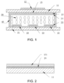
- the first substrate 11, the second substrate 21, the liquid crystal layer 30, a first conductive layer, and a second conductive layer constitute a liquid crystal phase shifter.
- the liquid crystal antenna further includes an antenna radiation unit.
- the antenna radiation unit is used for radiating microwave signals to realize the feed-in and feed-out of microwave signals.
- the antenna radiation unit is disposed on one side, away from the second substrate 21, of the first substrate 11.
- the liquid crystal antenna also includes an offset line.
- the offset line may be disposed on the second metal film layer of the second substrate.
- the electric field drives deflection of the direction of the liquid crystal molecules in the liquid crystal layer 30.
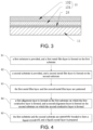
- the first metal film layer 13 can be patterned as follows: the first metal film layer 13 is coated with a layer of photoresist; the photoresist is exposed by using a mask plate to form a photoresist non-retained area and a photoresist retained area, wherein the photoresist retained area corresponds to the area where a pattern of the first conductive layer is located, and the photoresist non-retained area corresponds to the area other than the above pattern; development is conducted, wherein the photoresist in the photoresist non-retained area is completely removed, and the thickness of the photoresist in the photoresist retained area remains unchanged; the conductive layer in the photoresist non-retained area is completely etched away through etching; and the remaining photoresist is stripped to form the pattern of the first conductive layer.
- the above method for plating the glass substrates further includes performing a first baking treatment after the seed layers 24 are generated in step (b) and before the seed layers 24 are activated in step (c).
- the process of electroplating or the chemically deposited layer 131 uses the principles of electrochemical reactions to transfer metal ions to the surface of the substrate through the current effect and stack the metal ions. As it is difficult to accurately stack metal atoms, the result of the process is that the porosity of the metal film layer is high, and the atoms are not closely arranged. Through baking, the metal atoms are stacked and arranged again under thermal stress at a high temperature, so that the metal atoms are closer, the attraction force between the atoms is greater, and the metal compactness and adhesion of the chemically deposited layers 131 are enhanced.
Applications Claiming Priority (2)
| Application Number | Priority Date | Filing Date | Title |
|---|---|---|---|
| CN201910185803.1A CN109818150A (zh) | 2019-03-12 | 2019-03-12 | 一种液晶天线及其制作方法 |
| PCT/CN2019/078174 WO2020181558A1 (zh) | 2019-03-12 | 2019-03-14 | 一种液晶天线及其制作方法 |
Publications (3)
| Publication Number | Publication Date |
|---|---|
| EP3736626A1 EP3736626A1 (en) | 2020-11-11 |
| EP3736626A4 EP3736626A4 (en) | 2020-11-11 |
| EP3736626B1 true EP3736626B1 (en) | 2023-09-06 |
Family
ID=66608794
Family Applications (1)
| Application Number | Title | Priority Date | Filing Date |
|---|---|---|---|
| EP19863991.6A Active EP3736626B1 (en) | 2019-03-12 | 2019-03-14 | Liquid crystal antenna and manufacturing method therefor |
Country Status (7)
| Country | Link |
|---|---|
| US (1) | US11156859B2 (ja) |
| EP (1) | EP3736626B1 (ja) |
| JP (1) | JP6992185B2 (ja) |
| KR (1) | KR102326746B1 (ja) |
| CN (1) | CN109818150A (ja) |
| TW (1) | TWI721822B (ja) |
| WO (1) | WO2020181558A1 (ja) |
Families Citing this family (19)
| Publication number | Priority date | Publication date | Assignee | Title |
|---|---|---|---|---|
| CN112018518A (zh) * | 2019-05-29 | 2020-12-01 | 富泰华工业(深圳)有限公司 | 天线阵列及具有所述天线阵列的液晶显示器 |
| CN111430894B (zh) * | 2020-04-01 | 2021-08-03 | 电子科技大学 | 一种共形液晶光学相控阵的光学装置 |
| US20210313705A1 (en) * | 2020-04-03 | 2021-10-07 | Kymeta Corporation | Rf element design for improved tuning range |
| CN111525264B (zh) * | 2020-05-21 | 2022-01-18 | 信利(仁寿)高端显示科技有限公司 | 一种液晶天线 |
| CN113871818B (zh) * | 2020-06-30 | 2022-07-26 | 上海天马微电子有限公司 | 移相器及其制作方法、天线及其制作方法 |
| TWI788156B (zh) * | 2021-09-07 | 2022-12-21 | 稜研科技股份有限公司 | 電磁波傳輸結構 |
| CN114388996B (zh) * | 2020-10-22 | 2023-04-07 | 上海天马微电子有限公司 | 液晶移相器及其制作方法、液晶天线 |
| CN112688037B (zh) * | 2020-12-31 | 2022-05-20 | 成都天马微电子有限公司 | 一种液晶移相器及其制备方法、液晶天线 |
| CN112909560B (zh) * | 2021-01-15 | 2022-08-02 | 成都天马微电子有限公司 | 液晶天线及其制作方法 |
| CN114914695A (zh) * | 2021-02-07 | 2022-08-16 | 上海天马微电子有限公司 | 一种天线基板及天线 |
| US20220302601A1 (en) * | 2021-03-18 | 2022-09-22 | Seoul National University R&Db Foundation | Array Antenna System Capable of Beam Steering and Impedance Control Using Active Radiation Layer |
| CN115117609A (zh) * | 2021-03-23 | 2022-09-27 | 京东方科技集团股份有限公司 | 天线单元及其制备方法、电子设备 |
| EP4353475A1 (en) * | 2021-06-08 | 2024-04-17 | Agc Inc. | Substrate for high-frequency device |
| CN113905518A (zh) * | 2021-09-10 | 2022-01-07 | 北京华镁钛科技有限公司 | 一种液晶天线面板及其制造工艺 |
| WO2023095565A1 (ja) * | 2021-11-25 | 2023-06-01 | 株式会社ジャパンディスプレイ | 電波反射板 |
| CN116711156A (zh) * | 2021-12-17 | 2023-09-05 | 京东方科技集团股份有限公司 | 相控阵天线及其扫描方法、天线系统 |
| CN114284714B (zh) * | 2021-12-31 | 2023-12-15 | 成都天马微电子有限公司 | 液晶天线及其制备方法 |
| WO2024029170A1 (ja) * | 2022-08-01 | 2024-02-08 | 株式会社ジャパンディスプレイ | 電波反射装置の検査方法 |
| WO2024040616A1 (zh) * | 2022-08-26 | 2024-02-29 | 京东方科技集团股份有限公司 | 一种可调移相器、其制作方法及电子设备 |
Citations (1)
| Publication number | Priority date | Publication date | Assignee | Title |
|---|---|---|---|---|
| US20180026374A1 (en) * | 2016-07-25 | 2018-01-25 | Innolux Corporation | Antenna device |
Family Cites Families (14)
| Publication number | Priority date | Publication date | Assignee | Title |
|---|---|---|---|---|
| JPH02162804A (ja) * | 1988-12-16 | 1990-06-22 | Nissan Motor Co Ltd | 平板型アンテナ |
| TW344034B (en) * | 1996-12-06 | 1998-11-01 | Nat Science Council | Process for fabricating an optical filter polarizer |
| JP2008297168A (ja) * | 2007-05-31 | 2008-12-11 | National Institute Of Advanced Industrial & Technology | ZnOウィスカー膜及びその作製方法 |
| JP5518355B2 (ja) * | 2009-03-26 | 2014-06-11 | 公益財団法人神奈川科学技術アカデミー | 導電体基板、導電体基板の製造方法、デバイス及び電子機器 |
| CN102463130A (zh) | 2010-11-19 | 2012-05-23 | 北京佳盛世纪科技有限公司 | 一种溶胶-凝胶法制备改性TiO2涂层的方法 |
| CN102683220B (zh) * | 2011-03-08 | 2016-01-20 | 华进半导体封装先导技术研发中心有限公司 | 一种制作多层有机液晶聚合物基板结构的方法 |
| EP2575211B1 (en) * | 2011-09-27 | 2014-11-05 | Technische Universität Darmstadt | Electronically steerable planar phased array antenna |
| CN202805801U (zh) * | 2012-06-05 | 2013-03-20 | 深圳市五株科技股份有限公司 | 覆铜板和印刷电路板 |
| EP2784181B1 (en) * | 2013-03-27 | 2015-12-09 | ATOTECH Deutschland GmbH | Electroless copper plating solution |
| US10957990B2 (en) * | 2016-05-30 | 2021-03-23 | Sharp Kabushiki Kaisha | Scanning antenna |
| CN108321503B (zh) | 2017-01-16 | 2020-05-15 | 群创光电股份有限公司 | 液晶天线装置 |
| CN106932933B (zh) * | 2017-05-09 | 2019-08-27 | 京东方科技集团股份有限公司 | 一种液晶天线及其制作方法 |
| CN108490706B (zh) * | 2018-04-13 | 2024-04-02 | 京东方科技集团股份有限公司 | 液晶移相器及其制造方法、液晶天线及电子装置 |
| CN108963402B (zh) * | 2018-08-16 | 2023-09-26 | 北京华镁钛科技有限公司 | 一种用于制作射频微波器件及天线的传输结构及制作方法 |
-
2019
- 2019-03-12 CN CN201910185803.1A patent/CN109818150A/zh active Pending
- 2019-03-14 EP EP19863991.6A patent/EP3736626B1/en active Active
- 2019-03-14 US US16/770,083 patent/US11156859B2/en active Active
- 2019-03-14 WO PCT/CN2019/078174 patent/WO2020181558A1/zh unknown
- 2019-03-14 KR KR1020207016580A patent/KR102326746B1/ko active IP Right Grant
- 2019-03-14 JP JP2020531660A patent/JP6992185B2/ja active Active
-
2020
- 2020-03-12 TW TW109108209A patent/TWI721822B/zh not_active IP Right Cessation
Patent Citations (1)
| Publication number | Priority date | Publication date | Assignee | Title |
|---|---|---|---|---|
| US20180026374A1 (en) * | 2016-07-25 | 2018-01-25 | Innolux Corporation | Antenna device |
Also Published As
| Publication number | Publication date |
|---|---|
| US11156859B2 (en) | 2021-10-26 |
| US20210208430A1 (en) | 2021-07-08 |
| KR20200110305A (ko) | 2020-09-23 |
| TWI721822B (zh) | 2021-03-11 |
| EP3736626A1 (en) | 2020-11-11 |
| CN109818150A (zh) | 2019-05-28 |
| JP2021517745A (ja) | 2021-07-26 |
| WO2020181558A1 (zh) | 2020-09-17 |
| KR102326746B1 (ko) | 2021-11-15 |
| TW202103372A (zh) | 2021-01-16 |
| EP3736626A4 (en) | 2020-11-11 |
| JP6992185B2 (ja) | 2022-01-13 |
Similar Documents
| Publication | Publication Date | Title |
|---|---|---|
| EP3736626B1 (en) | Liquid crystal antenna and manufacturing method therefor | |
| CN108963402B (zh) | 一种用于制作射频微波器件及天线的传输结构及制作方法 | |
| CN108493592B (zh) | 微带天线及其制备方法和电子设备 | |
| EP3745527B1 (en) | Liquid crystal phase shifter, liquid crystal antenna and manufacturing method for liquid crystal phase shifter | |
| US11557837B2 (en) | Flat panel liquid crystal antenna and manufacturing method thereof | |
| CN209786195U (zh) | 一种液晶天线 | |
| CN210720940U (zh) | 一种液晶盒、液晶天线单元和液晶相控阵天线 | |
| WO1996021955A1 (en) | Microstrip patch antennas using very thin conductors | |
| WO2002078125A1 (en) | Waveguide slot antenna and manufacturing method thereof | |
| CN113725597B (zh) | 液晶天线的制作方法、液晶天线 | |
| JP2020501460A (ja) | 低損失電送機構及びそれを使用するアンテナ | |
| CN209544616U (zh) | 一种平板液晶天线 | |
| JPH09147639A (ja) | 透明電極材料 | |
| TESHIROGI et al. | High-efficiency, dielectric slab leaky-wave antennas | |
| CN108428973B (zh) | 移相器及其制作方法、工作方法 | |
| US11522300B2 (en) | Integral 5G antenna structure | |
| WO2021174422A1 (zh) | 透明天线及其制作方法、电子设备 | |
| WO2018097017A1 (ja) | 伝送路 | |
| CN115882222A (zh) | 一种基于微金属线结构的高透光率宽带透射阵天线 | |
| Zhang et al. | Design of printed monopole antennas on liquid crystal polymer substrates | |
| CN113991305A (zh) | 一种新型异质基板液晶相控天线以及制造方法 | |
| AU2002241365A1 (en) | Waveguide slot antenna and manufacturing method thereof |
Legal Events
| Date | Code | Title | Description |
|---|---|---|---|
| STAA | Information on the status of an ep patent application or granted ep patent |
Free format text: STATUS: UNKNOWN |
|
| STAA | Information on the status of an ep patent application or granted ep patent |
Free format text: STATUS: THE INTERNATIONAL PUBLICATION HAS BEEN MADE |
|
| PUAI | Public reference made under article 153(3) epc to a published international application that has entered the european phase |
Free format text: ORIGINAL CODE: 0009012 |
|
| STAA | Information on the status of an ep patent application or granted ep patent |
Free format text: STATUS: REQUEST FOR EXAMINATION WAS MADE |
|
| 17P | Request for examination filed |
Effective date: 20200403 |
|
| A4 | Supplementary search report drawn up and despatched |
Effective date: 20201013 |
|
| AK | Designated contracting states |
Kind code of ref document: A1 Designated state(s): AL AT BE BG CH CY CZ DE DK EE ES FI FR GB GR HR HU IE IS IT LI LT LU LV MC MK MT NL NO PL PT RO RS SE SI SK SM TR |
|
| AX | Request for extension of the european patent |
Extension state: BA ME |
|
| STAA | Information on the status of an ep patent application or granted ep patent |
Free format text: STATUS: EXAMINATION IS IN PROGRESS |
|
| 17Q | First examination report despatched |
Effective date: 20220118 |
|
| DAV | Request for validation of the european patent (deleted) | ||
| DAX | Request for extension of the european patent (deleted) | ||
| GRAP | Despatch of communication of intention to grant a patent |
Free format text: ORIGINAL CODE: EPIDOSNIGR1 |
|
| STAA | Information on the status of an ep patent application or granted ep patent |
Free format text: STATUS: GRANT OF PATENT IS INTENDED |
|
| INTG | Intention to grant announced |
Effective date: 20230515 |
|
| GRAS | Grant fee paid |
Free format text: ORIGINAL CODE: EPIDOSNIGR3 |
|
| GRAA | (expected) grant |
Free format text: ORIGINAL CODE: 0009210 |
|
| STAA | Information on the status of an ep patent application or granted ep patent |
Free format text: STATUS: THE PATENT HAS BEEN GRANTED |
|
| AK | Designated contracting states |
Kind code of ref document: B1 Designated state(s): AL AT BE BG CH CY CZ DE DK EE ES FI FR GB GR HR HU IE IS IT LI LT LU LV MC MK MT NL NO PL PT RO RS SE SI SK SM TR |
|
| REG | Reference to a national code |
Ref country code: GB Ref legal event code: FG4D |
|
| REG | Reference to a national code |
Ref country code: CH Ref legal event code: EP |
|
| REG | Reference to a national code |
Ref country code: IE Ref legal event code: FG4D |
|
| REG | Reference to a national code |
Ref country code: DE Ref legal event code: R096 Ref document number: 602019037090 Country of ref document: DE |
|
| REG | Reference to a national code |
Ref country code: LT Ref legal event code: MG9D |
|
| REG | Reference to a national code |
Ref country code: NL Ref legal event code: MP Effective date: 20230906 |
|
| PG25 | Lapsed in a contracting state [announced via postgrant information from national office to epo] |
Ref country code: GR Free format text: LAPSE BECAUSE OF FAILURE TO SUBMIT A TRANSLATION OF THE DESCRIPTION OR TO PAY THE FEE WITHIN THE PRESCRIBED TIME-LIMIT Effective date: 20231207 |
|
| PG25 | Lapsed in a contracting state [announced via postgrant information from national office to epo] |
Ref country code: SE Free format text: LAPSE BECAUSE OF FAILURE TO SUBMIT A TRANSLATION OF THE DESCRIPTION OR TO PAY THE FEE WITHIN THE PRESCRIBED TIME-LIMIT Effective date: 20230906 Ref country code: RS Free format text: LAPSE BECAUSE OF FAILURE TO SUBMIT A TRANSLATION OF THE DESCRIPTION OR TO PAY THE FEE WITHIN THE PRESCRIBED TIME-LIMIT Effective date: 20230906 Ref country code: NO Free format text: LAPSE BECAUSE OF FAILURE TO SUBMIT A TRANSLATION OF THE DESCRIPTION OR TO PAY THE FEE WITHIN THE PRESCRIBED TIME-LIMIT Effective date: 20231206 Ref country code: LV Free format text: LAPSE BECAUSE OF FAILURE TO SUBMIT A TRANSLATION OF THE DESCRIPTION OR TO PAY THE FEE WITHIN THE PRESCRIBED TIME-LIMIT Effective date: 20230906 Ref country code: LT Free format text: LAPSE BECAUSE OF FAILURE TO SUBMIT A TRANSLATION OF THE DESCRIPTION OR TO PAY THE FEE WITHIN THE PRESCRIBED TIME-LIMIT Effective date: 20230906 Ref country code: HR Free format text: LAPSE BECAUSE OF FAILURE TO SUBMIT A TRANSLATION OF THE DESCRIPTION OR TO PAY THE FEE WITHIN THE PRESCRIBED TIME-LIMIT Effective date: 20230906 Ref country code: GR Free format text: LAPSE BECAUSE OF FAILURE TO SUBMIT A TRANSLATION OF THE DESCRIPTION OR TO PAY THE FEE WITHIN THE PRESCRIBED TIME-LIMIT Effective date: 20231207 Ref country code: FI Free format text: LAPSE BECAUSE OF FAILURE TO SUBMIT A TRANSLATION OF THE DESCRIPTION OR TO PAY THE FEE WITHIN THE PRESCRIBED TIME-LIMIT Effective date: 20230906 |
|
| REG | Reference to a national code |
Ref country code: AT Ref legal event code: MK05 Ref document number: 1609296 Country of ref document: AT Kind code of ref document: T Effective date: 20230906 |
|
| PG25 | Lapsed in a contracting state [announced via postgrant information from national office to epo] |
Ref country code: NL Free format text: LAPSE BECAUSE OF FAILURE TO SUBMIT A TRANSLATION OF THE DESCRIPTION OR TO PAY THE FEE WITHIN THE PRESCRIBED TIME-LIMIT Effective date: 20230906 |
|
| PG25 | Lapsed in a contracting state [announced via postgrant information from national office to epo] |
Ref country code: IS Free format text: LAPSE BECAUSE OF FAILURE TO SUBMIT A TRANSLATION OF THE DESCRIPTION OR TO PAY THE FEE WITHIN THE PRESCRIBED TIME-LIMIT Effective date: 20240106 |
|
| PG25 | Lapsed in a contracting state [announced via postgrant information from national office to epo] |
Ref country code: AT Free format text: LAPSE BECAUSE OF FAILURE TO SUBMIT A TRANSLATION OF THE DESCRIPTION OR TO PAY THE FEE WITHIN THE PRESCRIBED TIME-LIMIT Effective date: 20230906 |
|
| PG25 | Lapsed in a contracting state [announced via postgrant information from national office to epo] |
Ref country code: ES Free format text: LAPSE BECAUSE OF FAILURE TO SUBMIT A TRANSLATION OF THE DESCRIPTION OR TO PAY THE FEE WITHIN THE PRESCRIBED TIME-LIMIT Effective date: 20230906 |
|
| PG25 | Lapsed in a contracting state [announced via postgrant information from national office to epo] |
Ref country code: SM Free format text: LAPSE BECAUSE OF FAILURE TO SUBMIT A TRANSLATION OF THE DESCRIPTION OR TO PAY THE FEE WITHIN THE PRESCRIBED TIME-LIMIT Effective date: 20230906 Ref country code: RO Free format text: LAPSE BECAUSE OF FAILURE TO SUBMIT A TRANSLATION OF THE DESCRIPTION OR TO PAY THE FEE WITHIN THE PRESCRIBED TIME-LIMIT Effective date: 20230906 Ref country code: IS Free format text: LAPSE BECAUSE OF FAILURE TO SUBMIT A TRANSLATION OF THE DESCRIPTION OR TO PAY THE FEE WITHIN THE PRESCRIBED TIME-LIMIT Effective date: 20240106 Ref country code: ES Free format text: LAPSE BECAUSE OF FAILURE TO SUBMIT A TRANSLATION OF THE DESCRIPTION OR TO PAY THE FEE WITHIN THE PRESCRIBED TIME-LIMIT Effective date: 20230906 Ref country code: EE Free format text: LAPSE BECAUSE OF FAILURE TO SUBMIT A TRANSLATION OF THE DESCRIPTION OR TO PAY THE FEE WITHIN THE PRESCRIBED TIME-LIMIT Effective date: 20230906 Ref country code: CZ Free format text: LAPSE BECAUSE OF FAILURE TO SUBMIT A TRANSLATION OF THE DESCRIPTION OR TO PAY THE FEE WITHIN THE PRESCRIBED TIME-LIMIT Effective date: 20230906 Ref country code: AT Free format text: LAPSE BECAUSE OF FAILURE TO SUBMIT A TRANSLATION OF THE DESCRIPTION OR TO PAY THE FEE WITHIN THE PRESCRIBED TIME-LIMIT Effective date: 20230906 Ref country code: PT Free format text: LAPSE BECAUSE OF FAILURE TO SUBMIT A TRANSLATION OF THE DESCRIPTION OR TO PAY THE FEE WITHIN THE PRESCRIBED TIME-LIMIT Effective date: 20240108 Ref country code: SK Free format text: LAPSE BECAUSE OF FAILURE TO SUBMIT A TRANSLATION OF THE DESCRIPTION OR TO PAY THE FEE WITHIN THE PRESCRIBED TIME-LIMIT Effective date: 20230906 |
|
| PGFP | Annual fee paid to national office [announced via postgrant information from national office to epo] |
Ref country code: DE Payment date: 20240321 Year of fee payment: 6 Ref country code: GB Payment date: 20240219 Year of fee payment: 6 |