EP3733339B1 - Welding structure, wiring board with metal piece - Google Patents
Welding structure, wiring board with metal piece Download PDFInfo
- Publication number
- EP3733339B1 EP3733339B1 EP18895465.5A EP18895465A EP3733339B1 EP 3733339 B1 EP3733339 B1 EP 3733339B1 EP 18895465 A EP18895465 A EP 18895465A EP 3733339 B1 EP3733339 B1 EP 3733339B1
- Authority
- EP
- European Patent Office
- Prior art keywords
- metal member
- hole
- metal
- melted
- welding structure
- Prior art date
- Legal status (The legal status is an assumption and is not a legal conclusion. Google has not performed a legal analysis and makes no representation as to the accuracy of the status listed.)
- Active
Links
Images

Classifications
-
- B—PERFORMING OPERATIONS; TRANSPORTING
- B23—MACHINE TOOLS; METAL-WORKING NOT OTHERWISE PROVIDED FOR
- B23K—SOLDERING OR UNSOLDERING; WELDING; CLADDING OR PLATING BY SOLDERING OR WELDING; CUTTING BY APPLYING HEAT LOCALLY, e.g. FLAME CUTTING; WORKING BY LASER BEAM
- B23K26/00—Working by laser beam, e.g. welding, cutting or boring
- B23K26/20—Bonding
- B23K26/21—Bonding by welding
-
- B—PERFORMING OPERATIONS; TRANSPORTING
- B23—MACHINE TOOLS; METAL-WORKING NOT OTHERWISE PROVIDED FOR
- B23K—SOLDERING OR UNSOLDERING; WELDING; CLADDING OR PLATING BY SOLDERING OR WELDING; CUTTING BY APPLYING HEAT LOCALLY, e.g. FLAME CUTTING; WORKING BY LASER BEAM
- B23K26/00—Working by laser beam, e.g. welding, cutting or boring
- B23K26/20—Bonding
- B23K26/32—Bonding taking account of the properties of the material involved
- B23K26/323—Bonding taking account of the properties of the material involved involving parts made of dissimilar metallic material
-
- B—PERFORMING OPERATIONS; TRANSPORTING
- B23—MACHINE TOOLS; METAL-WORKING NOT OTHERWISE PROVIDED FOR
- B23K—SOLDERING OR UNSOLDERING; WELDING; CLADDING OR PLATING BY SOLDERING OR WELDING; CUTTING BY APPLYING HEAT LOCALLY, e.g. FLAME CUTTING; WORKING BY LASER BEAM
- B23K26/00—Working by laser beam, e.g. welding, cutting or boring
- B23K26/20—Bonding
- B23K26/21—Bonding by welding
- B23K26/24—Seam welding
- B23K26/244—Overlap seam welding
-
- B—PERFORMING OPERATIONS; TRANSPORTING
- B23—MACHINE TOOLS; METAL-WORKING NOT OTHERWISE PROVIDED FOR
- B23K—SOLDERING OR UNSOLDERING; WELDING; CLADDING OR PLATING BY SOLDERING OR WELDING; CUTTING BY APPLYING HEAT LOCALLY, e.g. FLAME CUTTING; WORKING BY LASER BEAM
- B23K26/00—Working by laser beam, e.g. welding, cutting or boring
- B23K26/20—Bonding
- B23K26/21—Bonding by welding
- B23K26/24—Seam welding
- B23K26/28—Seam welding of curved planar seams
-
- H—ELECTRICITY
- H01—ELECTRIC ELEMENTS
- H01R—ELECTRICALLY-CONDUCTIVE CONNECTIONS; STRUCTURAL ASSOCIATIONS OF A PLURALITY OF MUTUALLY-INSULATED ELECTRICAL CONNECTING ELEMENTS; COUPLING DEVICES; CURRENT COLLECTORS
- H01R12/00—Structural associations of a plurality of mutually-insulated electrical connecting elements, specially adapted for printed circuits, e.g. printed circuit boards [PCB], flat or ribbon cables, or like generally planar structures, e.g. terminal strips, terminal blocks; Coupling devices specially adapted for printed circuits, flat or ribbon cables, or like generally planar structures; Terminals specially adapted for contact with, or insertion into, printed circuits, flat or ribbon cables, or like generally planar structures
- H01R12/50—Fixed connections
- H01R12/59—Fixed connections for flexible printed circuits, flat or ribbon cables or like structures
-
- H—ELECTRICITY
- H01—ELECTRIC ELEMENTS
- H01R—ELECTRICALLY-CONDUCTIVE CONNECTIONS; STRUCTURAL ASSOCIATIONS OF A PLURALITY OF MUTUALLY-INSULATED ELECTRICAL CONNECTING ELEMENTS; COUPLING DEVICES; CURRENT COLLECTORS
- H01R4/00—Electrically-conductive connections between two or more conductive members in direct contact, i.e. touching one another; Means for effecting or maintaining such contact; Electrically-conductive connections having two or more spaced connecting locations for conductors and using contact members penetrating insulation
- H01R4/02—Soldered or welded connections
- H01R4/029—Welded connections
-
- H—ELECTRICITY
- H01—ELECTRIC ELEMENTS
- H01R—ELECTRICALLY-CONDUCTIVE CONNECTIONS; STRUCTURAL ASSOCIATIONS OF A PLURALITY OF MUTUALLY-INSULATED ELECTRICAL CONNECTING ELEMENTS; COUPLING DEVICES; CURRENT COLLECTORS
- H01R43/00—Apparatus or processes specially adapted for manufacturing, assembling, maintaining, or repairing of line connectors or current collectors or for joining electric conductors
- H01R43/02—Apparatus or processes specially adapted for manufacturing, assembling, maintaining, or repairing of line connectors or current collectors or for joining electric conductors for soldered or welded connections
- H01R43/0221—Laser welding
-
- H—ELECTRICITY
- H05—ELECTRIC TECHNIQUES NOT OTHERWISE PROVIDED FOR
- H05K—PRINTED CIRCUITS; CASINGS OR CONSTRUCTIONAL DETAILS OF ELECTRIC APPARATUS; MANUFACTURE OF ASSEMBLAGES OF ELECTRICAL COMPONENTS
- H05K1/00—Printed circuits
- H05K1/02—Details
- H05K1/11—Printed elements for providing electric connections to or between printed circuits
- H05K1/118—Printed elements for providing electric connections to or between printed circuits specially for flexible printed circuits, e.g. using folded portions
-
- H—ELECTRICITY
- H05—ELECTRIC TECHNIQUES NOT OTHERWISE PROVIDED FOR
- H05K—PRINTED CIRCUITS; CASINGS OR CONSTRUCTIONAL DETAILS OF ELECTRIC APPARATUS; MANUFACTURE OF ASSEMBLAGES OF ELECTRICAL COMPONENTS
- H05K3/00—Apparatus or processes for manufacturing printed circuits
- H05K3/30—Assembling printed circuits with electric components, e.g. with resistor
- H05K3/32—Assembling printed circuits with electric components, e.g. with resistor electrically connecting electric components or wires to printed circuits
- H05K3/328—Assembling printed circuits with electric components, e.g. with resistor electrically connecting electric components or wires to printed circuits by welding
-
- B—PERFORMING OPERATIONS; TRANSPORTING
- B23—MACHINE TOOLS; METAL-WORKING NOT OTHERWISE PROVIDED FOR
- B23K—SOLDERING OR UNSOLDERING; WELDING; CLADDING OR PLATING BY SOLDERING OR WELDING; CUTTING BY APPLYING HEAT LOCALLY, e.g. FLAME CUTTING; WORKING BY LASER BEAM
- B23K2101/00—Articles made by soldering, welding or cutting
- B23K2101/36—Electric or electronic devices
- B23K2101/42—Printed circuits
-
- B—PERFORMING OPERATIONS; TRANSPORTING
- B23—MACHINE TOOLS; METAL-WORKING NOT OTHERWISE PROVIDED FOR
- B23K—SOLDERING OR UNSOLDERING; WELDING; CLADDING OR PLATING BY SOLDERING OR WELDING; CUTTING BY APPLYING HEAT LOCALLY, e.g. FLAME CUTTING; WORKING BY LASER BEAM
- B23K2103/00—Materials to be soldered, welded or cut
- B23K2103/08—Non-ferrous metals or alloys
- B23K2103/10—Aluminium or alloys thereof
-
- B—PERFORMING OPERATIONS; TRANSPORTING
- B23—MACHINE TOOLS; METAL-WORKING NOT OTHERWISE PROVIDED FOR
- B23K—SOLDERING OR UNSOLDERING; WELDING; CLADDING OR PLATING BY SOLDERING OR WELDING; CUTTING BY APPLYING HEAT LOCALLY, e.g. FLAME CUTTING; WORKING BY LASER BEAM
- B23K2103/00—Materials to be soldered, welded or cut
- B23K2103/08—Non-ferrous metals or alloys
- B23K2103/12—Copper or alloys thereof
-
- B—PERFORMING OPERATIONS; TRANSPORTING
- B23—MACHINE TOOLS; METAL-WORKING NOT OTHERWISE PROVIDED FOR
- B23K—SOLDERING OR UNSOLDERING; WELDING; CLADDING OR PLATING BY SOLDERING OR WELDING; CUTTING BY APPLYING HEAT LOCALLY, e.g. FLAME CUTTING; WORKING BY LASER BEAM
- B23K2103/00—Materials to be soldered, welded or cut
- B23K2103/18—Dissimilar materials
- B23K2103/20—Ferrous alloys and aluminium or alloys thereof
-
- B—PERFORMING OPERATIONS; TRANSPORTING
- B23—MACHINE TOOLS; METAL-WORKING NOT OTHERWISE PROVIDED FOR
- B23K—SOLDERING OR UNSOLDERING; WELDING; CLADDING OR PLATING BY SOLDERING OR WELDING; CUTTING BY APPLYING HEAT LOCALLY, e.g. FLAME CUTTING; WORKING BY LASER BEAM
- B23K2103/00—Materials to be soldered, welded or cut
- B23K2103/18—Dissimilar materials
- B23K2103/22—Ferrous alloys and copper or alloys thereof
-
- H—ELECTRICITY
- H01—ELECTRIC ELEMENTS
- H01R—ELECTRICALLY-CONDUCTIVE CONNECTIONS; STRUCTURAL ASSOCIATIONS OF A PLURALITY OF MUTUALLY-INSULATED ELECTRICAL CONNECTING ELEMENTS; COUPLING DEVICES; CURRENT COLLECTORS
- H01R12/00—Structural associations of a plurality of mutually-insulated electrical connecting elements, specially adapted for printed circuits, e.g. printed circuit boards [PCB], flat or ribbon cables, or like generally planar structures, e.g. terminal strips, terminal blocks; Coupling devices specially adapted for printed circuits, flat or ribbon cables, or like generally planar structures; Terminals specially adapted for contact with, or insertion into, printed circuits, flat or ribbon cables, or like generally planar structures
- H01R12/50—Fixed connections
- H01R12/59—Fixed connections for flexible printed circuits, flat or ribbon cables or like structures
- H01R12/62—Fixed connections for flexible printed circuits, flat or ribbon cables or like structures connecting to rigid printed circuits or like structures
-
- H—ELECTRICITY
- H05—ELECTRIC TECHNIQUES NOT OTHERWISE PROVIDED FOR
- H05K—PRINTED CIRCUITS; CASINGS OR CONSTRUCTIONAL DETAILS OF ELECTRIC APPARATUS; MANUFACTURE OF ASSEMBLAGES OF ELECTRICAL COMPONENTS
- H05K2201/00—Indexing scheme relating to printed circuits covered by H05K1/00
- H05K2201/09—Shape and layout
- H05K2201/09209—Shape and layout details of conductors
- H05K2201/09654—Shape and layout details of conductors covering at least two types of conductors provided for in H05K2201/09218 - H05K2201/095
- H05K2201/0969—Apertured conductors
Definitions
- the present invention relates to a welding structure and to a wiring board with a metal piece according to the preamble of claims 1 and 2 (see for example JP2008212993 A for claim 1, and see for example JP2005347143 A for claim 2).
- PTL 2 discloses a laser welding method, wherein a first member, laid on top of a second member, is irradiated first with a laser beam to be provided with a through-hole. Then, by means of a laser beam defocused on the first member, the second member is irradiated and melted, so that it is welded to the first member with the melt thus produced.
- PTL 3 discloses a connector, wherein a child housing has a terminal support part that supports the connector with its tip part and a base part protruded outside. Opening and closing lids are provided at the base side of the terminal support part through hinges. The lids cover the connecting part of the terminal part of a flat harness and the base of the connector from both sides of its connection direction and clip it. Water absorption tapes are provided at the outer edge part of the opposed faces of the lids. The water absorption tapes seal the inside of the lids by sucking water and swelling.
- PTL 4 discloses a laser welding method comprising a first step in which a first workpiece and a second workpiece are overlaid in a first machining region.
- a second step the first workpiece and the second workpiece are irradiated with a laser beam in the first machining region while the laser beam is moved in a spiral path.
- the first workpiece and the second workpiece are melted by irradiation of the laser beam to form a liquid phase portion.
- the laser beam is moved so that the liquid phase portion is not irradiated with the laser beam again.
- the present invention has been made in view of such circumstances, and an object is to improve bonding strength and reduce electric resistance in a welding structure.
- bonding strength can be improved and electric resistance can be reduced.
- the first metal member 11 is superimposed on the surface (upper surface) of the second metal member 20.
- the direction in which the first metal member 11 and the second metal member 20 are superimposed is referred to as an up-down direction.
- the first metal member 11 side is referred to as an upper side
- the second metal member 20 side is referred to as a lower side.
- a straight line that passes through the center of a hole 11a described later in the first metal member 11 and extends in the up-down direction is referred to as a central axis C (see Figs. 2 and 3 ).
- a direction that intersects the central axis C in plan view as viewed in the up-down direction is referred to as a radial direction.
- the first metal member 11 is formed in a thin film shape.
- the shape of the second metal member 20 is not particularly limited, but may be a film shape, a plate shape, a block shape, or the like.
- the materials of the first metal member 11 and the second metal member 20 are different from each other.
- the melting point of the first metal member 11 is preferably higher than the melting point of the second metal member 20.
- the first metal member 11 is formed of, for example, a metal (copper alloy) containing copper as a main component.
- the second metal member 20 is formed of, for example, a metal (aluminum alloy) containing aluminum as a main component.
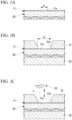
- Figs. 1A to 1D are explanatory views of the welding method not covered by the scope of the present invention, and show a cross section along the up-down direction.
- the first metal member 11 is superimposed on the upper surface of the second metal member 20 (preparation step).
- a hole 11a is formed in the first metal member 11 in advance.
- the shape of the hole 11a is preferably circular or substantially circular.
- the inner diameter (diameter) of the hole 11a is represented as a hole diameter D1.
- the hole diameter D1 is, for example, about 0.5 mm.
- the first metal member 11 and the second metal member 20 are fixed by jigs 31 and 32 (fixing step). More specifically, the first metal member 11 and the second metal member 20 are vertically sandwiched between the upper jig 31 and the lower jig 32.
- a jig hole 31a is formed in the upper jig 31.
- the inner diameter (diameter) of the jig hole 31a is represented as a jig hole diameter D2.
- the jig hole diameter D2 is, for example, 1 mm, and is larger than the hole diameter D1.
- the position of the upper jig 31 with respect to the first metal member 11 is determined such that the center of the jig hole 31a and the center of the hole 11a substantially match in plan view. Since the upper jig 31 and the lower jig 32 sandwich the first metal member 11 and the second metal member 20 with a predetermined pressure, the relative positions of the members are fixed.
- the laser light L is emitted downward from a laser apparatus 33 for welding and is applied near the hole 11a (irradiation step).
- the laser light L is applied to the first metal member 11 or the second metal member 20 through the jig hole 31a of the upper jig 31.
- the irradiation position of the laser light L moves so as to trace a predetermined trajectory T as shown in Fig. 2 .
- Fig. 2 is a view taken in the direction of arrow II in Fig. 1C .
- the dashed line in Fig. 2 indicates the trajectory T of the laser light L.
- the trajectory T in the present embodiment has a spiral shape substantially concentric with the hole 11a, starting at a first point X1 located radially outside the hole 11a and ending at a second point X2 located radially inside the hole 11a.
- the pitch of the spiral trajectory T is referred to as a pitch P.
- the distance between the central axis C of the hole 11a and the first point X1 is represented as an outer radius R1
- the distance between the central axis C and the second point X2 is represented as an inner radius R2.
- the trajectory T can be said to be substantially annular with an inner diameter of 2 ⁇ R2 and an outer diameter of 2 ⁇ R1.
- the hole diameter D1, the jig hole diameter D2, the outer radius R1, and the inner radius R2 are set so as to satisfy the following mathematical expression (1). 0 ⁇ R 2 ⁇ D 1 ⁇ 2 ⁇ R 1 ⁇ D 2 ⁇ 2
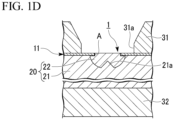
- the first metal member 11 and the second metal member 20 are partially melted.
- an interface between the non-melted portion 21 and the nugget portion (melted portion) 22 appears in the second metal member 20.
- An eutectic portion A is formed at the interface between the first metal member 11 and the second metal member 20.
- the non-melted portion 21 is a portion of the second metal member 20 that is not melted by the heat of the laser light L.
- the nugget portion 22 is a portion of the second metal member 20 that has been melted by the heat of the laser light L and then solidified again.
- the eutectic portion A is a portion where the first metal member 11 and the second metal member 20 are melted and mixed, and solidified in the eutectic state.
- the shapes of the non-melted portion 21, the nugget portion 22, and the eutectic portion A can be checked, for example, by cutting the portion or performing X-ray photography, after welding.
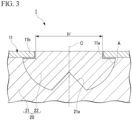
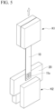
- Fig. 3 is an enlarged view around the nugget portion 22 in Fig. 1D .
- the interface between the nugget portion 22 and the non-melted portion 21 includes a protruding interface 21a that is convex upward.
- the protruding interface 21a is located at a radially central portion of the nugget portion 22. This is because the trajectory T of the laser light L is substantially annular in a top view, as described above. More specifically, since the laser light L is not applied near the central axis C in Fig. 2 , the portion closer to the central axis C of the second metal member 20 is not heated and is not melted. In addition, since the laser light L is applied from above, the lower part of the second metal member 20 does not receive transmitted heat and is not melted. Therefore, a protruding interface 21a as shown in Fig. 3 is formed.
- the bonding strength between the first metal member 11 and the second metal member 20 can be further increased.
- a part of the nugget portion 22 is exposed through the hole 11a. Further, the nugget portion 22 partially enters below the first metal member 11. In other words, the peripheral portion of the hole 11a in the first metal member 11 covers the nugget portion 22 from above. In the present embodiment, a portion of the first metal member 11 that covers the nugget portion 22 is called an overlap portion 11b.
- the reason why the overlap portion 11b is formed is that the melting point of the first metal member 11 is higher than the melting point of the second metal member 20. More specifically, as shown in Fig. 2 , when the first metal member 11 is irradiated with the laser light L, the temperature of the first metal member 11 rises, and the heat is transmitted to raise the temperature of the second metal member 20.
- the second metal member 20 having a lower melting point melts faster than the first metal member 11, the second metal member 20 located below the first metal member 11 remains liquid while the first metal member 11 remains solid.
- the overlap portion 11b covers the nugget portion 22.
- the area of the interface where the first metal member 11 and the second metal member 20 are welded increases, and the welding strength can be further increased.
- the inner diameter of the hole 11a after welding (hereinafter, referred to as a hole diameter D1' after welding) is larger than the hole diameter D1.
- a hole diameter D1' after welding is larger than the hole diameter D1.
- the eutectic portion A is formed over the inner peripheral surface of the hole 11a and the lower surface of the overlap portion 11b.
- the eutectic portion A is preferably thin because it is brittle and has low strength.
- the thickness of the eutectic portion A can be easily controlled by adjusting the dimensions P, R1, R2, D1, or the like.
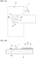
- the welding structure 1 of the present embodiment can be applied to a wiring board 2 with a metal piece as shown in Figs. 4A and 4B , for example.
- the wiring board 2 with a metal piece includes a flexible printed circuit (FPC) 10 and a metal piece (second metal member) 20.
- the flexible printed circuit 10 includes a wiring pattern (first metal member) 11, a base 13 and a coverlay 12 sandwiching the wiring pattern 11.
- the coverlay 12 and the base 13 are provided with rectangular openings 12a and 13a, respectively.
- the wiring pattern 11 is exposed through these openings 12a and 13a.
- a plurality of holes 11a are formed in the portion of the wiring pattern 11 that is exposed through the openings 12a and 13a. The exposed portion is bent downward and superimposed on the upper surface of the metal piece 20 through the opening 13a of the base 13.
- the wiring pattern 11 and the metal piece 20 are partially superimposed, and the wiring pattern 11 and the metal piece 20 are welded by using the bonding method shown in Figs. 1A to 1D , and these can be electrically connected. Further, by performing welding around each of the plurality of holes 11a, the bonding strength can be increased and the electric resistance can be reduced.
- the wiring board 2 with a metal piece as shown in Fig. 4A is manufactured by using the bonding method shown in Figs. 1A to 1D .
- the hole 11a is not formed in the first metal member (wiring pattern) 11 before welding.
- “Without holes” in Table 1 below indicates a sample in which the hole 11a is not formed before welding.
- “With holes” in Table 1 below indicates a sample in which holes 11a are formed before welding.
- the trajectory T of the laser light L is formed in a spiral shape as shown in Fig. 2 .
- the starting point of the trajectory T is a first point X1 located radially outside the hole 11a, and the ending point is a second point X2 located radially inside the hole 11a. That is, the trajectory T has a spiral shape from the outside to the inside of the hole 11a.
- the trajectory T of the laser light L has a pitch P of 0.04 mm, an outer radius R1 of 0.375 mm, and an inner radius R2 of 0.155 mm.
- the laser apparatus 33 uses a fiber laser having a maximum output of 300 W.
- a galvano scanner is used for movement to trace the trajectory T.
- the laser output in Table 1 shows the ratio to the maximum output, and is set to 70% to 80% in the present example.
- the scanning speed when the laser light L traces the trajectory T is 600 mm/s.
- the jig hole diameter D2 is 1 mm.
- the first metal member 11 is a copper foil having a thickness of 0.035 mm.
- a total of ten holes 11a arranged as shown in Fig. 4A are formed in the first metal member 11.
- Each hole diameter D1 is 0.5 mm.
- the second metal member 20 is an aluminum plate (A1050) having a thickness of 1 mm. Note that the conditions for the sample "without holes” are the same as the conditions for the sample "with holes", except that the hole 11a is not formed.
- the hole diameter D1' after welding (see Fig. 3 ) of the sample with holes is 0.85 to 0.9 mm.
- Resistance value shown in Table 1 is a result of measuring the electric resistance between points P1 and P2 shown in Fig. 4A for each sample.
- the interval between the points P1 and P2 is 10 mm.
- the sample without holes has an average resistance value of 0.35 m ⁇ , and the sample with holes has an average resistance value of 0.23 m ⁇ .
- the electric resistance can be reduced by about 34% by forming the hole 11a in advance.
- “Bonding strength” shown in Table 1 is a result of measuring the bonding strength of each sample using a tensile tester as shown in Fig. 5 . More specifically, the flexible printed circuit 10 is clamped by the first clamp K1, and the metal piece 20 is clamped by the second clamp K2. Then, the maximum value of the tensile force when the first clamp K1 and the second clamp K2 are separated at a speed of 10 mm/min is recorded as the bonding strength.
- the sample without holes has an average bonding strength of 2.76 kgf, and the sample with holes has an average bonding strength of 3.47 kgf.
- the bonding strength can be improved by about 26%. This is because the welding structure shown in Fig. 3 is obtained by forming the hole 11a in advance, and separation (peeling) is less likely to occur between the first metal member 11 and the second metal member 20 or between the nugget portion 22 and the non-melted portion 21.
- the welding method not covered by the scope of the present invention includes the preparation step of superimposing the first metal member 11 having the hole 11a formed thereon on the upper surface of the second metal member 20, and the irradiation step of applying laser light L near the hole 11a from above to weld the first metal member 11 and the second metal member 20. Then, in a top view, the trajectory T of the laser light L in the irradiation step is annular from the first point X1 located outside the hole 11a to the second point X2 located inside the hole 11a (across the hole 11a). Thereby, the welding structure 1 as shown in Fig. 3 is obtained.
- the peripheral portion of the hole 11a covers the nugget portion 22 of the second metal member 20.
- the area of the interface where the first metal member 11 and the second metal member 20 are bonded increases, and the bonding strength can be improved. Further, as shown in the example, the electric resistance between the first metal member 11 and the second metal member 20 can be reduced.
- the interface between the nugget portion 22 and the non-melted portion 21 in the second metal member 20 includes a protruding interface 21a that protrudes upward.
- the occurrence of separation (peeling) between the non-melted portion 21 and the nugget portion 22 is suppressed, and the bonding strength can be more reliably increased.
- the second metal member 20 melts faster than the first metal member 11, so that the overlap portion 11b of the first metal member 11 is easily formed.
- the thickness of the eutectic portion A can be easily controlled by adjusting the welding parameters P, R1, R2, D1, or the like, because the trajectory T of the laser light L is spiral in a top view.
- the welding structure 1 as described above to the wiring board 2 with a metal piece, the bonding strength between the wiring pattern 11 and the metal piece 20 is increased, and the electric resistance between the wiring pattern 11 and the metal piece 20 can be reduced.
- the welding method and the welding structure 1 of the above embodiment may be used for applications other than the wiring board 2 with a metal piece.
- trajectory T of the laser light L may be directed from the radial inside (the second point X2) of the hole 11a to the radial outside (the first point X1).
- trajectory T may be substantially annular as a whole, for example, by making the trajectory radial about the central axis C.
Landscapes
- Engineering & Computer Science (AREA)
- Physics & Mathematics (AREA)
- Optics & Photonics (AREA)
- Plasma & Fusion (AREA)
- Mechanical Engineering (AREA)
- Manufacturing & Machinery (AREA)
- Microelectronics & Electronic Packaging (AREA)
- Laser Beam Processing (AREA)
- Connections Effected By Soldering, Adhesion, Or Permanent Deformation (AREA)
- Coupling Device And Connection With Printed Circuit (AREA)
Applications Claiming Priority (2)
| Application Number | Priority Date | Filing Date | Title |
|---|---|---|---|
| JP2017253541 | 2017-12-28 | ||
| PCT/JP2018/048031 WO2019131828A1 (ja) | 2017-12-28 | 2018-12-27 | 溶接構造、金属片付き配線基板、および溶接方法 |
Publications (3)
| Publication Number | Publication Date |
|---|---|
| EP3733339A1 EP3733339A1 (en) | 2020-11-04 |
| EP3733339A4 EP3733339A4 (en) | 2021-11-17 |
| EP3733339B1 true EP3733339B1 (en) | 2024-02-07 |
Family
ID=67063789
Family Applications (1)
| Application Number | Title | Priority Date | Filing Date |
|---|---|---|---|
| EP18895465.5A Active EP3733339B1 (en) | 2017-12-28 | 2018-12-27 | Welding structure, wiring board with metal piece |
Country Status (5)
| Country | Link |
|---|---|
| US (1) | US11597038B2 (ja) |
| EP (1) | EP3733339B1 (ja) |
| JP (1) | JP6896889B2 (ja) |
| CN (2) | CN113618237B (ja) |
| WO (1) | WO2019131828A1 (ja) |
Families Citing this family (5)
| Publication number | Priority date | Publication date | Assignee | Title |
|---|---|---|---|---|
| WO2021111966A1 (ja) * | 2019-12-05 | 2021-06-10 | 株式会社フジクラ | 金属片付き配線基板 |
| CN114346601B (zh) * | 2021-12-28 | 2023-01-31 | 富联裕展科技(深圳)有限公司 | 复合材料结构以及复合材料结构的加工方法 |
| WO2023234689A1 (ko) * | 2022-05-31 | 2023-12-07 | 주식회사 엘지에너지솔루션 | 레이저 용접장치 및 이를 이용한 용접방법 |
| WO2024063255A1 (ko) * | 2022-09-23 | 2024-03-28 | 삼성전자주식회사 | 하우징과 연결된 안테나 구조를 포함하는 전자 장치 |
| CN118616910B (zh) * | 2024-08-09 | 2024-10-25 | 北京金橙子科技股份有限公司 | 一种对环形图案的交叉填充方法及存储介质 |
Family Cites Families (21)
| Publication number | Priority date | Publication date | Assignee | Title |
|---|---|---|---|---|
| JPS6057430B2 (ja) * | 1980-11-29 | 1985-12-14 | 松下電工株式会社 | レ−ザビ−ムによる溶接方法 |
| US5306891A (en) * | 1992-04-02 | 1994-04-26 | Motorola, Inc. | Laser welding process for attaching metal to ceramic substrate |
| JPH08332582A (ja) * | 1995-06-05 | 1996-12-17 | Toshiba Corp | レーザ溶接方法 |
| JPH10334956A (ja) | 1997-05-28 | 1998-12-18 | Harness Sogo Gijutsu Kenkyusho:Kk | レーザ溶接構造 |
| JP3343066B2 (ja) * | 1997-11-04 | 2002-11-11 | 株式会社オートネットワーク技術研究所 | バスバーのレーザ溶接構造 |
| JP2005123419A (ja) * | 2003-10-17 | 2005-05-12 | Tohoku Pioneer Corp | 配線基板、配線パターンの形成方法、有機elパネル |
| JP2005347143A (ja) * | 2004-06-04 | 2005-12-15 | Fujikura Ltd | コネクタ |
| JP2007265962A (ja) * | 2006-02-28 | 2007-10-11 | Hitachi Ltd | レーザ溶接方法,コントロールユニットの製造方法、及び車両用コントロールユニット |
| JP5118862B2 (ja) * | 2007-03-05 | 2013-01-16 | トヨタ自動車株式会社 | レーザ接合方法 |
| JP5248344B2 (ja) * | 2009-01-20 | 2013-07-31 | 本田技研工業株式会社 | レーザ溶接方法 |
| WO2012164839A1 (ja) * | 2011-05-30 | 2012-12-06 | パナソニック株式会社 | レーザ接合部品およびその製造方法 |
| JP5932323B2 (ja) * | 2011-12-19 | 2016-06-08 | 株式会社東芝 | 二次電池及び二次電池の製造方法 |
| CN102896398A (zh) * | 2012-10-10 | 2013-01-30 | 上海交通大学 | 基于cmt的铝合金电弧点焊方法及焊接系统 |
| WO2014123022A1 (ja) | 2013-02-05 | 2014-08-14 | 株式会社日立製作所 | レーザ接合装置及びレーザ接合方法 |
| CN105358282B (zh) * | 2013-07-31 | 2017-10-13 | 新日铁住金株式会社 | 电弧点焊接头及其制造方法 |
| US10155285B2 (en) * | 2014-01-10 | 2018-12-18 | Panasonic Intellectual Property Management Co., Ltd. | Laser welding method and laser welding device |
| CN106029291B (zh) | 2014-02-25 | 2018-05-04 | 松下知识产权经营株式会社 | 激光焊接方法 |
| CN105855706B (zh) * | 2015-02-09 | 2018-02-13 | 司浦爱激光技术英国有限公司 | 激光焊缝 |
| GB201502149D0 (en) * | 2015-02-09 | 2015-03-25 | Spi Lasers Uk Ltd | Apparatus and method for laser welding |
| JP6149887B2 (ja) * | 2015-04-03 | 2017-06-21 | トヨタ自動車株式会社 | 溶接方法 |
| US10118249B2 (en) * | 2015-10-15 | 2018-11-06 | GM Global Technology Operations LLC | Laser beam welding with a spiral weld path having a first order of continuity |
-
2018
- 2018-12-27 EP EP18895465.5A patent/EP3733339B1/en active Active
- 2018-12-27 US US16/650,726 patent/US11597038B2/en active Active
- 2018-12-27 JP JP2019562141A patent/JP6896889B2/ja active Active
- 2018-12-27 CN CN202110880212.3A patent/CN113618237B/zh active Active
- 2018-12-27 WO PCT/JP2018/048031 patent/WO2019131828A1/ja not_active Ceased
- 2018-12-27 CN CN201880061937.6A patent/CN111163896B/zh active Active
Also Published As
| Publication number | Publication date |
|---|---|
| US20200306882A1 (en) | 2020-10-01 |
| CN111163896A (zh) | 2020-05-15 |
| JPWO2019131828A1 (ja) | 2020-11-19 |
| WO2019131828A1 (ja) | 2019-07-04 |
| EP3733339A1 (en) | 2020-11-04 |
| CN113618237A (zh) | 2021-11-09 |
| CN111163896B (zh) | 2022-10-04 |
| JP6896889B2 (ja) | 2021-06-30 |
| CN113618237B (zh) | 2023-09-22 |
| EP3733339A4 (en) | 2021-11-17 |
| US11597038B2 (en) | 2023-03-07 |
Similar Documents
| Publication | Publication Date | Title |
|---|---|---|
| EP3733339B1 (en) | Welding structure, wiring board with metal piece | |
| KR960006711B1 (ko) | 반도체장치용 리이드프레임의 제조방법과 반도체장치용 리이드프레임 및 수지봉지형 반도체장치 | |
| KR101493205B1 (ko) | 압착 단자의 제조 방법, 압착 단자 및 와이어 하네스 | |
| US5144535A (en) | Method of mounting electrical and/or electronic components of a printed circuit board | |
| CN108883484B (zh) | 接合结构 | |
| US4628150A (en) | Bonding and bonded products | |
| EP2684637A1 (en) | Laser welding component and method for manufacturing same | |
| JP7110907B2 (ja) | 異種金属部材の重ね溶接方法 | |
| JP2012004281A (ja) | レーザ溶接方法、電子部品接続構造及びレーザ溶接検査方法 | |
| CN112351855A (zh) | 镀敷钢板的接合方法以及接合构造体 | |
| US10421153B2 (en) | Laser welding method and laser welding device | |
| JP3296070B2 (ja) | 接合構造体及びその製造方法 | |
| JP5931100B2 (ja) | 端子製造装置 | |
| JP4961531B2 (ja) | 異種金属の接合方法及び接合構造 | |
| CN111819026B (zh) | 接合结构以及接合方法 | |
| KR101060135B1 (ko) | 용접 방법 | |
| US20190269020A1 (en) | System and method for connecting flat flexible cable to printed circuit board | |
| EP2144284A1 (de) | Verfahren zum Herstellen eines Anschlusskontaktes an einem Halbleiterbauelement für die Leistungselektronik und elektronisches Bauteil mit einem auf diese Weise an einem Halblei-terbauelement hergestellten Anschlusskontakt | |
| JP7546208B2 (ja) | 接合構造 | |
| EP2145716A1 (en) | Welding method and welding structure of conductive terminals | |
| JP2012016741A (ja) | レーザ隅肉溶接方法 | |
| EP2285197A1 (de) | Verfahren zur Verbindung eines elektronischen Bauteils mit einer Leiterplatte | |
| JPS60210383A (ja) | 細線接合方法 | |
| CN114555279B (zh) | 焊接方法及焊接结构 | |
| JP2005274560A (ja) | 放射線検出器用フィルタの実装方法 |
Legal Events
| Date | Code | Title | Description |
|---|---|---|---|
| STAA | Information on the status of an ep patent application or granted ep patent |
Free format text: STATUS: THE INTERNATIONAL PUBLICATION HAS BEEN MADE |
|
| PUAI | Public reference made under article 153(3) epc to a published international application that has entered the european phase |
Free format text: ORIGINAL CODE: 0009012 |
|
| STAA | Information on the status of an ep patent application or granted ep patent |
Free format text: STATUS: REQUEST FOR EXAMINATION WAS MADE |
|
| 17P | Request for examination filed |
Effective date: 20200323 |
|
| AK | Designated contracting states |
Kind code of ref document: A1 Designated state(s): AL AT BE BG CH CY CZ DE DK EE ES FI FR GB GR HR HU IE IS IT LI LT LU LV MC MK MT NL NO PL PT RO RS SE SI SK SM TR |
|
| AX | Request for extension of the european patent |
Extension state: BA ME |
|
| DAV | Request for validation of the european patent (deleted) | ||
| DAX | Request for extension of the european patent (deleted) | ||
| A4 | Supplementary search report drawn up and despatched |
Effective date: 20211014 |
|
| RIC1 | Information provided on ipc code assigned before grant |
Ipc: B23K 103/12 20060101ALN20211008BHEP Ipc: B23K 103/10 20060101ALN20211008BHEP Ipc: B23K 101/42 20060101ALN20211008BHEP Ipc: H05K 3/32 20060101ALI20211008BHEP Ipc: H05K 1/11 20060101ALI20211008BHEP Ipc: H01R 43/02 20060101ALI20211008BHEP Ipc: H01R 12/62 20110101ALI20211008BHEP Ipc: H01R 4/02 20060101ALI20211008BHEP Ipc: B23K 26/323 20140101ALI20211008BHEP Ipc: B23K 26/244 20140101ALI20211008BHEP Ipc: B23K 26/24 20140101AFI20211008BHEP |
|
| STAA | Information on the status of an ep patent application or granted ep patent |
Free format text: STATUS: EXAMINATION IS IN PROGRESS |
|
| 17Q | First examination report despatched |
Effective date: 20220920 |
|
| REG | Reference to a national code |
Ref country code: DE Ref legal event code: R079 Free format text: PREVIOUS MAIN CLASS: B23K0026210000 Ipc: B23K0026240000 Ref country code: DE Ref legal event code: R079 Ref document number: 602018065077 Country of ref document: DE Free format text: PREVIOUS MAIN CLASS: B23K0026210000 Ipc: B23K0026240000 |
|
| GRAP | Despatch of communication of intention to grant a patent |
Free format text: ORIGINAL CODE: EPIDOSNIGR1 |
|
| STAA | Information on the status of an ep patent application or granted ep patent |
Free format text: STATUS: GRANT OF PATENT IS INTENDED |
|
| RIC1 | Information provided on ipc code assigned before grant |
Ipc: B23K 103/12 20060101ALN20230713BHEP Ipc: B23K 103/10 20060101ALN20230713BHEP Ipc: B23K 101/42 20060101ALN20230713BHEP Ipc: H05K 3/32 20060101ALI20230713BHEP Ipc: H05K 1/11 20060101ALI20230713BHEP Ipc: H01R 43/02 20060101ALI20230713BHEP Ipc: H01R 12/62 20110101ALI20230713BHEP Ipc: H01R 4/02 20060101ALI20230713BHEP Ipc: B23K 26/323 20140101ALI20230713BHEP Ipc: B23K 26/244 20140101ALI20230713BHEP Ipc: B23K 26/24 20140101AFI20230713BHEP |
|
| RIC1 | Information provided on ipc code assigned before grant |
Ipc: B23K 103/12 20060101ALN20230718BHEP Ipc: B23K 103/10 20060101ALN20230718BHEP Ipc: B23K 101/42 20060101ALN20230718BHEP Ipc: H05K 3/32 20060101ALI20230718BHEP Ipc: H05K 1/11 20060101ALI20230718BHEP Ipc: H01R 43/02 20060101ALI20230718BHEP Ipc: H01R 12/62 20110101ALI20230718BHEP Ipc: H01R 4/02 20060101ALI20230718BHEP Ipc: B23K 26/323 20140101ALI20230718BHEP Ipc: B23K 26/244 20140101ALI20230718BHEP Ipc: B23K 26/24 20140101AFI20230718BHEP |
|
| INTG | Intention to grant announced |
Effective date: 20230808 |
|
| RIC1 | Information provided on ipc code assigned before grant |
Ipc: B23K 103/12 20060101ALN20230731BHEP Ipc: B23K 103/10 20060101ALN20230731BHEP Ipc: B23K 101/42 20060101ALN20230731BHEP Ipc: H05K 3/32 20060101ALI20230731BHEP Ipc: H05K 1/11 20060101ALI20230731BHEP Ipc: H01R 43/02 20060101ALI20230731BHEP Ipc: H01R 12/62 20110101ALI20230731BHEP Ipc: H01R 4/02 20060101ALI20230731BHEP Ipc: B23K 26/323 20140101ALI20230731BHEP Ipc: B23K 26/244 20140101ALI20230731BHEP Ipc: B23K 26/24 20140101AFI20230731BHEP |
|
| GRAS | Grant fee paid |
Free format text: ORIGINAL CODE: EPIDOSNIGR3 |
|
| GRAA | (expected) grant |
Free format text: ORIGINAL CODE: 0009210 |
|
| STAA | Information on the status of an ep patent application or granted ep patent |
Free format text: STATUS: THE PATENT HAS BEEN GRANTED |
|
| AK | Designated contracting states |
Kind code of ref document: B1 Designated state(s): AL AT BE BG CH CY CZ DE DK EE ES FI FR GB GR HR HU IE IS IT LI LT LU LV MC MK MT NL NO PL PT RO RS SE SI SK SM TR |
|
| REG | Reference to a national code |
Ref country code: GB Ref legal event code: FG4D |
|
| REG | Reference to a national code |
Ref country code: CH Ref legal event code: EP |
|
| REG | Reference to a national code |
Ref country code: IE Ref legal event code: FG4D |
|
| REG | Reference to a national code |
Ref country code: DE Ref legal event code: R096 Ref document number: 602018065077 Country of ref document: DE |
|
| REG | Reference to a national code |
Ref country code: LT Ref legal event code: MG9D |
|
| REG | Reference to a national code |
Ref country code: NL Ref legal event code: MP Effective date: 20240207 |
|
| PG25 | Lapsed in a contracting state [announced via postgrant information from national office to epo] |
Ref country code: IS Free format text: LAPSE BECAUSE OF FAILURE TO SUBMIT A TRANSLATION OF THE DESCRIPTION OR TO PAY THE FEE WITHIN THE PRESCRIBED TIME-LIMIT Effective date: 20240607 |
|
| PG25 | Lapsed in a contracting state [announced via postgrant information from national office to epo] |
Ref country code: LT Free format text: LAPSE BECAUSE OF FAILURE TO SUBMIT A TRANSLATION OF THE DESCRIPTION OR TO PAY THE FEE WITHIN THE PRESCRIBED TIME-LIMIT Effective date: 20240207 |
|
| PG25 | Lapsed in a contracting state [announced via postgrant information from national office to epo] |
Ref country code: GR Free format text: LAPSE BECAUSE OF FAILURE TO SUBMIT A TRANSLATION OF THE DESCRIPTION OR TO PAY THE FEE WITHIN THE PRESCRIBED TIME-LIMIT Effective date: 20240508 |
|
| REG | Reference to a national code |
Ref country code: AT Ref legal event code: MK05 Ref document number: 1655064 Country of ref document: AT Kind code of ref document: T Effective date: 20240207 |
|
| PG25 | Lapsed in a contracting state [announced via postgrant information from national office to epo] |
Ref country code: RS Free format text: LAPSE BECAUSE OF FAILURE TO SUBMIT A TRANSLATION OF THE DESCRIPTION OR TO PAY THE FEE WITHIN THE PRESCRIBED TIME-LIMIT Effective date: 20240507 Ref country code: NL Free format text: LAPSE BECAUSE OF FAILURE TO SUBMIT A TRANSLATION OF THE DESCRIPTION OR TO PAY THE FEE WITHIN THE PRESCRIBED TIME-LIMIT Effective date: 20240207 Ref country code: HR Free format text: LAPSE BECAUSE OF FAILURE TO SUBMIT A TRANSLATION OF THE DESCRIPTION OR TO PAY THE FEE WITHIN THE PRESCRIBED TIME-LIMIT Effective date: 20240207 |
|
| PG25 | Lapsed in a contracting state [announced via postgrant information from national office to epo] |
Ref country code: ES Free format text: LAPSE BECAUSE OF FAILURE TO SUBMIT A TRANSLATION OF THE DESCRIPTION OR TO PAY THE FEE WITHIN THE PRESCRIBED TIME-LIMIT Effective date: 20240207 |
|
| PG25 | Lapsed in a contracting state [announced via postgrant information from national office to epo] |
Ref country code: AT Free format text: LAPSE BECAUSE OF FAILURE TO SUBMIT A TRANSLATION OF THE DESCRIPTION OR TO PAY THE FEE WITHIN THE PRESCRIBED TIME-LIMIT Effective date: 20240207 |
|
| PG25 | Lapsed in a contracting state [announced via postgrant information from national office to epo] |
Ref country code: RS Free format text: LAPSE BECAUSE OF FAILURE TO SUBMIT A TRANSLATION OF THE DESCRIPTION OR TO PAY THE FEE WITHIN THE PRESCRIBED TIME-LIMIT Effective date: 20240507 Ref country code: NO Free format text: LAPSE BECAUSE OF FAILURE TO SUBMIT A TRANSLATION OF THE DESCRIPTION OR TO PAY THE FEE WITHIN THE PRESCRIBED TIME-LIMIT Effective date: 20240507 Ref country code: NL Free format text: LAPSE BECAUSE OF FAILURE TO SUBMIT A TRANSLATION OF THE DESCRIPTION OR TO PAY THE FEE WITHIN THE PRESCRIBED TIME-LIMIT Effective date: 20240207 Ref country code: LT Free format text: LAPSE BECAUSE OF FAILURE TO SUBMIT A TRANSLATION OF THE DESCRIPTION OR TO PAY THE FEE WITHIN THE PRESCRIBED TIME-LIMIT Effective date: 20240207 Ref country code: IS Free format text: LAPSE BECAUSE OF FAILURE TO SUBMIT A TRANSLATION OF THE DESCRIPTION OR TO PAY THE FEE WITHIN THE PRESCRIBED TIME-LIMIT Effective date: 20240607 Ref country code: HR Free format text: LAPSE BECAUSE OF FAILURE TO SUBMIT A TRANSLATION OF THE DESCRIPTION OR TO PAY THE FEE WITHIN THE PRESCRIBED TIME-LIMIT Effective date: 20240207 Ref country code: GR Free format text: LAPSE BECAUSE OF FAILURE TO SUBMIT A TRANSLATION OF THE DESCRIPTION OR TO PAY THE FEE WITHIN THE PRESCRIBED TIME-LIMIT Effective date: 20240508 Ref country code: FI Free format text: LAPSE BECAUSE OF FAILURE TO SUBMIT A TRANSLATION OF THE DESCRIPTION OR TO PAY THE FEE WITHIN THE PRESCRIBED TIME-LIMIT Effective date: 20240207 Ref country code: ES Free format text: LAPSE BECAUSE OF FAILURE TO SUBMIT A TRANSLATION OF THE DESCRIPTION OR TO PAY THE FEE WITHIN THE PRESCRIBED TIME-LIMIT Effective date: 20240207 Ref country code: BG Free format text: LAPSE BECAUSE OF FAILURE TO SUBMIT A TRANSLATION OF THE DESCRIPTION OR TO PAY THE FEE WITHIN THE PRESCRIBED TIME-LIMIT Effective date: 20240207 Ref country code: AT Free format text: LAPSE BECAUSE OF FAILURE TO SUBMIT A TRANSLATION OF THE DESCRIPTION OR TO PAY THE FEE WITHIN THE PRESCRIBED TIME-LIMIT Effective date: 20240207 |
|
| PG25 | Lapsed in a contracting state [announced via postgrant information from national office to epo] |
Ref country code: PL Free format text: LAPSE BECAUSE OF FAILURE TO SUBMIT A TRANSLATION OF THE DESCRIPTION OR TO PAY THE FEE WITHIN THE PRESCRIBED TIME-LIMIT Effective date: 20240207 Ref country code: PT Free format text: LAPSE BECAUSE OF FAILURE TO SUBMIT A TRANSLATION OF THE DESCRIPTION OR TO PAY THE FEE WITHIN THE PRESCRIBED TIME-LIMIT Effective date: 20240607 |
|
| PG25 | Lapsed in a contracting state [announced via postgrant information from national office to epo] |
Ref country code: SE Free format text: LAPSE BECAUSE OF FAILURE TO SUBMIT A TRANSLATION OF THE DESCRIPTION OR TO PAY THE FEE WITHIN THE PRESCRIBED TIME-LIMIT Effective date: 20240207 Ref country code: PT Free format text: LAPSE BECAUSE OF FAILURE TO SUBMIT A TRANSLATION OF THE DESCRIPTION OR TO PAY THE FEE WITHIN THE PRESCRIBED TIME-LIMIT Effective date: 20240607 Ref country code: PL Free format text: LAPSE BECAUSE OF FAILURE TO SUBMIT A TRANSLATION OF THE DESCRIPTION OR TO PAY THE FEE WITHIN THE PRESCRIBED TIME-LIMIT Effective date: 20240207 Ref country code: LV Free format text: LAPSE BECAUSE OF FAILURE TO SUBMIT A TRANSLATION OF THE DESCRIPTION OR TO PAY THE FEE WITHIN THE PRESCRIBED TIME-LIMIT Effective date: 20240207 |
|
| PG25 | Lapsed in a contracting state [announced via postgrant information from national office to epo] |
Ref country code: DK Free format text: LAPSE BECAUSE OF FAILURE TO SUBMIT A TRANSLATION OF THE DESCRIPTION OR TO PAY THE FEE WITHIN THE PRESCRIBED TIME-LIMIT Effective date: 20240207 |
|
| PG25 | Lapsed in a contracting state [announced via postgrant information from national office to epo] |
Ref country code: SM Free format text: LAPSE BECAUSE OF FAILURE TO SUBMIT A TRANSLATION OF THE DESCRIPTION OR TO PAY THE FEE WITHIN THE PRESCRIBED TIME-LIMIT Effective date: 20240207 |
|
| PG25 | Lapsed in a contracting state [announced via postgrant information from national office to epo] |
Ref country code: CZ Free format text: LAPSE BECAUSE OF FAILURE TO SUBMIT A TRANSLATION OF THE DESCRIPTION OR TO PAY THE FEE WITHIN THE PRESCRIBED TIME-LIMIT Effective date: 20240207 Ref country code: EE Free format text: LAPSE BECAUSE OF FAILURE TO SUBMIT A TRANSLATION OF THE DESCRIPTION OR TO PAY THE FEE WITHIN THE PRESCRIBED TIME-LIMIT Effective date: 20240207 |
|
| PG25 | Lapsed in a contracting state [announced via postgrant information from national office to epo] |
Ref country code: SK Free format text: LAPSE BECAUSE OF FAILURE TO SUBMIT A TRANSLATION OF THE DESCRIPTION OR TO PAY THE FEE WITHIN THE PRESCRIBED TIME-LIMIT Effective date: 20240207 |
|
| PG25 | Lapsed in a contracting state [announced via postgrant information from national office to epo] |
Ref country code: SM Free format text: LAPSE BECAUSE OF FAILURE TO SUBMIT A TRANSLATION OF THE DESCRIPTION OR TO PAY THE FEE WITHIN THE PRESCRIBED TIME-LIMIT Effective date: 20240207 Ref country code: SK Free format text: LAPSE BECAUSE OF FAILURE TO SUBMIT A TRANSLATION OF THE DESCRIPTION OR TO PAY THE FEE WITHIN THE PRESCRIBED TIME-LIMIT Effective date: 20240207 Ref country code: RO Free format text: LAPSE BECAUSE OF FAILURE TO SUBMIT A TRANSLATION OF THE DESCRIPTION OR TO PAY THE FEE WITHIN THE PRESCRIBED TIME-LIMIT Effective date: 20240207 Ref country code: EE Free format text: LAPSE BECAUSE OF FAILURE TO SUBMIT A TRANSLATION OF THE DESCRIPTION OR TO PAY THE FEE WITHIN THE PRESCRIBED TIME-LIMIT Effective date: 20240207 Ref country code: DK Free format text: LAPSE BECAUSE OF FAILURE TO SUBMIT A TRANSLATION OF THE DESCRIPTION OR TO PAY THE FEE WITHIN THE PRESCRIBED TIME-LIMIT Effective date: 20240207 Ref country code: CZ Free format text: LAPSE BECAUSE OF FAILURE TO SUBMIT A TRANSLATION OF THE DESCRIPTION OR TO PAY THE FEE WITHIN THE PRESCRIBED TIME-LIMIT Effective date: 20240207 |
|
| REG | Reference to a national code |
Ref country code: DE Ref legal event code: R097 Ref document number: 602018065077 Country of ref document: DE |
|
| PG25 | Lapsed in a contracting state [announced via postgrant information from national office to epo] |
Ref country code: IT Free format text: LAPSE BECAUSE OF FAILURE TO SUBMIT A TRANSLATION OF THE DESCRIPTION OR TO PAY THE FEE WITHIN THE PRESCRIBED TIME-LIMIT Effective date: 20240207 |
|
| PLBE | No opposition filed within time limit |
Free format text: ORIGINAL CODE: 0009261 |
|
| STAA | Information on the status of an ep patent application or granted ep patent |
Free format text: STATUS: NO OPPOSITION FILED WITHIN TIME LIMIT |
|
| PG25 | Lapsed in a contracting state [announced via postgrant information from national office to epo] |
Ref country code: IT Free format text: LAPSE BECAUSE OF FAILURE TO SUBMIT A TRANSLATION OF THE DESCRIPTION OR TO PAY THE FEE WITHIN THE PRESCRIBED TIME-LIMIT Effective date: 20240207 |
|
| PGFP | Annual fee paid to national office [announced via postgrant information from national office to epo] |
Ref country code: DE Payment date: 20241029 Year of fee payment: 7 |
|
| 26N | No opposition filed |
Effective date: 20241108 |
|
| PGFP | Annual fee paid to national office [announced via postgrant information from national office to epo] |
Ref country code: FR Payment date: 20241111 Year of fee payment: 7 |
|
| PG25 | Lapsed in a contracting state [announced via postgrant information from national office to epo] |
Ref country code: SI Free format text: LAPSE BECAUSE OF FAILURE TO SUBMIT A TRANSLATION OF THE DESCRIPTION OR TO PAY THE FEE WITHIN THE PRESCRIBED TIME-LIMIT Effective date: 20240207 |
|
| PG25 | Lapsed in a contracting state [announced via postgrant information from national office to epo] |
Ref country code: MC Free format text: LAPSE BECAUSE OF FAILURE TO SUBMIT A TRANSLATION OF THE DESCRIPTION OR TO PAY THE FEE WITHIN THE PRESCRIBED TIME-LIMIT Effective date: 20240207 |
|
| REG | Reference to a national code |
Ref country code: CH Ref legal event code: PL |
|
| PG25 | Lapsed in a contracting state [announced via postgrant information from national office to epo] |
Ref country code: LU Free format text: LAPSE BECAUSE OF NON-PAYMENT OF DUE FEES Effective date: 20241227 |
|
| GBPC | Gb: european patent ceased through non-payment of renewal fee |
Effective date: 20241227 |
|
| REG | Reference to a national code |
Ref country code: BE Ref legal event code: MM Effective date: 20241231 |
|
| PG25 | Lapsed in a contracting state [announced via postgrant information from national office to epo] |
Ref country code: GB Free format text: LAPSE BECAUSE OF NON-PAYMENT OF DUE FEES Effective date: 20241227 Ref country code: BE Free format text: LAPSE BECAUSE OF NON-PAYMENT OF DUE FEES Effective date: 20241231 |
|
| PG25 | Lapsed in a contracting state [announced via postgrant information from national office to epo] |
Ref country code: CH Free format text: LAPSE BECAUSE OF NON-PAYMENT OF DUE FEES Effective date: 20241231 |
|
| PG25 | Lapsed in a contracting state [announced via postgrant information from national office to epo] |
Ref country code: IE Free format text: LAPSE BECAUSE OF NON-PAYMENT OF DUE FEES Effective date: 20241227 |