EP3709061A2 - Verfahren und system zur homogenisierung von diodenlaserpumpenanordnungen - Google Patents
Verfahren und system zur homogenisierung von diodenlaserpumpenanordnungen Download PDFInfo
- Publication number
- EP3709061A2 EP3709061A2 EP20160366.9A EP20160366A EP3709061A2 EP 3709061 A2 EP3709061 A2 EP 3709061A2 EP 20160366 A EP20160366 A EP 20160366A EP 3709061 A2 EP3709061 A2 EP 3709061A2
- Authority
- EP
- European Patent Office
- Prior art keywords
- optical element
- diffractive
- ptr glass
- intensity
- transparent optical
- Prior art date
- Legal status (The legal status is an assumption and is not a legal conclusion. Google has not performed a legal analysis and makes no representation as to the accuracy of the status listed.)
- Granted
Links
Images


Classifications
-
- H—ELECTRICITY
- H01—ELECTRIC ELEMENTS
- H01S—DEVICES USING THE PROCESS OF LIGHT AMPLIFICATION BY STIMULATED EMISSION OF RADIATION [LASER] TO AMPLIFY OR GENERATE LIGHT; DEVICES USING STIMULATED EMISSION OF ELECTROMAGNETIC RADIATION IN WAVE RANGES OTHER THAN OPTICAL
- H01S3/00—Lasers, i.e. devices using stimulated emission of electromagnetic radiation in the infrared, visible or ultraviolet wave range
- H01S3/09—Processes or apparatus for excitation, e.g. pumping
- H01S3/091—Processes or apparatus for excitation, e.g. pumping using optical pumping
- H01S3/094—Processes or apparatus for excitation, e.g. pumping using optical pumping by coherent light
- H01S3/094049—Guiding of the pump light
-
- G—PHYSICS
- G02—OPTICS
- G02B—OPTICAL ELEMENTS, SYSTEMS OR APPARATUS
- G02B19/00—Condensers, e.g. light collectors or similar non-imaging optics
- G02B19/0004—Condensers, e.g. light collectors or similar non-imaging optics characterised by the optical means employed
- G02B19/0009—Condensers, e.g. light collectors or similar non-imaging optics characterised by the optical means employed having refractive surfaces only
- G02B19/0014—Condensers, e.g. light collectors or similar non-imaging optics characterised by the optical means employed having refractive surfaces only at least one surface having optical power
-
- G—PHYSICS
- G02—OPTICS
- G02B—OPTICAL ELEMENTS, SYSTEMS OR APPARATUS
- G02B19/00—Condensers, e.g. light collectors or similar non-imaging optics
- G02B19/0033—Condensers, e.g. light collectors or similar non-imaging optics characterised by the use
- G02B19/0047—Condensers, e.g. light collectors or similar non-imaging optics characterised by the use for use with a light source
- G02B19/0052—Condensers, e.g. light collectors or similar non-imaging optics characterised by the use for use with a light source the light source comprising a laser diode
- G02B19/0057—Condensers, e.g. light collectors or similar non-imaging optics characterised by the use for use with a light source the light source comprising a laser diode in the form of a laser diode array, e.g. laser diode bar
-
- G—PHYSICS
- G02—OPTICS
- G02B—OPTICAL ELEMENTS, SYSTEMS OR APPARATUS
- G02B19/00—Condensers, e.g. light collectors or similar non-imaging optics
- G02B19/0033—Condensers, e.g. light collectors or similar non-imaging optics characterised by the use
- G02B19/0095—Condensers, e.g. light collectors or similar non-imaging optics characterised by the use for use with ultraviolet radiation
-
- G—PHYSICS
- G02—OPTICS
- G02B—OPTICAL ELEMENTS, SYSTEMS OR APPARATUS
- G02B27/00—Optical systems or apparatus not provided for by any of the groups G02B1/00 - G02B26/00, G02B30/00
- G02B27/09—Beam shaping, e.g. changing the cross-sectional area, not otherwise provided for
- G02B27/0927—Systems for changing the beam intensity distribution, e.g. Gaussian to top-hat
-
- G—PHYSICS
- G02—OPTICS
- G02B—OPTICAL ELEMENTS, SYSTEMS OR APPARATUS
- G02B27/00—Optical systems or apparatus not provided for by any of the groups G02B1/00 - G02B26/00, G02B30/00
- G02B27/09—Beam shaping, e.g. changing the cross-sectional area, not otherwise provided for
- G02B27/0938—Using specific optical elements
- G02B27/0944—Diffractive optical elements, e.g. gratings, holograms
-
- G—PHYSICS
- G02—OPTICS
- G02B—OPTICAL ELEMENTS, SYSTEMS OR APPARATUS
- G02B5/00—Optical elements other than lenses
- G02B5/18—Diffraction gratings
- G02B5/1847—Manufacturing methods
- G02B5/1857—Manufacturing methods using exposure or etching means, e.g. holography, photolithography, exposure to electron or ion beams
-
- G—PHYSICS
- G02—OPTICS
- G02B—OPTICAL ELEMENTS, SYSTEMS OR APPARATUS
- G02B27/00—Optical systems or apparatus not provided for by any of the groups G02B1/00 - G02B26/00, G02B30/00
- G02B27/09—Beam shaping, e.g. changing the cross-sectional area, not otherwise provided for
- G02B27/0916—Adapting the beam shape of a semiconductor light source such as a laser diode or an LED, e.g. for efficiently coupling into optical fibers
- G02B27/0922—Adapting the beam shape of a semiconductor light source such as a laser diode or an LED, e.g. for efficiently coupling into optical fibers the semiconductor light source comprising an array of light emitters
-
- H—ELECTRICITY
- H01—ELECTRIC ELEMENTS
- H01S—DEVICES USING THE PROCESS OF LIGHT AMPLIFICATION BY STIMULATED EMISSION OF RADIATION [LASER] TO AMPLIFY OR GENERATE LIGHT; DEVICES USING STIMULATED EMISSION OF ELECTROMAGNETIC RADIATION IN WAVE RANGES OTHER THAN OPTICAL
- H01S3/00—Lasers, i.e. devices using stimulated emission of electromagnetic radiation in the infrared, visible or ultraviolet wave range
- H01S3/005—Optical devices external to the laser cavity, specially adapted for lasers, e.g. for homogenisation of the beam or for manipulating laser pulses, e.g. pulse shaping
-
- H—ELECTRICITY
- H01—ELECTRIC ELEMENTS
- H01S—DEVICES USING THE PROCESS OF LIGHT AMPLIFICATION BY STIMULATED EMISSION OF RADIATION [LASER] TO AMPLIFY OR GENERATE LIGHT; DEVICES USING STIMULATED EMISSION OF ELECTROMAGNETIC RADIATION IN WAVE RANGES OTHER THAN OPTICAL
- H01S3/00—Lasers, i.e. devices using stimulated emission of electromagnetic radiation in the infrared, visible or ultraviolet wave range
- H01S3/05—Construction or shape of optical resonators; Accommodation of active medium therein; Shape of active medium
- H01S3/06—Construction or shape of active medium
- H01S3/0602—Crystal lasers or glass lasers
- H01S3/0606—Crystal lasers or glass lasers with polygonal cross-section, e.g. slab, prism
-
- H—ELECTRICITY
- H01—ELECTRIC ELEMENTS
- H01S—DEVICES USING THE PROCESS OF LIGHT AMPLIFICATION BY STIMULATED EMISSION OF RADIATION [LASER] TO AMPLIFY OR GENERATE LIGHT; DEVICES USING STIMULATED EMISSION OF ELECTROMAGNETIC RADIATION IN WAVE RANGES OTHER THAN OPTICAL
- H01S3/00—Lasers, i.e. devices using stimulated emission of electromagnetic radiation in the infrared, visible or ultraviolet wave range
- H01S3/09—Processes or apparatus for excitation, e.g. pumping
- H01S3/091—Processes or apparatus for excitation, e.g. pumping using optical pumping
- H01S3/094—Processes or apparatus for excitation, e.g. pumping using optical pumping by coherent light
- H01S3/094049—Guiding of the pump light
- H01S3/094053—Fibre coupled pump, e.g. delivering pump light using a fibre or a fibre bundle
-
- H—ELECTRICITY
- H01—ELECTRIC ELEMENTS
- H01S—DEVICES USING THE PROCESS OF LIGHT AMPLIFICATION BY STIMULATED EMISSION OF RADIATION [LASER] TO AMPLIFY OR GENERATE LIGHT; DEVICES USING STIMULATED EMISSION OF ELECTROMAGNETIC RADIATION IN WAVE RANGES OTHER THAN OPTICAL
- H01S3/00—Lasers, i.e. devices using stimulated emission of electromagnetic radiation in the infrared, visible or ultraviolet wave range
- H01S3/10—Controlling the intensity, frequency, phase, polarisation or direction of the emitted radiation, e.g. switching, gating, modulating or demodulating
- H01S3/10007—Controlling the intensity, frequency, phase, polarisation or direction of the emitted radiation, e.g. switching, gating, modulating or demodulating in optical amplifiers
- H01S3/10023—Controlling the intensity, frequency, phase, polarisation or direction of the emitted radiation, e.g. switching, gating, modulating or demodulating in optical amplifiers by functional association of additional optical elements, e.g. filters, gratings, reflectors
-
- H—ELECTRICITY
- H01—ELECTRIC ELEMENTS
- H01S—DEVICES USING THE PROCESS OF LIGHT AMPLIFICATION BY STIMULATED EMISSION OF RADIATION [LASER] TO AMPLIFY OR GENERATE LIGHT; DEVICES USING STIMULATED EMISSION OF ELECTROMAGNETIC RADIATION IN WAVE RANGES OTHER THAN OPTICAL
- H01S3/00—Lasers, i.e. devices using stimulated emission of electromagnetic radiation in the infrared, visible or ultraviolet wave range
- H01S3/23—Arrangements of two or more lasers not provided for in groups H01S3/02 - H01S3/22, e.g. tandem arrangements of separate active media
- H01S3/2308—Amplifier arrangements, e.g. MOPA
-
- H—ELECTRICITY
- H01—ELECTRIC ELEMENTS
- H01S—DEVICES USING THE PROCESS OF LIGHT AMPLIFICATION BY STIMULATED EMISSION OF RADIATION [LASER] TO AMPLIFY OR GENERATE LIGHT; DEVICES USING STIMULATED EMISSION OF ELECTROMAGNETIC RADIATION IN WAVE RANGES OTHER THAN OPTICAL
- H01S5/00—Semiconductor lasers
- H01S5/02—Structural details or components not essential to laser action
- H01S5/024—Arrangements for thermal management
- H01S5/02476—Heat spreaders, i.e. improving heat flow between laser chip and heat dissipating elements
-
- H—ELECTRICITY
- H01—ELECTRIC ELEMENTS
- H01S—DEVICES USING THE PROCESS OF LIGHT AMPLIFICATION BY STIMULATED EMISSION OF RADIATION [LASER] TO AMPLIFY OR GENERATE LIGHT; DEVICES USING STIMULATED EMISSION OF ELECTROMAGNETIC RADIATION IN WAVE RANGES OTHER THAN OPTICAL
- H01S5/00—Semiconductor lasers
- H01S5/40—Arrangement of two or more semiconductor lasers, not provided for in groups H01S5/02 - H01S5/30
- H01S5/4012—Beam combining, e.g. by the use of fibres, gratings, polarisers, prisms
-
- H—ELECTRICITY
- H01—ELECTRIC ELEMENTS
- H01S—DEVICES USING THE PROCESS OF LIGHT AMPLIFICATION BY STIMULATED EMISSION OF RADIATION [LASER] TO AMPLIFY OR GENERATE LIGHT; DEVICES USING STIMULATED EMISSION OF ELECTROMAGNETIC RADIATION IN WAVE RANGES OTHER THAN OPTICAL
- H01S5/00—Semiconductor lasers
- H01S5/40—Arrangement of two or more semiconductor lasers, not provided for in groups H01S5/02 - H01S5/30
- H01S5/4025—Array arrangements, e.g. constituted by discrete laser diodes or laser bar
- H01S5/4031—Edge-emitting structures
- H01S5/4043—Edge-emitting structures with vertically stacked active layers
- H01S5/405—Two-dimensional arrays
-
- Y—GENERAL TAGGING OF NEW TECHNOLOGICAL DEVELOPMENTS; GENERAL TAGGING OF CROSS-SECTIONAL TECHNOLOGIES SPANNING OVER SEVERAL SECTIONS OF THE IPC; TECHNICAL SUBJECTS COVERED BY FORMER USPC CROSS-REFERENCE ART COLLECTIONS [XRACs] AND DIGESTS
- Y10—TECHNICAL SUBJECTS COVERED BY FORMER USPC
- Y10T—TECHNICAL SUBJECTS COVERED BY FORMER US CLASSIFICATION
- Y10T29/00—Metal working
- Y10T29/49—Method of mechanical manufacture
Definitions
- the present invention relates to optical amplifier systems and methods of fabricating diffractive homogenizers.
- diode laser pump arrays are commonly used to pump large aperture amplifiers.
- Developments in diode laser pumps have resulted in high output powers suitable for pumping high power solid state lasers.
- diode laser pumps have replaced flash lamp pumps in many applications.
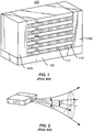
- FIG. 1 is a simplified perspective illustration of a two-dimensional array of diode lasers (i.e., semiconductor lasers).
- the diode laser array 100 includes a number of diode laser bars 110 stacked together with heat exchangers 120 on a base 130.
- the heat exchangers 120 may be actively cooled micro-channel heat exchangers or the like.
- Heat conductors 140a and 140b may be utilized to provide an additional thermal path for removal of heat generated by the laser diode bars 110.
- Each individual laser bar includes a horizontally disposed array of lasers 112, each emitting pump radiation.
- the diode laser array 100 includes M x N lasers, where M is the number of diode laser bars 110 and N is the number of lasers 112 per bar.
- diode laser pump arrays typically provide anisotropic (uneven) illumination.
- FIG. 2 because of the generally oval shape of the beam at the laser facet, the divergence of an output beam from a diode laser is anisotropic, with the divergence angle in the vertical plane ( ⁇ V ) being significantly greater than the divergence angle in the horizontal direction ( ⁇ H ).
- Lenslet arrays mounted in front of the diode laser bars, with a horizontally disposed lenslet array matched to each horizontal laser bar, have been used to decrease the divergence angle in the vertical plane to a value approximately equal to the divergence angle in the horizontal direction.
- the present invention relates generally to laser systems. More particularly, the present invention relates to a method and system for homogenizing the output from a diode laser array.
- the method and apparatus have been applied to a diffractive photo-thermo-reflective glass member optically coupled to a diode laser array to provide an output with a substantially uniform intensity profile.
- methods of fabricating large diffractive homogenizers are provided by embodiments of the present invention. It will be recognized that the invention has a much broader range of applicability and can be applied to other laser systems.
- an optical amplifier system includes a diode pump array including a plurality of semiconductor diode laser bars disposed in an array configuration and characterized by a periodic distance between adjacent semiconductor diode laser bars. The periodic distance is measured in a first direction perpendicular to each of the plurality of semiconductor diode laser bars.
- the diode pump array provides a pump output propagating along an optical path and characterized by a first intensity profile measured as a function of the first direction and having a variation greater than 10%.
- the optical amplifier system also includes a diffractive optic disposed along the optical path.
- the diffractive optic includes a photo-thermo-refractive glass member.
- the optical amplifier system further includes an amplifier slab having an input face and position along the optical path and separated from the diffractive optic by a predetermined distance. A second intensity profile measured at the input face of the amplifier slab as a function of the first direction has a variation less than 10%.
- a method of fabricating a diffractive homogenizer includes providing a partially transmissive optical element having a predetermined grayscale intensity pattern thereon, providing a transparent optical element, and directing UV radiation through the partially transmissive optical element to impinge on the transparent optical element.
- the method also includes exposing a predetermined portion of the transparent optical element to the UV radiation and thermally treating the transparent optical element to produce the diffractive homogenizer characterized by a continuously varying index of refraction profile as a function of position within the transparent optical element.
- the present technique provides for homogenization of diode illumination, resulting in a uniform intensity profile, higher extraction efficiency from solid state amplifiers and laser gain media, and improved beam quality for the output of the solid state amplifiers.
- transfer efficiency provided by embodiments of the present invention can exceed 98%.
- Embodiments of the present invention are applicable to high power solid state amplifiers as well as solid state lasers.
- embodiments of the present invention provide a method of manufacturing diffractive optics with smooth phase profiles, thereby improving homogenization and solid state amplifier/laser efficiency.
- Embodiments of the present invention homogenize the diode illumination, leading to even illumination and improved beam quality in high average power diode pumped solid state lasers. Even illumination enables improved laser extraction efficiency and a uniform thermal load which minimizes thermally induced wavefront distortions.
- the improved beam quality and wavefront further serve to enhance the reliability of the laser device since the fluence or intensity loading of optics in the system are lower relative to the laser induced optical damage threshold.
- FIG. 3 is a simplified plot of laser intensity as a function of position for two modules of diode laser arrays.
- two modules 300 are illustrated, each module including an array of laser bars 110 separated by heat spreaders 120.
- the modules can be similar to the diode laser pump array 100 illustrated in FIG. 1 .
- the intensity profile measured vertically down the module 300 will be non-uniform.
- the intensity profile has peaks associated with the laser bars 110, valleys associated with the heat spreaders 120 between the laser bars, and a larger valley between adjacent modules.
- the intensity profile illustrated in FIG. 3 is undesirable since such a pump intensity profile will result in non-uniformity in the gain profile of the amplifier. Non-uniformity in the gain profile of the amplifier (or laser) results in lower amplifier efficiency and degraded beam quality.
- diode laser pump light from each emitter or from a group of emitters can be launched into an optical fiber.
- an optical fiber to homogenize light from an emitter or group of emitters can improve the beam homogeneity, individual optical fibers are limited in power and employing this method is expensive and inefficient.
- Another approach has been transverse pumping of the amplifier slab so that the diode pumping of the slab is orthogonal to the direction of laser propagation.
- transverse pumping provides some benefits in improving the gain uniformity for small rods (e.g., rod diameter less than 1 cm) and small slab lasers and amplifiers
- scaling this method to larger apertures is difficult and prone to producing non-uniform gain across the aperture.
- Yet another approach is to use hollow reflective (or solid refractive) ducting to mix beams from multiple emitters. Although this technique provides some benefits, it is less efficient and more expensive than the techniques provided by embodiments of the present invention.
- photosensitive glass has been used to record a permanent image in silicate glass.
- a two-step process of exposure to UV radiation followed by thermal development resulted in a crystalline phase precipitation in the exposed areas, similar to a photographic process.
- a variety of different photosensitive glasses have been developed and been used in various applications, for example, photochromic eye glasses.
- PTR photo-thermo-refractive
- the elemental silver particles serve as nucleation centers for the growth of a second phase during the thermal development process, typically performed for several hours at a temperature of about 500 °C.
- This second phase is believed to be sodium and potassium halogenide rich, resulting in a lower index of refraction in exposed areas in comparison with unexposed areas.
- the refractive index change can also be controlled.
- planar slabs of PTR glass i.e., rectangular parallelepipeds
- diffractive homogenizers are used as diffractive homogenizers according to embodiments of the present invention.
- an interference pattern using two plane-wave -UV laser beams is created inside the PTR glass in order to induce a sinusoidal refractive index variation.
- Photorefractive glasses such as PTR glasses, have been used as a photosensitive medium to fabricate high-efficiency phase volume holograms used in communications systems, for example, wavelength division multiplexing (WDM) systems.
- WDM wavelength division multiplexing
- a linear refractive index modulation is achieved in the PTR glass after exposure to UV radiation followed by thermal treatment.
- PTR glass is a silicate glass, based on SiO2 and various additives.
- Exemplary grating-based diffractive elements include volume Bragg gratings (VBG) for angular beam combining, spectral beam combining, and mode locking.
- VBG volume Bragg gratings
- Exemplary VGB-based devices are available from OptiGrate Corp. of Orlando, Florida and PD-LD Inc. of Pennington, New Jersey.
- the conventional volume Bragg gratings are either periodic or chirped depending on the particular application and are fabricated by exposure using lasers as is typical with grating structures. Embodiments of the present invention contrast with these conventional grating structures formed in PTR since the pattern is not periodic or chirped, but defined based on the particular intensity profile present at the input face of the diffractive homogenizer and the desired intensity profile at the optical gain medium.
- the diffractive homogenizers provided by embodiments of the present invention are non-sinusoidal in contrast with grating based volume Bragg gratings.
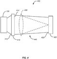
- FIG. 4 is a simplified schematic diagram of a diode laser array homogenization system according to an embodiment of the present invention.
- the diode laser array homogenization system includes a laser diode array 100 and a diffractive homogenizer 410.
- the diffractive homogenizer 410 is also referred to as a diffractive optical element.
- the diffractive homogenizer is fabricated using a slab of PTR glass (i.e., a rectangular parallelepiped of PTR glass).
- the surfaces 412 and 414 of the diffractive homogenizer are substantially planar and suitable for the deposition of antireflection (AR) coatings or other surface treatments.
- AR antireflection
- the diffractive homogenizer 410 is fabricated using a UV-based exposure and heat treatment process as described more fully throughout the present specification.
- PTR glass or other suitable transparent material that is able to provide a varying index of refraction as a function of position, enables the fabrication and use of a diffractive homogenizer with a continuous variation in refractive index as a function of position.
- diffractive homogenizers vary the phase on a spatial scale which is small relative to the diode illumination non-uniformity. This is in contrast to conventional etched diffractive optical elements in which discontinuities in the surface features result in an index of refraction that changes discontinuously.
- the refractive index change produced in the PTR is typically proportional to the incident light intensity during exposure.
- the diode laser array homogenization system 400 also includes a propagation path 440 between the diffractive homogenizer 410 and gain medium 420.
- the gain medium 420 can be an amplifier slab for high-power amplifier or an active component of laser.
- the design of the diffractive homogenizer 410 will be tailored to the intensity profile produced by the diode laser array 100. After propagating through the propagation path 440, the spatially dependent illumination produced by a diode laser array will be randomized, creating a homogenized beam for pumping of the amplifier slab or other suitable gain media.
- an optional lens 430 may also be employed to concentrate the homogenized diode pump beam.
- the shape of the beam can be varied using the diffractive homogenizer 410.
- a square or rectangular beam cross section from a two-dimensional diode laser array could be maintained at the gain medium 420 (e.g., an amplifier slab) or converted to a round beam at the gain medium 420.
- the diffractive homogenizer 410 can perform homogenization of the beam as well as imaging.
- a micro-lens array is utilized to collimate or partially collimate the light from the diode lasers.
- the diffractive homogenizer can include index of refraction variations effective to collimate the beam as well as remove the non-uniformities resulting from the geometry of the diode laser array.
- embodiments of the present invention do not require the use of a microlens array to collimate the light from the diode array.
- volume Bragg gratings for use in wavelength division multiplexing systems.
- These volume Bragg gratings are either periodic or chirped depending on the particular application and are fabricated by exposure using lasers as is typical with grating structures.
- Embodiments of the present invention contrast with these conventional grating structures formed in PTR since the pattern is not periodic or chirped, but defined based on the particular intensity profile present at the input face of the diffractive homogenizer and the desired intensity profile at the optical gain medium.
- the index of refraction profile in the diffractive homogenizer is thus defined in terms of the intensity profile at surface 412 and the desired uniform intensity profile at surface 422.
- embodiments of the present invention utilize a non-sinusoidal index of refraction profile to achieve the desired diffraction effects.
- Etched diffractive structures have a number of drawbacks that present problems for use in high power laser applications.
- the shape of the etched surface results in diffraction effects as a laser beam passes through the diffractive homogenizer.
- a high level of control is needed over the registration of one level of the etch mask to the other levels of the etch mask. Misalignment of the etch mask results in mis-defined surface shapes, thereby reducing the quality of the transmitted beam.
- the etch depth control is a critical input into the final surface profile. For an 8-level etch process with the total height of the diffraction feature being about 1 ⁇ m, the final step height is 250 nm, which is difficult to etch with a high level of repeatability.
- Embodiments of the present invention reduce or eliminate the shortcomings of etched diffractive optical elements.
- the planar surfaces associated with diffractive homogenizers made using PTR glass are well-suited to high-power laser applications. Because the surfaces of the optic are flat, collection of dirt and dust, common with etched surfaces, is reduced. Additionally, the flat surfaces provide a substrate suitable for deposition of AR coatings, reducing Fresnel reflection losses at interfaces.
- the flat surfaces and "internal" index variations provided by the diffractive homogenizers described herein result in much higher transfer efficiencies than those associated with etched diffraction structures. In contrast with a 16-level binary plate tested by the inventor, which was characterized by a transfer efficiency of about 80%, embodiments of the present invention provide transfer efficiencies of > 90%, > 92%, > 94%, > 96%, or > 98%.
- Embodiments of the present invention will be applicable to numerous high-power laser and amplifier applications.
- the LIFE program being developed at Lawrence Livermore National Laboratory, will utilize very large diode arrays and will benefit from the ability to deliver homogeneous light to the amplifiers. Homogenous illumination of the amplifiers will enable high beam quality and high efficiency.
- large aperture lasers useful for defense applications could also benefit from homogenous pumping to increase beam quality, which also increases the laser intensity on target for tactical warfare.
- Other diode pumped solid state laser applications such as laser machining, marking, drilling, and welding could also benefit from embodiments of the present invention by way of improved output energy and beam quality.
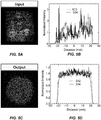
- FIG. 5A is a simplified image of laser intensity as a function of position at an input of the diffractive homogenizer according to an embodiment of the present invention.
- the intensity of the laser varies greatly as a function of position.
- the intensity profile is characterized by varying power as a function of position with some regions of the beam much brighter than other regions. In fact, several portions of the laser beam appear almost black, indicating low amounts of power at these portions of the beam.
- the light from the diode laser pump array has propagated a given distance and diffraction and propagation have resulted in the illustrated non-uniform intensity profile. If this intensity profile were imaged onto an amplifier slab, then the gain in the amplifier slab would be characterized by areas of high gain and areas of low gain, resulting in inefficient pumping of the gain medium in the amplifier. Moreover, the variation in the beam intensity will result in unpredictable gain profiles in the amplifier, adversely impacting system performance.
- FIG. 5B includes simplified plots of laser intensity as a function of position at the input of the diffractive homogenizer according to an embodiment of the present invention.
- An intensity profile taken along a horizontal direction is illustrated by dashed line 522 representing the width of the input beam and an intensity profile taken along a vertical direction is illustrated by solid line 524 representing the height of the input beam.
- the measurement along the width is characterized by an approximately bimodal distribution with peaks at the edge regions and a decrease in intensity at the middle of the profile.
- the measurement along the height (solid line 524) is characterized by the majority of power in the upper portion of the beam, with low intensity in the central in lower regions. A spike at the lower edge of the beam is visible in the laser intensity plot.
- the intensity variation across the laser beam is large, with some of the intensity spikes being more than three times larger than other intensity values.
- solid line 524 associated with a vertical measurement through the beam the spikes at about -20 mm have a normalized intensity value greater than three, whereas the intensity at about -10 mm is less than one.
- dashed line 522 which has an average normalized intensity value of around one, some peaks reach about twice that value, with troughs down to about half that value. Thus, variations in the intensity can be greater than 100%.
- a laser beam with the intensity profile as illustrated in FIG. 5B will result in poor performance when used as a pump beam or for other high-power applications. Focusing of the input beam illustrated in FIGS. 5A and 5B will result in a non-diffraction limited spot, with significant amounts of power in higher-order lobes. Thus, the power on target will be far less than available had the input beam been uniform.
- FIG. 5C is a simplified image of laser intensity as a function of position at an output of the diffractive homogenizer according to an embodiment of the present invention.
- the output beam may be positioned at a surface 422 of the gain medium 420.
- the laser beam has been converted from a generally rectangular beam shape into a circular beam. Conversion of the beam shape is not required by embodiments of the present invention, but can be provided as illustrated in this figure.
- the image of laser beam intensity shows a uniform intensity pattern as a function of position, which is desirable for many applications.
- FIG. 5D includes simplified plots of laser intensity as a function of position at the output of the diffractive homogenizer according to an embodiment of the present invention.
- the laser intensity as a function of position across the circular beam is illustrated by dashed line 532 and solid line 534.
- the intensity profile taken along the horizontal direction is illustrated by dashed line 532 and the intensity profile taken along the vertical direction is illustrated by solid line 534.
- the intensity profiles in both the horizontal and vertical directions are substantially uniform, with only minor variations as a function of position.
- Utilizing the diffractive homogenizer described herein provides an intensity variation of less than 20% across the beam, less than 15%, less than 10%, less than 5%, less than 4%, less than 3%, less than 2%, or less than 1%, depending on the particular design criteria for the diffractive homogenizer.
- diffractive homogenizers are manufactured by using a master plate having either an intensity or phase variation and imaging a predetermined intensity profile on a photorefractive glass substrate, thereby creating a new diffractive homogenizer with a single exposure.
- FIG. 6 is a simplified flowchart illustrating a method of fabricating a diffractive homogenizer according to an embodiment of the present invention.
- one or more diffractive homogenizers can be fabricated for use in homogenization of light from a diode laser pump array.
- the method includes providing a partially transmissive slide (610) and a piece of PTR glass (612).
- the partially transmissive slide may be a photographic image suitable for use in grayscale photolithographic techniques.
- shades of gray can be utilized to produce continuous index of refraction changes as a function of position in the PTR glass. Based on computations of the desired index of refraction as a function of position in the PTR glass, the density of the partially transmissive slide, and the intensity of the illumination of the PTR glass as a result, will vary according to the amount of light to be exposed on the various portions of the PTR glass.
- the method also includes directing UV radiation through the partially transmissive slide to impinge on the PTR glass (614).
- the intensity pattern is a predetermined pattern as appropriate to the desired index of refraction pattern in the PTR glass.
- Predetermined portions of the PTR glass are exposed to UV radiation (616) and the exposed PTR glass is thermally treated to produce the desired index of refraction profile as a function of position.
- Some embodiments of the present invention provide a continuous variation in index of refraction as a function of position.
- the smoothly varying phase profile provided by these diffractive homogenizers enables higher transfer efficiency in generating the desired uniform beam profile.
- Another method that can be used to create the desired intensity profile on the PTR glass is to use a spatial light modulator to block portions of the UV beam and to create a continuously varying intensity pattern on the PTR glass.
- Image relay techniques utilized as a part of photolithographic processes can be utilized to magnify or demagnify images produced by either use of a partially transmissive slide or use of a spatial light modulator.
- the methods described herein can be scaled using a stepper to properly register one exposure site to the next, thereby timing together a complete large area diffractive homogenizer.
- a large area master plate fabricated using a tiling process can then be used to create duplicate plates utilizing a single exposure.
- Diffractive homogenizers fabricated in PTR glass are also more robust than conventional etched diffraction structures.
- the flat surfaces of the diffractive homogenizers provided according to embodiments of the present invention are much more difficult to damage than etched structures with fine features.
- an additional piece of PTR glass can be provided (620).
- UV radiation can be directed through the partially transmissive slide to impinge on the additional piece of PTR glass. Portions of the additional piece of PTR glass will be exposed to the UV radiation and the exposed PTR glass will then be thermally treated to provide a second diffractive homogenizer.
- This optional path can be performed multiple times.
- multiple diffractive homogenizers can be fabricated using a single partially transmissive slide as a master slide.
- the partially transmissive slide can be fabricated using a step and repeat process based on smaller sections of partially transmissive media.
- the disclosed methods of fabricating diffractive homogenizers including spatial beam homogenizers for diode laser arrays and laser beams, enables low-cost mass production at a scale limited only by the size of the substrate (e.g., PTR glass substrate).
- FIG. 6 provides a particular method of fabricating a diffractive homogenizer according to an embodiment of the present invention. Other sequences of steps may also be performed according to alternative embodiments. For example, alternative embodiments of the present invention may perform the steps outlined above in a different order. Moreover, the individual steps illustrated in FIG. 6 may include multiple sub-steps that may be performed in various sequences as appropriate to the individual step. Furthermore, additional steps may be added or removed depending on the particular applications. One of ordinary skill in the art would recognize many variations, modifications, and alternatives.
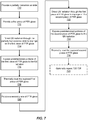
- FIG. 7 is a simplified flowchart illustrating a method of fabricating diffractive homogenizers according to another embodiment of the present invention.
- the method includes providing a partially transmissive slide (710) and a first piece of PTR glass (712). As described below, the first piece of PTR glass will be processed and then used as a master plate in producing additional pieces of PTR glass for use as diffractive homogenizers.
- the method also includes directing UV radiation through the partially transmissive slide to impinge on the first piece of PTR glass (714) and exposing predetermined portions of the first piece of PTR glass to the UV radiation (716).
- a two-dimensional spatial light modulator may be utilized to create a desired intensity pattern on the first piece of PTR glass thereby exposing predetermined portions of the first piece of PTR glass to UV radiation.
- the PTR glass After the PTR glass is exposed, it is thermally treated to produce a predetermined index of refraction pattern as a function of position inside PTR glass (718).
- the first piece of PTR glass is provided with index of refraction pattern that, through diffraction, will produce a predetermined intensity profile at a specified imaging plane.
- a computation is included in embodiments of the method in order to produce an intensity pattern on the first piece of PTR glass that will result in an index of refraction pattern that will subsequently be used to produce a second intensity pattern as described more fully below.
- Embodiments of the present invention can utilize several different methods to create the master plate.
- spatial light modulators In order to generate the desired light intensity profile for the master plate, spatial light modulators, lithographic printing techniques, standard photolithographic etching techniques, magneto-rheological finishing techniques, or the like can be used.
- the master plate After the master plate is fabricated, providing a phase plate with predetermined phase variation as a function of position across the plate, the master plate is used as a master for generating a nearly infinite number of duplicate plates, with the cost of the duplicate plate approaching that of the substrate used for the duplicate plate.
- the method further includes providing a second piece of PTR glass (720) and directing UV radiation through the first piece of PTR glass to impinge on the second piece of PTR glass (722).
- the first piece of PTR glass is thus used as a master plate in a manner analogous to the use of the partially transmissive slide. It will be appreciated that the partially transmissive slide is used to create a predetermined intensity pattern on the first piece of PTR glass.
- the first piece of PTR glass is now used to create a second predetermined intensity pattern on the second piece of PTR glass. Diffraction of the UV radiation passing through the first piece of PTR glass is utilized to form the second predetermined intensity pattern. Additional optical elements may be utilized as part of the optical system in order to form the second predetermined intensity pattern.
- One of ordinary skill in the art would recognize many variations, modifications, and alternatives.
- the second piece of PTR glass includes an index of refraction profile as a function of position that is suitable for use as a diffractive optical element, for example, a diffractive homogenizer.
- processes 720-726 are optionally repeated with additional pieces of PTR glass to form additional diffractive homogenizers.
- photolithographic techniques including image relay, magnification, demagnification, and the like, can be utilized during exposure of the PTR glass to UV radiation.
- FIG. 7 provides a particular method of fabricating diffractive homogenizers according to an embodiment of the present invention. Other sequences of steps may also be performed according to alternative embodiments. For example, alternative embodiments of the present invention may perform the steps outlined above in a different order. Moreover, the individual steps illustrated in FIG. 7 may include multiple sub-steps that may be performed in various sequences as appropriate to the individual step. Furthermore, additional steps may be added or removed depending on the particular applications. One of ordinary skill in the art would recognize many variations, modifications, and alternatives.
- FIG. 8 is a simplified flowchart illustrating a method of fabricating diffractive homogenizers using a master plate according to an embodiment of the present invention.
- the method includes providing a master plate characterized by a predetermined phase profile as a function of position (810).
- the master plate can be fabricated using PTR materials or may be a conventional multi-level etched diffractive element.
- the method also includes providing a piece of PTR glass (812) and directing UV radiation through the master slide to impinge on the PTR glass (814).
- the phase profile of the master plate is a predetermined phase profile that will cause light transmitted through the master plate to diffract and provide an intensity pattern at the piece of PTR glass.
- the method further includes exposing predetermined portions of the PTR glass to the UV radiation (816) and thermally treating the exposed PTR glass (818) to form a diffractive homogenizer.
- the methods illustrated in FIG. 8 share common features with those illustrated in FIGS. 6 and 7 and description associated with those figures is applicable to FIG. 8 .
- additional pieces of PTR glass are provided (820) and processes 814 through 818 are repeated to fabricate the additional diffractive homogenizers.
- a single phase-based master plate a plurality of identical diffractive homogenizers, with the cost of the diffractive homogenizers approaching that of the substrate used during fabrication.
- step and repeat methodologies may be utilized to fabricate diffractive homogenizers larger than the master plate.
- FIG. 8 provides a particular method of fabricating diffractive homogenizers using a master plate according to an embodiment of the present invention. Other sequences of steps may also be performed according to alternative embodiments. For example, alternative embodiments of the present invention may perform the steps outlined above in a different order. Moreover, the individual steps illustrated in FIG. 8 may include multiple sub-steps that may be performed in various sequences as appropriate to the individual step. Furthermore, additional steps may be added or removed depending on the particular applications. One of ordinary skill in the art would recognize many variations, modifications, and alternatives.
Landscapes
- Physics & Mathematics (AREA)
- Optics & Photonics (AREA)
- General Physics & Mathematics (AREA)
- Electromagnetism (AREA)
- Engineering & Computer Science (AREA)
- Plasma & Fusion (AREA)
- Manufacturing & Machinery (AREA)
- Diffracting Gratings Or Hologram Optical Elements (AREA)
- Lasers (AREA)
- Condensed Matter Physics & Semiconductors (AREA)
Applications Claiming Priority (3)
| Application Number | Priority Date | Filing Date | Title |
|---|---|---|---|
| US12/544,147 US8547632B2 (en) | 2009-08-19 | 2009-08-19 | Method and system for homogenizing diode laser pump arrays |
| US12/544,161 US8728719B2 (en) | 2009-08-19 | 2009-08-19 | Diffractive laser beam homogenizer including a photo-active material and method of fabricating the same |
| EP10008683.4A EP2287642B1 (de) | 2009-08-19 | 2010-08-19 | Diffraktiver Laserstrahlhomogenisator mit einem fotoaktiven Material und Herstellungsverfahren dafür |
Related Parent Applications (2)
| Application Number | Title | Priority Date | Filing Date |
|---|---|---|---|
| EP10008683.4A Division-Into EP2287642B1 (de) | 2009-08-19 | 2010-08-19 | Diffraktiver Laserstrahlhomogenisator mit einem fotoaktiven Material und Herstellungsverfahren dafür |
| EP10008683.4A Division EP2287642B1 (de) | 2009-08-19 | 2010-08-19 | Diffraktiver Laserstrahlhomogenisator mit einem fotoaktiven Material und Herstellungsverfahren dafür |
Publications (3)
| Publication Number | Publication Date |
|---|---|
| EP3709061A2 true EP3709061A2 (de) | 2020-09-16 |
| EP3709061A3 EP3709061A3 (de) | 2020-10-14 |
| EP3709061B1 EP3709061B1 (de) | 2022-12-14 |
Family
ID=43037851
Family Applications (3)
| Application Number | Title | Priority Date | Filing Date |
|---|---|---|---|
| EP10008684.2A Active EP2287643B1 (de) | 2009-08-19 | 2010-08-19 | Diffraktiver Laserstrahlhomogenisator mit einem fotoaktiven Material und Herstellungsverfahren dafür |
| EP10008683.4A Active EP2287642B1 (de) | 2009-08-19 | 2010-08-19 | Diffraktiver Laserstrahlhomogenisator mit einem fotoaktiven Material und Herstellungsverfahren dafür |
| EP20160366.9A Active EP3709061B1 (de) | 2009-08-19 | 2010-08-19 | Verfahren zur herstellung und verfahren zur verwendung einer diffraktiven optik |
Family Applications Before (2)
| Application Number | Title | Priority Date | Filing Date |
|---|---|---|---|
| EP10008684.2A Active EP2287643B1 (de) | 2009-08-19 | 2010-08-19 | Diffraktiver Laserstrahlhomogenisator mit einem fotoaktiven Material und Herstellungsverfahren dafür |
| EP10008683.4A Active EP2287642B1 (de) | 2009-08-19 | 2010-08-19 | Diffraktiver Laserstrahlhomogenisator mit einem fotoaktiven Material und Herstellungsverfahren dafür |
Country Status (2)
| Country | Link |
|---|---|
| US (1) | US9331452B2 (de) |
| EP (3) | EP2287643B1 (de) |
Families Citing this family (9)
| Publication number | Priority date | Publication date | Assignee | Title |
|---|---|---|---|---|
| EP3368314A4 (de) | 2015-10-30 | 2019-05-01 | Seurat Technologies, Inc. | Multifunktionales ingestersystem für generative fertigung |
| US12459200B2 (en) | 2017-05-11 | 2025-11-04 | Seurat Technologies, Inc. | Solid state routing of patterned light for additive manufacturing optimization |
| WO2017132664A1 (en) | 2016-01-28 | 2017-08-03 | Seurat Technologies, Inc. | Additive manufacturing, spatial heat treating system and method |
| WO2017132668A1 (en) | 2016-01-29 | 2017-08-03 | Seurat Technologies, Inc. | Additive manufacturing, bond modifying system and method |
| CN110869210B (zh) | 2017-05-11 | 2022-09-13 | 速尔特技术有限公司 | 用于增材制造的图案化光的开关站射束路由 |
| WO2020123828A1 (en) | 2018-12-14 | 2020-06-18 | Seurat Technologies, Inc | Additive manufacturing system for object creation from powder using a high flux laser for two-dimensional printing |
| KR102719019B1 (ko) | 2018-12-19 | 2024-10-18 | 쇠라 테크널러지스 인코포레이티드 | 2차원 인쇄를 위해 펄스 변조 레이저를 사용하는 적층 제조 시스템 |
| CN110879433B (zh) * | 2019-11-25 | 2021-01-01 | 中国科学院上海光学精密机械研究所 | 一种基于光热折变玻璃的反射式体光栅制备方法 |
| US12162074B2 (en) | 2020-11-25 | 2024-12-10 | Lawrence Livermore National Security, Llc | System and method for large-area pulsed laser melting of metallic powder in a laser powder bed fusion application |
Family Cites Families (49)
| Publication number | Priority date | Publication date | Assignee | Title |
|---|---|---|---|---|
| DE2951207A1 (de) | 1978-12-26 | 1980-07-10 | Canon Kk | Verfahren zur optischen herstellung einer streuplatte |
| US4427265A (en) | 1980-06-27 | 1984-01-24 | Canon Kabushiki Kaisha | Diffusion plate |
| US4547037A (en) | 1980-10-16 | 1985-10-15 | Regents Of The University Of Minnesota | Holographic method for producing desired wavefront transformations |
| JPS57148728A (en) | 1981-03-11 | 1982-09-14 | Canon Inc | Diffusing plate |
| US4572611A (en) | 1983-08-04 | 1986-02-25 | Corning Glass Works | Apparatus including an integral optical device |
| US4514053A (en) | 1983-08-04 | 1985-04-30 | Corning Glass Works | Integral photosensitive optical device and method |
| US4968117A (en) * | 1983-09-02 | 1990-11-06 | Hughes Aircraft Company | Graded index asperhic combiners and display system utilizing same |
| US5333077A (en) * | 1989-10-31 | 1994-07-26 | Massachusetts Inst Technology | Method and apparatus for efficient concentration of light from laser diode arrays |
| US5307365A (en) | 1991-08-08 | 1994-04-26 | Northrop Corporation | Cavity pumped, solid state lasers |
| JPH06118863A (ja) | 1992-09-30 | 1994-04-28 | Toppan Printing Co Ltd | カラーリップマンホログラムの作製方法 |
| US5327515A (en) | 1993-01-14 | 1994-07-05 | At&T Laboratories | Method for forming a Bragg grating in an optical medium |
| WO1995003935A1 (en) | 1993-07-27 | 1995-02-09 | Physical Optics Corporation | Light source destructuring and shaping device |
| US5610733A (en) | 1994-02-28 | 1997-03-11 | Digital Optics Corporation | Beam-homogenizer |
| US5615022A (en) | 1994-08-22 | 1997-03-25 | Grumman Aerospace Corporation | System and method of fabricating multiple holographic elements |
| DE4443029A1 (de) | 1994-12-02 | 1996-06-27 | Bundesdruckerei Gmbh | Masterhologramm zur Herstellung von kopiersicheren Hologrammen |
| DE19632460C1 (de) | 1996-08-12 | 1997-10-30 | Microlas Lasersystem Gmbh | Optische Vorrichtung zum Homogenisieren von Laserstrahlung und Erzeugen von mehreren Beleuchtungsfeldern |
| US6562523B1 (en) | 1996-10-31 | 2003-05-13 | Canyon Materials, Inc. | Direct write all-glass photomask blanks |
| US5999281A (en) | 1997-02-28 | 1999-12-07 | Polaroid Corporation | Holographic projection screen combining an elliptical holographic diffuser and a cylindrical light-collimator |
| JP4302885B2 (ja) | 1998-01-29 | 2009-07-29 | ビジックス, インコーポレイテッド | 回折性の光学的ビーム積分によるレーザー伝送システムおよび方法 |
| US6271957B1 (en) | 1998-05-29 | 2001-08-07 | Affymetrix, Inc. | Methods involving direct write optical lithography |
| US6215598B1 (en) | 1998-10-05 | 2001-04-10 | Ruey Jennifer Hwu | Apparatus and method for concentrating beams from broad area diode lasers, diode laser bars and/ or diode laser arrays |
| US6594299B1 (en) | 1998-11-12 | 2003-07-15 | Mitsubishi Denki Kabushiki Kaisha | Semiconductor laser light emitting apparatus and solid-state laser rod pumping module |
| JP2001174615A (ja) * | 1999-04-15 | 2001-06-29 | Nikon Corp | 回折光学素子、該素子の製造方法、該素子を備える照明装置、投影露光装置、露光方法、及び光ホモジナイザー、該光ホモジナイザーの製造方法 |
| KR100334812B1 (ko) | 1999-07-02 | 2002-05-02 | 윤종용 | 아포다이즈드 광섬유 격자 제작장치 |
| FR2796728B1 (fr) | 1999-07-21 | 2003-06-27 | France Telecom | Procede d'apodisation de reseau de bragg photoinscrit |
| KR100315672B1 (ko) * | 1999-12-28 | 2001-11-29 | 윤종용 | 진폭 마스크를 이용한 절족화된 광섬유 격자의 제작 방법 |
| US6586141B1 (en) * | 2000-01-04 | 2003-07-01 | University Of Central Florida | Process for production of high efficiency volume diffractive elements in photo-thermo-refractive glass |
| US6673497B2 (en) * | 2000-01-04 | 2004-01-06 | University Of Central Florida | High efficiency volume diffractive elements in photo-thermo-refractive glass |
| US20030107787A1 (en) | 2001-09-26 | 2003-06-12 | Arkady Bablumyan | Planar and fiber optical apodized diffraction structures fabrication |
| US6700709B1 (en) | 2002-03-01 | 2004-03-02 | Boston Laser Inc. | Configuration of and method for optical beam shaping of diode laser bars |
| WO2003079058A2 (en) | 2002-03-15 | 2003-09-25 | Pd-Ld, Inc. | Fiber optic devices having volume bragg grating elements |
| JP2004126312A (ja) | 2002-10-03 | 2004-04-22 | Japan Science & Technology Corp | 三次元ホログラフィック記録方法および三次元ホログラフィック記録装置 |
| JP2006502439A (ja) | 2002-10-04 | 2006-01-19 | コーニング インコーポレイテッド | レンズアレイ、そのレンズアレイの製造方法および感光性ガラスプレート |
| JP2007508596A (ja) | 2003-10-17 | 2007-04-05 | エクスプレイ リミテッド | 投影システムに使用する光学システムおよび方法 |
| JP4473617B2 (ja) | 2004-03-26 | 2010-06-02 | 浜松ホトニクス株式会社 | 固体レーザ媒質の励起分布を制御する装置および方法 |
| JP2005326666A (ja) * | 2004-05-14 | 2005-11-24 | Sumitomo Electric Ind Ltd | 屈折率変調型回折光学素子とそれを含むプロジェクタ |
| DE102004040608B4 (de) | 2004-08-21 | 2006-09-07 | Dilas Diodenlaser Gmbh | Diodenlaser mit einer optischen Einrichtung zur Erhöhung der Strahldichte eines aus ihm austretenden Ausgangslaserstrahls |
| US20060045144A1 (en) | 2004-09-01 | 2006-03-02 | Nlight Photonics Corporation | Diode laser array beam homogenizer |
| US7590160B2 (en) * | 2004-11-26 | 2009-09-15 | Manni Jeffrey G | High-gain diode-pumped laser amplifier |
| DE102005003594B4 (de) * | 2004-12-31 | 2016-02-18 | Schott Ag | Verfahren zur Herstellung eines optischen Bauteils, verfahrensgemäß hergestelltes Bauteil sowie derartige Bauteile umfassende Einrichtung |
| JP2007121941A (ja) * | 2005-10-31 | 2007-05-17 | Kyocera Corp | ファイバ状位相格子素子、ファイバ状位相格子および位相格子モジュール |
| WO2007069660A1 (ja) * | 2005-12-15 | 2007-06-21 | Asahi Glass Co., Ltd. | 波長選択回折素子及び光ヘッド装置 |
| KR101270538B1 (ko) | 2006-07-12 | 2013-06-03 | 삼성전자주식회사 | 식기세척기 |
| JP2008170471A (ja) * | 2007-01-05 | 2008-07-24 | Kyocera Corp | ファイバレンズ、ファイバレンズアレイ、ファイバコリメータおよび光モジュール |
| US20080254372A1 (en) * | 2007-04-13 | 2008-10-16 | Canyon Materials, Inc. | PDR and PBR glasses for holographic data storage and/or computer generated holograms |
| US7551818B2 (en) | 2007-09-28 | 2009-06-23 | The Aerospace Corporation | High power optical fiber laser array holographic coupler manufacturing method |
| US20090190214A1 (en) | 2008-01-29 | 2009-07-30 | Nicholas Francis Borrelli | Polarizing photorefractive glass |
| US8547632B2 (en) | 2009-08-19 | 2013-10-01 | Lawrence Livermore National Security, Llc | Method and system for homogenizing diode laser pump arrays |
| US8728719B2 (en) * | 2009-08-19 | 2014-05-20 | Lawrence Livermore National Security, Llc | Diffractive laser beam homogenizer including a photo-active material and method of fabricating the same |
-
2010
- 2010-08-19 EP EP10008684.2A patent/EP2287643B1/de active Active
- 2010-08-19 EP EP10008683.4A patent/EP2287642B1/de active Active
- 2010-08-19 EP EP20160366.9A patent/EP3709061B1/de active Active
-
2013
- 2013-06-06 US US13/911,787 patent/US9331452B2/en active Active
Also Published As
| Publication number | Publication date |
|---|---|
| EP2287642A2 (de) | 2011-02-23 |
| EP2287642B1 (de) | 2020-04-08 |
| US20140362432A1 (en) | 2014-12-11 |
| US9331452B2 (en) | 2016-05-03 |
| EP3709061B1 (de) | 2022-12-14 |
| EP3709061A3 (de) | 2020-10-14 |
| EP2287642A3 (de) | 2011-05-18 |
| EP2287643A1 (de) | 2011-02-23 |
| EP2287643B1 (de) | 2020-05-06 |
Similar Documents
| Publication | Publication Date | Title |
|---|---|---|
| US8547632B2 (en) | Method and system for homogenizing diode laser pump arrays | |
| US9331452B2 (en) | Method and system for homogenizing diode laser pump arrays | |
| US8728719B2 (en) | Diffractive laser beam homogenizer including a photo-active material and method of fabricating the same | |
| US6835535B2 (en) | Microlens arrays having high focusing efficiency | |
| US8730455B2 (en) | Illumination system for a microlithographic projection exposure apparatus | |
| CN102799079B (zh) | 用于微光刻投影曝光设备的照射系统 | |
| JP7309686B2 (ja) | 拡散板 | |
| EP3916436A1 (de) | Diffusionsplatte | |
| Yang et al. | Analysis and optimization on single-zone binary flat-top beam shaper | |
| KR20050044502A (ko) | 호모제니저 | |
| US7092165B2 (en) | Microlens arrays having high focusing efficiency | |
| CN114047569B (zh) | 一种实现一字线光斑的渐变周期光栅衍射元件及方法 | |
| WO2022172918A1 (ja) | 拡散板 | |
| CN108646429B (zh) | 一种结构光投影仪 | |
| Baehr et al. | Realization of refractive continuous-phase elements with high design freedom by mask-structured ion exchange | |
| Wippermann et al. | Improved homogenization of fly's eye condenser setups under coherent illumination using chirped microlens arrays | |
| WO2002010805A1 (en) | Microlens arrays having high focusing efficiency | |
| JP6183635B2 (ja) | オプティカルインテグレータ、照明ユニット、伝送光学系、照明光学系、露光装置、およびデバイス製造方法 | |
| Wippermann et al. | Comparison of fly's eye condensers based on regular, chirped, and stochastic tandem microlens arrays |
Legal Events
| Date | Code | Title | Description |
|---|---|---|---|
| PUAI | Public reference made under article 153(3) epc to a published international application that has entered the european phase |
Free format text: ORIGINAL CODE: 0009012 |
|
| STAA | Information on the status of an ep patent application or granted ep patent |
Free format text: STATUS: THE APPLICATION HAS BEEN PUBLISHED |
|
| PUAL | Search report despatched |
Free format text: ORIGINAL CODE: 0009013 |
|
| AC | Divisional application: reference to earlier application |
Ref document number: 2287642 Country of ref document: EP Kind code of ref document: P |
|
| AK | Designated contracting states |
Kind code of ref document: A2 Designated state(s): AL AT BE BG CH CY CZ DE DK EE ES FI FR GB GR HR HU IE IS IT LI LT LU LV MC MK MT NL NO PL PT RO SE SI SK SM TR |
|
| AK | Designated contracting states |
Kind code of ref document: A3 Designated state(s): AL AT BE BG CH CY CZ DE DK EE ES FI FR GB GR HR HU IE IS IT LI LT LU LV MC MK MT NL NO PL PT RO SE SI SK SM TR |
|
| RIC1 | Information provided on ipc code assigned before grant |
Ipc: H01S 5/40 20060101ALI20200908BHEP Ipc: G02B 5/18 20060101AFI20200908BHEP Ipc: G02B 6/02 20060101ALI20200908BHEP Ipc: G02B 27/09 20060101ALI20200908BHEP Ipc: H01S 3/0941 20060101ALI20200908BHEP |
|
| STAA | Information on the status of an ep patent application or granted ep patent |
Free format text: STATUS: REQUEST FOR EXAMINATION WAS MADE |
|
| 17P | Request for examination filed |
Effective date: 20210414 |
|
| RBV | Designated contracting states (corrected) |
Designated state(s): AL AT BE BG CH CY CZ DE DK EE ES FI FR GB GR HR HU IE IS IT LI LT LU LV MC MK MT NL NO PL PT RO SE SI SK SM TR |
|
| GRAP | Despatch of communication of intention to grant a patent |
Free format text: ORIGINAL CODE: EPIDOSNIGR1 |
|
| STAA | Information on the status of an ep patent application or granted ep patent |
Free format text: STATUS: GRANT OF PATENT IS INTENDED |
|
| INTG | Intention to grant announced |
Effective date: 20220629 |
|
| GRAS | Grant fee paid |
Free format text: ORIGINAL CODE: EPIDOSNIGR3 |
|
| GRAA | (expected) grant |
Free format text: ORIGINAL CODE: 0009210 |
|
| STAA | Information on the status of an ep patent application or granted ep patent |
Free format text: STATUS: THE PATENT HAS BEEN GRANTED |
|
| AC | Divisional application: reference to earlier application |
Ref document number: 2287642 Country of ref document: EP Kind code of ref document: P |
|
| AK | Designated contracting states |
Kind code of ref document: B1 Designated state(s): AL AT BE BG CH CY CZ DE DK EE ES FI FR GB GR HR HU IE IS IT LI LT LU LV MC MK MT NL NO PL PT RO SE SI SK SM TR |
|
| REG | Reference to a national code |
Ref country code: GB Ref legal event code: FG4D |
|
| REG | Reference to a national code |
Ref country code: CH Ref legal event code: EP |
|
| REG | Reference to a national code |
Ref country code: DE Ref legal event code: R096 Ref document number: 602010068629 Country of ref document: DE |
|
| REG | Reference to a national code |
Ref country code: IE Ref legal event code: FG4D |
|
| REG | Reference to a national code |
Ref country code: AT Ref legal event code: REF Ref document number: 1538021 Country of ref document: AT Kind code of ref document: T Effective date: 20230115 |
|
| REG | Reference to a national code |
Ref country code: LT Ref legal event code: MG9D |
|
| REG | Reference to a national code |
Ref country code: NL Ref legal event code: MP Effective date: 20221214 |
|
| PG25 | Lapsed in a contracting state [announced via postgrant information from national office to epo] |
Ref country code: SE Free format text: LAPSE BECAUSE OF FAILURE TO SUBMIT A TRANSLATION OF THE DESCRIPTION OR TO PAY THE FEE WITHIN THE PRESCRIBED TIME-LIMIT Effective date: 20221214 Ref country code: NO Free format text: LAPSE BECAUSE OF FAILURE TO SUBMIT A TRANSLATION OF THE DESCRIPTION OR TO PAY THE FEE WITHIN THE PRESCRIBED TIME-LIMIT Effective date: 20230314 Ref country code: LT Free format text: LAPSE BECAUSE OF FAILURE TO SUBMIT A TRANSLATION OF THE DESCRIPTION OR TO PAY THE FEE WITHIN THE PRESCRIBED TIME-LIMIT Effective date: 20221214 Ref country code: FI Free format text: LAPSE BECAUSE OF FAILURE TO SUBMIT A TRANSLATION OF THE DESCRIPTION OR TO PAY THE FEE WITHIN THE PRESCRIBED TIME-LIMIT Effective date: 20221214 |
|
| REG | Reference to a national code |
Ref country code: AT Ref legal event code: MK05 Ref document number: 1538021 Country of ref document: AT Kind code of ref document: T Effective date: 20221214 |
|
| PG25 | Lapsed in a contracting state [announced via postgrant information from national office to epo] |
Ref country code: LV Free format text: LAPSE BECAUSE OF FAILURE TO SUBMIT A TRANSLATION OF THE DESCRIPTION OR TO PAY THE FEE WITHIN THE PRESCRIBED TIME-LIMIT Effective date: 20221214 Ref country code: HR Free format text: LAPSE BECAUSE OF FAILURE TO SUBMIT A TRANSLATION OF THE DESCRIPTION OR TO PAY THE FEE WITHIN THE PRESCRIBED TIME-LIMIT Effective date: 20221214 Ref country code: GR Free format text: LAPSE BECAUSE OF FAILURE TO SUBMIT A TRANSLATION OF THE DESCRIPTION OR TO PAY THE FEE WITHIN THE PRESCRIBED TIME-LIMIT Effective date: 20230315 |
|
| P01 | Opt-out of the competence of the unified patent court (upc) registered |
Effective date: 20230425 |
|
| P02 | Opt-out of the competence of the unified patent court (upc) changed |
Effective date: 20230512 |
|
| PG25 | Lapsed in a contracting state [announced via postgrant information from national office to epo] |
Ref country code: NL Free format text: LAPSE BECAUSE OF FAILURE TO SUBMIT A TRANSLATION OF THE DESCRIPTION OR TO PAY THE FEE WITHIN THE PRESCRIBED TIME-LIMIT Effective date: 20221214 |
|
| PG25 | Lapsed in a contracting state [announced via postgrant information from national office to epo] |
Ref country code: SM Free format text: LAPSE BECAUSE OF FAILURE TO SUBMIT A TRANSLATION OF THE DESCRIPTION OR TO PAY THE FEE WITHIN THE PRESCRIBED TIME-LIMIT Effective date: 20221214 Ref country code: RO Free format text: LAPSE BECAUSE OF FAILURE TO SUBMIT A TRANSLATION OF THE DESCRIPTION OR TO PAY THE FEE WITHIN THE PRESCRIBED TIME-LIMIT Effective date: 20221214 Ref country code: PT Free format text: LAPSE BECAUSE OF FAILURE TO SUBMIT A TRANSLATION OF THE DESCRIPTION OR TO PAY THE FEE WITHIN THE PRESCRIBED TIME-LIMIT Effective date: 20230414 Ref country code: ES Free format text: LAPSE BECAUSE OF FAILURE TO SUBMIT A TRANSLATION OF THE DESCRIPTION OR TO PAY THE FEE WITHIN THE PRESCRIBED TIME-LIMIT Effective date: 20221214 Ref country code: EE Free format text: LAPSE BECAUSE OF FAILURE TO SUBMIT A TRANSLATION OF THE DESCRIPTION OR TO PAY THE FEE WITHIN THE PRESCRIBED TIME-LIMIT Effective date: 20221214 Ref country code: CZ Free format text: LAPSE BECAUSE OF FAILURE TO SUBMIT A TRANSLATION OF THE DESCRIPTION OR TO PAY THE FEE WITHIN THE PRESCRIBED TIME-LIMIT Effective date: 20221214 Ref country code: AT Free format text: LAPSE BECAUSE OF FAILURE TO SUBMIT A TRANSLATION OF THE DESCRIPTION OR TO PAY THE FEE WITHIN THE PRESCRIBED TIME-LIMIT Effective date: 20221214 |
|
| PG25 | Lapsed in a contracting state [announced via postgrant information from national office to epo] |
Ref country code: SK Free format text: LAPSE BECAUSE OF FAILURE TO SUBMIT A TRANSLATION OF THE DESCRIPTION OR TO PAY THE FEE WITHIN THE PRESCRIBED TIME-LIMIT Effective date: 20221214 Ref country code: PL Free format text: LAPSE BECAUSE OF FAILURE TO SUBMIT A TRANSLATION OF THE DESCRIPTION OR TO PAY THE FEE WITHIN THE PRESCRIBED TIME-LIMIT Effective date: 20221214 Ref country code: IS Free format text: LAPSE BECAUSE OF FAILURE TO SUBMIT A TRANSLATION OF THE DESCRIPTION OR TO PAY THE FEE WITHIN THE PRESCRIBED TIME-LIMIT Effective date: 20230414 Ref country code: AL Free format text: LAPSE BECAUSE OF FAILURE TO SUBMIT A TRANSLATION OF THE DESCRIPTION OR TO PAY THE FEE WITHIN THE PRESCRIBED TIME-LIMIT Effective date: 20221214 |
|
| REG | Reference to a national code |
Ref country code: DE Ref legal event code: R097 Ref document number: 602010068629 Country of ref document: DE |
|
| PLBE | No opposition filed within time limit |
Free format text: ORIGINAL CODE: 0009261 |
|
| STAA | Information on the status of an ep patent application or granted ep patent |
Free format text: STATUS: NO OPPOSITION FILED WITHIN TIME LIMIT |
|
| PG25 | Lapsed in a contracting state [announced via postgrant information from national office to epo] |
Ref country code: DK Free format text: LAPSE BECAUSE OF FAILURE TO SUBMIT A TRANSLATION OF THE DESCRIPTION OR TO PAY THE FEE WITHIN THE PRESCRIBED TIME-LIMIT Effective date: 20221214 |
|
| 26N | No opposition filed |
Effective date: 20230915 |
|
| PG25 | Lapsed in a contracting state [announced via postgrant information from national office to epo] |
Ref country code: SI Free format text: LAPSE BECAUSE OF FAILURE TO SUBMIT A TRANSLATION OF THE DESCRIPTION OR TO PAY THE FEE WITHIN THE PRESCRIBED TIME-LIMIT Effective date: 20221214 |
|
| PG25 | Lapsed in a contracting state [announced via postgrant information from national office to epo] |
Ref country code: MC Free format text: LAPSE BECAUSE OF FAILURE TO SUBMIT A TRANSLATION OF THE DESCRIPTION OR TO PAY THE FEE WITHIN THE PRESCRIBED TIME-LIMIT Effective date: 20221214 |
|
| REG | Reference to a national code |
Ref country code: CH Ref legal event code: PL |
|
| PG25 | Lapsed in a contracting state [announced via postgrant information from national office to epo] |
Ref country code: MC Free format text: LAPSE BECAUSE OF FAILURE TO SUBMIT A TRANSLATION OF THE DESCRIPTION OR TO PAY THE FEE WITHIN THE PRESCRIBED TIME-LIMIT Effective date: 20221214 |
|
| PG25 | Lapsed in a contracting state [announced via postgrant information from national office to epo] |
Ref country code: LU Free format text: LAPSE BECAUSE OF NON-PAYMENT OF DUE FEES Effective date: 20230819 |
|
| PG25 | Lapsed in a contracting state [announced via postgrant information from national office to epo] |
Ref country code: LU Free format text: LAPSE BECAUSE OF NON-PAYMENT OF DUE FEES Effective date: 20230819 Ref country code: CH Free format text: LAPSE BECAUSE OF NON-PAYMENT OF DUE FEES Effective date: 20230831 |
|
| REG | Reference to a national code |
Ref country code: BE Ref legal event code: MM Effective date: 20230831 |
|
| REG | Reference to a national code |
Ref country code: IE Ref legal event code: MM4A |
|
| PG25 | Lapsed in a contracting state [announced via postgrant information from national office to epo] |
Ref country code: IT Free format text: LAPSE BECAUSE OF FAILURE TO SUBMIT A TRANSLATION OF THE DESCRIPTION OR TO PAY THE FEE WITHIN THE PRESCRIBED TIME-LIMIT Effective date: 20221214 |
|
| PG25 | Lapsed in a contracting state [announced via postgrant information from national office to epo] |
Ref country code: IE Free format text: LAPSE BECAUSE OF NON-PAYMENT OF DUE FEES Effective date: 20230819 |
|
| PG25 | Lapsed in a contracting state [announced via postgrant information from national office to epo] |
Ref country code: IE Free format text: LAPSE BECAUSE OF NON-PAYMENT OF DUE FEES Effective date: 20230819 |
|
| PG25 | Lapsed in a contracting state [announced via postgrant information from national office to epo] |
Ref country code: BE Free format text: LAPSE BECAUSE OF NON-PAYMENT OF DUE FEES Effective date: 20230831 |
|
| PG25 | Lapsed in a contracting state [announced via postgrant information from national office to epo] |
Ref country code: BG Free format text: LAPSE BECAUSE OF FAILURE TO SUBMIT A TRANSLATION OF THE DESCRIPTION OR TO PAY THE FEE WITHIN THE PRESCRIBED TIME-LIMIT Effective date: 20221214 |
|
| PG25 | Lapsed in a contracting state [announced via postgrant information from national office to epo] |
Ref country code: BG Free format text: LAPSE BECAUSE OF FAILURE TO SUBMIT A TRANSLATION OF THE DESCRIPTION OR TO PAY THE FEE WITHIN THE PRESCRIBED TIME-LIMIT Effective date: 20221214 |
|
| PG25 | Lapsed in a contracting state [announced via postgrant information from national office to epo] |
Ref country code: CY Free format text: LAPSE BECAUSE OF FAILURE TO SUBMIT A TRANSLATION OF THE DESCRIPTION OR TO PAY THE FEE WITHIN THE PRESCRIBED TIME-LIMIT; INVALID AB INITIO Effective date: 20100819 |
|
| PG25 | Lapsed in a contracting state [announced via postgrant information from national office to epo] |
Ref country code: HU Free format text: LAPSE BECAUSE OF FAILURE TO SUBMIT A TRANSLATION OF THE DESCRIPTION OR TO PAY THE FEE WITHIN THE PRESCRIBED TIME-LIMIT; INVALID AB INITIO Effective date: 20100819 |
|
| PGFP | Annual fee paid to national office [announced via postgrant information from national office to epo] |
Ref country code: DE Payment date: 20250827 Year of fee payment: 16 |
|
| PGFP | Annual fee paid to national office [announced via postgrant information from national office to epo] |
Ref country code: GB Payment date: 20250827 Year of fee payment: 16 |
|
| PGFP | Annual fee paid to national office [announced via postgrant information from national office to epo] |
Ref country code: FR Payment date: 20250825 Year of fee payment: 16 |
|
| PG25 | Lapsed in a contracting state [announced via postgrant information from national office to epo] |
Ref country code: TR Free format text: LAPSE BECAUSE OF FAILURE TO SUBMIT A TRANSLATION OF THE DESCRIPTION OR TO PAY THE FEE WITHIN THE PRESCRIBED TIME-LIMIT Effective date: 20221214 |