EP3708384A1 - Verkleidungselement oder zifferblatt einer uhr oder eines schmuckstücks aus leitendem material - Google Patents
Verkleidungselement oder zifferblatt einer uhr oder eines schmuckstücks aus leitendem material Download PDFInfo
- Publication number
- EP3708384A1 EP3708384A1 EP19162928.6A EP19162928A EP3708384A1 EP 3708384 A1 EP3708384 A1 EP 3708384A1 EP 19162928 A EP19162928 A EP 19162928A EP 3708384 A1 EP3708384 A1 EP 3708384A1
- Authority
- EP
- European Patent Office
- Prior art keywords
- layer
- covering
- carried out
- during
- metallic
- Prior art date
- Legal status (The legal status is an assumption and is not a legal conclusion. Google has not performed a legal analysis and makes no representation as to the accuracy of the status listed.)
- Pending
Links
- 239000004020 conductor Substances 0.000 title claims abstract description 10
- 238000005034 decoration Methods 0.000 claims abstract description 55
- 238000011282 treatment Methods 0.000 claims abstract description 53
- 239000000463 material Substances 0.000 claims abstract description 38
- 238000004519 manufacturing process Methods 0.000 claims abstract description 16
- 230000001681 protective effect Effects 0.000 claims abstract description 11
- 239000010410 layer Substances 0.000 claims description 108
- 238000000034 method Methods 0.000 claims description 55
- 238000005530 etching Methods 0.000 claims description 51
- 239000011241 protective layer Substances 0.000 claims description 23
- 239000000126 substance Substances 0.000 claims description 21
- 239000000758 substrate Substances 0.000 claims description 18
- 238000000151 deposition Methods 0.000 claims description 15
- VYZAMTAEIAYCRO-UHFFFAOYSA-N Chromium Chemical compound [Cr] VYZAMTAEIAYCRO-UHFFFAOYSA-N 0.000 claims description 13
- 239000000919 ceramic Substances 0.000 claims description 13
- 230000008021 deposition Effects 0.000 claims description 12
- 229910052782 aluminium Inorganic materials 0.000 claims description 11
- XAGFODPZIPBFFR-UHFFFAOYSA-N aluminium Chemical compound [Al] XAGFODPZIPBFFR-UHFFFAOYSA-N 0.000 claims description 11
- 229910052804 chromium Inorganic materials 0.000 claims description 10
- 239000011651 chromium Substances 0.000 claims description 10
- 150000001875 compounds Chemical class 0.000 claims description 9
- 229910052737 gold Inorganic materials 0.000 claims description 9
- 239000010931 gold Substances 0.000 claims description 9
- 229910052751 metal Inorganic materials 0.000 claims description 9
- 239000002184 metal Substances 0.000 claims description 9
- 238000004140 cleaning Methods 0.000 claims description 6
- PCHJSUWPFVWCPO-UHFFFAOYSA-N gold Chemical compound [Au] PCHJSUWPFVWCPO-UHFFFAOYSA-N 0.000 claims description 6
- BASFCYQUMIYNBI-UHFFFAOYSA-N platinum Chemical compound [Pt] BASFCYQUMIYNBI-UHFFFAOYSA-N 0.000 claims description 6
- 239000002344 surface layer Substances 0.000 claims description 6
- RYGMFSIKBFXOCR-UHFFFAOYSA-N Copper Chemical compound [Cu] RYGMFSIKBFXOCR-UHFFFAOYSA-N 0.000 claims description 5
- 238000001035 drying Methods 0.000 claims description 5
- 239000011248 coating agent Substances 0.000 claims description 4
- 238000000576 coating method Methods 0.000 claims description 4
- 229910052802 copper Inorganic materials 0.000 claims description 4
- 239000010949 copper Substances 0.000 claims description 4
- 239000002131 composite material Substances 0.000 claims description 3
- 230000001186 cumulative effect Effects 0.000 claims description 2
- 229910052697 platinum Inorganic materials 0.000 claims description 2
- 238000005240 physical vapour deposition Methods 0.000 description 10
- HEMHJVSKTPXQMS-UHFFFAOYSA-M Sodium hydroxide Chemical compound [OH-].[Na+] HEMHJVSKTPXQMS-UHFFFAOYSA-M 0.000 description 6
- 240000008042 Zea mays Species 0.000 description 6
- 238000007872 degassing Methods 0.000 description 5
- 230000008030 elimination Effects 0.000 description 5
- 238000003379 elimination reaction Methods 0.000 description 5
- 239000011521 glass Substances 0.000 description 5
- 229910052710 silicon Inorganic materials 0.000 description 5
- 239000000243 solution Substances 0.000 description 5
- 229910052719 titanium Inorganic materials 0.000 description 5
- 239000010936 titanium Substances 0.000 description 5
- 239000004411 aluminium Substances 0.000 description 4
- 238000004090 dissolution Methods 0.000 description 4
- 238000010147 laser engraving Methods 0.000 description 4
- 229910052703 rhodium Inorganic materials 0.000 description 4
- 239000010948 rhodium Substances 0.000 description 4
- 229910052594 sapphire Inorganic materials 0.000 description 4
- 239000010980 sapphire Substances 0.000 description 4
- XUIMIQQOPSSXEZ-UHFFFAOYSA-N Silicon Chemical compound [Si] XUIMIQQOPSSXEZ-UHFFFAOYSA-N 0.000 description 3
- 239000000956 alloy Substances 0.000 description 3
- 229910045601 alloy Inorganic materials 0.000 description 3
- -1 enamel Substances 0.000 description 3
- 150000001247 metal acetylides Chemical class 0.000 description 3
- 150000004767 nitrides Chemical class 0.000 description 3
- 239000002966 varnish Substances 0.000 description 3
- GLGNXYJARSMNGJ-VKTIVEEGSA-N (1s,2s,3r,4r)-3-[[5-chloro-2-[(1-ethyl-6-methoxy-2-oxo-4,5-dihydro-3h-1-benzazepin-7-yl)amino]pyrimidin-4-yl]amino]bicyclo[2.2.1]hept-5-ene-2-carboxamide Chemical compound CCN1C(=O)CCCC2=C(OC)C(NC=3N=C(C(=CN=3)Cl)N[C@H]3[C@H]([C@@]4([H])C[C@@]3(C=C4)[H])C(N)=O)=CC=C21 GLGNXYJARSMNGJ-VKTIVEEGSA-N 0.000 description 2
- VYPSYNLAJGMNEJ-UHFFFAOYSA-N Silicium dioxide Chemical compound O=[Si]=O VYPSYNLAJGMNEJ-UHFFFAOYSA-N 0.000 description 2
- 241001639412 Verres Species 0.000 description 2
- 238000002679 ablation Methods 0.000 description 2
- 229940125758 compound 15 Drugs 0.000 description 2
- 210000003298 dental enamel Anatomy 0.000 description 2
- 239000003599 detergent Substances 0.000 description 2
- 229940082150 encore Drugs 0.000 description 2
- 238000010849 ion bombardment Methods 0.000 description 2
- 239000004922 lacquer Substances 0.000 description 2
- 238000003754 machining Methods 0.000 description 2
- 238000001465 metallisation Methods 0.000 description 2
- 150000002739 metals Chemical class 0.000 description 2
- 238000000206 photolithography Methods 0.000 description 2
- 239000011347 resin Substances 0.000 description 2
- 229920005989 resin Polymers 0.000 description 2
- MHOVAHRLVXNVSD-UHFFFAOYSA-N rhodium atom Chemical compound [Rh] MHOVAHRLVXNVSD-UHFFFAOYSA-N 0.000 description 2
- 239000002904 solvent Substances 0.000 description 2
- 238000005507 spraying Methods 0.000 description 2
- 238000002604 ultrasonography Methods 0.000 description 2
- ONBQEOIKXPHGMB-VBSBHUPXSA-N 1-[2-[(2s,3r,4s,5r)-3,4-dihydroxy-5-(hydroxymethyl)oxolan-2-yl]oxy-4,6-dihydroxyphenyl]-3-(4-hydroxyphenyl)propan-1-one Chemical compound O[C@@H]1[C@H](O)[C@@H](CO)O[C@H]1OC1=CC(O)=CC(O)=C1C(=O)CCC1=CC=C(O)C=C1 ONBQEOIKXPHGMB-VBSBHUPXSA-N 0.000 description 1
- RHAXKFFKGZJUOE-UHFFFAOYSA-N 7-acetyl-6-ethyl-3,5,8-trihydroxy-9,10-dioxoanthracene-1,2-dicarboxylic acid Chemical compound O=C1C2=CC(O)=C(C(O)=O)C(C(O)=O)=C2C(=O)C2=C1C(O)=C(CC)C(C(C)=O)=C2O RHAXKFFKGZJUOE-UHFFFAOYSA-N 0.000 description 1
- 229910001020 Au alloy Inorganic materials 0.000 description 1
- 229910001260 Pt alloy Inorganic materials 0.000 description 1
- 239000002253 acid Substances 0.000 description 1
- 239000000853 adhesive Substances 0.000 description 1
- 230000001070 adhesive effect Effects 0.000 description 1
- 239000012670 alkaline solution Substances 0.000 description 1
- 230000004075 alteration Effects 0.000 description 1
- 230000015572 biosynthetic process Effects 0.000 description 1
- 238000005253 cladding Methods 0.000 description 1
- 230000003749 cleanliness Effects 0.000 description 1
- 229940126142 compound 16 Drugs 0.000 description 1
- 229940125898 compound 5 Drugs 0.000 description 1
- 229910052593 corundum Inorganic materials 0.000 description 1
- 239000010431 corundum Substances 0.000 description 1
- 239000013078 crystal Substances 0.000 description 1
- 238000009826 distribution Methods 0.000 description 1
- 238000009713 electroplating Methods 0.000 description 1
- 238000001704 evaporation Methods 0.000 description 1
- 230000008020 evaporation Effects 0.000 description 1
- 239000003353 gold alloy Substances 0.000 description 1
- 238000007373 indentation Methods 0.000 description 1
- 239000000203 mixture Substances 0.000 description 1
- 239000002245 particle Substances 0.000 description 1
- 238000000623 plasma-assisted chemical vapour deposition Methods 0.000 description 1
- 238000005498 polishing Methods 0.000 description 1
- 229920006254 polymer film Polymers 0.000 description 1
- 239000010970 precious metal Substances 0.000 description 1
- 238000009877 rendering Methods 0.000 description 1
- 239000010703 silicon Substances 0.000 description 1
- 239000000377 silicon dioxide Substances 0.000 description 1
- 235000012239 silicon dioxide Nutrition 0.000 description 1
- 238000001771 vacuum deposition Methods 0.000 description 1
- 238000007738 vacuum evaporation Methods 0.000 description 1
- 238000009489 vacuum treatment Methods 0.000 description 1
- 230000000007 visual effect Effects 0.000 description 1
- 238000005406 washing Methods 0.000 description 1
Images

Classifications
-
- G—PHYSICS
- G04—HOROLOGY
- G04B—MECHANICALLY-DRIVEN CLOCKS OR WATCHES; MECHANICAL PARTS OF CLOCKS OR WATCHES IN GENERAL; TIME PIECES USING THE POSITION OF THE SUN, MOON OR STARS
- G04B19/00—Indicating the time by visual means
- G04B19/06—Dials
- G04B19/12—Selection of materials for dials or graduations markings
-
- B—PERFORMING OPERATIONS; TRANSPORTING
- B44—DECORATIVE ARTS
- B44C—PRODUCING DECORATIVE EFFECTS; MOSAICS; TARSIA WORK; PAPERHANGING
- B44C1/00—Processes, not specifically provided for elsewhere, for producing decorative surface effects
- B44C1/22—Removing surface-material, e.g. by engraving, by etching
- B44C1/228—Removing surface-material, e.g. by engraving, by etching by laser radiation
-
- G—PHYSICS
- G04—HOROLOGY
- G04D—APPARATUS OR TOOLS SPECIALLY DESIGNED FOR MAKING OR MAINTAINING CLOCKS OR WATCHES
- G04D3/00—Watchmakers' or watch-repairers' machines or tools for working materials
-
- G—PHYSICS
- G04—HOROLOGY
- G04D—APPARATUS OR TOOLS SPECIALLY DESIGNED FOR MAKING OR MAINTAINING CLOCKS OR WATCHES
- G04D3/00—Watchmakers' or watch-repairers' machines or tools for working materials
- G04D3/0074—Watchmakers' or watch-repairers' machines or tools for working materials for treatment of the material, e.g. surface treatment
- G04D3/0097—Watchmakers' or watch-repairers' machines or tools for working materials for treatment of the material, e.g. surface treatment for components of the means protecting the mechanism against external influences, e.g. cases
-
- A—HUMAN NECESSITIES
- A44—HABERDASHERY; JEWELLERY
- A44C—PERSONAL ADORNMENTS, e.g. JEWELLERY; COINS
- A44C27/00—Making jewellery or other personal adornments
- A44C27/001—Materials for manufacturing jewellery
- A44C27/005—Coating layers for jewellery
- A44C27/006—Metallic coatings
-
- B—PERFORMING OPERATIONS; TRANSPORTING
- B44—DECORATIVE ARTS
- B44C—PRODUCING DECORATIVE EFFECTS; MOSAICS; TARSIA WORK; PAPERHANGING
- B44C1/00—Processes, not specifically provided for elsewhere, for producing decorative surface effects
- B44C1/22—Removing surface-material, e.g. by engraving, by etching
- B44C1/225—Removing surface-material, e.g. by engraving, by etching by engraving
-
- B—PERFORMING OPERATIONS; TRANSPORTING
- B44—DECORATIVE ARTS
- B44C—PRODUCING DECORATIVE EFFECTS; MOSAICS; TARSIA WORK; PAPERHANGING
- B44C1/00—Processes, not specifically provided for elsewhere, for producing decorative surface effects
- B44C1/22—Removing surface-material, e.g. by engraving, by etching
- B44C1/227—Removing surface-material, e.g. by engraving, by etching by etching
-
- B—PERFORMING OPERATIONS; TRANSPORTING
- B44—DECORATIVE ARTS
- B44C—PRODUCING DECORATIVE EFFECTS; MOSAICS; TARSIA WORK; PAPERHANGING
- B44C3/00—Processes, not specifically provided for elsewhere, for producing ornamental structures
- B44C3/02—Superimposing layers
-
- C—CHEMISTRY; METALLURGY
- C23—COATING METALLIC MATERIAL; COATING MATERIAL WITH METALLIC MATERIAL; CHEMICAL SURFACE TREATMENT; DIFFUSION TREATMENT OF METALLIC MATERIAL; COATING BY VACUUM EVAPORATION, BY SPUTTERING, BY ION IMPLANTATION OR BY CHEMICAL VAPOUR DEPOSITION, IN GENERAL; INHIBITING CORROSION OF METALLIC MATERIAL OR INCRUSTATION IN GENERAL
- C23C—COATING METALLIC MATERIAL; COATING MATERIAL WITH METALLIC MATERIAL; SURFACE TREATMENT OF METALLIC MATERIAL BY DIFFUSION INTO THE SURFACE, BY CHEMICAL CONVERSION OR SUBSTITUTION; COATING BY VACUUM EVAPORATION, BY SPUTTERING, BY ION IMPLANTATION OR BY CHEMICAL VAPOUR DEPOSITION, IN GENERAL
- C23C14/00—Coating by vacuum evaporation, by sputtering or by ion implantation of the coating forming material
- C23C14/58—After-treatment
- C23C14/5873—Removal of material
-
- C—CHEMISTRY; METALLURGY
- C23—COATING METALLIC MATERIAL; COATING MATERIAL WITH METALLIC MATERIAL; CHEMICAL SURFACE TREATMENT; DIFFUSION TREATMENT OF METALLIC MATERIAL; COATING BY VACUUM EVAPORATION, BY SPUTTERING, BY ION IMPLANTATION OR BY CHEMICAL VAPOUR DEPOSITION, IN GENERAL; INHIBITING CORROSION OF METALLIC MATERIAL OR INCRUSTATION IN GENERAL
- C23C—COATING METALLIC MATERIAL; COATING MATERIAL WITH METALLIC MATERIAL; SURFACE TREATMENT OF METALLIC MATERIAL BY DIFFUSION INTO THE SURFACE, BY CHEMICAL CONVERSION OR SUBSTITUTION; COATING BY VACUUM EVAPORATION, BY SPUTTERING, BY ION IMPLANTATION OR BY CHEMICAL VAPOUR DEPOSITION, IN GENERAL
- C23C28/00—Coating for obtaining at least two superposed coatings either by methods not provided for in a single one of groups C23C2/00 - C23C26/00 or by combinations of methods provided for in subclasses C23C and C25C or C25D
- C23C28/02—Coating for obtaining at least two superposed coatings either by methods not provided for in a single one of groups C23C2/00 - C23C26/00 or by combinations of methods provided for in subclasses C23C and C25C or C25D only coatings only including layers of metallic material
-
- C—CHEMISTRY; METALLURGY
- C25—ELECTROLYTIC OR ELECTROPHORETIC PROCESSES; APPARATUS THEREFOR
- C25D—PROCESSES FOR THE ELECTROLYTIC OR ELECTROPHORETIC PRODUCTION OF COATINGS; ELECTROFORMING; APPARATUS THEREFOR
- C25D7/00—Electroplating characterised by the article coated
- C25D7/005—Jewels; Clockworks; Coins
-
- G—PHYSICS
- G04—HOROLOGY
- G04B—MECHANICALLY-DRIVEN CLOCKS OR WATCHES; MECHANICAL PARTS OF CLOCKS OR WATCHES IN GENERAL; TIME PIECES USING THE POSITION OF THE SUN, MOON OR STARS
- G04B19/00—Indicating the time by visual means
- G04B19/06—Dials
- G04B19/10—Ornamental shape of the graduations or the surface of the dial; Attachment of the graduations to the dial
-
- G—PHYSICS
- G04—HOROLOGY
- G04B—MECHANICALLY-DRIVEN CLOCKS OR WATCHES; MECHANICAL PARTS OF CLOCKS OR WATCHES IN GENERAL; TIME PIECES USING THE POSITION OF THE SUN, MOON OR STARS
- G04B19/00—Indicating the time by visual means
- G04B19/06—Dials
- G04B19/18—Graduations on the crystal or glass, on the bezel, or on the rim
-
- G—PHYSICS
- G04—HOROLOGY
- G04B—MECHANICALLY-DRIVEN CLOCKS OR WATCHES; MECHANICAL PARTS OF CLOCKS OR WATCHES IN GENERAL; TIME PIECES USING THE POSITION OF THE SUN, MOON OR STARS
- G04B37/00—Cases
- G04B37/22—Materials or processes of manufacturing pocket watch or wrist watch cases
-
- G—PHYSICS
- G04—HOROLOGY
- G04B—MECHANICALLY-DRIVEN CLOCKS OR WATCHES; MECHANICAL PARTS OF CLOCKS OR WATCHES IN GENERAL; TIME PIECES USING THE POSITION OF THE SUN, MOON OR STARS
- G04B37/00—Cases
- G04B37/22—Materials or processes of manufacturing pocket watch or wrist watch cases
- G04B37/223—Materials or processes of manufacturing pocket watch or wrist watch cases metallic cases coated with a nonmetallic layer
-
- G—PHYSICS
- G04—HOROLOGY
- G04B—MECHANICALLY-DRIVEN CLOCKS OR WATCHES; MECHANICAL PARTS OF CLOCKS OR WATCHES IN GENERAL; TIME PIECES USING THE POSITION OF THE SUN, MOON OR STARS
- G04B37/00—Cases
- G04B37/22—Materials or processes of manufacturing pocket watch or wrist watch cases
- G04B37/225—Non-metallic cases
- G04B37/226—Non-metallic cases coated with a metallic layer
-
- G—PHYSICS
- G04—HOROLOGY
- G04B—MECHANICALLY-DRIVEN CLOCKS OR WATCHES; MECHANICAL PARTS OF CLOCKS OR WATCHES IN GENERAL; TIME PIECES USING THE POSITION OF THE SUN, MOON OR STARS
- G04B45/00—Time pieces of which the indicating means or cases provoke special effects, e.g. aesthetic effects
- G04B45/0076—Decoration of the case and of parts thereof, e.g. as a method of manufacture thereof
-
- G—PHYSICS
- G04—HOROLOGY
- G04D—APPARATUS OR TOOLS SPECIALLY DESIGNED FOR MAKING OR MAINTAINING CLOCKS OR WATCHES
- G04D3/00—Watchmakers' or watch-repairers' machines or tools for working materials
- G04D3/0069—Watchmakers' or watch-repairers' machines or tools for working materials for working with non-mechanical means, e.g. chemical, electrochemical, metallising, vapourising; with electron beams, laser beams
-
- G—PHYSICS
- G04—HOROLOGY
- G04D—APPARATUS OR TOOLS SPECIALLY DESIGNED FOR MAKING OR MAINTAINING CLOCKS OR WATCHES
- G04D3/00—Watchmakers' or watch-repairers' machines or tools for working materials
- G04D3/0074—Watchmakers' or watch-repairers' machines or tools for working materials for treatment of the material, e.g. surface treatment
- G04D3/0092—Watchmakers' or watch-repairers' machines or tools for working materials for treatment of the material, e.g. surface treatment for components of the time-indicating mechanism, e.g. dials
-
- C—CHEMISTRY; METALLURGY
- C23—COATING METALLIC MATERIAL; COATING MATERIAL WITH METALLIC MATERIAL; CHEMICAL SURFACE TREATMENT; DIFFUSION TREATMENT OF METALLIC MATERIAL; COATING BY VACUUM EVAPORATION, BY SPUTTERING, BY ION IMPLANTATION OR BY CHEMICAL VAPOUR DEPOSITION, IN GENERAL; INHIBITING CORROSION OF METALLIC MATERIAL OR INCRUSTATION IN GENERAL
- C23C—COATING METALLIC MATERIAL; COATING MATERIAL WITH METALLIC MATERIAL; SURFACE TREATMENT OF METALLIC MATERIAL BY DIFFUSION INTO THE SURFACE, BY CHEMICAL CONVERSION OR SUBSTITUTION; COATING BY VACUUM EVAPORATION, BY SPUTTERING, BY ION IMPLANTATION OR BY CHEMICAL VAPOUR DEPOSITION, IN GENERAL
- C23C14/00—Coating by vacuum evaporation, by sputtering or by ion implantation of the coating forming material
- C23C14/06—Coating by vacuum evaporation, by sputtering or by ion implantation of the coating forming material characterised by the coating material
- C23C14/08—Oxides
- C23C14/081—Oxides of aluminium, magnesium or beryllium
-
- C—CHEMISTRY; METALLURGY
- C23—COATING METALLIC MATERIAL; COATING MATERIAL WITH METALLIC MATERIAL; CHEMICAL SURFACE TREATMENT; DIFFUSION TREATMENT OF METALLIC MATERIAL; COATING BY VACUUM EVAPORATION, BY SPUTTERING, BY ION IMPLANTATION OR BY CHEMICAL VAPOUR DEPOSITION, IN GENERAL; INHIBITING CORROSION OF METALLIC MATERIAL OR INCRUSTATION IN GENERAL
- C23C—COATING METALLIC MATERIAL; COATING MATERIAL WITH METALLIC MATERIAL; SURFACE TREATMENT OF METALLIC MATERIAL BY DIFFUSION INTO THE SURFACE, BY CHEMICAL CONVERSION OR SUBSTITUTION; COATING BY VACUUM EVAPORATION, BY SPUTTERING, BY ION IMPLANTATION OR BY CHEMICAL VAPOUR DEPOSITION, IN GENERAL
- C23C14/00—Coating by vacuum evaporation, by sputtering or by ion implantation of the coating forming material
- C23C14/06—Coating by vacuum evaporation, by sputtering or by ion implantation of the coating forming material characterised by the coating material
- C23C14/08—Oxides
- C23C14/087—Oxides of copper or solid solutions thereof
Definitions
- the invention relates to a method of manufacturing a cover element or a clock or jewelry dial made of a conductive material.
- the invention also relates to a watch comprising a covering element or / and a dial produced by this method.
- the invention relates to the field of trim or display components for watchmaking, and the field of jewelry.
- the material of the sacrificial protective layer may exhibit a degassing phenomenon during a subsequent passage under vacuum, in particular to carry out the decorative treatment by metallization.
- the document JP H05 156 425 A on behalf of SEIKO EPSON Corp. describes the formation of a hollow letter, or more generally of a pattern, covered with a colored film, on the surface of a base material such as a sintered hard alloy, a platinum or gold alloy white, ceramic, by a dry film forming process.
- the surface of the material is coated with a colored film as the first layer, an indentation having a depth greater than the thickness of the first layer is formed on the relevant part by laser beam machining, the colored film having a composition different from that of the first coat is applied as second layer by a dry film forming process, then the first layer and the second layer, outside the area comprising the pattern, are discharged.
- the document EP 3 067 220 A1 in the name of ROLEX describes a process for decorating a watchmaking element, with deep engraving of a surface to be decorated with a femtosecond laser; and a surface structuring of this surface to be decorated of the watch element, these two decorations being at least partially superimposed on one another.
- the invention proposes to develop a method of manufacturing a cladding element or a clockwork or jewelry dial made of a conductive material, in particular ceramic or the like, making it possible to obtain metallized etched decorations and / or colored.
- the invention relates to a method according to claim 1.
- the invention also relates to a watch comprising a covering element or / and a dial produced by this method.
- the proposed procedure makes it possible to obtain high definition decorations on conductive substrates, such as ceramic, sapphire, glass, or the like.
- the invention makes it possible to dispense with the use of organic protective layers which could exhibit degassing during a subsequent passage under vacuum for metallization.
- the solution presented does not require the acquisition of expensive photolithography equipment (spin coater, mask aligner, yellow room), and can be produced with standard mechanical engraving equipment, or more particularly laser engraving.
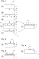
- the covering is carried out with a first thickness greater than 50 nanometers.
- the base 1 is covered by a dry route with at least a first layer 2 of sacrificial metallic protection. More particularly, the first covering is carried out by the dry route by PVD OR CVD OR ALD deposition under vacuum.
- the base 1 is electrolytically or electrochemically covered with at least a first layer 2 of sacrificial metallic protection.
- the covering is carried out with a second thickness of between 50 nanometers and 1,000 nanometers.
- the base 1 is covered by a dry route with at least a second layer 4 of metallic decorative treatment or / and of colored decorative treatment. More particularly, the second coating operation 400 is carried out by the dry route by PVD OR CVD OR ALD deposition under vacuum.
- the base 1 is electrolytically or electrochemically covered with at least one second layer 4 of metallic decorative treatment or / and of colored decorative treatment.
- the etching is carried out everywhere up to the substrate of the base 1.
- the first covering is carried out with a first thickness which is greater than or equal to the difference between, on the one hand, a second thickness of a second layer 4 of metallic decorative treatment or / and colored to be applied during step 400 of covering the first recessed decoration 3 and the remaining part of the first sacrificial metallic protective layer 2, and on the other hand the depth of etching in the substrate of the base 1 during of the engraving operation 300 of a first hollow decoration 3.
- the etching is carried out in the form of a juxtaposition of conical or deep pyramidal cups.
- the etching is carried out with a depth in the base 1 of between 20 nanometers and the total thickness of the base 1.
- the covering is carried out at least partially by the dry process, or entirely by dry process, with superposition of several first layers 2, 21, 22, of different nature.
- the covering is carried out at least partially by electrolytic or electrochemical means, or entirely by electrolytic or electrochemical means, with superposition of several first layers 2, 21, 22, of the type different.
- the deposition of certain layers is carried out by the dry route, and of certain other layers by the electrolytic or electrochemical route.
- step 400 of covering the hollow decoration 3 and the remaining part of said first layer 2 of sacrificial metallic protection, by at least one second layer 4 of metallic or / and colored decorative treatment the covering is carried out with superposition of several second layers 4 of different nature, 41, 42.
- the covering is carried out at least partially by the dry route, or entirely by the dry route, with superposition of several second layers 4, 41, 42, of a different nature.
- the covering is carried out at least partially electrolytically or electrochemically, or entirely by electrolytic or electrochemical route, with superposition of several second layers 4, 41, 42, of a type different.
- the deposition of certain layers is carried out by the dry route, and of certain other layers by the electrolytic or electrochemical route.
- a plurality of second layers 4, 41, 42 are superposed with at least one chromium layer 41 of 50 to 250 nanometers and a gold layer 42 of 50 to 150 nanometers. More particularly, the deposition is carried out by superimposing a layer of chromium approximately 200 nanometers thick, and a layer of gold approximately 100 nanometers thick.
- the figure 1 shows a variant 410, less easy to perform, where the operation 400 is modified by depositing the second decorative treatment layer flush with the first layer 2 of sacrificial metallic protection.
- a metallic sacrificial protective layer avoids degassing.
- P 1.10 -8 mbar
- temperature typically T ⁇ 300 ° C
- cleaning is carried out: detergent and / or solvent, with / without ultrasound, with / without stress. mechanical, with / without temperature, to ensure the cleanliness of the surface and thus ensure the good grip of the sacrificial metal protection.
- the etching is carried out everywhere in the substrate of the base 1, as visible on the figure. figure 2 .
- the blank should be cleaned after the etching operation, before proceeding with the second decorative treatment deposit, in particular by PVD OR CVD OR ALD.
- This cleaning is conventional (detergent and / or solvent, with / without ultrasound, with / without mechanical stress, with / without temperature), but it must not alter the sacrificial metallic protection.
- the sacrificial metallic protection comprises aluminum, it is necessary to exclude washing solutions having a too basic pH.
- step 500 before or after the chemical elimination (in step 500) of each first layer 2 of sacrificial metallic protection, the compound thus produced is mechanically leveled (in a step 550) at the upper level of the invention. 'base 1.
- the compound thus produced at the upper level of the first layer 2 of sacrificial metallic protection is mechanically leveled in a step 450.
- the compound thus produced is mechanically leveled in step 550 at the upper level of the base 1.
- the compound thus produced is mechanically leveled in step 550 at the upper level of the base 1.
- this covering is carried out by the dry route by PVD OR CVD OR ALD deposition under vacuum; different methods may also be suitable: vacuum evaporation, vacuum spraying, PECVD, or others. In another variant, this covering is carried out electrolytically or electrochemically.
- this covering is carried out with a first thickness greater than 50 nanometers.
- step 400 of covering the hollow decoration 3 and the remaining part of the first layer 2 of sacrificial metallic protection, with at least one second layer 4 of metallic or / and colored decorative treatment can be carried out by the dry route, in particular by PVD deposition under vacuum (different methods may be suitable: evaporation under vacuum, spraying under vacuum, CVD, ALD or others), or else by electrolytic or electrochemical route.
- the step 400 of covering the hollow decoration 3 and the remaining part of the first layer 2 of sacrificial metallic protection, by at least a second layer 4 of metallic or / and colored decorative treatment this is carried out.
- covering with a second thickness between 50 nanometers and 2000 nanometers, more particularly between 50 nanometers and 1000 nanometers.
- the covering is carried out with a first thickness which is greater than or equal to the difference between, on the one hand, a second thickness of a second layer 4 of metallic or / and colored decorative treatment during step 400 of covering the hollow decoration 3 and of the remaining part of said first layer 2 of metallic protection sacrificial, and on the other hand the depth of etching in the substrate of the base 1 during the etching operation 30 of a hollow decoration 3.
- the etching is carried out mechanically or by means of a laser, in particular nano-, pico- or femto-laser.
- step 300 of etching a hollow decoration 3, with a depth at least equal to the local thickness of the first layer 2 of sacrificial metallic protection the etching is carried out in the form of a juxtaposition of deep conical or pyramidal bowls.
- this etching 300 is carried out with a depth in the base 1 of between 20 nanometers and the total thickness of the base 1. It is thus possible, for example, to hollow out a very deep conical bowl over the entire thickness. of a dial, for example with a thickness of the order of a millimeter.
- a laser engraving substantially flat, approximately 20 ⁇ m deep is carried out.
- a deeper laser engraving is carried out, for example to define a cuvette, or even a bevelled date window, or the like.
- the invention allows the very fine production of such a two-tone beveled window, excessively difficult to achieve by other means.
- the covering is carried out with superposition of several first layers 2 of different nature 21, 22.
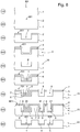
- the first blank 10 is covered by a galvanic process with at least one surface layer 7 of the first sacrificial metallic protective material or d another sacrificial metallic shielding material.
- the galvanic process however needs to be applied to a conductive substrate.
- the first blank 10 of at least one is covered by the dry route, more particularly by PVD, CVD, ALD deposition, or the like.
- third layer 6 of the first sacrificial metallic shielding material, or of another sacrificial metallic shielding material. This method of covering is independent of the nature of the substrate.
- the third layer 6 is then covered by a galvanic process with at least one surface layer 7 of the first metallic protective material. sacrificial, or sacrificial metallic shielding material of the third layer 6, or another sacrificial metallic shielding material.
- the choice of a third conductive layer 6 allows the application of the galvanic process for constituting the surface layer 7. None prevents the material of the third layer 6 from being the same as that of the surface layer 7, for example of copper.
- a second engraving operation 700 is carried out in which the engraving of a second decoration is carried out, mechanically or by means of a laser. recessed 8, with a depth at least equal to the cumulative thickness of the layers deposited during the third covering operation 600, on the first blank 10, to produce a second intermediate compound 15.
- a fourth covering operation 800 is carried out, during which the second recessed decoration 8 and the outermost surface of the second intermediate compound 15 are covered with at least a fifth layer 9 of a fifth material for metallic decorative treatment or / and colored decorative treatment, to obtain a third intermediate compound 16.
- a second chemical removal operation 900 is carried out, by which each sacrificial metallic protective layer is chemically removed, in order to obtain a second blank 20 comprising the first decoration formed by the remaining part of the second layer 4, and a second decoration formed by the remaining part of the fifth layer 9, and the watch component is produced either directly in the form of this second blank 20, or by a completion of this second blank 20.
- At least one sixth material for metallic decorative treatment or / and colored decorative treatment is chosen, and it is repeated, for the production of the blank, with the same sacrificial metallic protection materials or other protective materials.
- analogous sacrificial metal the sequence combining the third covering operation 600, the second etching operation 700, the fourth covering operation 800, and the second chemical removal operation 900, for the production of at least one other decoration added to the first decor and the second decor.
- an intermediate etching operation 810 is carried out during which the etching of an etching is carried out, mechanically or by means of a laser.
- third hollow decoration 81 is carried out after the fourth covering operation 800 and before the second chemical removal operation 900.
- a mechanical leveling operation 550 or 910 is carried out, during which the compound thus produced is mechanically leveled off at the upper level 101 of the. base 1, or below this upper level 101, to achieve an appearance surface at the upper level 411 of the remaining part of the component. More particularly, after the completion of the first elementary cycle and a cleaning, at least one other elementary cycle is carried out with parameters modified for the engraving operation and / or for the choice of the decorative treatment.
- the invention lends itself particularly well to the preferred case where, during the production step 100 of the base 1, a ceramic substrate is used.
- At least one sacrificial metallic protective material is used which is copper or aluminum or gold or platinum.
- the watch component is manufactured to form a covering element or a dial.
- the method according to the invention is well suited to the manufacture of a covering element such as a box, a bezel, a flange, or a watch or jewelry dial, or else of a jewelry component, for example a bracelet or jewelry element, made of a conductive material, in particular ceramic or the like, making it possible to obtain metallic and / or colored engraved decorations.
- a covering element such as a box, a bezel, a flange, or a watch or jewelry dial
- a jewelry component for example a bracelet or jewelry element, made of a conductive material, in particular ceramic or the like, making it possible to obtain metallic and / or colored engraved decorations.
- the invention makes it possible to produce two-color or multi-color components.
- At least one other elementary cycle can be carried out with parameters modified for the etching operation and / or for the choice of decorative treatment.
- This cycle can be repeated several times to obtain multicolored components, for example having parts of different appearance in Au, Ti, Si, Rh, or others.
- a particular texture of the engraving can also make it possible to obtain a particular visual appearance, depending on the roughness, the density and the depth of the engraving, which determine the reflections or a particular rendering of the decorative treatment applied, for example satin, semi-gloss. mat, shiny, or other.
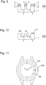
- the invention also relates to a watch 1000, which comprises a covering element 110, such as a bezel, case, or the like, in particular in ceramic, or / and which comprises a dial 120, in particular in ceramic, produced by the method according to l 'invention.
- a covering element 110 such as a bezel, case, or the like
- a dial 120 in particular in ceramic, produced by the method according to l 'invention.
- the use of a metallic sacrificial protective layer makes it possible to avoid any problematic degassing during the preferred vacuum treatment for the application of the metallic and / or colored decorative treatment layer.
- the invention lends itself well to the decoration of conductive dials (ceramic, enamel, sapphire, plastic, or other), crystals (glass, sapphire, or other), plastic components, watch cases, middle parts, glasses. , crowns, and more.
- conductive dials ceramic, enamel, sapphire, plastic, or other
- crystals glass, sapphire, or other
- plastic components watch cases, middle parts, glasses. , crowns, and more.
- the quality, finesse and contrast of the decorations which can be made in precious metals, allow a decoration of great finesse compatible with luxury watchmaking, and in particular the decoration of complication elements, such as phase indicators, for example. moonlight at high resolution.
- the reasonable cost of the implementation of the method also allows its use for components of watches or jewelry of wider distribution.
- the invention is advantageous, not only for watch components or jewelry, but also for jewelry or components of jewelry, even eyewear or fashion items.
- the invention makes it possible to modify and significantly enrich the appearance of components directly visible to the user, with innovative decorations, and participate in the promotion of the brand and the product. More particularly, the invention can be used for identification markings and / or anti-counterfeiting markings.
Landscapes
- Physics & Mathematics (AREA)
- General Physics & Mathematics (AREA)
- Engineering & Computer Science (AREA)
- Chemical & Material Sciences (AREA)
- Manufacturing & Machinery (AREA)
- Materials Engineering (AREA)
- Mechanical Engineering (AREA)
- Optics & Photonics (AREA)
- Chemical Kinetics & Catalysis (AREA)
- Metallurgy (AREA)
- Organic Chemistry (AREA)
- Plasma & Fusion (AREA)
- Electrochemistry (AREA)
- Health & Medical Sciences (AREA)
- General Health & Medical Sciences (AREA)
- Toxicology (AREA)
- Other Surface Treatments For Metallic Materials (AREA)
- Manufacture Of Switches (AREA)
- ing And Chemical Polishing (AREA)
- Physical Vapour Deposition (AREA)
- Laminated Bodies (AREA)
- Laser Beam Processing (AREA)
- Surface Heating Bodies (AREA)
Priority Applications (8)
| Application Number | Priority Date | Filing Date | Title |
|---|---|---|---|
| EP19162928.6A EP3708384A1 (de) | 2019-03-14 | 2019-03-14 | Verkleidungselement oder zifferblatt einer uhr oder eines schmuckstücks aus leitendem material |
| TW109105615A TWI777135B (zh) | 2019-03-14 | 2020-02-21 | 用於製造由導電材料製成的時計構件的方法及包含此時計構件的手錶 |
| JP2020038440A JP7005667B2 (ja) | 2019-03-14 | 2020-03-06 | 導電性材料で作られた計時器又は装飾品用の外側要素又は表盤 |
| KR1020200030639A KR20200110625A (ko) | 2019-03-14 | 2020-03-12 | 전도성 재료로 이루어진 쥬얼리 또는 시계학을 위한 외부 엘리먼트 또는 다이얼 |
| RU2020110364A RU2743680C1 (ru) | 2019-03-14 | 2020-03-12 | Внешний элемент или циферблат для часов или ювелирных изделий, выполненный из проводящего материала |
| US16/816,309 US11977356B2 (en) | 2019-03-14 | 2020-03-12 | External element or dial for horology or jewellery made of conductive material |
| CN202010175951.8A CN111694261A (zh) | 2019-03-14 | 2020-03-13 | 导电材料制成的用于钟表或珠宝的外部元件或表盘 |
| KR1020210175063A KR102523685B1 (ko) | 2019-03-14 | 2021-12-08 | 전도성 재료로 이루어진 쥬얼리 또는 시계학을 위한 외부 엘리먼트 또는 다이얼 |
Applications Claiming Priority (1)
| Application Number | Priority Date | Filing Date | Title |
|---|---|---|---|
| EP19162928.6A EP3708384A1 (de) | 2019-03-14 | 2019-03-14 | Verkleidungselement oder zifferblatt einer uhr oder eines schmuckstücks aus leitendem material |
Publications (1)
| Publication Number | Publication Date |
|---|---|
| EP3708384A1 true EP3708384A1 (de) | 2020-09-16 |
Family
ID=65817804
Family Applications (1)
| Application Number | Title | Priority Date | Filing Date |
|---|---|---|---|
| EP19162928.6A Pending EP3708384A1 (de) | 2019-03-14 | 2019-03-14 | Verkleidungselement oder zifferblatt einer uhr oder eines schmuckstücks aus leitendem material |
Country Status (7)
| Country | Link |
|---|---|
| US (1) | US11977356B2 (de) |
| EP (1) | EP3708384A1 (de) |
| JP (1) | JP7005667B2 (de) |
| KR (2) | KR20200110625A (de) |
| CN (1) | CN111694261A (de) |
| RU (1) | RU2743680C1 (de) |
| TW (1) | TWI777135B (de) |
Cited By (2)
| Publication number | Priority date | Publication date | Assignee | Title |
|---|---|---|---|---|
| EP4327690A1 (de) * | 2022-08-22 | 2024-02-28 | Comadur S.A. | Verkleidungsbauteil einer uhr oder eines mode-, schmuck- oder schmuckartikels und verfahren zur herstellung eines solchen verkleidungsbauteils |
| EP4338638A1 (de) * | 2022-09-16 | 2024-03-20 | Comadur S.A. | Verfahren zur herstellung eines verkleidungsbauteils einer uhr, eines modeartikels oder eines schmuck- oder schmuckartikels |
Families Citing this family (5)
| Publication number | Priority date | Publication date | Assignee | Title |
|---|---|---|---|---|
| JP7052830B2 (ja) * | 2020-06-30 | 2022-04-12 | セイコーエプソン株式会社 | 時計用文字板の製造方法、時計用文字板、時計 |
| JP7497670B2 (ja) * | 2020-10-29 | 2024-06-11 | セイコーエプソン株式会社 | 時計部品の製造方法、及び時計部品 |
| US20240261867A1 (en) * | 2021-05-31 | 2024-08-08 | Petitpierre Sa | Machine tool for machining a micromechanical component, and machining method implemented by said machine tool |
| EP4206826A1 (de) * | 2021-12-30 | 2023-07-05 | Rubattel et Weyermann S.A. | Verfahren zur herstellung von appliken auf einem zifferblatt |
| CN115503383A (zh) * | 2022-09-29 | 2022-12-23 | 黄向文 | 一种外表面具有掐丝图文结构的物品及其加工方法 |
Citations (6)
| Publication number | Priority date | Publication date | Assignee | Title |
|---|---|---|---|---|
| JPH04136188A (ja) * | 1990-09-26 | 1992-05-11 | Seiko Epson Corp | 装飾部材の製造方法 |
| JPH04160154A (ja) * | 1990-10-24 | 1992-06-03 | Seiko Epson Corp | 装飾部材の製造方法 |
| JPH05156425A (ja) | 1991-12-03 | 1993-06-22 | Seiko Epson Corp | 装飾部材およびその製造方法 |
| EP3067220A1 (de) | 2015-03-13 | 2016-09-14 | Rolex Sa | Dekorationsverfahren eines uhrelements, und anhand eines solchen verfahrens hergestelltes uhrelement |
| EP3181006A1 (de) * | 2015-12-18 | 2017-06-21 | The Swatch Group Research and Development Ltd. | Verkleidungselement aus zirkon mit selektiver farbgebung |
| EP3336614A1 (de) * | 2016-12-16 | 2018-06-20 | Rubattel et Weyermann S.A. | Verkleidungselement oder zifferblatt einer uhr aus nicht-leitendem material |
Family Cites Families (17)
| Publication number | Priority date | Publication date | Assignee | Title |
|---|---|---|---|---|
| GB1525609A (en) * | 1975-12-04 | 1978-09-20 | Suisse Horlogerie | Watch case and method of manufacture thereof |
| JPH0765194B2 (ja) * | 1990-06-04 | 1995-07-12 | 東芝タンガロイ株式会社 | 有色表面物品及びその製造方法 |
| DE69112277T2 (de) * | 1990-05-31 | 1996-03-07 | Toshiba Tungaloy Co Ltd | Mehrfarbiges Produkt und Verfahren zur Herstellung desselben. |
| JPH04154988A (ja) * | 1990-10-16 | 1992-05-27 | Seiko Epson Corp | 装飾部材の製造方法 |
| JP3557868B2 (ja) | 1997-01-14 | 2004-08-25 | セイコーエプソン株式会社 | 装飾品の表面処理方法、装飾品および電子機器 |
| JP3477067B2 (ja) | 1998-03-09 | 2003-12-10 | セイコーエプソン株式会社 | 金属部材の表面処理方法および金属部材 |
| JP4160154B2 (ja) * | 1998-04-15 | 2008-10-01 | 共同印刷株式会社 | 商品販売棚用陳列トレー |
| KR100854427B1 (ko) * | 2000-11-01 | 2008-08-27 | 시티즌 세이미츠 가부시키가이샤 | 시계용 문자판 및 그 제조 방법 |
| JP4592946B2 (ja) * | 2000-12-26 | 2010-12-08 | シチズンホールディングス株式会社 | 装飾文字板 |
| JP2003222686A (ja) * | 2002-01-29 | 2003-08-08 | Seiko Epson Corp | 時 計 |
| JP5156425B2 (ja) * | 2008-02-12 | 2013-03-06 | 三洋電機株式会社 | 断熱パネル |
| EP2383244A1 (de) | 2010-04-23 | 2011-11-02 | Omega SA | Keramikelement mit mindestens einem Metalldekoreinsatz |
| WO2013135703A1 (fr) * | 2012-03-12 | 2013-09-19 | Rolex S.A. | Procédé de gravage d'un élément d'horlogerie et élément d'horlogerie obtenu par un tel procédé |
| EP2855400B1 (de) * | 2012-05-30 | 2016-06-01 | The Swatch Group Research and Development Ltd. | Keramikelement mit mindestens einem verbundkeramikdekoreinsatz |
| EP3126914B1 (de) * | 2014-04-04 | 2020-05-06 | Rolex Sa | Verfahren zur herstellung einer uhrenkomponente mit einem einsatz aus einem verbundmaterial und zugehörige uhrenkomponente und uhr |
| CH711958A2 (fr) | 2015-12-18 | 2017-06-30 | Swatch Group Res & Dev Ltd | Elément d'habillage en zircone à coloration sélective. |
| FR3059792B1 (fr) * | 2016-12-01 | 2019-05-24 | Lvmh Swiss Manufactures Sa | Dispositif pour piece d'horlogerie, mouvement horloger et piece d'horlogerie comprenant un tel dispositif |
-
2019
- 2019-03-14 EP EP19162928.6A patent/EP3708384A1/de active Pending
-
2020
- 2020-02-21 TW TW109105615A patent/TWI777135B/zh active
- 2020-03-06 JP JP2020038440A patent/JP7005667B2/ja active Active
- 2020-03-12 US US16/816,309 patent/US11977356B2/en active Active
- 2020-03-12 KR KR1020200030639A patent/KR20200110625A/ko not_active Application Discontinuation
- 2020-03-12 RU RU2020110364A patent/RU2743680C1/ru active
- 2020-03-13 CN CN202010175951.8A patent/CN111694261A/zh active Pending
-
2021
- 2021-12-08 KR KR1020210175063A patent/KR102523685B1/ko active IP Right Grant
Patent Citations (6)
| Publication number | Priority date | Publication date | Assignee | Title |
|---|---|---|---|---|
| JPH04136188A (ja) * | 1990-09-26 | 1992-05-11 | Seiko Epson Corp | 装飾部材の製造方法 |
| JPH04160154A (ja) * | 1990-10-24 | 1992-06-03 | Seiko Epson Corp | 装飾部材の製造方法 |
| JPH05156425A (ja) | 1991-12-03 | 1993-06-22 | Seiko Epson Corp | 装飾部材およびその製造方法 |
| EP3067220A1 (de) | 2015-03-13 | 2016-09-14 | Rolex Sa | Dekorationsverfahren eines uhrelements, und anhand eines solchen verfahrens hergestelltes uhrelement |
| EP3181006A1 (de) * | 2015-12-18 | 2017-06-21 | The Swatch Group Research and Development Ltd. | Verkleidungselement aus zirkon mit selektiver farbgebung |
| EP3336614A1 (de) * | 2016-12-16 | 2018-06-20 | Rubattel et Weyermann S.A. | Verkleidungselement oder zifferblatt einer uhr aus nicht-leitendem material |
Cited By (2)
| Publication number | Priority date | Publication date | Assignee | Title |
|---|---|---|---|---|
| EP4327690A1 (de) * | 2022-08-22 | 2024-02-28 | Comadur S.A. | Verkleidungsbauteil einer uhr oder eines mode-, schmuck- oder schmuckartikels und verfahren zur herstellung eines solchen verkleidungsbauteils |
| EP4338638A1 (de) * | 2022-09-16 | 2024-03-20 | Comadur S.A. | Verfahren zur herstellung eines verkleidungsbauteils einer uhr, eines modeartikels oder eines schmuck- oder schmuckartikels |
Also Published As
| Publication number | Publication date |
|---|---|
| US11977356B2 (en) | 2024-05-07 |
| JP2020147849A (ja) | 2020-09-17 |
| JP7005667B2 (ja) | 2022-01-21 |
| KR20200110625A (ko) | 2020-09-24 |
| KR20210153022A (ko) | 2021-12-16 |
| CN111694261A (zh) | 2020-09-22 |
| TWI777135B (zh) | 2022-09-11 |
| TW202040295A (zh) | 2020-11-01 |
| KR102523685B1 (ko) | 2023-04-19 |
| RU2743680C1 (ru) | 2021-02-24 |
| US20200292996A1 (en) | 2020-09-17 |
Similar Documents
| Publication | Publication Date | Title |
|---|---|---|
| EP3555709B1 (de) | Verkleidungselement oder zifferblatt einer uhr aus nicht-leitendem material | |
| EP3708384A1 (de) | Verkleidungselement oder zifferblatt einer uhr oder eines schmuckstücks aus leitendem material | |
| EP2380864B1 (de) | Verfahren zur Herstellung eines Keramikelements mit mindestens einem Metalldekoreinsatz | |
| EP3709102B1 (de) | Komponente eines uhrwerks oder schmuckstücks auf keramikbasis und mit einer dekorstruktur | |
| EP3339980A1 (de) | Verfahren zur erzeugung eines dekormotivs auf einer uhr, und entsprechende uhr | |
| TWI706237B (zh) | 在微機械時計零件上形成裝飾性表面的方法及該微機械時計零件 | |
| EP3951512B1 (de) | Verfahren zur herstellung eines werkstücks mit mindestens einem metallisierten 3d-motiv | |
| CH715925A2 (fr) | Élément d'habillage ou cadran d'horlogerie ou de bijouterie en matériau conducteur. | |
| EP2881808B1 (de) | Verfahren zur Herstellung einer Uhrkomponente | |
| EP4196853A1 (de) | Schwarze komponente und verfahren zur herstellung davon | |
| JP2946911B2 (ja) | 装飾部材の製造方法 | |
| CH717875A2 (fr) | Composant noir et son procédé de fabrication. | |
| EP3839659B1 (de) | Verfahren zur dekoration eines mechanischen bauteils | |
| JP2947208B2 (ja) | 装飾部材及びこれを用いた時計 | |
| CH720291A2 (fr) | Procédé de réalisation d'un composant d'habillage comprenant un décor complexe | |
| CH717713A2 (fr) | Procédé de fabrication d'une pièce comprenant au moins un motif métallisé en trois dimensions. | |
| EP4170434A1 (de) | Verfahren zur dekoration eines substrats | |
| CH716363B1 (fr) | Procédé de décoration d'une pièce mécanique. | |
| JPH0441679A (ja) | 有色表面物品及びその製造方法 | |
| EP1930792A2 (de) | Organ für eine Uhr |
Legal Events
| Date | Code | Title | Description |
|---|---|---|---|
| PUAI | Public reference made under article 153(3) epc to a published international application that has entered the european phase |
Free format text: ORIGINAL CODE: 0009012 |
|
| STAA | Information on the status of an ep patent application or granted ep patent |
Free format text: STATUS: THE APPLICATION HAS BEEN PUBLISHED |
|
| AK | Designated contracting states |
Kind code of ref document: A1 Designated state(s): AL AT BE BG CH CY CZ DE DK EE ES FI FR GB GR HR HU IE IS IT LI LT LU LV MC MK MT NL NO PL PT RO RS SE SI SK SM TR |
|
| AX | Request for extension of the european patent |
Extension state: BA ME |
|
| STAA | Information on the status of an ep patent application or granted ep patent |
Free format text: STATUS: REQUEST FOR EXAMINATION WAS MADE |
|
| 17P | Request for examination filed |
Effective date: 20210316 |
|
| RBV | Designated contracting states (corrected) |
Designated state(s): AL AT BE BG CH CY CZ DE DK EE ES FI FR GB GR HR HU IE IS IT LI LT LU LV MC MK MT NL NO PL PT RO RS SE SI SK SM TR |
|
| STAA | Information on the status of an ep patent application or granted ep patent |
Free format text: STATUS: EXAMINATION IS IN PROGRESS |
|
| 17Q | First examination report despatched |
Effective date: 20220714 |
|
| P01 | Opt-out of the competence of the unified patent court (upc) registered |
Effective date: 20230701 |