EP3704736B1 - Verfahren zur herstellung einer folie auf einem träger mit einer nicht ebenen oberfläche - Google Patents
Verfahren zur herstellung einer folie auf einem träger mit einer nicht ebenen oberfläche Download PDFInfo
- Publication number
- EP3704736B1 EP3704736B1 EP18795628.9A EP18795628A EP3704736B1 EP 3704736 B1 EP3704736 B1 EP 3704736B1 EP 18795628 A EP18795628 A EP 18795628A EP 3704736 B1 EP3704736 B1 EP 3704736B1
- Authority
- EP
- European Patent Office
- Prior art keywords
- support
- film
- deposition
- donor substrate
- detachment
- Prior art date
- Legal status (The legal status is an assumption and is not a legal conclusion. Google has not performed a legal analysis and makes no representation as to the accuracy of the status listed.)
- Active
Links
Images




Classifications
-
- H—ELECTRICITY
- H10—SEMICONDUCTOR DEVICES; ELECTRIC SOLID-STATE DEVICES NOT OTHERWISE PROVIDED FOR
- H10W—GENERIC PACKAGES, INTERCONNECTIONS, CONNECTORS OR OTHER CONSTRUCTIONAL DETAILS OF DEVICES COVERED BY CLASS H10
- H10W10/00—Isolation regions in semiconductor bodies between components of integrated devices
- H10W10/01—Manufacture or treatment
- H10W10/011—Manufacture or treatment of isolation regions comprising dielectric materials
- H10W10/014—Manufacture or treatment of isolation regions comprising dielectric materials using trench refilling with dielectric materials, e.g. shallow trench isolations
- H10W10/0148—Manufacture or treatment of isolation regions comprising dielectric materials using trench refilling with dielectric materials, e.g. shallow trench isolations comprising introducing impurities in side walls or bottom walls of trenches, e.g. for forming channel stoppers
-
- H—ELECTRICITY
- H10—SEMICONDUCTOR DEVICES; ELECTRIC SOLID-STATE DEVICES NOT OTHERWISE PROVIDED FOR
- H10P—GENERIC PROCESSES OR APPARATUS FOR THE MANUFACTURE OR TREATMENT OF DEVICES COVERED BY CLASS H10
- H10P90/00—Preparation of wafers not covered by a single main group of this subclass, e.g. wafer reinforcement
- H10P90/19—Preparing inhomogeneous wafers
- H10P90/1904—Preparing vertically inhomogeneous wafers
- H10P90/1906—Preparing SOI wafers
- H10P90/1914—Preparing SOI wafers using bonding
- H10P90/1916—Preparing SOI wafers using bonding with separation or delamination along an ion implanted layer, e.g. Smart-cut
-
- H—ELECTRICITY
- H10—SEMICONDUCTOR DEVICES; ELECTRIC SOLID-STATE DEVICES NOT OTHERWISE PROVIDED FOR
- H10N—ELECTRIC SOLID-STATE DEVICES NOT OTHERWISE PROVIDED FOR
- H10N30/00—Piezoelectric or electrostrictive devices
- H10N30/01—Manufacture or treatment
- H10N30/07—Forming of piezoelectric or electrostrictive parts or bodies on an electrical element or another base
- H10N30/072—Forming of piezoelectric or electrostrictive parts or bodies on an electrical element or another base by laminating or bonding of piezoelectric or electrostrictive bodies
-
- H—ELECTRICITY
- H10—SEMICONDUCTOR DEVICES; ELECTRIC SOLID-STATE DEVICES NOT OTHERWISE PROVIDED FOR
- H10N—ELECTRIC SOLID-STATE DEVICES NOT OTHERWISE PROVIDED FOR
- H10N30/00—Piezoelectric or electrostrictive devices
- H10N30/01—Manufacture or treatment
- H10N30/07—Forming of piezoelectric or electrostrictive parts or bodies on an electrical element or another base
- H10N30/072—Forming of piezoelectric or electrostrictive parts or bodies on an electrical element or another base by laminating or bonding of piezoelectric or electrostrictive bodies
- H10N30/073—Forming of piezoelectric or electrostrictive parts or bodies on an electrical element or another base by laminating or bonding of piezoelectric or electrostrictive bodies by fusion of metals or by adhesives
-
- H—ELECTRICITY
- H10—SEMICONDUCTOR DEVICES; ELECTRIC SOLID-STATE DEVICES NOT OTHERWISE PROVIDED FOR
- H10P—GENERIC PROCESSES OR APPARATUS FOR THE MANUFACTURE OR TREATMENT OF DEVICES COVERED BY CLASS H10
- H10P54/00—Cutting or separating of wafers, substrates or parts of devices
- H10P54/50—Cutting or separating of wafers, substrates or parts of devices by scoring, breaking or cleaving
- H10P54/52—Cutting or separating of wafers, substrates or parts of devices by scoring, breaking or cleaving by cleaving
-
- H—ELECTRICITY
- H10—SEMICONDUCTOR DEVICES; ELECTRIC SOLID-STATE DEVICES NOT OTHERWISE PROVIDED FOR
- H10P—GENERIC PROCESSES OR APPARATUS FOR THE MANUFACTURE OR TREATMENT OF DEVICES COVERED BY CLASS H10
- H10P90/00—Preparation of wafers not covered by a single main group of this subclass, e.g. wafer reinforcement
-
- H—ELECTRICITY
- H10—SEMICONDUCTOR DEVICES; ELECTRIC SOLID-STATE DEVICES NOT OTHERWISE PROVIDED FOR
- H10P—GENERIC PROCESSES OR APPARATUS FOR THE MANUFACTURE OR TREATMENT OF DEVICES COVERED BY CLASS H10
- H10P90/00—Preparation of wafers not covered by a single main group of this subclass, e.g. wafer reinforcement
- H10P90/24—Preparation of wafers not covered by a single main group of this subclass, e.g. wafer reinforcement by concurrent transfer of multiple parts
-
- H—ELECTRICITY
- H10—SEMICONDUCTOR DEVICES; ELECTRIC SOLID-STATE DEVICES NOT OTHERWISE PROVIDED FOR
- H10W—GENERIC PACKAGES, INTERCONNECTIONS, CONNECTORS OR OTHER CONSTRUCTIONAL DETAILS OF DEVICES COVERED BY CLASS H10
- H10W10/00—Isolation regions in semiconductor bodies between components of integrated devices
- H10W10/10—Isolation regions comprising dielectric materials
- H10W10/181—Semiconductor-on-insulator [SOI] isolation regions, e.g. buried oxide regions of SOI wafers
-
- H—ELECTRICITY
- H10—SEMICONDUCTOR DEVICES; ELECTRIC SOLID-STATE DEVICES NOT OTHERWISE PROVIDED FOR
- H10P—GENERIC PROCESSES OR APPARATUS FOR THE MANUFACTURE OR TREATMENT OF DEVICES COVERED BY CLASS H10
- H10P90/00—Preparation of wafers not covered by a single main group of this subclass, e.g. wafer reinforcement
- H10P90/19—Preparing inhomogeneous wafers
- H10P90/1904—Preparing vertically inhomogeneous wafers
- H10P90/1906—Preparing SOI wafers
-
- H—ELECTRICITY
- H10—SEMICONDUCTOR DEVICES; ELECTRIC SOLID-STATE DEVICES NOT OTHERWISE PROVIDED FOR
- H10W—GENERIC PACKAGES, INTERCONNECTIONS, CONNECTORS OR OTHER CONSTRUCTIONAL DETAILS OF DEVICES COVERED BY CLASS H10
- H10W10/00—Isolation regions in semiconductor bodies between components of integrated devices
- H10W10/01—Manufacture or treatment
- H10W10/011—Manufacture or treatment of isolation regions comprising dielectric materials
- H10W10/014—Manufacture or treatment of isolation regions comprising dielectric materials using trench refilling with dielectric materials, e.g. shallow trench isolations
-
- H—ELECTRICITY
- H10—SEMICONDUCTOR DEVICES; ELECTRIC SOLID-STATE DEVICES NOT OTHERWISE PROVIDED FOR
- H10W—GENERIC PACKAGES, INTERCONNECTIONS, CONNECTORS OR OTHER CONSTRUCTIONAL DETAILS OF DEVICES COVERED BY CLASS H10
- H10W10/00—Isolation regions in semiconductor bodies between components of integrated devices
- H10W10/01—Manufacture or treatment
- H10W10/061—Manufacture or treatment using SOI processes together with lateral isolation, e.g. combinations of SOI and shallow trench isolations
-
- H—ELECTRICITY
- H10—SEMICONDUCTOR DEVICES; ELECTRIC SOLID-STATE DEVICES NOT OTHERWISE PROVIDED FOR
- H10W—GENERIC PACKAGES, INTERCONNECTIONS, CONNECTORS OR OTHER CONSTRUCTIONAL DETAILS OF DEVICES COVERED BY CLASS H10
- H10W10/00—Isolation regions in semiconductor bodies between components of integrated devices
- H10W10/10—Isolation regions comprising dielectric materials
- H10W10/17—Isolation regions comprising dielectric materials formed using trench refilling with dielectric materials, e.g. shallow trench isolations
Definitions
- the donor substrate may comprise a plurality of pads laid out on the surface of a wafer, each pad comprising an embrittlement zone delimiting a respective film to transfer, and the support is deposited on the surface of the whole of said pads.
- the deposition of the support may include the successive deposition of at least two layers of different materials.
- An intermediate structure may be obtained after deposition of the support on the donor substrate.
- Said structure comprises:
- the invention provides for the formation of the support by deposition on a non-flat donor substrate that has been embrittled beforehand so as to delimit a thin film. Said thin film is next transferred onto the support by detachment of the donor substrate.
- the support may be constituted of a single material or a stack of at least two different materials, deposited successively on the donor substrate.
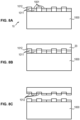
- a support 20 is formed on the surface of the film 12 which, at this stage, still forms part of the donor substrate 10.
- an intermediate layer 21 may be deposited on the film 12 before the deposition of the support 20 (the final structure being represented in figure 1E ).
- a layer may notably have the function of avoiding the diffusion of chemical species to the film 12 during the deposition of the support 20, and/or to form an electrical contact on the film 12, and/or to form an optical index jump, and/or instead to minimise a discontinuity in acoustic impedance.
- those skilled in the art are capable of choosing the suitable material and its thickness according to the mechanical, electrical, optical, thermal, acoustic or chemical function of the intermediate layer.
- a support 20 is formed by deposition on the surface of the film 12 which, at this stage, still forms part of the donor substrate 10. As indicated previously, the deposition of the support may be preceded by the deposition of an intermediate layer (not represented).
- the donor substrate 10 is next detached along the embrittlement zone 11, so as to transfer said film 12 onto the support 20.
- a residue 10' of the donor substrate remains, which can potentially be recycled with a view to another use.
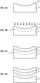
- Figures 4A to 4D show in a schematic manner another example of the transfer method not being part of the present invention, wherein the surface of the donor substrate has a textured topology.
- Said topology may notably correspond to a roughness of the surface of the donor substrate, obtained voluntarily or not.
- the surface 10a of the donor substrate 10 has a certain roughness, for example greater than or equal to 1 nm rms.
- an implantation of atomic species through the surface 10a has the effect of forming an embrittlement zone 11 within the donor substrate 10.
- the surface of the donor substrate may potentially be textured after the formation of the embrittlement zone.
- a support 20 is formed by deposition on the surface of the film 12 which, at this stage, still forms part of the donor substrate 10. As indicated previously, the deposition of the support may be preceded by the deposition of an intermediate layer (not represented).
- the deposition may be conformal, that is to say that the free surface of the support has substantially the same texture as the donor substrate, the thickness of material between the surface of the support and the surface of the donor substrate remaining substantially constant.
- the method of figures 4A to 4D is particularly interesting for acoustic wave structures such as radiofrequency (RF) filters for example, and notably to avoid reflections of parasitic waves on the rear face of the substrates and or layers considered.
- RF radiofrequency
- Helium ions are implanted in said substrate 10 so as to form an embrittlement zone 11 and delimit a thin LiNbOs film 12 (cf. figure 1B ).
- the thickness of the film 12 is of the order of 0.3 ⁇ m.
- An adhesion layer 21 constituted of a Cr/Cu alloy is deposited on the film 12 by a PVD technique.
- a copper sheet 20 is next deposited on said adhesion layer 21 by an electrochemical deposition technique (cf. figure 1E ).
- the thickness of said sheet is of the order of 20 ⁇ m.
- an annealing is applied at a temperature of 300°C, in order to cause the detachment of the donor substrate 10 along the embrittlement zone 11.
- Example 2 formation of a yttrium stabilised zirconia film on a nickel sheet
- Yttrium stabilised zirconia is generally in the form of polycrystalline ceramic, and more rarely in the form of monocrystalline substrate.
- Hydrogen ions are implanted in said substrate 10 so as to form an embrittlement zone 11 and delimit a thin YSZ film 12 (cf. figure 7C ).
- the thickness of the film 12 is of the order of 1 ⁇ m.
- An adhesion layer 21 constituted of a Cr/Cu alloy is deposited on the film 12 by a PVD technique (cf. figure 7D ).
- a nickel sheet 20 is next deposited on said adhesion layer 21 by an electrochemical deposition technique (cf. figure 7E ).
- the thickness of said sheet is of the order of 20 ⁇ m.
- the support 20 may next be etched so as to obtain the final bellows shape (cf. figure 7G ).
- This example targets acoustic wave structures such as radiofrequency (RF) filters for example.
- RF radiofrequency
- RF structures it is sought to avoid reflections of parasitic waves on the rear face of the substrates and or layers considered.
- One means consists in making geometrically imperfect the interfaces and rear surfaces notably by introducing voluntary texturings or other roughnesses. This constraint is difficult or even impossible to satisfy if the use of certain thin films of monocrystalline materials such as LiTaOs for example is envisaged, and this is so without resorting to the introduction of complex stacks of additional intermediate layers.
- a texturing of the surface 10a is created by photolithoetching (cf. figure 6B ).
- the implantation takes place before the texturing step but is could take place after as in the example illustrated in figures 4A-4D .
- the texturing is obtained by roughening by cathodic sputtering effect.
- the texturing may be obtained by a sanding of the surface of the substrate 10.
- a sheet 20 made of silica is deposited on the film 12 by a deposition technique at low temperature, typically below 100°C so as not to cause an untimely detachment along the embrittlement zone (cf. figure 6C ).
- the thickness of said sheet is of the order of 10 ⁇ m.
- the deposition technique the most suited notably in terms of temperature and desired final thickness.
- the sheet 20 may be made of metal instead of being made of silica.
- an annealing is applied at a temperature of the order of 200°C, in order to cause the detachment of the donor substrate 10 along the embrittlement zone 11 (cf. figure 6D ).
- each pad 1001 is parallel to the main surface of the wafer 1000.
- the thickness of each pad is not controlled with sufficient precision, there may exist a slight difference in thickness from one pad to the next (for example of the order of 1 or 2 ⁇ m thickness).
- the surface constituted of all of the surfaces of the pads has differences in levels, typically in the form of steps (the amplitude of these variations has been voluntarily exaggerated in figure 8A ). These different steps thus form a non-flat topology of the surface of the wafer.
- the pads are intended for the transfer of a superficial monocrystalline film onto a support final.
- an embrittlement zone 1011 is formed in each pad, before or after its putting in place on the wafer, to delimit a respective film 1012 to transfer, for example by an implantation such as described above.
Landscapes
- Engineering & Computer Science (AREA)
- Manufacturing & Machinery (AREA)
- Physical Vapour Deposition (AREA)
- Laminated Bodies (AREA)
- Liquid Deposition Of Substances Of Which Semiconductor Devices Are Composed (AREA)
Claims (18)
- Verfahren zum Herstellen eines Films (12) auf einem Träger (20), der eine Oberfläche aufweist, die mindestens ein vertieftes oder Reliefmuster zeigt, umfassend:- das Bereitstellen eines Spendersubstrats (10), das eine Oberfläche aufweist, die mindestens ein vertieftes oder Reliefmuster zeigt, das durch eine Vielzahl von Klötzen (1001) gebildet wird, die auf der Oberfläche eines Wafers (1000) angelegt sind,- das Bilden einer Versprödungszone (1011) in jedem Klotz (1001), um einen jeweiligen zu übertragenden Film zu begrenzen,- das Bilden des Trägers (20) durch Abscheiden auf der Oberfläche aller Klötze (1001),- das Ablösen des Spendersubstrats (10) entlang der Versprödungszone (1011), um jeden jeweiligen Film auf den Träger (20) zu übertragen.
- Verfahren nach Anspruch 1, das vor dem Abscheiden des Trägers (20) weiter das Abscheiden einer Zwischenschicht (21) auf der Oberfläche umfasst.
- Verfahren nach einem der Ansprüche 1 oder 2, wobei das Bilden der Versprödungszone (11) durch Implantation von ionischen Spezies in das Spendersubstrat (10) ausgeführt wird.
- Verfahren nach Anspruch 3, wobei die implantierten ionischen Spezies Wasserstoff und/oder Helium sind.
- Verfahren nach einem der Ansprüche 1 bis 4, wobei das Ablösen des Spendersubstrats (10) durch eine Wärmebehandlung bewirkt wird.
- Verfahren nach Anspruch 5, wobei das Abscheiden des Trägers (20) mit einem Wärmebudget umgesetzt wird, das kleiner ist als das der Ablöse-Wärmebehandlung.
- Verfahren nach einem der Ansprüche 1 bis 6, wobei der übertragene Film (12) aus einem Material besteht, ausgewählt aus: Halbleitermaterialien, piezoelektrischen Materialien, magnetischen Materialien und funktionellen Oxiden.
- Verfahren nach einem der Ansprüche 1 bis 7, wobei der übertragene Film (12) monokristallin ist.
- Verfahren nach einem der Ansprüche 1 bis 8, wobei die Dicke des übertragenen Films (12) im Bereich zwischen 100 nm und 10 µm, bevorzugt zwischen 100 nm und 1 µm, liegt.
- Verfahren nach einem der Ansprüche 1 bis 9, wobei der Träger (20) aus einem Material besteht, ausgewählt aus Metallen, Gläsern und Keramiken.
- Verfahren nach einem der Ansprüche 1 bis 10, wobei der Träger (20) eine Dicke im Bereich zwischen 1 und 50 µm aufweist.
- Verfahren nach einem der Ansprüche 1 bis 11, wobei das Material des Trägers (20) so ausgewählt ist, dass es eine Wärmekoeffizientendifferenz gegenüber dem Material des übertragenen Films (12) von kleiner als 5×10⁻⁶ K-1 im Absolutwert aufweist.
- Verfahren nach einem der Ansprüche 1 bis 12, wobei das Abscheiden des Trägers (20) über eine der folgenden Techniken umgesetzt wird: physikalische Gasphasenabscheidung, chemische Gasphasenabscheidung, elektrochemische Abscheidung, Schleuderbeschichtung, Lackieren und Sprühen.
- Verfahren nach einem der Ansprüche 1 bis 13, wobei die Oberfläche des zu übertragenden Films (12) nach dem Bilden der Versprödungszone (11) erhalten wird.
- Verfahren nach einem der Ansprüche 1 bis 13, wobei die Oberfläche des zu übertragenden Films (12) vor dem Bilden der Versprödungszone (11) erhalten wird.
- Verfahren nach Anspruch 15, wobei der Rest (10') des Spendersubstrats am Ende des Ablösens im Hinblick auf die Umsetzung eines neuen Films (12), der eine Oberfläche aufweist, die mindestens ein vertieftes oder Reliefmuster auf einem Träger (20) zeigt, recycelt wird, und der Rest des Spendersubstrats vor dem Recyceln einem Regeneriervorgang seiner Oberfläche unterzogen wird, der ein Entfernen von Material einschließt, das im Wesentlichen Null ist oder sich der Topologie des Rests (10') anpasst.
- Verfahren nach einem der Ansprüche 1 bis 16, wobei das Abscheiden des Trägers (20) das aufeinanderfolgende Abscheiden von mindestens zwei Schichten aus unterschiedlichen Materialien beinhaltet.
- Verfahren nach einem der Ansprüche 1 bis 17, das nach dem Ablösen des Spendersubstrats weiter das Abscheiden eines zusätzlichen Films (13) auf der dem Träger (20) gegenüberliegenden Seite des übertragenen Films (12) umfasst.
Priority Applications (1)
| Application Number | Priority Date | Filing Date | Title |
|---|---|---|---|
| EP24186129.3A EP4415508A3 (de) | 2017-10-31 | 2018-10-31 | Verfahren zur herstellung einer folie auf einem träger mit nichtflacher oberfläche |
Applications Claiming Priority (2)
| Application Number | Priority Date | Filing Date | Title |
|---|---|---|---|
| FR1760270A FR3073082B1 (fr) | 2017-10-31 | 2017-10-31 | Procede de fabrication d'un film sur un support presentant une surface non plane |
| PCT/EP2018/079797 WO2019086504A1 (en) | 2017-10-31 | 2018-10-31 | Method for manufacturing a film on a support having a non-flat surface |
Related Child Applications (1)
| Application Number | Title | Priority Date | Filing Date |
|---|---|---|---|
| EP24186129.3A Division EP4415508A3 (de) | 2017-10-31 | 2018-10-31 | Verfahren zur herstellung einer folie auf einem träger mit nichtflacher oberfläche |
Publications (2)
| Publication Number | Publication Date |
|---|---|
| EP3704736A1 EP3704736A1 (de) | 2020-09-09 |
| EP3704736B1 true EP3704736B1 (de) | 2024-07-03 |
Family
ID=61224009
Family Applications (2)
| Application Number | Title | Priority Date | Filing Date |
|---|---|---|---|
| EP24186129.3A Pending EP4415508A3 (de) | 2017-10-31 | 2018-10-31 | Verfahren zur herstellung einer folie auf einem träger mit nichtflacher oberfläche |
| EP18795628.9A Active EP3704736B1 (de) | 2017-10-31 | 2018-10-31 | Verfahren zur herstellung einer folie auf einem träger mit einer nicht ebenen oberfläche |
Family Applications Before (1)
| Application Number | Title | Priority Date | Filing Date |
|---|---|---|---|
| EP24186129.3A Pending EP4415508A3 (de) | 2017-10-31 | 2018-10-31 | Verfahren zur herstellung einer folie auf einem träger mit nichtflacher oberfläche |
Country Status (11)
| Country | Link |
|---|---|
| US (3) | US11373897B2 (de) |
| EP (2) | EP4415508A3 (de) |
| JP (1) | JP7266593B2 (de) |
| KR (2) | KR20240140182A (de) |
| CN (2) | CN111295743A (de) |
| ES (1) | ES2986339T3 (de) |
| FR (1) | FR3073082B1 (de) |
| PT (1) | PT3704736T (de) |
| SG (1) | SG11202003709YA (de) |
| TW (1) | TWI781244B (de) |
| WO (1) | WO2019086504A1 (de) |
Families Citing this family (6)
| Publication number | Priority date | Publication date | Assignee | Title |
|---|---|---|---|---|
| FR3063176A1 (fr) * | 2017-02-17 | 2018-08-24 | Soitec | Masquage d'une zone au bord d'un substrat donneur lors d'une etape d'implantation ionique |
| FR3108775B1 (fr) * | 2020-03-27 | 2022-02-18 | Soitec Silicon On Insulator | Procede de fabrication d’une structure composite comprenant une couche mince en sic monocristallin sur un substrat support en sic |
| FR3115278B1 (fr) * | 2020-10-16 | 2024-02-16 | Soitec Silicon On Insulator | Procédé de transfert d’une membrane |
| FR3143840B1 (fr) * | 2022-12-19 | 2026-01-02 | Soitec Silicon On Insulator | Procédé de fabrication de deux substrats dits pseudo-substrats donneurs comprenant chacun au moins deux pavés sur un substrat support |
| US20250096035A1 (en) * | 2023-09-20 | 2025-03-20 | Taiwan Semiconductor Manufacturing Company Limited | Film-on-insulator substrate including a pre-notched film and methods of forming the same |
| CN119019183B (zh) * | 2024-07-11 | 2025-11-21 | 山东工业陶瓷研究设计院有限公司 | 一种固体氧化物电池支撑体及功能层制备方法 |
Citations (5)
| Publication number | Priority date | Publication date | Assignee | Title |
|---|---|---|---|---|
| JPH11145481A (ja) * | 1997-11-06 | 1999-05-28 | Denso Corp | 半導体基板およびその製造方法 |
| US20050009296A1 (en) * | 2003-07-10 | 2005-01-13 | Bruno Ghyselen | Method for manufacturing a multilayer semiconductor structure that includes an irregular layer |
| US20060019476A1 (en) * | 2002-10-07 | 2006-01-26 | Chrystelle Lagahe | Method for making a detachable semiconductor substrate and for obtaining a semiconductor element |
| US20090149005A1 (en) * | 2004-11-29 | 2009-06-11 | Commissariat A L'energie Atomique | Method for making a dismountable substrate |
| FR3041364A1 (fr) * | 2015-09-18 | 2017-03-24 | Soitec Silicon On Insulator | Procede de transfert de paves monocristallins |
Family Cites Families (22)
| Publication number | Priority date | Publication date | Assignee | Title |
|---|---|---|---|---|
| DE4001399C1 (en) * | 1990-01-19 | 1991-07-25 | Kernforschungszentrum Karlsruhe Gmbh, 7500 Karlsruhe, De | Metallic microstructures - formed on substrates, by putting poly:methyl methacrylate] between moulding tool and silicon substrate |
| FR2714524B1 (fr) * | 1993-12-23 | 1996-01-26 | Commissariat Energie Atomique | Procede de realisation d'une structure en relief sur un support en materiau semiconducteur |
| JP3244097B2 (ja) * | 1994-03-10 | 2002-01-07 | 日本電信電話株式会社 | 多層構造の誘電体分離半導体基板の製造方法 |
| JP2772270B2 (ja) | 1995-11-22 | 1998-07-02 | 防衛庁技術研究本部長 | 酸化バナジウム膜の電気特性制御方法 |
| US5949108A (en) * | 1997-06-30 | 1999-09-07 | Intel Corporation | Semiconductor device with reduced capacitance |
| US20050124142A1 (en) * | 1998-12-31 | 2005-06-09 | Bower Robert W. | Transposed split of ion cut materials |
| US6380108B1 (en) * | 1999-12-21 | 2002-04-30 | North Carolina State University | Pendeoepitaxial methods of fabricating gallium nitride semiconductor layers on weak posts, and gallium nitride semiconductor structures fabricated thereby |
| US6638835B2 (en) * | 2001-12-11 | 2003-10-28 | Intel Corporation | Method for bonding and debonding films using a high-temperature polymer |
| US6562127B1 (en) | 2002-01-16 | 2003-05-13 | The United States Of America As Represented By The Secretary Of The Navy | Method of making mosaic array of thin semiconductor material of large substrates |
| JP2004247610A (ja) * | 2003-02-14 | 2004-09-02 | Canon Inc | 基板の製造方法 |
| FR2855910B1 (fr) | 2003-06-06 | 2005-07-15 | Commissariat Energie Atomique | Procede d'obtention d'une couche tres mince par amincissement par auto-portage provoque |
| TWI366218B (en) * | 2004-06-01 | 2012-06-11 | Semiconductor Energy Lab | Method for manufacturing semiconductor device |
| US7427554B2 (en) * | 2005-08-12 | 2008-09-23 | Silicon Genesis Corporation | Manufacturing strained silicon substrates using a backing material |
| FR2895391B1 (fr) * | 2005-12-27 | 2008-01-25 | Commissariat Energie Atomique | Procede d'elaboration de nanostructures ordonnees |
| US7803690B2 (en) * | 2006-06-23 | 2010-09-28 | Taiwan Semiconductor Manufacturing Company, Ltd. | Epitaxy silicon on insulator (ESOI) |
| FR2930072B1 (fr) * | 2008-04-15 | 2010-08-20 | Commissariat Energie Atomique | Procede de transfert d'une couche mince par echange protonique. |
| FR2961515B1 (fr) * | 2010-06-22 | 2012-08-24 | Commissariat Energie Atomique | Procede de realisation d'une couche mince de silicium monocristallin sur une couche de polymere |
| US8436363B2 (en) | 2011-02-03 | 2013-05-07 | Soitec | Metallic carrier for layer transfer and methods for forming the same |
| JP2012178548A (ja) * | 2011-02-03 | 2012-09-13 | Soytec | 層移転用金属キャリア及びその形成方法 |
| CN104995713A (zh) * | 2013-02-18 | 2015-10-21 | 住友电气工业株式会社 | Iii族氮化物复合衬底及其制造方法,层叠的iii族氮化物复合衬底,以及iii族氮化物半导体器件及其制造方法 |
| CN105424676B (zh) * | 2015-11-24 | 2019-03-22 | 深圳拓扑精膜科技有限公司 | 一种柔性表面增强拉曼光谱基底的制备方法及其应用 |
| CN105741980B (zh) * | 2016-04-01 | 2018-01-16 | 东南大学 | 一种表面具有微结构图案的柔性自支撑石墨烯导电薄膜及其制备方法 |
-
2017
- 2017-10-31 FR FR1760270A patent/FR3073082B1/fr active Active
-
2018
- 2018-10-31 TW TW107138587A patent/TWI781244B/zh active
- 2018-10-31 EP EP24186129.3A patent/EP4415508A3/de active Pending
- 2018-10-31 WO PCT/EP2018/079797 patent/WO2019086504A1/en not_active Ceased
- 2018-10-31 EP EP18795628.9A patent/EP3704736B1/de active Active
- 2018-10-31 KR KR1020247030559A patent/KR20240140182A/ko active Pending
- 2018-10-31 CN CN201880070872.1A patent/CN111295743A/zh active Pending
- 2018-10-31 PT PT187956289T patent/PT3704736T/pt unknown
- 2018-10-31 ES ES18795628T patent/ES2986339T3/es active Active
- 2018-10-31 US US16/759,990 patent/US11373897B2/en active Active
- 2018-10-31 KR KR1020207015316A patent/KR20200070391A/ko not_active Ceased
- 2018-10-31 JP JP2020524058A patent/JP7266593B2/ja active Active
- 2018-10-31 SG SG11202003709YA patent/SG11202003709YA/en unknown
- 2018-10-31 CN CN202411460037.2A patent/CN119400749A/zh active Pending
-
2022
- 2022-06-06 US US17/805,614 patent/US12087615B2/en active Active
-
2024
- 2024-07-31 US US18/790,146 patent/US20240395601A1/en active Pending
Patent Citations (5)
| Publication number | Priority date | Publication date | Assignee | Title |
|---|---|---|---|---|
| JPH11145481A (ja) * | 1997-11-06 | 1999-05-28 | Denso Corp | 半導体基板およびその製造方法 |
| US20060019476A1 (en) * | 2002-10-07 | 2006-01-26 | Chrystelle Lagahe | Method for making a detachable semiconductor substrate and for obtaining a semiconductor element |
| US20050009296A1 (en) * | 2003-07-10 | 2005-01-13 | Bruno Ghyselen | Method for manufacturing a multilayer semiconductor structure that includes an irregular layer |
| US20090149005A1 (en) * | 2004-11-29 | 2009-06-11 | Commissariat A L'energie Atomique | Method for making a dismountable substrate |
| FR3041364A1 (fr) * | 2015-09-18 | 2017-03-24 | Soitec Silicon On Insulator | Procede de transfert de paves monocristallins |
Also Published As
| Publication number | Publication date |
|---|---|
| US12087615B2 (en) | 2024-09-10 |
| EP4415508A3 (de) | 2024-11-27 |
| PT3704736T (pt) | 2024-08-05 |
| WO2019086504A1 (en) | 2019-05-09 |
| EP3704736A1 (de) | 2020-09-09 |
| EP4415508A2 (de) | 2024-08-14 |
| CN111295743A (zh) | 2020-06-16 |
| US11373897B2 (en) | 2022-06-28 |
| KR20240140182A (ko) | 2024-09-24 |
| FR3073082B1 (fr) | 2019-10-11 |
| JP7266593B2 (ja) | 2023-04-28 |
| US20220301923A1 (en) | 2022-09-22 |
| US20200303242A1 (en) | 2020-09-24 |
| FR3073082A1 (fr) | 2019-05-03 |
| KR20200070391A (ko) | 2020-06-17 |
| US20240395601A1 (en) | 2024-11-28 |
| JP2021501477A (ja) | 2021-01-14 |
| ES2986339T3 (es) | 2024-11-11 |
| SG11202003709YA (en) | 2020-05-28 |
| CN119400749A (zh) | 2025-02-07 |
| TWI781244B (zh) | 2022-10-21 |
| TW201924944A (zh) | 2019-07-01 |
Similar Documents
| Publication | Publication Date | Title |
|---|---|---|
| US12087615B2 (en) | Method for manufacturing a film on a support having a non-flat surface | |
| US20040224243A1 (en) | Mask, mask blank, and methods of producing these | |
| CN109166792B (zh) | 基于应力补偿制备柔性单晶薄膜的方法及柔性单晶薄膜 | |
| TW201230181A (en) | Process for cleaving a substrate | |
| US12052921B2 (en) | Method for manufacturing a film on a flexible sheet | |
| JP4855254B2 (ja) | 両面を有するドナーウェハから半導体材料の薄層を形成するための方法 | |
| KR20200136437A (ko) | 다이아몬드 또는 이리듐 재질의 단결정 층을 제조하는 방법 및 다이아몬드 또는 이리듐 재질의 단결정 층의 에피택셜 성장을 위한 기판 | |
| CN109830457B (zh) | 半导体器件及其形成方法 | |
| KR20200136431A (ko) | Lno 재질의 단결정 층을 제조하는 방법 및 lno 재질의 단결정 층의 에피택셜 성장을 위한 기판 | |
| CN115947299A (zh) | 一种表面加工工艺和半导体器件 | |
| TW201802881A (zh) | 用於製造用以形成三維單片積體電路之結構的方法 | |
| JP4650113B2 (ja) | 積層構造体、ドナー基板、および積層構造体の製造方法 | |
| TWI518759B (zh) | 暫時基材、處理方法及生產方法 | |
| KR20250023313A (ko) | 웨이퍼 프레임 연속 가공 마스크의 제조방법 및 이에 의해 제조된 웨이퍼 프레임 연속형 마스크 | |
| CN119497563A (zh) | 一种压电异质衬底、制备方法及半导体器件 |
Legal Events
| Date | Code | Title | Description |
|---|---|---|---|
| STAA | Information on the status of an ep patent application or granted ep patent |
Free format text: STATUS: UNKNOWN |
|
| STAA | Information on the status of an ep patent application or granted ep patent |
Free format text: STATUS: THE INTERNATIONAL PUBLICATION HAS BEEN MADE |
|
| PUAI | Public reference made under article 153(3) epc to a published international application that has entered the european phase |
Free format text: ORIGINAL CODE: 0009012 |
|
| STAA | Information on the status of an ep patent application or granted ep patent |
Free format text: STATUS: REQUEST FOR EXAMINATION WAS MADE |
|
| 17P | Request for examination filed |
Effective date: 20200525 |
|
| AK | Designated contracting states |
Kind code of ref document: A1 Designated state(s): AL AT BE BG CH CY CZ DE DK EE ES FI FR GB GR HR HU IE IS IT LI LT LU LV MC MK MT NL NO PL PT RO RS SE SI SK SM TR |
|
| AX | Request for extension of the european patent |
Extension state: BA ME |
|
| DAV | Request for validation of the european patent (deleted) | ||
| DAX | Request for extension of the european patent (deleted) | ||
| STAA | Information on the status of an ep patent application or granted ep patent |
Free format text: STATUS: EXAMINATION IS IN PROGRESS |
|
| 17Q | First examination report despatched |
Effective date: 20220208 |
|
| GRAP | Despatch of communication of intention to grant a patent |
Free format text: ORIGINAL CODE: EPIDOSNIGR1 |
|
| STAA | Information on the status of an ep patent application or granted ep patent |
Free format text: STATUS: GRANT OF PATENT IS INTENDED |
|
| RIC1 | Information provided on ipc code assigned before grant |
Ipc: H10N 30/073 20230101ALI20230502BHEP Ipc: H10N 30/072 20230101ALI20230502BHEP Ipc: H01L 21/762 20060101AFI20230502BHEP |
|
| INTG | Intention to grant announced |
Effective date: 20230605 |
|
| GRAJ | Information related to disapproval of communication of intention to grant by the applicant or resumption of examination proceedings by the epo deleted |
Free format text: ORIGINAL CODE: EPIDOSDIGR1 |
|
| STAA | Information on the status of an ep patent application or granted ep patent |
Free format text: STATUS: EXAMINATION IS IN PROGRESS |
|
| INTC | Intention to grant announced (deleted) | ||
| GRAP | Despatch of communication of intention to grant a patent |
Free format text: ORIGINAL CODE: EPIDOSNIGR1 |
|
| STAA | Information on the status of an ep patent application or granted ep patent |
Free format text: STATUS: GRANT OF PATENT IS INTENDED |
|
| INTG | Intention to grant announced |
Effective date: 20240126 |
|
| GRAS | Grant fee paid |
Free format text: ORIGINAL CODE: EPIDOSNIGR3 |
|
| GRAA | (expected) grant |
Free format text: ORIGINAL CODE: 0009210 |
|
| STAA | Information on the status of an ep patent application or granted ep patent |
Free format text: STATUS: THE PATENT HAS BEEN GRANTED |
|
| AK | Designated contracting states |
Kind code of ref document: B1 Designated state(s): AL AT BE BG CH CY CZ DE DK EE ES FI FR GB GR HR HU IE IS IT LI LT LU LV MC MK MT NL NO PL PT RO RS SE SI SK SM TR |
|
| REG | Reference to a national code |
Ref country code: CH Ref legal event code: EP |
|
| REG | Reference to a national code |
Ref country code: DE Ref legal event code: R096 Ref document number: 602018071343 Country of ref document: DE |
|
| REG | Reference to a national code |
Ref country code: PT Ref legal event code: SC4A Ref document number: 3704736 Country of ref document: PT Date of ref document: 20240805 Kind code of ref document: T Free format text: AVAILABILITY OF NATIONAL TRANSLATION Effective date: 20240730 |
|
| REG | Reference to a national code |
Ref country code: NL Ref legal event code: FP |
|
| REG | Reference to a national code |
Ref country code: LT Ref legal event code: MG9D |
|
| REG | Reference to a national code |
Ref country code: ES Ref legal event code: FG2A Ref document number: 2986339 Country of ref document: ES Kind code of ref document: T3 Effective date: 20241111 |
|
| REG | Reference to a national code |
Ref country code: AT Ref legal event code: MK05 Ref document number: 1700741 Country of ref document: AT Kind code of ref document: T Effective date: 20240703 |
|
| PG25 | Lapsed in a contracting state [announced via postgrant information from national office to epo] |
Ref country code: NO Free format text: LAPSE BECAUSE OF FAILURE TO SUBMIT A TRANSLATION OF THE DESCRIPTION OR TO PAY THE FEE WITHIN THE PRESCRIBED TIME-LIMIT Effective date: 20241003 |
|
| PG25 | Lapsed in a contracting state [announced via postgrant information from national office to epo] |
Ref country code: GR Free format text: LAPSE BECAUSE OF FAILURE TO SUBMIT A TRANSLATION OF THE DESCRIPTION OR TO PAY THE FEE WITHIN THE PRESCRIBED TIME-LIMIT Effective date: 20241004 Ref country code: FI Free format text: LAPSE BECAUSE OF FAILURE TO SUBMIT A TRANSLATION OF THE DESCRIPTION OR TO PAY THE FEE WITHIN THE PRESCRIBED TIME-LIMIT Effective date: 20240703 Ref country code: PL Free format text: LAPSE BECAUSE OF FAILURE TO SUBMIT A TRANSLATION OF THE DESCRIPTION OR TO PAY THE FEE WITHIN THE PRESCRIBED TIME-LIMIT Effective date: 20240703 |
|
| PG25 | Lapsed in a contracting state [announced via postgrant information from national office to epo] |
Ref country code: BG Free format text: LAPSE BECAUSE OF FAILURE TO SUBMIT A TRANSLATION OF THE DESCRIPTION OR TO PAY THE FEE WITHIN THE PRESCRIBED TIME-LIMIT Effective date: 20240703 |
|
| PG25 | Lapsed in a contracting state [announced via postgrant information from national office to epo] |
Ref country code: LV Free format text: LAPSE BECAUSE OF FAILURE TO SUBMIT A TRANSLATION OF THE DESCRIPTION OR TO PAY THE FEE WITHIN THE PRESCRIBED TIME-LIMIT Effective date: 20240703 |
|
| PG25 | Lapsed in a contracting state [announced via postgrant information from national office to epo] |
Ref country code: IS Free format text: LAPSE BECAUSE OF FAILURE TO SUBMIT A TRANSLATION OF THE DESCRIPTION OR TO PAY THE FEE WITHIN THE PRESCRIBED TIME-LIMIT Effective date: 20241103 Ref country code: AT Free format text: LAPSE BECAUSE OF FAILURE TO SUBMIT A TRANSLATION OF THE DESCRIPTION OR TO PAY THE FEE WITHIN THE PRESCRIBED TIME-LIMIT Effective date: 20240703 |
|
| PG25 | Lapsed in a contracting state [announced via postgrant information from national office to epo] |
Ref country code: HR Free format text: LAPSE BECAUSE OF FAILURE TO SUBMIT A TRANSLATION OF THE DESCRIPTION OR TO PAY THE FEE WITHIN THE PRESCRIBED TIME-LIMIT Effective date: 20240703 Ref country code: CZ Free format text: LAPSE BECAUSE OF FAILURE TO SUBMIT A TRANSLATION OF THE DESCRIPTION OR TO PAY THE FEE WITHIN THE PRESCRIBED TIME-LIMIT Effective date: 20240703 |
|
| PG25 | Lapsed in a contracting state [announced via postgrant information from national office to epo] |
Ref country code: RS Free format text: LAPSE BECAUSE OF FAILURE TO SUBMIT A TRANSLATION OF THE DESCRIPTION OR TO PAY THE FEE WITHIN THE PRESCRIBED TIME-LIMIT Effective date: 20241003 |
|
| PG25 | Lapsed in a contracting state [announced via postgrant information from national office to epo] |
Ref country code: RS Free format text: LAPSE BECAUSE OF FAILURE TO SUBMIT A TRANSLATION OF THE DESCRIPTION OR TO PAY THE FEE WITHIN THE PRESCRIBED TIME-LIMIT Effective date: 20241003 Ref country code: PL Free format text: LAPSE BECAUSE OF FAILURE TO SUBMIT A TRANSLATION OF THE DESCRIPTION OR TO PAY THE FEE WITHIN THE PRESCRIBED TIME-LIMIT Effective date: 20240703 Ref country code: NO Free format text: LAPSE BECAUSE OF FAILURE TO SUBMIT A TRANSLATION OF THE DESCRIPTION OR TO PAY THE FEE WITHIN THE PRESCRIBED TIME-LIMIT Effective date: 20241003 Ref country code: LV Free format text: LAPSE BECAUSE OF FAILURE TO SUBMIT A TRANSLATION OF THE DESCRIPTION OR TO PAY THE FEE WITHIN THE PRESCRIBED TIME-LIMIT Effective date: 20240703 Ref country code: IS Free format text: LAPSE BECAUSE OF FAILURE TO SUBMIT A TRANSLATION OF THE DESCRIPTION OR TO PAY THE FEE WITHIN THE PRESCRIBED TIME-LIMIT Effective date: 20241103 Ref country code: HR Free format text: LAPSE BECAUSE OF FAILURE TO SUBMIT A TRANSLATION OF THE DESCRIPTION OR TO PAY THE FEE WITHIN THE PRESCRIBED TIME-LIMIT Effective date: 20240703 Ref country code: GR Free format text: LAPSE BECAUSE OF FAILURE TO SUBMIT A TRANSLATION OF THE DESCRIPTION OR TO PAY THE FEE WITHIN THE PRESCRIBED TIME-LIMIT Effective date: 20241004 Ref country code: FI Free format text: LAPSE BECAUSE OF FAILURE TO SUBMIT A TRANSLATION OF THE DESCRIPTION OR TO PAY THE FEE WITHIN THE PRESCRIBED TIME-LIMIT Effective date: 20240703 Ref country code: CZ Free format text: LAPSE BECAUSE OF FAILURE TO SUBMIT A TRANSLATION OF THE DESCRIPTION OR TO PAY THE FEE WITHIN THE PRESCRIBED TIME-LIMIT Effective date: 20240703 Ref country code: BG Free format text: LAPSE BECAUSE OF FAILURE TO SUBMIT A TRANSLATION OF THE DESCRIPTION OR TO PAY THE FEE WITHIN THE PRESCRIBED TIME-LIMIT Effective date: 20240703 Ref country code: AT Free format text: LAPSE BECAUSE OF FAILURE TO SUBMIT A TRANSLATION OF THE DESCRIPTION OR TO PAY THE FEE WITHIN THE PRESCRIBED TIME-LIMIT Effective date: 20240703 |
|
| REG | Reference to a national code |
Ref country code: DE Ref legal event code: R097 Ref document number: 602018071343 Country of ref document: DE |
|
| PG25 | Lapsed in a contracting state [announced via postgrant information from national office to epo] |
Ref country code: DK Free format text: LAPSE BECAUSE OF FAILURE TO SUBMIT A TRANSLATION OF THE DESCRIPTION OR TO PAY THE FEE WITHIN THE PRESCRIBED TIME-LIMIT Effective date: 20240703 Ref country code: RO Free format text: LAPSE BECAUSE OF FAILURE TO SUBMIT A TRANSLATION OF THE DESCRIPTION OR TO PAY THE FEE WITHIN THE PRESCRIBED TIME-LIMIT Effective date: 20240703 Ref country code: SM Free format text: LAPSE BECAUSE OF FAILURE TO SUBMIT A TRANSLATION OF THE DESCRIPTION OR TO PAY THE FEE WITHIN THE PRESCRIBED TIME-LIMIT Effective date: 20240703 |
|
| PG25 | Lapsed in a contracting state [announced via postgrant information from national office to epo] |
Ref country code: EE Free format text: LAPSE BECAUSE OF FAILURE TO SUBMIT A TRANSLATION OF THE DESCRIPTION OR TO PAY THE FEE WITHIN THE PRESCRIBED TIME-LIMIT Effective date: 20240703 |
|
| PG25 | Lapsed in a contracting state [announced via postgrant information from national office to epo] |
Ref country code: SK Free format text: LAPSE BECAUSE OF FAILURE TO SUBMIT A TRANSLATION OF THE DESCRIPTION OR TO PAY THE FEE WITHIN THE PRESCRIBED TIME-LIMIT Effective date: 20240703 |
|
| PLBE | No opposition filed within time limit |
Free format text: ORIGINAL CODE: 0009261 |
|
| STAA | Information on the status of an ep patent application or granted ep patent |
Free format text: STATUS: NO OPPOSITION FILED WITHIN TIME LIMIT |
|
| REG | Reference to a national code |
Ref country code: CH Ref legal event code: PL |
|
| 26N | No opposition filed |
Effective date: 20250404 |
|
| PG25 | Lapsed in a contracting state [announced via postgrant information from national office to epo] |
Ref country code: MC Free format text: LAPSE BECAUSE OF FAILURE TO SUBMIT A TRANSLATION OF THE DESCRIPTION OR TO PAY THE FEE WITHIN THE PRESCRIBED TIME-LIMIT Effective date: 20240703 |
|
| PG25 | Lapsed in a contracting state [announced via postgrant information from national office to epo] |
Ref country code: LU Free format text: LAPSE BECAUSE OF NON-PAYMENT OF DUE FEES Effective date: 20241031 Ref country code: BE Free format text: LAPSE BECAUSE OF NON-PAYMENT OF DUE FEES Effective date: 20241031 |
|
| PG25 | Lapsed in a contracting state [announced via postgrant information from national office to epo] |
Ref country code: CH Free format text: LAPSE BECAUSE OF NON-PAYMENT OF DUE FEES Effective date: 20241031 |
|
| REG | Reference to a national code |
Ref country code: BE Ref legal event code: MM Effective date: 20241031 |
|
| PG25 | Lapsed in a contracting state [announced via postgrant information from national office to epo] |
Ref country code: SE Free format text: LAPSE BECAUSE OF FAILURE TO SUBMIT A TRANSLATION OF THE DESCRIPTION OR TO PAY THE FEE WITHIN THE PRESCRIBED TIME-LIMIT Effective date: 20240703 |
|
| PGFP | Annual fee paid to national office [announced via postgrant information from national office to epo] |
Ref country code: NL Payment date: 20250912 Year of fee payment: 8 Ref country code: IT Payment date: 20250922 Year of fee payment: 8 |
|
| PGFP | Annual fee paid to national office [announced via postgrant information from national office to epo] |
Ref country code: GB Payment date: 20250911 Year of fee payment: 8 |
|
| PGFP | Annual fee paid to national office [announced via postgrant information from national office to epo] |
Ref country code: FR Payment date: 20250908 Year of fee payment: 8 |
|
| PG25 | Lapsed in a contracting state [announced via postgrant information from national office to epo] |
Ref country code: IE Free format text: LAPSE BECAUSE OF NON-PAYMENT OF DUE FEES Effective date: 20241031 |
|
| REG | Reference to a national code |
Ref country code: DE Ref legal event code: R079 Ref document number: 602018071343 Country of ref document: DE Free format text: PREVIOUS MAIN CLASS: H01L0021762000 Ipc: H10W0010100000 |
|
| PGFP | Annual fee paid to national office [announced via postgrant information from national office to epo] |
Ref country code: PT Payment date: 20251014 Year of fee payment: 8 |
|
| PGFP | Annual fee paid to national office [announced via postgrant information from national office to epo] |
Ref country code: DE Payment date: 20250902 Year of fee payment: 8 |
|
| PGFP | Annual fee paid to national office [announced via postgrant information from national office to epo] |
Ref country code: ES Payment date: 20251105 Year of fee payment: 8 |
|
| PG25 | Lapsed in a contracting state [announced via postgrant information from national office to epo] |
Ref country code: HU Free format text: LAPSE BECAUSE OF FAILURE TO SUBMIT A TRANSLATION OF THE DESCRIPTION OR TO PAY THE FEE WITHIN THE PRESCRIBED TIME-LIMIT; INVALID AB INITIO Effective date: 20181031 |
|
| PG25 | Lapsed in a contracting state [announced via postgrant information from national office to epo] |
Ref country code: CY Free format text: LAPSE BECAUSE OF FAILURE TO SUBMIT A TRANSLATION OF THE DESCRIPTION OR TO PAY THE FEE WITHIN THE PRESCRIBED TIME-LIMIT; INVALID AB INITIO Effective date: 20181031 |