EP3703248A1 - Power conversion device and refrigeration air conditioner - Google Patents
Power conversion device and refrigeration air conditioner Download PDFInfo
- Publication number
- EP3703248A1 EP3703248A1 EP17857648.4A EP17857648A EP3703248A1 EP 3703248 A1 EP3703248 A1 EP 3703248A1 EP 17857648 A EP17857648 A EP 17857648A EP 3703248 A1 EP3703248 A1 EP 3703248A1
- Authority
- EP
- European Patent Office
- Prior art keywords
- converter
- voltage
- power
- current
- switching
- Prior art date
- Legal status (The legal status is an assumption and is not a legal conclusion. Google has not performed a legal analysis and makes no representation as to the accuracy of the status listed.)
- Withdrawn
Links
- 238000005057 refrigeration Methods 0.000 title claims description 9
- 238000006243 chemical reaction Methods 0.000 title description 10
- 230000003071 parasitic effect Effects 0.000 claims description 14
- 230000001360 synchronised effect Effects 0.000 description 31
- 230000006870 function Effects 0.000 description 22
- 230000006872 improvement Effects 0.000 description 22
- 238000000034 method Methods 0.000 description 15
- 239000003990 capacitor Substances 0.000 description 13
- 238000009499 grossing Methods 0.000 description 13
- 238000004378 air conditioning Methods 0.000 description 7
- 230000000694 effects Effects 0.000 description 6
- 230000007423 decrease Effects 0.000 description 5
- 230000004048 modification Effects 0.000 description 5
- 238000012986 modification Methods 0.000 description 5
- 238000012545 processing Methods 0.000 description 5
- 238000011084 recovery Methods 0.000 description 5
- 238000010586 diagram Methods 0.000 description 4
- 238000001514 detection method Methods 0.000 description 3
- 230000009467 reduction Effects 0.000 description 3
- 230000008859 change Effects 0.000 description 2
- 238000010438 heat treatment Methods 0.000 description 2
- 230000008569 process Effects 0.000 description 2
- 239000003507 refrigerant Substances 0.000 description 2
- 230000004888 barrier function Effects 0.000 description 1
- 238000004891 communication Methods 0.000 description 1
- 230000000295 complement effect Effects 0.000 description 1
- 238000001816 cooling Methods 0.000 description 1
- 238000007599 discharging Methods 0.000 description 1
- 238000005516 engineering process Methods 0.000 description 1
- 239000002674 ointment Substances 0.000 description 1
- 230000010349 pulsation Effects 0.000 description 1
- 230000004044 response Effects 0.000 description 1
- 230000001629 suppression Effects 0.000 description 1
- 238000012546 transfer Methods 0.000 description 1
Images





Classifications
-
- H—ELECTRICITY
- H02—GENERATION; CONVERSION OR DISTRIBUTION OF ELECTRIC POWER
- H02M—APPARATUS FOR CONVERSION BETWEEN AC AND AC, BETWEEN AC AND DC, OR BETWEEN DC AND DC, AND FOR USE WITH MAINS OR SIMILAR POWER SUPPLY SYSTEMS; CONVERSION OF DC OR AC INPUT POWER INTO SURGE OUTPUT POWER; CONTROL OR REGULATION THEREOF
- H02M1/00—Details of apparatus for conversion
- H02M1/0083—Converters characterised by their input or output configuration
- H02M1/0085—Partially controlled bridges
-
- H—ELECTRICITY
- H02—GENERATION; CONVERSION OR DISTRIBUTION OF ELECTRIC POWER
- H02M—APPARATUS FOR CONVERSION BETWEEN AC AND AC, BETWEEN AC AND DC, OR BETWEEN DC AND DC, AND FOR USE WITH MAINS OR SIMILAR POWER SUPPLY SYSTEMS; CONVERSION OF DC OR AC INPUT POWER INTO SURGE OUTPUT POWER; CONTROL OR REGULATION THEREOF
- H02M1/00—Details of apparatus for conversion
- H02M1/42—Circuits or arrangements for compensating for or adjusting power factor in converters or inverters
- H02M1/4208—Arrangements for improving power factor of AC input
- H02M1/4225—Arrangements for improving power factor of AC input using a non-isolated boost converter
-
- H—ELECTRICITY
- H02—GENERATION; CONVERSION OR DISTRIBUTION OF ELECTRIC POWER
- H02M—APPARATUS FOR CONVERSION BETWEEN AC AND AC, BETWEEN AC AND DC, OR BETWEEN DC AND DC, AND FOR USE WITH MAINS OR SIMILAR POWER SUPPLY SYSTEMS; CONVERSION OF DC OR AC INPUT POWER INTO SURGE OUTPUT POWER; CONTROL OR REGULATION THEREOF
- H02M5/00—Conversion of AC power input into AC power output, e.g. for change of voltage, for change of frequency, for change of number of phases
- H02M5/40—Conversion of AC power input into AC power output, e.g. for change of voltage, for change of frequency, for change of number of phases with intermediate conversion into DC
- H02M5/42—Conversion of AC power input into AC power output, e.g. for change of voltage, for change of frequency, for change of number of phases with intermediate conversion into DC by static converters
- H02M5/44—Conversion of AC power input into AC power output, e.g. for change of voltage, for change of frequency, for change of number of phases with intermediate conversion into DC by static converters using discharge tubes or semiconductor devices to convert the intermediate DC into AC
- H02M5/453—Conversion of AC power input into AC power output, e.g. for change of voltage, for change of frequency, for change of number of phases with intermediate conversion into DC by static converters using discharge tubes or semiconductor devices to convert the intermediate DC into AC using devices of a triode or transistor type requiring continuous application of a control signal
- H02M5/458—Conversion of AC power input into AC power output, e.g. for change of voltage, for change of frequency, for change of number of phases with intermediate conversion into DC by static converters using discharge tubes or semiconductor devices to convert the intermediate DC into AC using devices of a triode or transistor type requiring continuous application of a control signal using semiconductor devices only
-
- H—ELECTRICITY
- H02—GENERATION; CONVERSION OR DISTRIBUTION OF ELECTRIC POWER
- H02M—APPARATUS FOR CONVERSION BETWEEN AC AND AC, BETWEEN AC AND DC, OR BETWEEN DC AND DC, AND FOR USE WITH MAINS OR SIMILAR POWER SUPPLY SYSTEMS; CONVERSION OF DC OR AC INPUT POWER INTO SURGE OUTPUT POWER; CONTROL OR REGULATION THEREOF
- H02M5/00—Conversion of AC power input into AC power output, e.g. for change of voltage, for change of frequency, for change of number of phases
- H02M5/40—Conversion of AC power input into AC power output, e.g. for change of voltage, for change of frequency, for change of number of phases with intermediate conversion into DC
- H02M5/42—Conversion of AC power input into AC power output, e.g. for change of voltage, for change of frequency, for change of number of phases with intermediate conversion into DC by static converters
- H02M5/44—Conversion of AC power input into AC power output, e.g. for change of voltage, for change of frequency, for change of number of phases with intermediate conversion into DC by static converters using discharge tubes or semiconductor devices to convert the intermediate DC into AC
- H02M5/453—Conversion of AC power input into AC power output, e.g. for change of voltage, for change of frequency, for change of number of phases with intermediate conversion into DC by static converters using discharge tubes or semiconductor devices to convert the intermediate DC into AC using devices of a triode or transistor type requiring continuous application of a control signal
- H02M5/458—Conversion of AC power input into AC power output, e.g. for change of voltage, for change of frequency, for change of number of phases with intermediate conversion into DC by static converters using discharge tubes or semiconductor devices to convert the intermediate DC into AC using devices of a triode or transistor type requiring continuous application of a control signal using semiconductor devices only
- H02M5/4585—Conversion of AC power input into AC power output, e.g. for change of voltage, for change of frequency, for change of number of phases with intermediate conversion into DC by static converters using discharge tubes or semiconductor devices to convert the intermediate DC into AC using devices of a triode or transistor type requiring continuous application of a control signal using semiconductor devices only having a rectifier with controlled elements
-
- H—ELECTRICITY
- H02—GENERATION; CONVERSION OR DISTRIBUTION OF ELECTRIC POWER
- H02M—APPARATUS FOR CONVERSION BETWEEN AC AND AC, BETWEEN AC AND DC, OR BETWEEN DC AND DC, AND FOR USE WITH MAINS OR SIMILAR POWER SUPPLY SYSTEMS; CONVERSION OF DC OR AC INPUT POWER INTO SURGE OUTPUT POWER; CONTROL OR REGULATION THEREOF
- H02M7/00—Conversion of AC power input into DC power output; Conversion of DC power input into AC power output
- H02M7/42—Conversion of DC power input into AC power output without possibility of reversal
- H02M7/44—Conversion of DC power input into AC power output without possibility of reversal by static converters
- H02M7/48—Conversion of DC power input into AC power output without possibility of reversal by static converters using discharge tubes with control electrode or semiconductor devices with control electrode
- H02M7/493—Conversion of DC power input into AC power output without possibility of reversal by static converters using discharge tubes with control electrode or semiconductor devices with control electrode the static converters being arranged for operation in parallel
-
- H—ELECTRICITY
- H02—GENERATION; CONVERSION OR DISTRIBUTION OF ELECTRIC POWER
- H02M—APPARATUS FOR CONVERSION BETWEEN AC AND AC, BETWEEN AC AND DC, OR BETWEEN DC AND DC, AND FOR USE WITH MAINS OR SIMILAR POWER SUPPLY SYSTEMS; CONVERSION OF DC OR AC INPUT POWER INTO SURGE OUTPUT POWER; CONTROL OR REGULATION THEREOF
- H02M7/00—Conversion of AC power input into DC power output; Conversion of DC power input into AC power output
- H02M7/42—Conversion of DC power input into AC power output without possibility of reversal
- H02M7/44—Conversion of DC power input into AC power output without possibility of reversal by static converters
- H02M7/48—Conversion of DC power input into AC power output without possibility of reversal by static converters using discharge tubes with control electrode or semiconductor devices with control electrode
- H02M7/53—Conversion of DC power input into AC power output without possibility of reversal by static converters using discharge tubes with control electrode or semiconductor devices with control electrode using devices of a triode or transistor type requiring continuous application of a control signal
- H02M7/537—Conversion of DC power input into AC power output without possibility of reversal by static converters using discharge tubes with control electrode or semiconductor devices with control electrode using devices of a triode or transistor type requiring continuous application of a control signal using semiconductor devices only, e.g. single switched pulse inverters
- H02M7/539—Conversion of DC power input into AC power output without possibility of reversal by static converters using discharge tubes with control electrode or semiconductor devices with control electrode using devices of a triode or transistor type requiring continuous application of a control signal using semiconductor devices only, e.g. single switched pulse inverters with automatic control of output wave form or frequency
- H02M7/5395—Conversion of DC power input into AC power output without possibility of reversal by static converters using discharge tubes with control electrode or semiconductor devices with control electrode using devices of a triode or transistor type requiring continuous application of a control signal using semiconductor devices only, e.g. single switched pulse inverters with automatic control of output wave form or frequency by pulse-width modulation
-
- H—ELECTRICITY
- H02—GENERATION; CONVERSION OR DISTRIBUTION OF ELECTRIC POWER
- H02P—CONTROL OR REGULATION OF ELECTRIC MOTORS, ELECTRIC GENERATORS OR DYNAMO-ELECTRIC CONVERTERS; CONTROLLING TRANSFORMERS, REACTORS OR CHOKE COILS
- H02P21/00—Arrangements or methods for the control of electric machines by vector control, e.g. by control of field orientation
- H02P21/24—Vector control not involving the use of rotor position or rotor speed sensors
- H02P21/28—Stator flux based control
- H02P21/30—Direct torque control [DTC] or field acceleration method [FAM]
-
- H—ELECTRICITY
- H02—GENERATION; CONVERSION OR DISTRIBUTION OF ELECTRIC POWER
- H02P—CONTROL OR REGULATION OF ELECTRIC MOTORS, ELECTRIC GENERATORS OR DYNAMO-ELECTRIC CONVERTERS; CONTROLLING TRANSFORMERS, REACTORS OR CHOKE COILS
- H02P27/00—Arrangements or methods for the control of AC motors characterised by the kind of supply voltage
- H02P27/04—Arrangements or methods for the control of AC motors characterised by the kind of supply voltage using variable-frequency supply voltage, e.g. inverter or converter supply voltage
- H02P27/06—Arrangements or methods for the control of AC motors characterised by the kind of supply voltage using variable-frequency supply voltage, e.g. inverter or converter supply voltage using DC to AC converters or inverters
- H02P27/08—Arrangements or methods for the control of AC motors characterised by the kind of supply voltage using variable-frequency supply voltage, e.g. inverter or converter supply voltage using DC to AC converters or inverters with pulse width modulation
-
- H—ELECTRICITY
- H02—GENERATION; CONVERSION OR DISTRIBUTION OF ELECTRIC POWER
- H02P—CONTROL OR REGULATION OF ELECTRIC MOTORS, ELECTRIC GENERATORS OR DYNAMO-ELECTRIC CONVERTERS; CONTROLLING TRANSFORMERS, REACTORS OR CHOKE COILS
- H02P5/00—Arrangements specially adapted for regulating or controlling the speed or torque of two or more electric motors
- H02P5/74—Arrangements specially adapted for regulating or controlling the speed or torque of two or more electric motors controlling two or more AC dynamo-electric motors
-
- H—ELECTRICITY
- H02—GENERATION; CONVERSION OR DISTRIBUTION OF ELECTRIC POWER
- H02M—APPARATUS FOR CONVERSION BETWEEN AC AND AC, BETWEEN AC AND DC, OR BETWEEN DC AND DC, AND FOR USE WITH MAINS OR SIMILAR POWER SUPPLY SYSTEMS; CONVERSION OF DC OR AC INPUT POWER INTO SURGE OUTPUT POWER; CONTROL OR REGULATION THEREOF
- H02M1/00—Details of apparatus for conversion
- H02M1/0003—Details of control, feedback or regulation circuits
- H02M1/0032—Control circuits allowing low power mode operation, e.g. in standby mode
- H02M1/0035—Control circuits allowing low power mode operation, e.g. in standby mode using burst mode control
-
- H—ELECTRICITY
- H02—GENERATION; CONVERSION OR DISTRIBUTION OF ELECTRIC POWER
- H02M—APPARATUS FOR CONVERSION BETWEEN AC AND AC, BETWEEN AC AND DC, OR BETWEEN DC AND DC, AND FOR USE WITH MAINS OR SIMILAR POWER SUPPLY SYSTEMS; CONVERSION OF DC OR AC INPUT POWER INTO SURGE OUTPUT POWER; CONTROL OR REGULATION THEREOF
- H02M1/00—Details of apparatus for conversion
- H02M1/0048—Circuits or arrangements for reducing losses
- H02M1/0054—Transistor switching losses
- H02M1/0058—Transistor switching losses by employing soft switching techniques, i.e. commutation of transistors when applied voltage is zero or when current flow is zero
-
- H—ELECTRICITY
- H02—GENERATION; CONVERSION OR DISTRIBUTION OF ELECTRIC POWER
- H02M—APPARATUS FOR CONVERSION BETWEEN AC AND AC, BETWEEN AC AND DC, OR BETWEEN DC AND DC, AND FOR USE WITH MAINS OR SIMILAR POWER SUPPLY SYSTEMS; CONVERSION OF DC OR AC INPUT POWER INTO SURGE OUTPUT POWER; CONTROL OR REGULATION THEREOF
- H02M1/00—Details of apparatus for conversion
- H02M1/0067—Converter structures employing plural converter units, other than for parallel operation of the units on a single load
- H02M1/007—Plural converter units in cascade
-
- H—ELECTRICITY
- H02—GENERATION; CONVERSION OR DISTRIBUTION OF ELECTRIC POWER
- H02M—APPARATUS FOR CONVERSION BETWEEN AC AND AC, BETWEEN AC AND DC, OR BETWEEN DC AND DC, AND FOR USE WITH MAINS OR SIMILAR POWER SUPPLY SYSTEMS; CONVERSION OF DC OR AC INPUT POWER INTO SURGE OUTPUT POWER; CONTROL OR REGULATION THEREOF
- H02M1/00—Details of apparatus for conversion
- H02M1/36—Means for starting or stopping converters
-
- H—ELECTRICITY
- H02—GENERATION; CONVERSION OR DISTRIBUTION OF ELECTRIC POWER
- H02M—APPARATUS FOR CONVERSION BETWEEN AC AND AC, BETWEEN AC AND DC, OR BETWEEN DC AND DC, AND FOR USE WITH MAINS OR SIMILAR POWER SUPPLY SYSTEMS; CONVERSION OF DC OR AC INPUT POWER INTO SURGE OUTPUT POWER; CONTROL OR REGULATION THEREOF
- H02M7/00—Conversion of AC power input into DC power output; Conversion of DC power input into AC power output
- H02M7/02—Conversion of AC power input into DC power output without possibility of reversal
- H02M7/04—Conversion of AC power input into DC power output without possibility of reversal by static converters
- H02M7/12—Conversion of AC power input into DC power output without possibility of reversal by static converters using discharge tubes with control electrode or semiconductor devices with control electrode
- H02M7/21—Conversion of AC power input into DC power output without possibility of reversal by static converters using discharge tubes with control electrode or semiconductor devices with control electrode using devices of a triode or transistor type requiring continuous application of a control signal
- H02M7/217—Conversion of AC power input into DC power output without possibility of reversal by static converters using discharge tubes with control electrode or semiconductor devices with control electrode using devices of a triode or transistor type requiring continuous application of a control signal using semiconductor devices only
- H02M7/219—Conversion of AC power input into DC power output without possibility of reversal by static converters using discharge tubes with control electrode or semiconductor devices with control electrode using devices of a triode or transistor type requiring continuous application of a control signal using semiconductor devices only in a bridge configuration
- H02M7/2195—Conversion of AC power input into DC power output without possibility of reversal by static converters using discharge tubes with control electrode or semiconductor devices with control electrode using devices of a triode or transistor type requiring continuous application of a control signal using semiconductor devices only in a bridge configuration the switches being synchronously commutated at the same frequency of the AC input voltage
-
- Y—GENERAL TAGGING OF NEW TECHNOLOGICAL DEVELOPMENTS; GENERAL TAGGING OF CROSS-SECTIONAL TECHNOLOGIES SPANNING OVER SEVERAL SECTIONS OF THE IPC; TECHNICAL SUBJECTS COVERED BY FORMER USPC CROSS-REFERENCE ART COLLECTIONS [XRACs] AND DIGESTS
- Y02—TECHNOLOGIES OR APPLICATIONS FOR MITIGATION OR ADAPTATION AGAINST CLIMATE CHANGE
- Y02B—CLIMATE CHANGE MITIGATION TECHNOLOGIES RELATED TO BUILDINGS, e.g. HOUSING, HOUSE APPLIANCES OR RELATED END-USER APPLICATIONS
- Y02B70/00—Technologies for an efficient end-user side electric power management and consumption
- Y02B70/10—Technologies improving the efficiency by using switched-mode power supplies [SMPS], i.e. efficient power electronics conversion e.g. power factor correction or reduction of losses in power supplies or efficient standby modes
Definitions
- the present invention relates to a power converter and a refrigeration air conditioner.
- a converter circuit for converting a single-phase AC voltage into a DC voltage repeats, in response to an output, an operation of storing energy in a reactor by short-circuiting through the reactor and discharging the energy in the reactor during rectifying operation. According to this, the converter circuit boosts the DC voltage to have high efficiency and high output of a permanent magnetic synchronous motor.
- an inverter circuit converts the DC voltage into three-phase AC power to drive the permanent synchronous motor and performs an intermittently energization control in which switching around a current zero cross is turned off.
- the power converting circuit and the permanent magnet synchronous motor are aimed to have high efficiencies.
- the boosting operation of the converter circuit and the intermittent energization operation of the inverter are performed in accordance with the input and the output to have high efficiency of the power converter.
- a cost reduction in the power converter can be provided by driving a plurality of motors with a single microcomputer.
- the microcomputer may not able to control the converter circuit and the inverter circuit.
- PATENT DOCUMENT 1 JP 5718474
- PATENT DOCUMENT 1 disclosed only the intermittent energization operation on an inverter circuit side.
- the intermittent energization operation may be performed independently from the operation on the converter circuit side.
- the boosting operation and the intermittent energization control are performed linkingly in accordance with output conditions to reduce the operation load.
- An aspect of the present invention provides a power converter and a refrigeration air conditioner using the same to optimally perform the boosting operation of the power converter and the intermittent energization operation of the inverter in accordance with the input and the output.
- the power converter according to the present invention includes a converter capable of boosting a DC voltage by a switching operation alternately performing short-circuiting and rectification through a reactor in a power source, an inverter capable of an intermittent energization to make switching around zero cross of a motor current OFF while a DC voltage outputted by the converter is converted into three-phase AC power, and a controller for performing the boosting operation of the converter and the intermittent energization operation of the inverter interlockingly.
- a high efficiency power converter can be driven in which the boosting operation of the converter and the intermittent energization operation of the inverter are optimally performed in accordance with the input and the output.
- a power converter and a refrigeration air conditioner using the power converter to optimally perform the boosting operation of the converter and the intermittent energization operation of the inverter in accordance with the input and the output.
- Fig. 1 is a general block diagram showing a power converter 1 according to the present embodiment.
- the power converter 1 includes a converter 2 connected to a AC power source VS, an inverter 3a, and a motor 4a, an inverter 3b, and a motor 4b, and a controller 5 for integrally controlling them.
- the power converter 1 further includes a current detector 11, a smoothing capacitor C1, phase current detectors 15a, 15b.
- the power converter 1 is installed in the air conditioning device.
- the inverter 3a is referred to as "an inverter A”
- the inverter 3b is referred to as "an inverter B”.
- the converter 2 converts a power supply voltage into a DC voltage and can boost the DC voltage outputted by the switching operation performing short circuiting through a coil in the power supply and rectification alternately.
- the inverter 3a is provided to rotationally drive the motor 4a with conversion of the DC voltage into an AC voltage.
- the motor 4a is a fan motor for rotating a fan of the air conditioning device.
- the inverter 3b converts the DC voltage into AC voltages to drive the motor 4b.
- the motor 4b is a motor for a compressor to drive the compressor of the air conditioning device. Further, the inverter 3a and the inverter 3b have similar circuit configurations and drive the motors 4a 4b to rotate by the similar control.
- the controller 5 controls the converter 2 on the basis of a circuit current i s detected by the current detector 11, and a DC voltage Vd outputted by the converter 2.
- the controller 5 further controls the inverters 3a, 3b on the basis of the current information and the voltage information detected by the phase current detectors 15a, 15b.
- the controller 5 can control the converter 2 to perform a boosting operation and the inverters 3a, 3b to perform the intermittent energization operation linkingly.
- Fig. 2 is a general block diagram showing the converter 2 and the controller 5, etc.
- the converter 2 converts an AC power source Vs supplied from the AC power source VS into the DC voltage Vd to supply the DC voltage Vd to a load H (inverters, motors, etc).
- the converter 2 is connected at an input side thereof to the AC power source VS and an output side thereof is connected to the load H.
- the converter 2 includes a reactor L1, the smoothing capacitor C1, diodes D1, D2, D3, D4, MOSFETs Q1, Q2, which are switching elements, and a shunt resister R1.
- the diodes D1, D2, D3, D4 and the MOSFETs Q1, Q2 form a bridge rectifying circuit 10.
- the MOSFETs Q1, Q2 are switching elements, and the diode D3 is a parasitic diode of the MOSFET Q1.
- the diode D4 is a parasitic diode of the MOSFET Q2. Further, saturation voltages of the MOSFET Q1 and the MOSFET Q2 are lower than forward voltage drops of the diode D3 and the parasitic diode D4.
- the diodes D1, D2 and the MOSFETs Q1, Q2 are connected in a bridge.
- An anode of the diode D1 is connected to a cathode of the diode D2, and a junction point N1 is connected to one terminal of the AC power source VS through a wiring hb.
- a source of the MOSFET Q1 is connected to a drain of the MOSFET Q2.
- the source of the MOSFET Q1 is connected to another terminal of the AC power source VS through a junction N2, a wiring ha, and the reactor L1.
- An anode of the diode D2 is connected to a source of the MOSFET Q2.
- a drain of the MOSFET Q1 is connected to a cathode of the diode D1.
- the cathode of the diode D1 and the drain of the MOSFET Q1 are connected to a positive terminal of the smoothing capacitor C1 and one terminal of the load H through a wiring hc. Further, the diode D2 and the source of the MOSFET Q2 are connected to a negative terminal of the smoothing capacitor C1 and another terminal of the load H through the shunt resister R1 and the wiring hd.
- the reactor L1 is disposed in the wiring ha, i.e., between the AC power source VS and the bridge rectifying circuit 10.
- the reactor L1 stores an electric power supplied from the AC power source VS as energy and discharges the energy, which provides boosting.
- the smoothing capacitor C1 smoothes a voltage generated by rectifying through the diode D1 and the MOSFET Q1 into the DC voltage Vd.
- the smoothing capacitor C1 is connected to an output side of the bridge rectifying circuit 10. i.e., a positive side is connected to the wiring hc, and a negative side is connected to a wiring hd.
- the MOSFETs Q1, Q2, which are the switching elements, are controlled between ON and OFF in accordance with a command from a converter controller 18 described later.
- Use of the MOSFETs Q1, Q2 as switching elements provides a high speed switching. Further, flowing a current through the MOSFET having a small voltage drop allows so-called synchronizing rectifying control, which reduces a circuit conduction loss.
- superjunction MOSFETs having a low ON resistance
- the MOSFETs Q1, Q2 which can further reduce the conduction loss.
- the parasitic diode of the MOSFET generates a reverse recovery current when a reverse voltage is applied by short-circuit operation.
- the parasitic diode of the superjunction MOSFET has a reverse recovery current which is larger than that of parasitic diodes of general MOSFETs, which is a problem in that the switching loss is large.
- MOSFETs having a short reverse recovery time (trr: Reverse Recovery Time) are used as the MOSFETs Q1, Q2, which can reduce the switching loss.
- diodes D1, D2 it is preferable that diodes having small forward voltage drop are selected because the diodes D1, D2 do not generate the reverse recovery current even in active operation thereof. For example, it is possible to reduce a circuit conduction loss by using a general rectifying diode, or a Schottky barrier diode having a high AC voltage resistance.
- the shunt resister R1 has a function of detecting a momentary current flowing in the circuit.
- the converter 2 is controlled by the controller 5.
- the controller 5 includes a gain controller 12, an AC voltage detector 13, a zero-cross determining section 14, a boosting ratio controller 16, a DC voltage detector 17, the converter controller 18, and load controllers 19a, 19b.
- the controller 5 receives sensor information from the current detector 11, and the phase current detectors 15a, 15b.
- the current detector 11 has a function of detecting an average current flowing in the circuit.
- the gain controller 12 has a function of controlling a current control gain Kp determined from a circuit current root-mean-square value Is and a DC voltage boosting ratio a. In this operation, controlling Kp ⁇ Is to a predetermined value provides boosting from the AC power source voltage Vs to a DC voltage which is a-times the DC voltage Vd.
- the AC voltage detector 13 is a detector for detecting the AC power source voltage Vs applied from the AC power source VS and connected to the wirings ha, hb.
- the AC voltage detector 13 supplies the detection value to the zero-cross determining section 14.
- the zero-cross determining section 14 has a function of determining whether a polarity of the value of the AC power source voltage Vs detected by the AC voltage detector 13 changes, i.e., whether the AC power source voltage Vs reaches a zero-cross point.
- the zero-cross determining section 14 is a polarity detector detecting the polarity of the AC power source voltage Vs.
- the zero-cross determining section 14 supplies, to the converter controller 18, a signal of '1' in a period in which the AC power source voltage Vs is positive and a signal of '0' in a period in which the AC power source voltage Vs is negative.
- the phase current detectors 15a, 15b includes, for example, shunt resistors (not shown) to detect currents flowing through the load H. Since the loads H are the inverters 3a, 3b and the motors 4a, 4b, rotating speeds and applied voltage of the motors 4a, 4b are calculated using the load current detected by the phase current detectors 15a, 15b. Further, it is also possible to calculate modulation factors of the inverters 3a, 3b from the DC voltage Vd detected by the DC voltage detector 17 and the applied voltage of the motors 4a, 4b. The phase current detectors 15a, 15b supply the detected values (currents, motor rotating speeds, modulation factors, etc) to the boosting ratio controller 16 and the load controllers 19a, 19b.
- the boosting ratio controller 16 selects one of boosting ratios a of the DC voltages Vd from the detection values of the phase current detectors 15a, 15b and supplies the selected results to the converter controller 18.
- the converter controller 18 performs switching control by supplying driving pulses to the MOSFETs Q1, Q2 to perform switching control to boost the DC voltage Vd to target voltages.
- the DC voltage detector 17 is a sensor for detecting the DC voltage Vd applied to the smoothing capacitor C1, and a positive side thereof is connected to the wiring hc and the negative side thereof is connected to the wiring hd.
- the DC voltage detector 17 supplies the detected value to the converter controller 18.
- the detection value of the DC voltage detector 17 is used to determine whether the voltage value applied to the load H reaches a predetermined target value or not.
- the controller 5 including the converter controller 18 is, for example, a microcomputer (not shown).
- the microcomputer reads out a program stored in ROM (Read Only Memory) and load the program to be stored on RAM (Random Access Memory), and a CPU (Central Processing Unit) performs various processes.
- the converter controller 18 controls ON/OFF of the MOSFETs Q1, Q2 on the basis of the information inputted from the current detector 11 or the shunt resister R1, the gain controller 12, the zero-cross determining section 14, the boosting ratio controller 16, and the DC voltage detector 17. The process executed by the converter controller 18 will be described later.
- the load controllers 19a, 19b are controllers for respectively controlling the inverters 3a, 3b (see Fig. 1 ) included in the load H.
- the load controller 19a and the inverter 3a are described with reference to Figs. 15 to 19 .
- the operation modes of the converter 2 are roughly classified into four modes, i.e., a diode rectification mode, a synchronous rectification mode, a partial switching mode, and a high speed switching mode.
- the partial switching mode and the high speed switching mode are modes for active operation (power-factor improvement operation) in which boosting the DC voltage Vd and the power-factor improvement operation are carried by allowing power-factor improved currents to flow in the bridge rectifying circuit 10.
- the loads such as the inverters 3a, 3b and the motors 4a, 4b are large, it is necessary to boost the DC voltage Vd.
- the current flowing in the converter 2 increases, which also increases harmonic component currents. Accordingly, when the load is high, it is necessary to improve the power factor for the power source by performing the partial switching mode or the high speed switching mode for boosting to reduce the harmonic component currents.
- the diode rectification mode is a mode for full wave rectification using the diodes D1, D2 and the parasitic diodes D3, D4. In this mode, the MOSFET Q1 and the MOSFET Q2 are in OFF states.
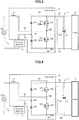
- Fig. 3 is a drawing showing paths of currents flowing through the circuit when the diode rectifying is performed in a case where the AC power source voltage has a positive polarity.
- a current flows in a direction indicated by broken line with an arrow. More specifically, the current flows from the AC power source VS, via the reactor L1, the parasitic diode D3, the smoothing capacitor C1, the shunt resister R1, and the diode D2 to the AC power source VS in this order.
- Fig. 4 is a drawing showing paths of currents flowing through the circuit when a diode rectification is performed in a case where the AC power source voltage has a negative polarity.
- the current flows in the direction indicated by the broken line with an arrow in a half cycle period in which the AC power source voltage Vs is negative. More specifically, the current flows from the AC power source VS, via the diode D1, the smoothing capacitor C1, the shunt resister R1, the parasitic diode D4, and the reactor L1, to the AC power source VS in this order.
- the controller 5 performs the synchronous rectification by switching control of the MOSFETs Q1, Q2 in accordance with the polarity of the AC power source voltage Vs to perform a higher efficiency operation than the diode rectification.
- a conversion efficiency of the converter 2 becomes the highest as compared with other modes because the number of times of switching is low in the rectifying operation. In the rectifying operation, a calculation load on the microcomputer for the control of the converter 2 is lowest as compared with other modes.
- Fig. 5 is a drawing showing paths of currents flowing through the circuit when a synchronous rectification is performed in a case where the AC power source voltage Vs has a positive polarity.
- Fig. 5 in a half period in which the AC power source voltage Vs is positive, the current flows in the direction indicated with the broken line with an arrow. More specifically, the current flows from the AC power source VS, via the reactor L1, the MOSFET Q1, the smoothing capacitor C1, the shunt resister R1, and the diode D2, to the AC power source VS in this order. In this state, the MOSFET Q2 is always tuned off and the MOSFET Q1 is always turned on. If it is assumed that the MOSFET Q1 is not turned on, as described diode rectification operation, the current flows through the parasitic diode D3 of the MOSFET Q1.
- timing of start of ON operation of the MOSFET Q1 is timing of zero cross when the polarity of the AC power source voltage Vs changes to positive from negative.
- Timing of turning off the MOSFET Q1 is timing when the polarity of the AC power source voltage Vs changes to negative from positive.
- Fig. 6 is a drawing showing paths of currents flowing through the circuit when the synchronous rectification is performed in a case where the AC power source voltage Vs has the negative polarity.
- a current flows in a direction indicated by broken line with an arrow. More specifically, the current flows from the AC power source VS, via the diode D1, the smoothing capacitor C1, the shunt resister R1, the MOSFET Q2, the reactor L1, and the AC power source VS in this order.
- the MOSFET Q1 is always turned off and the MOSFET Q2 is always turned on.
- timing of start of ON operation of the MOSFET Q2 is timing of the zero cross when the polarity of the AC power source voltage Vs changes from positive to negative.
- Timing of turning on of the MOSFET Q1 is timing when the polarity of the AC power source voltage Vs changes to negative from positive.
- Timing of turning off the MOSFET Q1 is timing when the polarity of the AC power source voltage Vs changes to negative from positive.
- the converter 2 is operated, which provides a high efficiency.
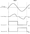
- Fig. 7 shows waveforms showing a relation among an AC voltage and AC current flowing through a motor, and pulse signals.
- a first graph in Fig. 7 shows a waveform of an instantaneous magnitude vs of the AC power source voltage Vs and a second graph indicates a waveform of the circuit current i s .
- a third graph in Fig. 7 shows a waveform of drive pulses for the MOSFET Q1 and a fourth graph of Fig. 7 shows a waveform of drive pulses for the MOSFET Q2.
- the instantaneous magnitude vs of the AC power source voltage Vs has a substantially sine waveform as shown in the first graph in Fig. 7 .
- the drive pulses for the MOSFET Q1 are, as shown in a third graph in Fig. 7 , have a H level when the polarity of the AC power source voltage Vs is positive and a L level when the polarity of the AC power source voltage Vs is negative .
- the drive pulses of the MOSFET Q2 are the inverse of the drivel pulses for the MOSFET Q1 and have the L level when the polarity of the AC power source voltage Vs is positive and has the H level when the polarity of the AC power source voltage Vs is negative.
- the circuit current flows when the AC power source voltage Vs reaches a predetermined amplitude, i.e., when the AC power source voltage Vs is greater than the DC voltage Vd.
- the high speed switching operation for boosting the DC voltage Vd and improving the power factor is described below.
- the power inputted from the AC power source VS is greater than that in the other modes.
- the high speed switching operation has a boosting power of boosting the DC voltage of the converter 2 and a harmonic component suppression efficient which are higher than those of the other modes.
- boosting the DC voltage Vd and improvement in the power factor are performed by shorting the circuit through the reactor L1 by switching control for the MOSFETs Q1 and Q2 at a certain switching frequency (hereinafter referred to as power factor improvement operation) to allow short circuit current to flow in the circuit (hereinafter referred to as power factor improvement current).
- power factor improvement operation switching control for the MOSFETs Q1 and Q2 at a certain switching frequency
- the power factor improvement is performed by approaching the circuit current i s to a sine wave to reduce harmonic component currents.
- Fig. 8 is a drawing showing paths of currents flowing through the circuit when the synchronous rectification is performed in a case where the AC power source voltage Vs has a positive polarity.
- a short circuit current i sp flows on a path from the AC power source VS, via the reactor L1, the MOSFET Q2, and the diode D2, to the AC power source VS in this order.
- energy is stored in the reactor L1 represented in Eq. (1).
- Fig. 9 is a drawing showing paths of currents flowing through the circuit when a power factor improvement is performed in a case where the AC power source voltage has a negative polarity.
- the current in the current path flows from the AC power source VS, via the diode D1, the MOSFET Q1, and the reactor L1, to the AC power source VS in this order.
- energy is stored in the reactor L1, and the energy boosts the DC voltage Vd.
- Fig. 10 shows waveforms of the power supply voltage, the circuit current, and the driving pulses for MOSFETs when the partial switching (two shuts) is performed.
- a first graph in Fig. 10 shows a waveform of the moment value vs of the AC power source voltage Vs and a second graph shows a waveform of the circuit current i s .
- a third graph in Fig. 10 shows a waveform of the driving pulses for the MOSFET Q1, and a fourth graph shows driving pulses for the MOSFET Q2.
- the instantaneous magnitude vs of the AC power source voltage Vs has a waveform having a substantially sine waveform shape.
- the driving pulses for the MOSFET Q1 becomes H level when the polarity of the AC power source voltage Vs is positive, and two L level pulses are generated at a predetermined timing.
- the drive pulse becomes L level and then two H level pulses are generated at a predetermined timing.
- the driving pulses for the MOSFET Q2 are the inverse of the driving pulses for the MOSFET Q1. This is because the power-factor improvement operation and the synchronous rectification operation are combined. For example, when the AC power source voltage Vs has a positive polarity, the MOSFET Q2 is turned on to perform the power-factor improvement operation. After that, a period where the MOSFET Q2 is turned on after turning off of the MOSFET Q1 is for the synchronous rectification operation. As described above, the high efficiency operation can be done with the power-factor improvement by combining the power-factor improvement operation and the synchronous operation.
- the circuit current rises when the AC power source voltage Vs has the positive polarity and the driving pulse for the MOSFET Q2 becomes H level and rises when the AC power source voltage Vs has the negative polarity and the driving pulse for the MOSFET Q1 becomes H level. This improves the power factor.
- the current path in the power-factor improvement operation is as shown in Fig. 8 .
- the power-factor improvement operation and the diode rectification operation. More specifically, when the polarity of the AC power source voltage Vs is positive, the current path in the power-factor improvement operation is as shown in Fig. 8 . After the MOSFET Q2 is turned off, the parasitic diode D3 turns on, so that the mode changes into the diode rectification operation. The current path in this state is as shown in Fig. 3 .
- Fig. 11 shows waveforms of a power supply voltage, a circuit current, and driving pulses for the MOSFET when a high-speed switching is performed.
- a first graph in Fig. 11 shows a waveform of the instantaneous magnitude vs of the AC power source voltage Vs, and a second graph in Fig. 11 shows a waveform of the circuit current i s .
- a third graph in Fig. 11 shows driving pulse waveforms for the MOSFET Q1 and a fourth graph in Fig. 11 shows driving pulse waveform for the MOSFET Q2.
- the instantaneous magnitude vs of the AC power source voltage Vs have a substantial sine waveform shape.
- the high speed switching operation for example, when the power source voltage is positive in the polarity, the short circuit current i sp is allowed to flow by turning on the MOSFET Q2 and turning off the MOSFET Q1. Next, the MOSFET Q2 is turned off and the MOSFET Q1 is turned on. As described above, switching is made between turning on and off of a MOSFET Q1 and MOSFET Q2 in accordance with existence of the power-factor improvement operation. This is made for the synchronous rectification is performed. For example, when interruption, etc. is used in the microcomputer, the calculation load on the microcomputer for the control for the converter 2 becomes larger than that in the other modes.
- the circuit current i s can be shaped in a sine wave by performing the high speed switching operation to have a high power factor.
- the switching loss increases.
- harmonic component currents it becomes difficult to satisfy a limit value of harmonic component currents because as a circuit input increases, harmonic component currents largely increases, so that it is required to secure a high power factor as increase in the input current. Contrary to this, when the input is small, the harmonic component current is small. Accordingly, there may be a case that it is not necessary to secure a power factor more than necessary. In other words, it is sufficient to reduce the harmonic component current by keeping an appropriate power factor while an efficiency is considered in accordance with the load condition.
- the power inputted from the AC power source VS during the partial switching operation is greater than power in the rectification operation and smaller than the power during the high speed switching operation.
- the controller 5 uses a DTC (Data Transfer Control) function provided to the microcomputer.
- the DTC function is a hardware function of outputting pulses having a predetermined pattern at a preset timing. According to the DTC function, it is possible to output pulses having a predetermined pattern at accurate timing without influence of delay in software calculation in the microcomputer.
- the microcomputer in the embodiment includes two channels of the DTC functions.
- the partial switching operation is not performing the power-factor improvement operation at a predetermined frequency like the high speed switching, but an operation mode, in which the DC voltage Vd is boosted and the power factor is improved by performing a plurality of times of the power-factor improvement operation at a predetermined phase in a half cycle of the AC power source voltage Vs. This can reduce the switching loss by decrease in the number of times of switching of the MOSFET Q1 and the MOSFET Q2 more than the case of the high speed switching operation.
- the partial switching operation is described below.
- Fig. 12 is a drawing explaining outline of the partial switching.
- a first graph in Fig. 12 shows the instantaneous magnitude vs of the AC power source voltage Vs, and a second graph shows the circuit current i s .
- a third graph in Fig. 12 shows driving pulses for the MOSFET Q2, and a fourth graph shows the driving pluses for the MOSFET Q1.
- the instantaneous magnitude vs of the AC power source voltage Vs has a substantially sine wave shape.
- a dashed line in the second graph in Fig. 12 shows an ideal circuit current i s in a substantially sine wave shape. The power factor is most improved in this state.
- the converter 2 can perform the diode rectification control, the synchronous rectification control, and the partial switching control, and the high speed switching control. For example, depending on the type of the used device, a required performance may be changed in accordance with the load condition at a region in which the high efficiency is prioritized, a region in which the boosting and the power-factor improvement are prioritized, etc. Then, it is possible to perform high efficient control and reduction in the harmonic component current compatibly by switching among the four modes on the basis of predetermined threshold information.
- Fig. 13 is a drawing of a current waveform before switching from the partial switching to the high speed switching.
- Fig. 13 schematically shows the instantaneous magnitude vs of the AC power source voltage Vs and the input current Is.
- Fig. 14 is a drawing showing a current waveform after the switching from the partial switching to the high speed switching.
- Fig. 14 schematically shows the instantaneous magnitude vs of the AC power source voltage Vs when the control is changed into the high speed switching control.
- the peak of the circuit current i s at this instance is smaller than a peak of the current i s shown in Fig. 13 .
- the control is switched with adjustment of the ON interval can suppress a variation of the DC voltage Vd. This is because the current becomes small because the high speed switching has a better power factor than the partial switching.
- the DC voltage Vd is excessively boosted. This can suppress the variation in the DC voltage Vd.
- switching between respect controls can be performed stable at timing of zero cross of the power source voltage.
- Fig. 15 is a drawing showing a circuit configuration of the inverter 3a.
- Fig. 15 shows a circuit configuration of the inverter 3a included in the power converter 1 having a PWM (Pulse Width Modulation) control method according to the embodiment of the present invention.
- the power converter 1 drives the motor 4a, which is a permanent magnet synchronous motor, by vector control with the inverter 3a including three-phase inverter for driving by PWM control. In this case, control is performed by providing phase pulse stop intervals (open phase interval) in the pulse signal of the inverter 3a.
- the inverter 3b is configured similarly to the inverter 3a, and its description is omitted.
- the power converter 1 includes the inverter 3a, the phase current detector 15a, and the load controller 19a.
- the inverter 3a can perform intermittent energization in which switching a motor current around zero cross of the motor current while the DC power is converted into three-phase AC power.
- the phase current detector 15a detects a motor current flowing in the motor 4a, which is an AC motor connected to the inverter 3a.
- the load controller 19a performs the vector control using the pulse signal for PWM control on the basis of the phase current information (current) ⁇ detected by the phase current detector 15a.
- the inverter 3a is configured including a gate driver 32 and a power converting circuit 31.
- the gate driver 32 generates gate signals supplied to each of IGBTs (Insulated Gate Bipolar Transistor) in the power converting circuit 31 on the basis of a pulse signal ⁇ supplied from a pulse controller 193.
- IGBTs Insulated Gate Bipolar Transistor
- the power converting circuit 31 is configured including switching elements Q3 to Q8, each including IGBT and a diode are connected in parallel in opposite directions.
- the power converting circuit 31 is configured including switching legs having a three-phase structure of U-, V-, and W-phases, converts a DC power into an AC power using pulse signals ⁇ outputted by the pulse controller 193.
- the U-phase switching leg is configured including switching elements Q3, Q4 which are connected in series between positive and negative terminals thereof.
- a collector of the switching element Q3 is connected to the positive terminal, and an emitter of the switching element Q3 is connected to a collector of a switching element Q4.
- An emitter of the switching element Q4 is connected to the negative terminal.
- a junction node of the emitter of the switching element Q3 and the collector of the switching element Q4 is connected to a U-phase coil of the motor 4a. Let a voltage of the junction node of the emitter of the switching element Q3 and the collector of the switching element Q4 be a voltage Vu, and let a current flowing in the U-phase coil of the motor 4a be U-phase AC current Iu.
- a gate of the switching element Q3 is supplied with a pulse signal GPU+ outputted by the gate driver 32.
- a gate of the switching element Q4 is supplied with a pulse signal GPU- outputted by the gate driver 32.
- the U-phase switching leg is configured including switching elements Q5, Q6 which are connected in series between positive and negative terminals thereof.
- a collector of the switching element Q5 is connected to the positive terminal, and an emitter of the switching element Q5 is connected to a collector of a switching element Q6.
- An emitter of the switching element Q6 is connected to the negative terminal.
- a junction node of the emitter of the switching element Q5 and the collector of the switching element Q6 is connected to a V-phase coil of the motor 4a.
- Gates of the switching elements Q5, Q6 are supplied with pulse signals outputted by the gate driver 32, respectively.
- the W-phase switching leg is configured including switching elements Q7, Q8 which are connected in series between positive and negative terminals thereof.
- a collector of the switching element Q7 is connected to the positive terminal, and an emitter of the switching element Q7 is connected to a collector of a switching element Q8.
- An emitter of the switching element Q8 is connected to the negative terminal.
- a junction node of the emitter of the switching element Q7 and the collector of the switching element Q8 is connected to a W-phase coil of the motor 4a.
- Gates of the switching elements Q7, Q8 are supplied with pulse signals outputted by the gate driver 32, respectively.
- the load controller 19a is configured including the pulse controller 193, a vector controller 191, and a pulse stop controller 192.
- the vector controller 191 performs vector control using the phase current information ⁇ detected by the phase current detector 15a to calculate an application voltage command V*.
- the pulse controller 193 supplies the pulse signal ⁇ controlled on the basis of the application voltage command (command voltage) V* to the gate driver 32 to cause the gate driver 32 to perform the PWM control.
- the pulse stop controller 192 generates a phase pulse stop control signal (pulse stop control signal) ⁇ on the basis of phase information (current phase) ⁇ of the current calculated by the vector control.
- the phase pulse stop control signal (pulse stop control signal) ⁇ is for stopping the pulse signal ⁇ in the phase pulse stop interval (open phase interval) ⁇ around current zero-cross and supplied to the pulse controller 193.
- the controller 5 uses the DTC function of the microcomputer to output the phase pulse stop control signal (pulse stop control signal) ⁇ at predetermined timing.
- the vector controller 191 is provided using a general vector control and the control method is not specified.
- the general vector control is, for example, an inverter is driven by detecting an inverter output current which is three-phase/two-phase-converted (dq-conversion; direct-quadrature conversion) and fed back to the control system and two-phase-three-phase-converted again as disclosed in a non-patent Document 1, " A simplified vector control is proposed as a driving method of permanent magnet synchronous motor (PMSM) for electrical household appliances", by Sakamoto, etc. paper of the Institute of Electrical Engineers of Japan, D, Vol. 124, No.
- PMSM permanent magnet synchronous motor
- Fig. 16 shows waveforms showing a relation among an AC voltage and AC current flowing through a motor, and pulse signals, in which the axes of abscissa represents a voltage phase, the axes of ordinate represent respective level of the voltage, the current, and respective levels of the pulse signals.
- the load controller 19a (see Fig.15 ) generates a PWM pulse signal by comparing a PWM carrier signal and the application voltage command V* as shown in the first graph in Fig. 16 .
- a command value of the application voltage command V* is obtained by performing a calculation by the vector controller 191 on the basis of the phase current information ⁇ detected by the phase current detector 15a.
- Obtaining the phase current information ⁇ by the phase current detector 15a may be done by directly detecting AC output current by a CT (Current Transformer) as disclosed in Fig .1 in JP2004-48886 A , and a method of reproducing the phase current on the basis of the current information detected by a shunt resistor as disclosed in Fig. 12 in JP2004-48886 A .
- the first graph in Fig. 15 shows the PWM carrier signal and the application voltage command V* and representatively, a U-phase application voltage command Vu* is shown.
- ⁇ v represents a voltage phase with reference to the U phase.
- the pulse controller 193 In the PWM control method, the pulse controller 193 generates pulse signals GPU+, GPU- shown in the third graph in Fig. 16 on the basis of the U-phase application voltage command Vu* and a triangle wave carrier signal (PWM carrier signal), and supplies these pulse signals GPU+, GPU- to the DC voltage waveform 32 to drive the carrier wave 31. Further, a pulse signal GPU+ is applied to the gate of the switching element Q3 on an upper side of the U-phase. The pulse signal GPU- is applied to the switching element Q4 disposed on a lower side of the U-phase. In other words, the pulse signals GPU+, GPU- are inverse signals regarding positive and negative (1, 0).
- the carrier wave 31 performs the PWM control using the pulse signals GPU+, GPU-, so that a U-phase AC current Iu as shown in the second graph in Fig. 16 flows through the motor 4a.
- ⁇ represents a phase difference between the voltage and current.
- the vector controller 191 controls a voltage amplitude and the phase difference ⁇ by performing the vector control on the basis of the phase current information ⁇ including the U-phase AC current Iu.
- the switching operation in one cycle of the voltage and current, the switching operation is always done to provide 180-degree energization, so that the number of times of switching is larger than those of the 120-degree energization method and 150-degree energization method. Accordingly, in the 180-degree energization, the switching loss caused by this increases.
- Fig. 17 shows waveforms showing a relation among an AC voltage and AC current, flowing through the motor, and phase pulse stop control signals.
- the axes of abscissas represent a voltage phase.
- Axes of ordinate represents, voltage, current, and levels of the pulse signal and an open phase control signal (phase pulse stop control signal), respectively.
- Fig. 17 shows waveforms of the intermittent energization operation as compared with the waveforms in the general operation shown in Fig. 16 .
- the pulse stop controller 192 supplies the phase pulse stop control signal (open phase control) ⁇ to stop switching the pulse signal GPU+, GPU- in the phase pulse stop intervals (open phase control signal at a phase ⁇ and a phase ⁇ + ⁇ , referring to the zero cross point ⁇ of the current phase controlled by the vector control as a reference, as shown in Eq. (2) below.
- the pulse stop control signal ⁇ has a value of "0", when switching in both the pulse signals GPU+, GPU- are stopped, and a value of "1" when the switching stop is not made, but PWM control switching are made.
- ⁇ ⁇ 0 When ⁇ ⁇ ⁇ 2 ⁇ ⁇ ⁇ ⁇ + ⁇ 2 0 When ⁇ + ⁇ ⁇ ⁇ 2 ⁇ ⁇ ⁇ ⁇ + ⁇ + ⁇ 2 1
- ⁇ be a phase difference between the voltage and the current
- ⁇ be pulse stop interval (open phase interval)
- the switching by the pulse signal GPU+ and GPU- is stopped.
- the switching by the pulse signals GPU+ and GPU- is stopped.
- the output state of the pulse controller 193 is such that both the pulse signals GPU+ andGPU- are turned off at the phase pulse stop interval ⁇ . Then, the pulse controller 193 outputs a signal train of pulse signals in which the pulse is not outputted in the phase pulse stopping interval ⁇ as shown in the third graph of the Fig. 17 .
- phase pulse stopping intervals (open phase intervals) ⁇ are set twice in one-cycle of the voltage and the current. Further, in the configuration according to the present embodiment, it is possible to provide a similar phase pulse stopping interval ⁇ in a two-phase modulation type PWM control method, or a third-harmonic component addition type PWM control method in addition to the sine wave PWM control method.
- the pulse signals GPU+, GPU- in which the intervals of stopping the switching operation are provided by the pulse stop controller 192 have waveforms in which the switching is not made with reference to the applied voltage phase and an induced voltage phase of the inverter circuit 4. More specifically, the switching stopping interval and the switching operation interval are provided with reference to the zero-cross point of the current phase.
- the pulse signals are pulse signals referring to the voltage phase of the induced voltage
- the pulse signal train having ON/OFF duties before and after the zero cross point are symmetrical as shown in the third graph of Fig. 16 .
- the phase pulse stopping interval ⁇ is provided with reference to the current phase (i.e., it is not the pulse signal refereeing to the voltage phase)
- the ON/OFF duty are not symmetrical before and after the voltage zero cross point.
- the ON/OFF duty of the pulse signal train before and after the current zero cross point are asymmetrical.
- phase pulse stop interval ⁇ is provided in the interval including zero-cross of the current
- pulse trains A and B before and after the phase pulse stop interval ⁇ as a center have asymmetric shapes. Accordingly, when the phase pulse stop interval ⁇ is provided in the interval including zero-cross points of the current, it is easy to determine whether the intermittent energization operation according to the present embodiment is applied or not by observing to determine whether the pulse signals before and after the phase pulse stop interval ⁇ are asymmetry or not.
- Fig. 18 shows waveforms showing a relation among a U-phase voltage, a U-phase current, and pulse signals when an actual device is driven including the inverter 3a according to the present embodiment, where the axes of abscissa represents the voltage phase, and the axes of ordinate represents the voltage, the current and levels of pulse signals. More specifically, Fig. 18 shows the voltage, the current, and the pulse signals when the phase pulse stop interval is set in the two-phase modulation type PWM control method by a technology of providing the phase pulse stop interval around the zero-cross points of the current according to the first embodiment.
- a first graph of Fig. 18 shows a U-phase terminal voltage Vun of the power converting circuit 31, and a second graph of Fig. 18 shows the U-phase AC current Iu flowing in a AC motor 3.
- a third graph of Fig. 18 shows the pulse signal GPU+, and a fourth graph of Fig. 18 shows a GPU- signal.
- Fig. 19 is a characteristic drawing showing a relation among a power conversion circuit loss for a phase pulse stop period (open phase period) ⁇ by the intermittent energization with the inverter 3a, and a total loss derived by adding them.
- the characteristic drawing represents the phase pulse stop interval (open phase interval) ⁇ on the axis of abscissa and the loss on the axis of ordinate. More specifically, Fig. 19 shows the phase pulse stop interval ⁇ set by the pulse stop controller 192 and the loss in the inverter 3a, and a loss in the AC motor (the motor 4a), and a total loss characteristic derived by summing the two losses.
- the loss (power converting circuit loss) of the inverter 3a decreases as decrease in the number of times of switching as increases in the phase pulse stop interval ⁇ . Further the loss (motor loss) of the motor 4a (AC motor) largely increases because harmonic components of the current increases by provision of the phase pulse stop interval ⁇ . Further, increase in the phase pulse stop interval ⁇ increases the harmonic components of the current remarkably, so that the loss (motor loss) of the motor 4a (AC motor) caused by this reason also increases remarkably. Accordingly, as shown in Fig.
- phase pulse stop interval ⁇ opt in which the total loss becomes smallest, the total loss being derived by summing these losses (power converting circuit loss and the motor loss). Setting the phase pulse stop interval ⁇ to the phase pulse stop interval ⁇ opt can decrease the entire loss of the power converter 1.
- using the pulse stop controller 192 can reduce the number of times of switching of the pulse signal for PWM control using the pulse stop controller 192.
- the pulse stop controller 192 operated under control of the microcomputer is configured as software, it is possible to reach a high efficiency of the power converter 1 without addition of a new hardware without modification in the configuration of the inverter 3a. Further, because the switching operation around the zero-cross of the current of the motor 4a is stopped, it is possible to suppress increase in the torque pulsation for the 150-degree energization method.
- Fig. 20 is a front view of an indoor device 100, an outdoor device 200, and a remote controller of the air conditioning device A according to the embodiment of the present invention.
- an air conditioner A is one type of refrigeration air conditioners, so-called a room air conditioner.
- the air conditioner A includes an indoor device 100, an outdoor device 200, a remote controller Re, the converter 2, the inverters 3a, 3b shown in Fig. 1 .
- the indoor device 100 and the outdoor device 200 are connected with refrigerant tubes 300 which perform air-conditioning a room in which the indoor device 100 is installed through the known refrigeration cycle. Further, the indoor device 100 and the outdoor device 200 transmit and receive information each other through a communication cable (not shown). Further, the outdoor device 200 is connected with wiring (not shown) to be supplied with an AC voltage through the indoor device 100.
- the power converter 1 (see Fig. 1 ) is installed in the outdoor device 200 and converts the AC power supplied from the side of the indoor device 100 into the DC power.
- the remote controller Re is operated by a user and transmits an infrared signal to a remote controller signal transmitting and receiving section Q of the indoor device 100.
- Contents of the infra-red signal is a command for requesting operation, change of setting temperature, a timer, change of the operation mode, a request for stop, etc.
- the air conditioner A performs airconditioning operations in a cooling mode, a heating mode, a dehumidifying mode, etc on the basis of the command in the infra-red signal.
- the indoor device 100 transmits room temperature information, humidity information, an electrical charge to the remote controller Re from the remote controller signal transmitting and receiving section Q.
- the power converter 1 performs boosting the DC voltage Vd with reduction in the harmonic component current by increased efficiency operation and improvement in the power factor and conversion into the AC power to drive the motors 4a, 4b.
- the converter 2 includes as described above four operation modes, i.e., the diode rectification operation, the synchronous rectification operation, the high speed switching operation, and the partial switching operation.
- the loads H are the inverters 3a, 3b and the motors 4a, 4b.
- the load is small and high efficiency operation is required, it is preferable to operate the converter 2 in the synchronous rectification mode.
- the converter 2 When the load is large and it is required to secure boosting and a high power factor, it is preferable to control the converter 2 to perform high speed switching. Further, when the boosting and security of the power factor are required though the load is not so large like the rated operation of the air conditioner A, it is preferable to perform the partial switching operation. Further, when the partial switching and the high speed switching are performed, either of the diode rectification operation and the synchronous rectification operation is further combined.
- Fig. 21 shows states of switching the operation modes of the converter 2 and the inverters 3a, 3b.
- the converter 2 for converting the power source voltage into the DC voltage performs rectification and boosting operation in three operation modes as follows:
- the rectification operation is an operation mode for performing only rectification operation without performing the shorting operation in which the power supplied from the AC power source VS is lower than that in the other modes. Because the number of times of switching is small in the rectification operation, the conversion efficiency of the converter 2 is largest as compared with other modes. In the rectification operation, an operation load on the microcomputer of control by the converter 2 is smallest as compared with other modes.
- the partial switching operation is an operation mode of performing the shorting operation of a plurality times (one to ten times) per one cycle of the power source voltage and the rectification operation alternately.
- the power inputted from the AC power source VS in this mode is higher than that in the rectification operation and lower than that in the high speed switching operation.
- the controller 5 uses the DTC function of the microcomputer to output pulses at predetermined timing.
- the high speed switching operation is an operation mode performing the shorting operation and the rectification operation alternately in the PWM cycle (higher than several KHz).
- the power inputted from the AC power source VS is higher than other modes.
- the boosting performance increasing the DC voltage of the converter 2 and a suppressing effect of the harmonic components are higher than those in other modes.
- the operation load on the microcomputer of the control of the converter 2 is largest as compared with other modes.
- the converter 2 when the output is low, i.e., in an intermediate condition on the basis of APF (Annual Performance Factor) standard, the converter 2 performs the rectification operation.
- the output is at a middle range, i.e., at the rated condition on the basis of the APF standard, the converter 2 performs the partial switching operation.
- the converter 2 When the output is at a high range, i.e., in a low heating power condition on the basis of the APF standard, the converter 2 performs the high speed switching operation. Accordingly the converter 2 boosts the DC voltage and can drive a permanent magnet motor at a high efficiency.
- the controller 5 controls the converter 2 to perform the boosting operation and the inverters 3a, 3b to perform the intermittent energization operation linkingly. Because the intermittent energization operation has a high effect in increasing efficiency, when the intermittent energization is performed when the output level is low, this provides a high effect in improved efficiency. However, to output the pulse at predetermined timing, the DTC function of the microcomputer is used. Accordingly, it is necessary to determine whether the inverters 3a, 3b are operated in the intermittent energization operation or not and whether the converter 2 is operated in the partial switching operation due to a limit of the number of channels of the DTC function of the microcomputer.
- the operation mode of the converter 2 and presences of the intermittent energization operation of the inverter A (inverter 3a) and the inverter B (inverter 3b) are combined as shown in Fig. 21 .
- the controller 5 controls the inverters 3a, 3b to perform the intermittent energization and the converter 2 to perform the rectification operation using two channels of DTC function.
- the controller 5 controls either of the inverters 3a, 3b to perform the intermittent energization using one channel of the DTC function and the converter 2 to perform the partial switching operation using one channel of the DTC unction.
- the controller 5 controls the inverters 3a, 3b in general operation and the converter 2 to perform the high speed switching operation.
- the controller 5 does not use the DTC function.
- the controller 5 can drive the permanent magnet synchronous motor in accordance with the input by performing the boosting operation of the converter 2 and the intermittent energization of the inverters 3a, 3b linkingly, so that the permanent magnet motor can be driven at a high efficiency in accordance with the input.
- the present invention is not limited to the above-described embodiment and has various modifications.
- the above-described embodiments have been described in detail to have easy understanding, but not limited to the power converter and refrigeration air conditioner including all elements described above. It is possible to replace a part of the configuration of an embodiment with a part of configuration of another embodiment and also add a part of the configuration of one embodiment to configuration of another embodiment. Further, it is possible to add to, omit, or replace with configuration of another configuration.
- control line and data line are shown in figures for only necessary part, and it is not always to show all control lines and data lines in the product. Actually, almost all elements are connected with each other.
Landscapes
- Engineering & Computer Science (AREA)
- Power Engineering (AREA)
- Rectifiers (AREA)
- Inverter Devices (AREA)
- Ac-Ac Conversion (AREA)
- Control Of Ac Motors In General (AREA)
Abstract
Description
- The present invention relates to a power converter and a refrigeration air conditioner.
- A converter circuit for converting a single-phase AC voltage into a DC voltage repeats, in response to an output, an operation of storing energy in a reactor by short-circuiting through the reactor and discharging the energy in the reactor during rectifying operation. According to this, the converter circuit boosts the DC voltage to have high efficiency and high output of a permanent magnetic synchronous motor.
- Further, an inverter circuit converts the DC voltage into three-phase AC power to drive the permanent synchronous motor and performs an intermittently energization control in which switching around a current zero cross is turned off. According to this, the power converting circuit and the permanent magnet synchronous motor are aimed to have high efficiencies. In other words, the boosting operation of the converter circuit and the intermittent energization operation of the inverter are performed in accordance with the input and the output to have high efficiency of the power converter.
- Further, a cost reduction in the power converter can be provided by driving a plurality of motors with a single microcomputer. However, when a single microcomputer performs operations, the microcomputer may not able to control the converter circuit and the inverter circuit.
- PATENT DOCUMENT 1:
JP 5718474 -
PATENT DOCUMENT 1 disclosed only the intermittent energization operation on an inverter circuit side. In this configuration, the intermittent energization operation may be performed independently from the operation on the converter circuit side. In other words, when the operation is performed by a single microprocessor, there is a possibility in that the motor cannot be controlled due to increase in the operation load. Accordingly, it is efficient that the boosting operation and the intermittent energization control are performed linkingly in accordance with output conditions to reduce the operation load. - An aspect of the present invention provides a power converter and a refrigeration air conditioner using the same to optimally perform the boosting operation of the power converter and the intermittent energization operation of the inverter in accordance with the input and the output.
- To solve the problem, the power converter according to the present invention includes a converter capable of boosting a DC voltage by a switching operation alternately performing short-circuiting and rectification through a reactor in a power source, an inverter capable of an intermittent energization to make switching around zero cross of a motor current OFF while a DC voltage outputted by the converter is converted into three-phase AC power, and a controller for performing the boosting operation of the converter and the intermittent energization operation of the inverter interlockingly.
- Other means are described in the descriptions of the embodiments below.
- According to the configuration of the present invention, a high efficiency power converter can be driven in which the boosting operation of the converter and the intermittent energization operation of the inverter are optimally performed in accordance with the input and the output.
- According to the present invention, a power converter and a refrigeration air conditioner using the power converter to optimally perform the boosting operation of the converter and the intermittent energization operation of the inverter in accordance with the input and the output.
-
-
Fig. 1 is a general block diagram showing a power converter according to embodiments of the present invention.Fig. 2 is a general block diagram showing a converter and a controller. -
Fig. 3 is a drawing showing paths of currents flowing through the circuit when a diode rectification is performed in a case where the AC power source voltage has a positive polarity. -
Fig. 4 is a drawing showing paths of currents flowing through the circuit when a diode rectification is performed in a case where the AC power source voltage has a negative polarity. -
Fig. 5 is a drawing showing paths of currents flowing through the circuit when a synchronous rectification is performed in a case where the AC power source voltage has a positive polarity. -
Fig. 6 is a drawing showing paths of currents flowing through the circuit when the synchronous rectification is performed in a case where the AC power source voltage has the negative polarity. -
Fig. 7 shows waveforms of a power supply voltage, a circuit current, and driving pulses in the synchronous rectification. -
Fig. 8 is a drawing showing paths of currents flowing through the circuit when a synchronous rectification is performed in a case where the AC power source voltage has a positive polarity. -
Fig. 9 is a drawing showing paths of currents flowing through the circuit when a power-factor improvement is performed in a case where the AC power source voltage has a negative polarity. -
Fig. 10 shows waveforms of a power supply voltage, a circuit current, and driving pulses for a MOSFET when a partial switching (two shuts) is performed. -
Fig. 11 shows waveforms of a power supply voltage, a circuit current, and driving pulses for the MOSFET when a high-speed switching is performed. -
Fig. 12 is a drawing explaining outline of the partial switching. -
Fig. 13 is a drawing of a current waveform before switching from the partial switching to the high speed switching. -
Fig. 14 is a drawing showing a current waveform after the switching from the partial switching to the high speed switching. -
Fig. 15 is a drawing showing a circuit configuration of an inverter. -
Fig. 16 shows waveforms showing a relation among an AC voltage and AC current flowing through a motor, and pulse signals while the inverter operates. -
Fig. 17 shows waveforms showing a relation among an AC voltage and AC current flowing through the motor, and phase pulse stop control signals. -
Fig. 18 shows waveforms a relation among a U-phase voltage, a U-phase current, and pulse signals when an actual device is driven. -
Fig. 19 is a characteristic drawing showing a relation among a power conversion circuit loss for a phase pulse stop interval (open phase interval) δ and a motor loss by an inverter intermittent energization operation and a total loss derived by adding them. -
Fig. 20 is a front view of an indoor device, an outdoor device, and a remote controller of the air conditioning device according to the embodiment of the present invention.Fig. 21 is an outline drawing illustrating states of switching from the operation mode of a converter and an operation mode of the inverter. - Embodiments according to the present invention are described below, referring to drawings.
-
Fig. 1 is a general block diagram showing apower converter 1 according to the present embodiment. - The
power converter 1 includes aconverter 2 connected to a AC power source VS, aninverter 3a, and amotor 4a, aninverter 3b, and amotor 4b, and acontroller 5 for integrally controlling them. Thepower converter 1 further includes acurrent detector 11, a smoothing capacitor C1, phasecurrent detectors power converter 1 is installed in the air conditioning device. On the drawing, theinverter 3a is referred to as "an inverter A", and theinverter 3b is referred to as "an inverter B". - The
converter 2 converts a power supply voltage into a DC voltage and can boost the DC voltage outputted by the switching operation performing short circuiting through a coil in the power supply and rectification alternately. Theinverter 3a is provided to rotationally drive themotor 4a with conversion of the DC voltage into an AC voltage. Themotor 4a is a fan motor for rotating a fan of the air conditioning device. Theinverter 3b converts the DC voltage into AC voltages to drive themotor 4b. Themotor 4b is a motor for a compressor to drive the compressor of the air conditioning device. Further, theinverter 3a and theinverter 3b have similar circuit configurations and drive themotors 4a - The
controller 5 controls theconverter 2 on the basis of a circuit current is detected by thecurrent detector 11, and a DC voltage Vd outputted by theconverter 2. Thecontroller 5 further controls theinverters current detectors controller 5 can control theconverter 2 to perform a boosting operation and theinverters - Referring to
Figs. 2 to 14 , configurations and operations of theconverter 2 and thecontroller 5 are described below. Further, referring toFigs. 15 to 19 , configurations and operations of theinverter 3a and thecontroller 5 are described below. -
Fig. 2 is a general block diagram showing theconverter 2 and thecontroller 5, etc. - As shown in
Fig. 2 , theconverter 2 converts an AC power source Vs supplied from the AC power source VS into the DC voltage Vd to supply the DC voltage Vd to a load H (inverters, motors, etc). Theconverter 2 is connected at an input side thereof to the AC power source VS and an output side thereof is connected to the load H. - The
converter 2 includes a reactor L1, the smoothing capacitor C1, diodes D1, D2, D3, D4, MOSFETs Q1, Q2, which are switching elements, and a shunt resister R1. The diodes D1, D2, D3, D4 and the MOSFETs Q1, Q2 form abridge rectifying circuit 10. - The MOSFETs Q1, Q2 are switching elements, and the diode D3 is a parasitic diode of the MOSFET Q1. The diode D4 is a parasitic diode of the MOSFET Q2. Further, saturation voltages of the MOSFET Q1 and the MOSFET Q2 are lower than forward voltage drops of the diode D3 and the parasitic diode D4.
- The diodes D1, D2 and the MOSFETs Q1, Q2 are connected in a bridge. An anode of the diode D1 is connected to a cathode of the diode D2, and a junction point N1 is connected to one terminal of the AC power source VS through a wiring hb.
- A source of the MOSFET Q1 is connected to a drain of the MOSFET Q2. The source of the MOSFET Q1 is connected to another terminal of the AC power source VS through a junction N2, a wiring ha, and the reactor L1.
- An anode of the diode D2 is connected to a source of the MOSFET Q2.
- A drain of the MOSFET Q1 is connected to a cathode of the diode D1.
- Further, the cathode of the diode D1 and the drain of the MOSFET Q1 are connected to a positive terminal of the smoothing capacitor C1 and one terminal of the load H through a wiring hc. Further, the diode D2 and the source of the MOSFET Q2 are connected to a negative terminal of the smoothing capacitor C1 and another terminal of the load H through the shunt resister R1 and the wiring hd.
- The reactor L1 is disposed in the wiring ha, i.e., between the AC power source VS and the
bridge rectifying circuit 10. The reactor L1 stores an electric power supplied from the AC power source VS as energy and discharges the energy, which provides boosting. - The smoothing capacitor C1 smoothes a voltage generated by rectifying through the diode D1 and the MOSFET Q1 into the DC voltage Vd. The smoothing capacitor C1 is connected to an output side of the
bridge rectifying circuit 10. i.e., a positive side is connected to the wiring hc, and a negative side is connected to a wiring hd. - The MOSFETs Q1, Q2, which are the switching elements, are controlled between ON and OFF in accordance with a command from a
converter controller 18 described later. Use of the MOSFETs Q1, Q2 as switching elements provides a high speed switching. Further, flowing a current through the MOSFET having a small voltage drop allows so-called synchronizing rectifying control, which reduces a circuit conduction loss. - In addition, superjunction MOSFETs, having a low ON resistance, are used as the MOSFETs Q1, Q2, which can further reduce the conduction loss. Incidentally, the parasitic diode of the MOSFET generates a reverse recovery current when a reverse voltage is applied by short-circuit operation. Particularly, the parasitic diode of the superjunction MOSFET has a reverse recovery current which is larger than that of parasitic diodes of general MOSFETs, which is a problem in that the switching loss is large. Accordingly, MOSFETs having a short reverse recovery time (trr: Reverse Recovery Time) are used as the MOSFETs Q1, Q2, which can reduce the switching loss.
- As the diodes D1, D2, it is preferable that diodes having small forward voltage drop are selected because the diodes D1, D2 do not generate the reverse recovery current even in active operation thereof. For example, it is possible to reduce a circuit conduction loss by using a general rectifying diode, or a Schottky barrier diode having a high AC voltage resistance.
- The shunt resister R1 has a function of detecting a momentary current flowing in the circuit.
- The
converter 2 is controlled by thecontroller 5. Thecontroller 5 includes again controller 12, anAC voltage detector 13, a zero-cross determining section 14, a boostingratio controller 16, aDC voltage detector 17, theconverter controller 18, andload controllers 19a, 19b. Thecontroller 5 receives sensor information from thecurrent detector 11, and the phasecurrent detectors - The
current detector 11 has a function of detecting an average current flowing in the circuit. - The
gain controller 12 has a function of controlling a current control gain Kp determined from a circuit current root-mean-square value Is and a DC voltage boosting ratio a. In this operation, controlling Kp × Is to a predetermined value provides boosting from the AC power source voltage Vs to a DC voltage which is a-times the DC voltage Vd. - The
AC voltage detector 13 is a detector for detecting the AC power source voltage Vs applied from the AC power source VS and connected to the wirings ha, hb. TheAC voltage detector 13 supplies the detection value to the zero-cross determining section 14. - The zero-
cross determining section 14 has a function of determining whether a polarity of the value of the AC power source voltage Vs detected by theAC voltage detector 13 changes, i.e., whether the AC power source voltage Vs reaches a zero-cross point. The zero-cross determining section 14 is a polarity detector detecting the polarity of the AC power source voltage Vs. For example, the zero-cross determining section 14 supplies, to theconverter controller 18, a signal of '1' in a period in which the AC power source voltage Vs is positive and a signal of '0' in a period in which the AC power source voltage Vs is negative. - The phase
current detectors inverters motors motors current detectors inverters DC voltage detector 17 and the applied voltage of themotors current detectors ratio controller 16 and theload controllers 19a, 19b. - The boosting
ratio controller 16 selects one of boosting ratios a of the DC voltages Vd from the detection values of the phasecurrent detectors converter controller 18. Theconverter controller 18 performs switching control by supplying driving pulses to the MOSFETs Q1, Q2 to perform switching control to boost the DC voltage Vd to target voltages. - The
DC voltage detector 17 is a sensor for detecting the DC voltage Vd applied to the smoothing capacitor C1, and a positive side thereof is connected to the wiring hc and the negative side thereof is connected to the wiring hd. TheDC voltage detector 17 supplies the detected value to theconverter controller 18. The detection value of theDC voltage detector 17 is used to determine whether the voltage value applied to the load H reaches a predetermined target value or not. - The
controller 5 including theconverter controller 18 is, for example, a microcomputer (not shown). The microcomputer reads out a program stored in ROM (Read Only Memory) and load the program to be stored on RAM (Random Access Memory), and a CPU (Central Processing Unit) performs various processes. Theconverter controller 18 controls ON/OFF of the MOSFETs Q1, Q2 on the basis of the information inputted from thecurrent detector 11 or the shunt resister R1, thegain controller 12, the zero-cross determining section 14, the boostingratio controller 16, and theDC voltage detector 17. The process executed by theconverter controller 18 will be described later. - The
load controllers 19a, 19b are controllers for respectively controlling theinverters Fig. 1 ) included in the load H. Theload controller 19a and theinverter 3a are described with reference toFigs. 15 to 19 . - Next, operation modes of the
converter 2 according to the present invention will be described below. - The operation modes of the
converter 2 are roughly classified into four modes, i.e., a diode rectification mode, a synchronous rectification mode, a partial switching mode, and a high speed switching mode. The partial switching mode and the high speed switching mode are modes for active operation (power-factor improvement operation) in which boosting the DC voltage Vd and the power-factor improvement operation are carried by allowing power-factor improved currents to flow in thebridge rectifying circuit 10. For example, when the loads such as theinverters motors converter 2 increases, which also increases harmonic component currents. Accordingly, when the load is high, it is necessary to improve the power factor for the power source by performing the partial switching mode or the high speed switching mode for boosting to reduce the harmonic component currents. - The diode rectification mode is a mode for full wave rectification using the diodes D1, D2 and the parasitic diodes D3, D4. In this mode, the MOSFET Q1 and the MOSFET Q2 are in OFF states.
-
Fig. 3 is a drawing showing paths of currents flowing through the circuit when the diode rectifying is performed in a case where the AC power source voltage has a positive polarity. InFig. 3 , in a half cycle period in which the AC power source voltage Vs is positive, a current flows in a direction indicated by broken line with an arrow. More specifically, the current flows from the AC power source VS, via the reactor L1, the parasitic diode D3, the smoothing capacitor C1, the shunt resister R1, and the diode D2 to the AC power source VS in this order. -
Fig. 4 is a drawing showing paths of currents flowing through the circuit when a diode rectification is performed in a case where the AC power source voltage has a negative polarity. - In
Fig. 4 , the current flows in the direction indicated by the broken line with an arrow in a half cycle period in which the AC power source voltage Vs is negative. More specifically, the current flows from the AC power source VS, via the diode D1, the smoothing capacitor C1, the shunt resister R1, the parasitic diode D4, and the reactor L1, to the AC power source VS in this order. - The
controller 5 performs the synchronous rectification by switching control of the MOSFETs Q1, Q2 in accordance with the polarity of the AC power source voltage Vs to perform a higher efficiency operation than the diode rectification. A conversion efficiency of theconverter 2 becomes the highest as compared with other modes because the number of times of switching is low in the rectifying operation. In the rectifying operation, a calculation load on the microcomputer for the control of theconverter 2 is lowest as compared with other modes. -
Fig. 5 is a drawing showing paths of currents flowing through the circuit when a synchronous rectification is performed in a case where the AC power source voltage Vs has a positive polarity. - In
Fig. 5 , in a half period in which the AC power source voltage Vs is positive, the current flows in the direction indicated with the broken line with an arrow. More specifically, the current flows from the AC power source VS, via the reactor L1, the MOSFET Q1, the smoothing capacitor C1, the shunt resister R1, and the diode D2, to the AC power source VS in this order. In this state, the MOSFET Q2 is always tuned off and the MOSFET Q1 is always turned on. If it is assumed that the MOSFET Q1 is not turned on, as described diode rectification operation, the current flows through the parasitic diode D3 of the MOSFET Q1. However, because a forward voltage drop of the parasitic diode is generally large, a large conduction loss is generated. Accordingly, it is possible to reduce the conduction loss by allowing the current to flow through an ON-resistance part of the MOSFET Q1. This is a principle of so-called synchronous rectification control. Here, timing of start of ON operation of the MOSFET Q1 is timing of zero cross when the polarity of the AC power source voltage Vs changes to positive from negative. Timing of turning off the MOSFET Q1 is timing when the polarity of the AC power source voltage Vs changes to negative from positive. -
Fig. 6 is a drawing showing paths of currents flowing through the circuit when the synchronous rectification is performed in a case where the AC power source voltage Vs has the negative polarity. - In
Fig. 6 , in a half cycle period in which the AC power source voltage Vs is positive, a current flows in a direction indicated by broken line with an arrow. More specifically, the current flows from the AC power source VS, via the diode D1, the smoothing capacitor C1, the shunt resister R1, the MOSFET Q2, the reactor L1, and the AC power source VS in this order. In this operation, the MOSFET Q1 is always turned off and the MOSFET Q2 is always turned on. Further, timing of start of ON operation of the MOSFET Q2 is timing of the zero cross when the polarity of the AC power source voltage Vs changes from positive to negative. Timing of turning on of the MOSFET Q1 is timing when the polarity of the AC power source voltage Vs changes to negative from positive. Timing of turning off the MOSFET Q1 is timing when the polarity of the AC power source voltage Vs changes to negative from positive. - As described above, the
converter 2 is operated, which provides a high efficiency. -
Fig. 7 shows waveforms showing a relation among an AC voltage and AC current flowing through a motor, and pulse signals. - A first graph in
Fig. 7 shows a waveform of an instantaneous magnitude vs of the AC power source voltage Vs and a second graph indicates a waveform of the circuit current is. A third graph inFig. 7 shows a waveform of drive pulses for the MOSFET Q1 and a fourth graph ofFig. 7 shows a waveform of drive pulses for the MOSFET Q2. - The instantaneous magnitude vs of the AC power source voltage Vs has a substantially sine waveform as shown in the first graph in
Fig. 7 . - The drive pulses for the MOSFET Q1 are, as shown in a third graph in
Fig. 7 , have a H level when the polarity of the AC power source voltage Vs is positive and a L level when the polarity of the AC power source voltage Vs is negative . - The drive pulses of the MOSFET Q2 are the inverse of the drivel pulses for the MOSFET Q1 and have the L level when the polarity of the AC power source voltage Vs is positive and has the H level when the polarity of the AC power source voltage Vs is negative.
- As shown in the second graph in
Fig. 7 , the circuit current flows when the AC power source voltage Vs reaches a predetermined amplitude, i.e., when the AC power source voltage Vs is greater than the DC voltage Vd. - Next, the high speed switching operation for boosting the DC voltage Vd and improving the power factor is described below. In this operation, the power inputted from the AC power source VS is greater than that in the other modes. On the other hand, because the number of times of switching operation is large in the high speed switching operation and the number of times of shorting operation is large, the high speed switching operation has a boosting power of boosting the DC voltage of the
converter 2 and a harmonic component suppression efficient which are higher than those of the other modes. - In this operation mode, boosting the DC voltage Vd and improvement in the power factor are performed by shorting the circuit through the reactor L1 by switching control for the MOSFETs Q1 and Q2 at a certain switching frequency (hereinafter referred to as power factor improvement operation) to allow short circuit current to flow in the circuit (hereinafter referred to as power factor improvement current). First, an operation when the power factor improvement current is allowed to flow is described below.
- When the synchronous rectification is performed in a cycle where the AC power source voltage Vs is positive, the current flows as shown in
Fig. 5 , and the operations of the MOSFET Q1 and the MOSFET Q2 are as described above. In this operation, as shown in the second graph inFig. 7 , the circuit current is is distorted from the power source voltage. This is caused by the fact that the current flows at timing only when the DC voltage Vd is smaller than the AC power source voltage Vs and by the characteristic of thepower converter 1. - Then, the power factor improvement is performed by approaching the circuit current is to a sine wave to reduce harmonic component currents.
-
Fig. 8 is a drawing showing paths of currents flowing through the circuit when the synchronous rectification is performed in a case where the AC power source voltage Vs has a positive polarity. - A short circuit current isp flows on a path from the AC power source VS, via the reactor L1, the MOSFET Q2, and the diode D2, to the AC power source VS in this order. In this operation, energy is stored in the reactor L1 represented in Eq. (1). The energy is discharged to the smoothing capacitor C1, which boosts the DC voltage Vd.

- Currents flowing through the circuit when the synchronous rectification performed in a case where the AC power source voltage has the negative polarity is shown in
Fig. 6 , and the operations of the MOSFET Q1 and the MOSFET Q2 are described above. -
Fig. 9 is a drawing showing paths of currents flowing through the circuit when a power factor improvement is performed in a case where the AC power source voltage has a negative polarity. - The current in the current path flows from the AC power source VS, via the diode D1, the MOSFET Q1, and the reactor L1, to the AC power source VS in this order. In this operation as described above, energy is stored in the reactor L1, and the energy boosts the DC voltage Vd.
-
Fig. 10 shows waveforms of the power supply voltage, the circuit current, and the driving pulses for MOSFETs when the partial switching (two shuts) is performed. - A first graph in
Fig. 10 shows a waveform of the moment value vs of the AC power source voltage Vs and a second graph shows a waveform of the circuit current is. A third graph inFig. 10 shows a waveform of the driving pulses for the MOSFET Q1, and a fourth graph shows driving pulses for the MOSFET Q2. - As shown in the first graph in
Fig. 10 , the instantaneous magnitude vs of the AC power source voltage Vs has a waveform having a substantially sine waveform shape. - As shown in the third graph in
Fig. 10 , the driving pulses for the MOSFET Q1 becomes H level when the polarity of the AC power source voltage Vs is positive, and two L level pulses are generated at a predetermined timing. When the polarity of the AC power source voltage Vs is negative, the drive pulse becomes L level and then two H level pulses are generated at a predetermined timing. - As shown in the third graph in
Fig. 10 , the driving pulses for the MOSFET Q2 are the inverse of the driving pulses for the MOSFET Q1. This is because the power-factor improvement operation and the synchronous rectification operation are combined. For example, when the AC power source voltage Vs has a positive polarity, the MOSFET Q2 is turned on to perform the power-factor improvement operation. After that, a period where the MOSFET Q2 is turned on after turning off of the MOSFET Q1 is for the synchronous rectification operation. As described above, the high efficiency operation can be done with the power-factor improvement by combining the power-factor improvement operation and the synchronous operation. - As shown in the second graph in
Fig. 10 , the circuit current rises when the AC power source voltage Vs has the positive polarity and the driving pulse for the MOSFET Q2 becomes H level and rises when the AC power source voltage Vs has the negative polarity and the driving pulse for the MOSFET Q1 becomes H level. This improves the power factor. - For example, when the AC power source voltage Vs is positive, the current path in the power-factor improvement operation is as shown in
Fig. 8 . The current path when the mode is changed into the synchronous rectification operation as a result of turned off of the MOSFET Q2 and turned-on of the MOSFET Q1. - Further, it is also possible to combine the power-factor improvement operation and the diode rectification operation. More specifically, when the polarity of the AC power source voltage Vs is positive, the current path in the power-factor improvement operation is as shown in
Fig. 8 . After the MOSFET Q2 is turned off, the parasitic diode D3 turns on, so that the mode changes into the diode rectification operation. The current path in this state is as shown inFig. 3 . -
Fig. 11 shows waveforms of a power supply voltage, a circuit current, and driving pulses for the MOSFET when a high-speed switching is performed. - A first graph in
Fig. 11 shows a waveform of the instantaneous magnitude vs of the AC power source voltage Vs, and a second graph inFig. 11 shows a waveform of the circuit current is. A third graph inFig. 11 shows driving pulse waveforms for the MOSFET Q1 and a fourth graph inFig. 11 shows driving pulse waveform for the MOSFET Q2. - As shown in the first graph in
Fig. 11 , the instantaneous magnitude vs of the AC power source voltage Vs have a substantial sine waveform shape. - In the high speed switching operation, for example, when the power source voltage is positive in the polarity, the short circuit current isp is allowed to flow by turning on the MOSFET Q2 and turning off the MOSFET Q1. Next, the MOSFET Q2 is turned off and the MOSFET Q1 is turned on. As described above, switching is made between turning on and off of a MOSFET Q1 and MOSFET Q2 in accordance with existence of the power-factor improvement operation. This is made for the synchronous rectification is performed. For example, when interruption, etc. is used in the microcomputer, the calculation load on the microcomputer for the control for the
converter 2 becomes larger than that in the other modes. - However, to perform the high speed switching operation simply, it is enough to perform the switching operation with the MOSFETs Q1 and Q2 complementally at a constant frequency. In the high speed switching operation described above, the calculation load on the microcomputer for the controlling the converter becomes smaller than those in the other modes because the high speed switching operation is performed by only outputting the pulse signals at a constant frequency simply.
- As described above, an embodiment in which the high speed switching and the synchronous rectification are performed in combination. Further, it is also possible to perform the high speed switching and the diode rectification in combination. In other words, when the AC power source voltage Vs is positive in the polarity, the high speed switching is performed at only the MOSFET Q2 in a state in which the MOSFET Q1 is always in OFF state. This control also provides the power-factor improvement effect.
- As described, the circuit current is can be shaped in a sine wave by performing the high speed switching operation to have a high power factor. However, as the switching frequency increases, the switching loss increases.
- Particularly, it becomes difficult to satisfy a limit value of harmonic component currents because as a circuit input increases, harmonic component currents largely increases, so that it is required to secure a high power factor as increase in the input current. Contrary to this, when the input is small, the harmonic component current is small. Accordingly, there may be a case that it is not necessary to secure a power factor more than necessary. In other words, it is sufficient to reduce the harmonic component current by keeping an appropriate power factor while an efficiency is considered in accordance with the load condition.
- Then, to improve the power factor with increase in the switching loss being suppressed, it is sufficient to perform the partial switching operation. The power inputted from the AC power source VS during the partial switching operation is greater than power in the rectification operation and smaller than the power during the high speed switching operation. During the partial switching operation, the
controller 5 uses a DTC (Data Transfer Control) function provided to the microcomputer. The DTC function is a hardware function of outputting pulses having a predetermined pattern at a preset timing. According to the DTC function, it is possible to output pulses having a predetermined pattern at accurate timing without influence of delay in software calculation in the microcomputer. The microcomputer in the embodiment includes two channels of the DTC functions. - The partial switching operation is not performing the power-factor improvement operation at a predetermined frequency like the high speed switching, but an operation mode, in which the DC voltage Vd is boosted and the power factor is improved by performing a plurality of times of the power-factor improvement operation at a predetermined phase in a half cycle of the AC power source voltage Vs. This can reduce the switching loss by decrease in the number of times of switching of the MOSFET Q1 and the MOSFET Q2 more than the case of the high speed switching operation. Hereinafter, referring to
Fig. 12 , the partial switching operation is described below. -
Fig. 12 is a drawing explaining outline of the partial switching. - A first graph in
Fig. 12 shows the instantaneous magnitude vs of the AC power source voltage Vs, and a second graph shows the circuit current is. - A third graph in
Fig. 12 shows driving pulses for the MOSFET Q2, and a fourth graph shows the driving pluses for the MOSFET Q1. - As shown in the first graph in
Fig. 12 , the instantaneous magnitude vs of the AC power source voltage Vs has a substantially sine wave shape. - A dashed line in the second graph in
Fig. 12 shows an ideal circuit current is in a substantially sine wave shape. The power factor is most improved in this state. - Here, for example, suppose a point P1 on the ideal current, and let an inclination at this point be di(P1)/dt. Let an inclination of the current when the MOSFET Q2 is turned on from a state in which the current is zero to time ton1_Q2 be di(ton1_Q2)/dt. Further, let an inclination of the current be di(toff1_Q2)/dt when the current is ON to ton1_Q2 and turned off to toff_Q2. Now controlling is performed so as to equalize an average value of the di(ton1_Q2)/dt and di(toff1_Q2)/dt to the inclination di(P1)/dt at the point P1.
- Next, similar to the point P1, let an inclination at a point P2 be di(P2)/dt. Let an inclination of the current when the MOSFET Q2 is turned on to time toff2_Q2 be di (toff2_Q2)/dt. Similar to the point P1, controlling is performed so as to equalize an average value of di (ton2_Q2)/dt and di(toff2_Q2)/dt to the inclination di(P2)/dt at the point P2.Hereinafter, this is repeated. In this operation, the greater number of times of switching of the MOSFET Q2, the more ideal approximation to sine wave is possible.
- In addition, switching is made for the MOSFET Q1 and the MOSFET Q2 complementary because the partial switching operation and the synchronous rectification operation are performed in combination.
- Occasionally, it is allowed to perform the partial switching operation with the diode rectification operation.
- The
converter 2 can perform the diode rectification control, the synchronous rectification control, and the partial switching control, and the high speed switching control. For example, depending on the type of the used device, a required performance may be changed in accordance with the load condition at a region in which the high efficiency is prioritized, a region in which the boosting and the power-factor improvement are prioritized, etc. Then, it is possible to perform high efficient control and reduction in the harmonic component current compatibly by switching among the four modes on the basis of predetermined threshold information. -
Fig. 13 is a drawing of a current waveform before switching from the partial switching to the high speed switching.Fig. 13 schematically shows the instantaneous magnitude vs of the AC power source voltage Vs and the input current Is. -
Fig. 14 is a drawing showing a current waveform after the switching from the partial switching to the high speed switching.Fig. 14 schematically shows the instantaneous magnitude vs of the AC power source voltage Vs when the control is changed into the high speed switching control. The peak of the circuit current is at this instance is smaller than a peak of the current is shown inFig. 13 . As described, the control is switched with adjustment of the ON interval can suppress a variation of the DC voltage Vd. This is because the current becomes small because the high speed switching has a better power factor than the partial switching. In other words, when the control is switched to have a current amplitude same as that upon the partial switching, the DC voltage Vd is excessively boosted. This can suppress the variation in the DC voltage Vd. - Similarly, when the control is switched from the high speed switching to the partial switching, switching is made with adjustment of the ON interval to increase the amplitude of the current oppositely to the previous control, which prevents decrease in the DC voltage Vd inversely.
- Further, switching between respect controls can be performed stable at timing of zero cross of the power source voltage.
-
Fig. 15 is a drawing showing a circuit configuration of theinverter 3a. -
Fig. 15 shows a circuit configuration of theinverter 3a included in thepower converter 1 having a PWM (Pulse Width Modulation) control method according to the embodiment of the present invention. Thepower converter 1 drives themotor 4a, which is a permanent magnet synchronous motor, by vector control with theinverter 3a including three-phase inverter for driving by PWM control. In this case, control is performed by providing phase pulse stop intervals (open phase interval) in the pulse signal of theinverter 3a. Theinverter 3b is configured similarly to theinverter 3a, and its description is omitted. - As shown in
Fig. 15 , thepower converter 1 includes theinverter 3a, the phasecurrent detector 15a, and theload controller 19a. Theinverter 3a can perform intermittent energization in which switching a motor current around zero cross of the motor current while the DC power is converted into three-phase AC power. The phasecurrent detector 15a detects a motor current flowing in themotor 4a, which is an AC motor connected to theinverter 3a. Theload controller 19a performs the vector control using the pulse signal for PWM control on the basis of the phase current information (current) α detected by the phasecurrent detector 15a. Theinverter 3a is configured including agate driver 32 and apower converting circuit 31. - The
gate driver 32 generates gate signals supplied to each of IGBTs (Insulated Gate Bipolar Transistor) in thepower converting circuit 31 on the basis of a pulse signal γ supplied from apulse controller 193. - The
power converting circuit 31 is configured including switching elements Q3 to Q8, each including IGBT and a diode are connected in parallel in opposite directions. Thepower converting circuit 31 is configured including switching legs having a three-phase structure of U-, V-, and W-phases, converts a DC power into an AC power using pulse signals γ outputted by thepulse controller 193. - The U-phase switching leg is configured including switching elements Q3, Q4 which are connected in series between positive and negative terminals thereof. A collector of the switching element Q3 is connected to the positive terminal, and an emitter of the switching element Q3 is connected to a collector of a switching element Q4. An emitter of the switching element Q4 is connected to the negative terminal. A junction node of the emitter of the switching element Q3 and the collector of the switching element Q4 is connected to a U-phase coil of the
motor 4a. Let a voltage of the junction node of the emitter of the switching element Q3 and the collector of the switching element Q4 be a voltage Vu, and let a current flowing in the U-phase coil of themotor 4a be U-phase AC current Iu. - A gate of the switching element Q3 is supplied with a pulse signal GPU+ outputted by the
gate driver 32. A gate of the switching element Q4 is supplied with a pulse signal GPU- outputted by thegate driver 32. - The U-phase switching leg is configured including switching elements Q5, Q6 which are connected in series between positive and negative terminals thereof. A collector of the switching element Q5 is connected to the positive terminal, and an emitter of the switching element Q5 is connected to a collector of a switching element Q6. An emitter of the switching element Q6 is connected to the negative terminal. A junction node of the emitter of the switching element Q5 and the collector of the switching element Q6 is connected to a V-phase coil of the
motor 4a. Gates of the switching elements Q5, Q6 are supplied with pulse signals outputted by thegate driver 32, respectively. - The W-phase switching leg is configured including switching elements Q7, Q8 which are connected in series between positive and negative terminals thereof. A collector of the switching element Q7 is connected to the positive terminal, and an emitter of the switching element Q7 is connected to a collector of a switching element Q8. An emitter of the switching element Q8 is connected to the negative terminal. A junction node of the emitter of the switching element Q7 and the collector of the switching element Q8 is connected to a W-phase coil of the
motor 4a. Gates of the switching elements Q7, Q8 are supplied with pulse signals outputted by thegate driver 32, respectively. - The
load controller 19a is configured including thepulse controller 193, avector controller 191, and apulse stop controller 192. Thevector controller 191 performs vector control using the phase current information α detected by the phasecurrent detector 15a to calculate an application voltage command V*. Thepulse controller 193 supplies the pulse signal γ controlled on the basis of the application voltage command (command voltage) V* to thegate driver 32 to cause thegate driver 32 to perform the PWM control. Thepulse stop controller 192 generates a phase pulse stop control signal (pulse stop control signal) β on the basis of phase information (current phase) ζ of the current calculated by the vector control. The phase pulse stop control signal (pulse stop control signal) β is for stopping the pulse signal γ in the phase pulse stop interval (open phase interval) δ around current zero-cross and supplied to thepulse controller 193. Thecontroller 5 uses the DTC function of the microcomputer to output the phase pulse stop control signal (pulse stop control signal) β at predetermined timing. - Here, the
vector controller 191 is provided using a general vector control and the control method is not specified. In the general vector control is, for example, an inverter is driven by detecting an inverter output current which is three-phase/two-phase-converted (dq-conversion; direct-quadrature conversion) and fed back to the control system and two-phase-three-phase-converted again as disclosed in anon-patent Document 1, "A simplified vector control is proposed as a driving method of permanent magnet synchronous motor (PMSM) for electrical household appliances", by Sakamoto, etc. paper of the Institute of Electrical Engineers of Japan, D, Vol. 124, No. 11(2004), pp.1133-1140 and anon-patent document 2, "Examination of New Vector Control System of Permanent Magnet Synchronous Motor for High-Speed Drives" by TOBARI, etc. paper of the Institute of Electrical Engineers of Japan, D, Vol. 129 No.1,(2009).1 pp.36-45. Accordingly the control method is not specified. Therefore, the operation of thevector controller 191 is known and a duplicated description is omitted. - To make the PWM control in the intermittent energization operation by the
load controller 19a clear, the PWM control in the general operation is described, referring toFig. 16. Fig. 16 shows waveforms showing a relation among an AC voltage and AC current flowing through a motor, and pulse signals, in which the axes of abscissa represents a voltage phase, the axes of ordinate represent respective level of the voltage, the current, and respective levels of the pulse signals. - In the general operation, the
load controller 19a (seeFig.15 ) generates a PWM pulse signal by comparing a PWM carrier signal and the application voltage command V* as shown in the first graph inFig. 16 . A command value of the application voltage command V* is obtained by performing a calculation by thevector controller 191 on the basis of the phase current information α detected by the phasecurrent detector 15a. Obtaining the phase current information α by the phasecurrent detector 15a may be done by directly detecting AC output current by a CT (Current Transformer) as disclosed inFig .1 inJP2004-48886 A Fig. 12 inJP2004-48886 A - Next, a relation among the AC voltage, an AC current, pulse signals supplied to the
motor 4a (seeFig. 15 ) from theinverter 3a (seeFig. 15 ) is described in detail below referring toFig. 16 . The first graph inFig. 15 shows the PWM carrier signal and the application voltage command V* and representatively, a U-phase application voltage command Vu* is shown. Here, θ v represents a voltage phase with reference to the U phase. - In the PWM control method, the
pulse controller 193 generates pulse signals GPU+, GPU- shown in the third graph inFig. 16 on the basis of the U-phase application voltage command Vu* and a triangle wave carrier signal (PWM carrier signal), and supplies these pulse signals GPU+, GPU- to theDC voltage waveform 32 to drive thecarrier wave 31. Further, a pulse signal GPU+ is applied to the gate of the switching element Q3 on an upper side of the U-phase. The pulse signal GPU- is applied to the switching element Q4 disposed on a lower side of the U-phase. In other words, the pulse signals GPU+, GPU- are inverse signals regarding positive and negative (1, 0). - The
carrier wave 31 performs the PWM control using the pulse signals GPU+, GPU-, so that a U-phase AC current Iu as shown in the second graph inFig. 16 flows through themotor 4a. Here, ϕ represents a phase difference between the voltage and current. - Further, the
vector controller 191 controls a voltage amplitude and the phase difference ϕ by performing the vector control on the basis of the phase current information α including the U-phase AC current Iu. - As shown in
Fig. 16 , in the PWM control in the general operation, in one cycle of the voltage and current, the switching operation is always done to provide 180-degree energization, so that the number of times of switching is larger than those of the 120-degree energization method and 150-degree energization method. Accordingly, in the 180-degree energization, the switching loss caused by this increases. -
Fig. 17 shows waveforms showing a relation among an AC voltage and AC current, flowing through the motor, and phase pulse stop control signals. The axes of abscissas represent a voltage phase. Axes of ordinate represents, voltage, current, and levels of the pulse signal and an open phase control signal (phase pulse stop control signal), respectively. In other words,Fig. 17 shows waveforms of the intermittent energization operation as compared with the waveforms in the general operation shown inFig. 16 . - As shown in the fourth graph in
Fig. 17 , thepulse stop controller 192 supplies the phase pulse stop control signal (open phase control) β to stop switching the pulse signal GPU+, GPU- in the phase pulse stop intervals (open phase control signal at a phase ϕ and a phase ϕ+π, referring to the zero cross point ϕ of the current phase controlled by the vector control as a reference, as shown in Eq. (2) below. In the pulse stop control signal β has a value of "0", when switching in both the pulse signals GPU+, GPU- are stopped, and a value of "1" when the switching stop is not made, but PWM control switching are made.
- As understood from Eq. (2), let ϕ be a phase difference between the voltage and the current, δ be pulse stop interval (open phase interval), when the voltage phase θv referring to the U phase as a base is ϕ-δ/2<θν<ϕ+δ/2, and when the voltage phase θv is ϕ+π-δ/2<θν<ϕ+π+δ/2, the switching by the pulse signal GPU+ and GPU- is stopped. In the interval other than this interval, the switching by the pulse signals GPU+ and GPU-.
- Accordingly the output state of the
pulse controller 193 is such that both the pulse signals GPU+ andGPU- are turned off at the phase pulse stop interval δ. Then, thepulse controller 193 outputs a signal train of pulse signals in which the pulse is not outputted in the phase pulse stopping interval δ as shown in the third graph of theFig. 17 . In other words, phase pulse stopping intervals (open phase intervals) δ are set twice in one-cycle of the voltage and the current. Further, in the configuration according to the present embodiment, it is possible to provide a similar phase pulse stopping interval δ in a two-phase modulation type PWM control method, or a third-harmonic component addition type PWM control method in addition to the sine wave PWM control method. - As described above, the pulse signals GPU+, GPU- in which the intervals of stopping the switching operation are provided by the
pulse stop controller 192 have waveforms in which the switching is not made with reference to the applied voltage phase and an induced voltage phase of theinverter circuit 4. More specifically, the switching stopping interval and the switching operation interval are provided with reference to the zero-cross point of the current phase. - In other words, in the general operation, since the pulse signals are pulse signals referring to the voltage phase of the induced voltage, the pulse signal train having ON/OFF duties before and after the zero cross point are symmetrical as shown in the third graph of
Fig. 16 . On the other hand, in the intermittent energization operation, because the phase pulse stopping interval δ is provided with reference to the current phase (i.e., it is not the pulse signal refereeing to the voltage phase), as shown in the third graph ofFig. 17 , the ON/OFF duty are not symmetrical before and after the voltage zero cross point. In the embodiment, the ON/OFF duty of the pulse signal train before and after the current zero cross point are asymmetrical. - As described above, in the intermittent energization operation, since the phase pulse stop interval δ is provided in the interval including zero-cross of the current, pulse trains A and B before and after the phase pulse stop interval δ as a center have asymmetric shapes. Accordingly, when the phase pulse stop interval δ is provided in the interval including zero-cross points of the current, it is easy to determine whether the intermittent energization operation according to the present embodiment is applied or not by observing to determine whether the pulse signals before and after the phase pulse stop interval δ are asymmetry or not.
-
Fig. 18 shows waveforms showing a relation among a U-phase voltage, a U-phase current, and pulse signals when an actual device is driven including theinverter 3a according to the present embodiment, where the axes of abscissa represents the voltage phase, and the axes of ordinate represents the voltage, the current and levels of pulse signals. More specifically,Fig. 18 shows the voltage, the current, and the pulse signals when the phase pulse stop interval is set in the two-phase modulation type PWM control method by a technology of providing the phase pulse stop interval around the zero-cross points of the current according to the first embodiment. - A first graph of
Fig. 18 shows a U-phase terminal voltage Vun of thepower converting circuit 31, and a second graph ofFig. 18 shows the U-phase AC current Iu flowing in a AC motor 3. A third graph ofFig. 18 shows the pulse signal GPU+, and a fourth graph ofFig. 18 shows a GPU- signal. - As shown in the third graph of
Fig. 18 , in the interval sandwiched between chain lines (indicated with δ), switching signal of both the pulse signals GPU+, GPU- are turned off, and it can be confirmed that the phase pulse stop interval δ is provided. Further, because the phase pulse stop interval δ is provided, it can be also confirmed that the U-phase AC current Iu is zero in the interval sandwiched by the chain lines. - Advantageous effect by intermittent energization
Fig. 19 is a characteristic drawing showing a relation among a power conversion circuit loss for a phase pulse stop period (open phase period) δ by the intermittent energization with theinverter 3a, and a total loss derived by adding them. The characteristic drawing represents the phase pulse stop interval (open phase interval) δ on the axis of abscissa and the loss on the axis of ordinate. More specifically,Fig. 19 shows the phase pulse stop interval δ set by thepulse stop controller 192 and the loss in theinverter 3a, and a loss in the AC motor (themotor 4a), and a total loss characteristic derived by summing the two losses. - As shown in
Fig. 19 , because the loss (power converting circuit loss) of theinverter 3a according to the present embodiment decreases as decrease in the number of times of switching as increases in the phase pulse stop interval δ. Further the loss (motor loss) of themotor 4a (AC motor) largely increases because harmonic components of the current increases by provision of the phase pulse stop interval δ. Further, increase in the phase pulse stop interval δ increases the harmonic components of the current remarkably, so that the loss (motor loss) of themotor 4a (AC motor) caused by this reason also increases remarkably. Accordingly, as shown inFig. 19 , the total loss of these two losses (power conversion circuit loss and the motor loss) are summed, and there is the phase pulse stop interval δopt in which the total loss becomes smallest, the total loss being derived by summing these losses (power converting circuit loss and the motor loss). Setting the phase pulse stop interval δ to the phase pulse stop interval δopt can decrease the entire loss of thepower converter 1. - As described above, using the
pulse stop controller 192 can reduce the number of times of switching of the pulse signal for PWM control using thepulse stop controller 192. In other words, when thepulse stop controller 192 operated under control of the microcomputer is configured as software, it is possible to reach a high efficiency of thepower converter 1 without addition of a new hardware without modification in the configuration of theinverter 3a. Further, because the switching operation around the zero-cross of the current of themotor 4a is stopped, it is possible to suppress increase in the torque pulsation for the 150-degree energization method. -
Fig. 20 is a front view of anindoor device 100, anoutdoor device 200, and a remote controller of the air conditioning device A according to the embodiment of the present invention. - As shown in
Fig. 20 , an air conditioner A is one type of refrigeration air conditioners, so-called a room air conditioner. The air conditioner A includes anindoor device 100, anoutdoor device 200, a remote controller Re, theconverter 2, theinverters Fig. 1 . Theindoor device 100 and theoutdoor device 200 are connected withrefrigerant tubes 300 which perform air-conditioning a room in which theindoor device 100 is installed through the known refrigeration cycle. Further, theindoor device 100 and theoutdoor device 200 transmit and receive information each other through a communication cable (not shown). Further, theoutdoor device 200 is connected with wiring (not shown) to be supplied with an AC voltage through theindoor device 100. The power converter 1 (seeFig. 1 ) is installed in theoutdoor device 200 and converts the AC power supplied from the side of theindoor device 100 into the DC power. - The remote controller Re is operated by a user and transmits an infrared signal to a remote controller signal transmitting and receiving section Q of the
indoor device 100. Contents of the infra-red signal is a command for requesting operation, change of setting temperature, a timer, change of the operation mode, a request for stop, etc. The air conditioner A performs airconditioning operations in a cooling mode, a heating mode, a dehumidifying mode, etc on the basis of the command in the infra-red signal. Further, theindoor device 100 transmits room temperature information, humidity information, an electrical charge to the remote controller Re from the remote controller signal transmitting and receiving section Q. - A flow of operation in the
power converter 1 installed in the air conditioner A is described below. Thepower converter 1 performs boosting the DC voltage Vd with reduction in the harmonic component current by increased efficiency operation and improvement in the power factor and conversion into the AC power to drive themotors converter 2 includes as described above four operation modes, i.e., the diode rectification operation, the synchronous rectification operation, the high speed switching operation, and the partial switching operation. - The loads H are the
inverters motors converter 2 in the synchronous rectification mode. - When the load is large and it is required to secure boosting and a high power factor, it is preferable to control the
converter 2 to perform high speed switching. Further, when the boosting and security of the power factor are required though the load is not so large like the rated operation of the air conditioner A, it is preferable to perform the partial switching operation. Further, when the partial switching and the high speed switching are performed, either of the diode rectification operation and the synchronous rectification operation is further combined. -
Fig. 21 shows states of switching the operation modes of theconverter 2 and theinverters - The
converter 2 for converting the power source voltage into the DC voltage performs rectification and boosting operation in three operation modes as follows: - The rectification operation is an operation mode for performing only rectification operation without performing the shorting operation in which the power supplied from the AC power source VS is lower than that in the other modes. Because the number of times of switching is small in the rectification operation, the conversion efficiency of the
converter 2 is largest as compared with other modes. In the rectification operation, an operation load on the microcomputer of control by theconverter 2 is smallest as compared with other modes. - The partial switching operation is an operation mode of performing the shorting operation of a plurality times (one to ten times) per one cycle of the power source voltage and the rectification operation alternately. The power inputted from the AC power source VS in this mode is higher than that in the rectification operation and lower than that in the high speed switching operation. In the partial switching operation, the
controller 5 uses the DTC function of the microcomputer to output pulses at predetermined timing. - The high speed switching operation is an operation mode performing the shorting operation and the rectification operation alternately in the PWM cycle (higher than several KHz). The power inputted from the AC power source VS is higher than other modes. On the other hand, because the number of times of switching is large in the high speed switching operation and the shorting operation is performed many times, the boosting performance increasing the DC voltage of the
converter 2 and a suppressing effect of the harmonic components are higher than those in other modes. In the high speed switching operation, the operation load on the microcomputer of the control of theconverter 2 is largest as compared with other modes. - In the embodiment, when the output is low, i.e., in an intermediate condition on the basis of APF (Annual Performance Factor) standard, the
converter 2 performs the rectification operation. When the output is at a middle range, i.e., at the rated condition on the basis of the APF standard, theconverter 2 performs the partial switching operation. - When the output is at a high range, i.e., in a low heating power condition on the basis of the APF standard, the
converter 2 performs the high speed switching operation. Accordingly theconverter 2 boosts the DC voltage and can drive a permanent magnet motor at a high efficiency. - When the
controller 5 is provided with twoinverters controller 5 controls theconverter 2 to perform the boosting operation and theinverters inverters converter 2 is operated in the partial switching operation due to a limit of the number of channels of the DTC function of the microcomputer. - In the embodiment, the operation mode of the
converter 2 and presences of the intermittent energization operation of the inverter A (inverter 3a) and the inverter B (inverter 3b) are combined as shown inFig. 21 . - When the output level is low, the
controller 5 controls theinverters converter 2 to perform the rectification operation using two channels of DTC function. - When the output is in a middle range, the
controller 5 controls either of theinverters converter 2 to perform the partial switching operation using one channel of the DTC unction. - When the output level is high, the
controller 5 controls theinverters converter 2 to perform the high speed switching operation. Thecontroller 5 does not use the DTC function. - As described above, the
controller 5 can drive the permanent magnet synchronous motor in accordance with the input by performing the boosting operation of theconverter 2 and the intermittent energization of theinverters - The present invention is not limited to the above-described embodiment and has various modifications. For example, the above-described embodiments have been described in detail to have easy understanding, but not limited to the power converter and refrigeration air conditioner including all elements described above. It is possible to replace a part of the configuration of an embodiment with a part of configuration of another embodiment and also add a part of the configuration of one embodiment to configuration of another embodiment. Further, it is possible to add to, omit, or replace with configuration of another configuration.
- It is possible to provide respective configurations, functions, processing sections, processing means by hardware such as an integrated circuit. It is possible to provide respective configurations, functions, processing sections, processing means by software, i.e., interpret a program providing respective functions and conduct the program partially or entirely. The information such as a program, a table, a file for providing respective functions can be stored in a recording medium such as a flash memory card, a DVD (Digital Versatile Disk).
- In the respective embodiments, the control line and data line are shown in figures for only necessary part, and it is not always to show all control lines and data lines in the product. Actually, almost all elements are connected with each other.
- As modifications, for example there are modifications (a) to (c).
- (a) The microcomputer for the controller in the above-described embodiments controls the inverter to perform the intermittent energization operation using the DTC function and the converter to perform the partial switching operation. However, the present invention is not limited to this, and it is possible to control the converter to perform the partial switching operation if the microcomputer includes DMAC (Direct Memory Access Controller) function, the microcomputer controls the inverter to perform the intermittent energization operation and the converter to perform the partial switching operation.
- (b) The number of the inverters is not limited to two, but may be one or three or more.
- (c) The converter is not limited to above-described embodiments and may have configuration in which a reactor and the switching elements are provided after the rectification bridge of diodes.
-
- 1
- power converter
- 10
- bridge rectifying circuit
- 11
- current detector
- 12
- gain controller
- 13
- AC voltage detector
- 14
- zero-cross determining section
- 15
- phase current detector
- 15a
- phase current detector
- 15b
- phase current detector
- 16
- boosting ratio controller
- 17
- DC voltage detector
- 18
- converter controller
- 19
- load controller
- 19a
- load controller
- 19b
- load controller
- 191
- vector controller
- 192
- pulse stop controller
- 193
- pulse controller
- 2
- converter
- 3a, 3b
- inverter
- 31
- power converting circuit
- 32
- gate driver
- 4a, 4b
- motor
- 5
- controller
- L1
- reactor
- C1
- smoothing capacitor
- D1
- to D4diode
- Q1, Q2
- MOSFET
- Q3 to Q8
- switching element
- VS
- AC power source
- H
- load
- A
- air conditioner (refrigeration air conditioner)
- 100
- indoor device
- 200
- outdoor device
- Re
- remote controller
- Q
- MOSFET
- 300
- refrigerant tube
Claims (6)
- A power converter comprising:a converter capable of outputting a DC voltage boosted by switching operation alternately performing shorting and rectifying a power source through a reactor;an inverter capable of performing intermittent energization in which switching around zero cross of a motor current is turned off when the DC voltage outputted by the converter is converted into three-phase AC power; anda controller that controls the converter to perform boosting operation and the inverter to perform the intermittent energization operation of the inverter linkingly.
- The power converter as described in claim 1, wherein the controller controls the inverter to perform the intermittent energization when the converter outputs the DC voltage by the rectification by the converter, and inhibit to perform the intermittent energization when the converter outputs the DC voltage by a partial switching operation.
- The power converter as described in claim 1,
wherein inverter comprises two inverters, and
wherein the controller controls the two inverters to perform the intermittent energization when the converter outputs the DC voltage by the rectification by the converter and controls one of the inverters to perform the intermittent energization when the converter outputs the DC voltage by partial switching operation and controls the two inverters not to perform the intermittent energization when the converter outputs the DC voltage by the switching operation of the converter. - The power converter as described in claim 1, wherein the inverter including:a pulse controller that outputs a pulse signal for PWM control;a power converting circuit that includes switching legs having three-phase structure and converts a DC power into AC power using the pulse signal outputted by the pulse controller;a current detector that detects a current in the power converting circuit;a vector controller that performs vector control on the basis of the current detected by the current detector and generates a command voltage to the pulse controller; anda pulse stop controller that generates a pulse stop control signal to stop the pulse signal for stopping the pulse signal in a predetermined interval with reference to a current phase.
- The power converter as described in claim 1,
wherein the converter includes:a rectifying circuit that is connected to an AC power source and includes first to fourth diodes;a first switching element including a third diode as a parasitic diode, or being connected to the third diode in parallel to the third diode, having a withstand voltage in direction that the third diode turns off and a saturation voltage lower than a forward voltage drop of the first to fourth diodes;a second switching element including a fourth diode as a parasitic diode, or being connected to the fourth diode in parallel to the fourth diode, and having a withstand voltage in direction that the fourth diode turns off and a saturation voltage lower than the forward voltage drop of the first to fourth diodes; anda reactor installed between the AC power source and the rectifying circuit. - A refrigeration air conditioner including the power converter as described any one of claims 1 to 5.
Applications Claiming Priority (1)
| Application Number | Priority Date | Filing Date | Title |
|---|---|---|---|
| PCT/JP2017/037720 WO2019077700A1 (en) | 2017-10-18 | 2017-10-18 | Power conversion device and refrigeration air conditioner |
Publications (2)
| Publication Number | Publication Date |
|---|---|
| EP3703248A1 true EP3703248A1 (en) | 2020-09-02 |
| EP3703248A4 EP3703248A4 (en) | 2021-07-21 |
Family
ID=63920618
Family Applications (1)
| Application Number | Title | Priority Date | Filing Date |
|---|---|---|---|
| EP17857648.4A Withdrawn EP3703248A4 (en) | 2017-10-18 | 2017-10-18 | Power conversion device and refrigeration air conditioner |
Country Status (7)
| Country | Link |
|---|---|
| US (1) | US10608570B2 (en) |
| EP (1) | EP3703248A4 (en) |
| JP (1) | JP6411701B1 (en) |
| KR (1) | KR102096810B1 (en) |
| CN (1) | CN109937531B (en) |
| TW (1) | TWI664802B (en) |
| WO (1) | WO2019077700A1 (en) |
Families Citing this family (12)
| Publication number | Priority date | Publication date | Assignee | Title |
|---|---|---|---|---|
| US11909299B2 (en) * | 2018-07-19 | 2024-02-20 | Mitsubishi Electric Corporation | Power converting apparatus, motor driving apparatus, and air conditioner |
| CN114270688A (en) * | 2019-08-30 | 2022-04-01 | 三菱电机株式会社 | Power conversion device and air conditioner |
| US10811961B1 (en) * | 2019-09-09 | 2020-10-20 | Allegro Microsystems, Llc | Top-off charge pump and methods of operating same |
| JP7428730B2 (en) * | 2020-01-21 | 2024-02-06 | 三菱電機株式会社 | power converter |
| CN111829142B (en) * | 2020-06-24 | 2022-05-17 | 深圳供电局有限公司 | Air conditioning control device, method and air conditioning system |
| TWI723912B (en) * | 2020-07-08 | 2021-04-01 | 車王電子股份有限公司 | Electric tool and its control method |
| US12476571B2 (en) * | 2021-03-29 | 2025-11-18 | Mitsubishi Electric Corporation | Power converter, motor driver, and air conditioner |
| CN115552780A (en) * | 2021-04-30 | 2022-12-30 | 华为数字能源技术有限公司 | A power conversion circuit and its control method |
| JP7768003B2 (en) * | 2022-03-23 | 2025-11-12 | 株式会社リコー | Power conversion device and image forming device |
| KR102628346B1 (en) | 2022-11-09 | 2024-01-23 | 동명대학교산학협력단 | Smart refrigeration and air conditioning system having IoT control and monitoring system |
| KR102651256B1 (en) | 2022-11-09 | 2024-03-26 | 동명대학교 산학협력단 | Smart refrigeration and air conditioning system having and indoor air sterilization and IoT control and monitoring system |
| CN115995955B (en) * | 2023-03-23 | 2023-06-06 | 茂睿芯(深圳)科技有限公司 | Power factor correction converter based on fixed turn-off time and control method thereof |
Family Cites Families (28)
| Publication number | Priority date | Publication date | Assignee | Title |
|---|---|---|---|---|
| JPS5372837A (en) | 1976-12-08 | 1978-06-28 | Itsurou Mitsushima | Extracting of starch component from white rice bran and production of article using said starch |
| JP3384667B2 (en) * | 1995-01-11 | 2003-03-10 | 株式会社リコー | Electronic equipment |
| US6320772B1 (en) * | 1999-05-26 | 2001-11-20 | Matsushita Electric Industrial Co., Ltd. | Converter circuit having control means with capability to short-circuit converter output |
| US6400107B1 (en) | 1999-08-04 | 2002-06-04 | Sharp Kabushiki Kaisha | Motor control device capable of driving a synchronous motor with high efficiency and high reliability |
| JP3689327B2 (en) | 1999-12-24 | 2005-08-31 | シャープ株式会社 | Motor control device |
| US6437515B1 (en) * | 2000-01-18 | 2002-08-20 | Matsushita Electric Works, Ltd. | Discharge lamp lighting device of high startability with high pulse voltage |
| JP3780481B2 (en) * | 2002-02-22 | 2006-05-31 | 株式会社日立製作所 | Motor control device |
| JP3783159B2 (en) | 2002-07-10 | 2006-06-07 | 株式会社日立製作所 | Synchronous motor drive control device |
| JP4593973B2 (en) * | 2004-05-26 | 2010-12-08 | トヨタ自動車株式会社 | Motor drive device |
| ES2249181B1 (en) * | 2004-09-14 | 2007-04-16 | Appliances Components Companies Spain, S.A. | METHOD AND CONTROL SYSTEM. |
| US20060275137A1 (en) * | 2005-06-01 | 2006-12-07 | Visteon Global Technologies, Inc. | Fuel pump boost system |
| JP5109290B2 (en) * | 2006-05-30 | 2012-12-26 | トヨタ自動車株式会社 | Electric motor drive control system and control method thereof |
| JP4989591B2 (en) * | 2008-04-23 | 2012-08-01 | 三菱電機株式会社 | Permanent magnet synchronous motor driving device, air conditioner, ventilation fan driving device, washing machine, automobile and vehicle |
| WO2010137127A1 (en) * | 2009-05-27 | 2010-12-02 | トヨタ自動車株式会社 | Control device for a voltage converter and vehicles equipped with same, and a voltage converter control method |
| CN102460925B (en) * | 2009-06-10 | 2014-09-10 | 本田技研工业株式会社 | Control device for transformer |
| JP2011205723A (en) | 2010-03-24 | 2011-10-13 | Panasonic Corp | Drum washing machine |
| JP5500141B2 (en) | 2011-09-01 | 2014-05-21 | 株式会社安川電機 | Power converter |
| JP2013062927A (en) * | 2011-09-13 | 2013-04-04 | Hitachi Information & Control Solutions Ltd | Photovoltaic power generation system and power supply controller |
| JP5718474B2 (en) * | 2011-09-21 | 2015-05-13 | 日立アプライアンス株式会社 | Power conversion device, electric motor drive device, and air conditioner |
| JP5644786B2 (en) * | 2012-01-25 | 2014-12-24 | トヨタ自動車株式会社 | Control device for voltage converter |
| IN2014KN03106A (en) * | 2012-09-07 | 2015-05-08 | Kyosan Electric Mfg | |
| WO2014057883A1 (en) * | 2012-10-10 | 2014-04-17 | ダイキン工業株式会社 | Direct power conversion device and method for controlling direct power conversion device |
| JP6151034B2 (en) | 2013-01-31 | 2017-06-21 | 三菱重工業株式会社 | Converter device and air conditioner |
| WO2014192084A1 (en) * | 2013-05-28 | 2014-12-04 | 三菱電機株式会社 | Power convertor, motor drive control device equipped with power convertor, compressor and blower equipped with motor drive control device, and air conditioner equipped with compressor or blower |
| JP6762683B2 (en) * | 2014-03-10 | 2020-09-30 | 三菱重工サーマルシステムズ株式会社 | Electric compressor |
| JP6416690B2 (en) | 2015-05-13 | 2018-10-31 | 日立ジョンソンコントロールズ空調株式会社 | DC power supply and air conditioner |
| JP6478881B2 (en) * | 2015-09-07 | 2019-03-06 | 日立ジョンソンコントロールズ空調株式会社 | DC power supply and air conditioner |
| JP6596323B2 (en) | 2015-12-18 | 2019-10-23 | 三菱重工業株式会社 | Converter device, drive control device, motor, and compressor |
-
2017
- 2017-10-18 CN CN201780003497.4A patent/CN109937531B/en active Active
- 2017-10-18 EP EP17857648.4A patent/EP3703248A4/en not_active Withdrawn
- 2017-10-18 US US15/767,200 patent/US10608570B2/en active Active
- 2017-10-18 KR KR1020187009832A patent/KR102096810B1/en active Active
- 2017-10-18 JP JP2018531673A patent/JP6411701B1/en active Active
- 2017-10-18 WO PCT/JP2017/037720 patent/WO2019077700A1/en not_active Ceased
- 2017-12-28 TW TW106146183A patent/TWI664802B/en active
Also Published As
| Publication number | Publication date |
|---|---|
| EP3703248A4 (en) | 2021-07-21 |
| KR102096810B1 (en) | 2020-04-06 |
| CN109937531B (en) | 2020-10-02 |
| US10608570B2 (en) | 2020-03-31 |
| JPWO2019077700A1 (en) | 2019-11-14 |
| US20190115861A1 (en) | 2019-04-18 |
| WO2019077700A1 (en) | 2019-04-25 |
| TW201918010A (en) | 2019-05-01 |
| CN109937531A (en) | 2019-06-25 |
| JP6411701B1 (en) | 2018-10-24 |
| TWI664802B (en) | 2019-07-01 |
| KR20190057019A (en) | 2019-05-27 |
Similar Documents
| Publication | Publication Date | Title |
|---|---|---|
| US10608570B2 (en) | Power converter and refrigeration air conditioner | |
| US10389282B2 (en) | DC power supply unit and air conditioner using same | |
| USRE39060E1 (en) | Power supply device and air conditioner using the same | |
| US9998049B2 (en) | Inverter control device and air conditioner | |
| JP3971979B2 (en) | Air conditioner | |
| JP6165470B2 (en) | Motor control device, heat pump system and air conditioner | |
| EP3316472A1 (en) | Inverter device, compressor drive device, and air-conditioner | |
| WO2013042437A1 (en) | Electric power conversion device, motor drive device and air conditioner | |
| JP2000278955A (en) | Power supply device and air conditioner using this power supply device | |
| JP5047582B2 (en) | Inverter device | |
| JP7034373B2 (en) | DC power supply, power conversion device and refrigeration cycle device | |
| JP2004260919A (en) | Apparatus and method for controlling motor | |
| CN110326210B (en) | Air conditioner | |
| JP7072720B2 (en) | Inverter device, compressor drive device and air conditioner | |
| JP6087167B2 (en) | refrigerator | |
| EP4693874A1 (en) | Converter device, air-conditioning device provided with converter device, and method for controlling converter device | |
| JP4755915B2 (en) | Inverter device | |
| WO2021171562A1 (en) | Electric motor drive device and air conditioner |
Legal Events
| Date | Code | Title | Description |
|---|---|---|---|
| STAA | Information on the status of an ep patent application or granted ep patent |
Free format text: STATUS: UNKNOWN |
|
| STAA | Information on the status of an ep patent application or granted ep patent |
Free format text: STATUS: THE INTERNATIONAL PUBLICATION HAS BEEN MADE |
|
| PUAI | Public reference made under article 153(3) epc to a published international application that has entered the european phase |
Free format text: ORIGINAL CODE: 0009012 |
|
| STAA | Information on the status of an ep patent application or granted ep patent |
Free format text: STATUS: REQUEST FOR EXAMINATION WAS MADE |
|
| 17P | Request for examination filed |
Effective date: 20200724 |
|
| AK | Designated contracting states |
Kind code of ref document: A1 Designated state(s): AL AT BE BG CH CY CZ DE DK EE ES FI FR GB GR HR HU IE IS IT LI LT LU LV MC MK MT NL NO PL PT RO RS SE SI SK SM TR |
|
| AX | Request for extension of the european patent |
Extension state: BA ME |
|
| DAV | Request for validation of the european patent (deleted) | ||
| DAX | Request for extension of the european patent (deleted) | ||
| A4 | Supplementary search report drawn up and despatched |
Effective date: 20210623 |
|
| RIC1 | Information provided on ipc code assigned before grant |
Ipc: H02P 27/06 20060101AFI20210617BHEP |
|
| STAA | Information on the status of an ep patent application or granted ep patent |
Free format text: STATUS: EXAMINATION IS IN PROGRESS |
|
| 17Q | First examination report despatched |
Effective date: 20211216 |
|
| STAA | Information on the status of an ep patent application or granted ep patent |
Free format text: STATUS: THE APPLICATION IS DEEMED TO BE WITHDRAWN |
|
| 18D | Application deemed to be withdrawn |
Effective date: 20230329 |