WO2014192084A1 - Power convertor, motor drive control device equipped with power convertor, compressor and blower equipped with motor drive control device, and air conditioner equipped with compressor or blower - Google Patents
Power convertor, motor drive control device equipped with power convertor, compressor and blower equipped with motor drive control device, and air conditioner equipped with compressor or blower Download PDFInfo
- Publication number
- WO2014192084A1 WO2014192084A1 PCT/JP2013/064804 JP2013064804W WO2014192084A1 WO 2014192084 A1 WO2014192084 A1 WO 2014192084A1 JP 2013064804 W JP2013064804 W JP 2013064804W WO 2014192084 A1 WO2014192084 A1 WO 2014192084A1
- Authority
- WO
- WIPO (PCT)
- Prior art keywords
- switch
- motor drive
- drive control
- control device
- power conversion
- Prior art date
Links
Images


Classifications
-
- H—ELECTRICITY
- H02—GENERATION; CONVERSION OR DISTRIBUTION OF ELECTRIC POWER
- H02M—APPARATUS FOR CONVERSION BETWEEN AC AND AC, BETWEEN AC AND DC, OR BETWEEN DC AND DC, AND FOR USE WITH MAINS OR SIMILAR POWER SUPPLY SYSTEMS; CONVERSION OF DC OR AC INPUT POWER INTO SURGE OUTPUT POWER; CONTROL OR REGULATION THEREOF
- H02M7/00—Conversion of ac power input into dc power output; Conversion of dc power input into ac power output
- H02M7/02—Conversion of ac power input into dc power output without possibility of reversal
- H02M7/04—Conversion of ac power input into dc power output without possibility of reversal by static converters
- H02M7/06—Conversion of ac power input into dc power output without possibility of reversal by static converters using discharge tubes without control electrode or semiconductor devices without control electrode
-
- H—ELECTRICITY
- H02—GENERATION; CONVERSION OR DISTRIBUTION OF ELECTRIC POWER
- H02M—APPARATUS FOR CONVERSION BETWEEN AC AND AC, BETWEEN AC AND DC, OR BETWEEN DC AND DC, AND FOR USE WITH MAINS OR SIMILAR POWER SUPPLY SYSTEMS; CONVERSION OF DC OR AC INPUT POWER INTO SURGE OUTPUT POWER; CONTROL OR REGULATION THEREOF
- H02M1/00—Details of apparatus for conversion
- H02M1/12—Arrangements for reducing harmonics from ac input or output
-
- H—ELECTRICITY
- H02—GENERATION; CONVERSION OR DISTRIBUTION OF ELECTRIC POWER
- H02M—APPARATUS FOR CONVERSION BETWEEN AC AND AC, BETWEEN AC AND DC, OR BETWEEN DC AND DC, AND FOR USE WITH MAINS OR SIMILAR POWER SUPPLY SYSTEMS; CONVERSION OF DC OR AC INPUT POWER INTO SURGE OUTPUT POWER; CONTROL OR REGULATION THEREOF
- H02M1/00—Details of apparatus for conversion
- H02M1/42—Circuits or arrangements for compensating for or adjusting power factor in converters or inverters
- H02M1/4208—Arrangements for improving power factor of AC input
- H02M1/4225—Arrangements for improving power factor of AC input using a non-isolated boost converter
-
- H—ELECTRICITY
- H02—GENERATION; CONVERSION OR DISTRIBUTION OF ELECTRIC POWER
- H02M—APPARATUS FOR CONVERSION BETWEEN AC AND AC, BETWEEN AC AND DC, OR BETWEEN DC AND DC, AND FOR USE WITH MAINS OR SIMILAR POWER SUPPLY SYSTEMS; CONVERSION OF DC OR AC INPUT POWER INTO SURGE OUTPUT POWER; CONTROL OR REGULATION THEREOF
- H02M3/00—Conversion of dc power input into dc power output
- H02M3/02—Conversion of dc power input into dc power output without intermediate conversion into ac
- H02M3/04—Conversion of dc power input into dc power output without intermediate conversion into ac by static converters
- H02M3/10—Conversion of dc power input into dc power output without intermediate conversion into ac by static converters using discharge tubes with control electrode or semiconductor devices with control electrode
- H02M3/145—Conversion of dc power input into dc power output without intermediate conversion into ac by static converters using discharge tubes with control electrode or semiconductor devices with control electrode using devices of a triode or transistor type requiring continuous application of a control signal
- H02M3/155—Conversion of dc power input into dc power output without intermediate conversion into ac by static converters using discharge tubes with control electrode or semiconductor devices with control electrode using devices of a triode or transistor type requiring continuous application of a control signal using semiconductor devices only
- H02M3/156—Conversion of dc power input into dc power output without intermediate conversion into ac by static converters using discharge tubes with control electrode or semiconductor devices with control electrode using devices of a triode or transistor type requiring continuous application of a control signal using semiconductor devices only with automatic control of output voltage or current, e.g. switching regulators
- H02M3/158—Conversion of dc power input into dc power output without intermediate conversion into ac by static converters using discharge tubes with control electrode or semiconductor devices with control electrode using devices of a triode or transistor type requiring continuous application of a control signal using semiconductor devices only with automatic control of output voltage or current, e.g. switching regulators including plural semiconductor devices as final control devices for a single load
- H02M3/1584—Conversion of dc power input into dc power output without intermediate conversion into ac by static converters using discharge tubes with control electrode or semiconductor devices with control electrode using devices of a triode or transistor type requiring continuous application of a control signal using semiconductor devices only with automatic control of output voltage or current, e.g. switching regulators including plural semiconductor devices as final control devices for a single load with a plurality of power processing stages connected in parallel
-
- H—ELECTRICITY
- H02—GENERATION; CONVERSION OR DISTRIBUTION OF ELECTRIC POWER
- H02P—CONTROL OR REGULATION OF ELECTRIC MOTORS, ELECTRIC GENERATORS OR DYNAMO-ELECTRIC CONVERTERS; CONTROLLING TRANSFORMERS, REACTORS OR CHOKE COILS
- H02P27/00—Arrangements or methods for the control of AC motors characterised by the kind of supply voltage
-
- F—MECHANICAL ENGINEERING; LIGHTING; HEATING; WEAPONS; BLASTING
- F24—HEATING; RANGES; VENTILATING
- F24F—AIR-CONDITIONING; AIR-HUMIDIFICATION; VENTILATION; USE OF AIR CURRENTS FOR SCREENING
- F24F11/00—Control or safety arrangements
- F24F11/70—Control systems characterised by their outputs; Constructional details thereof
- F24F11/80—Control systems characterised by their outputs; Constructional details thereof for controlling the temperature of the supplied air
- F24F11/83—Control systems characterised by their outputs; Constructional details thereof for controlling the temperature of the supplied air by controlling the supply of heat-exchange fluids to heat-exchangers
- F24F11/85—Control systems characterised by their outputs; Constructional details thereof for controlling the temperature of the supplied air by controlling the supply of heat-exchange fluids to heat-exchangers using variable-flow pumps
-
- H—ELECTRICITY
- H02—GENERATION; CONVERSION OR DISTRIBUTION OF ELECTRIC POWER
- H02M—APPARATUS FOR CONVERSION BETWEEN AC AND AC, BETWEEN AC AND DC, OR BETWEEN DC AND DC, AND FOR USE WITH MAINS OR SIMILAR POWER SUPPLY SYSTEMS; CONVERSION OF DC OR AC INPUT POWER INTO SURGE OUTPUT POWER; CONTROL OR REGULATION THEREOF
- H02M1/00—Details of apparatus for conversion
- H02M1/0048—Circuits or arrangements for reducing losses
-
- H—ELECTRICITY
- H02—GENERATION; CONVERSION OR DISTRIBUTION OF ELECTRIC POWER
- H02M—APPARATUS FOR CONVERSION BETWEEN AC AND AC, BETWEEN AC AND DC, OR BETWEEN DC AND DC, AND FOR USE WITH MAINS OR SIMILAR POWER SUPPLY SYSTEMS; CONVERSION OF DC OR AC INPUT POWER INTO SURGE OUTPUT POWER; CONTROL OR REGULATION THEREOF
- H02M3/00—Conversion of dc power input into dc power output
- H02M3/02—Conversion of dc power input into dc power output without intermediate conversion into ac
- H02M3/04—Conversion of dc power input into dc power output without intermediate conversion into ac by static converters
- H02M3/10—Conversion of dc power input into dc power output without intermediate conversion into ac by static converters using discharge tubes with control electrode or semiconductor devices with control electrode
- H02M3/145—Conversion of dc power input into dc power output without intermediate conversion into ac by static converters using discharge tubes with control electrode or semiconductor devices with control electrode using devices of a triode or transistor type requiring continuous application of a control signal
- H02M3/155—Conversion of dc power input into dc power output without intermediate conversion into ac by static converters using discharge tubes with control electrode or semiconductor devices with control electrode using devices of a triode or transistor type requiring continuous application of a control signal using semiconductor devices only
- H02M3/156—Conversion of dc power input into dc power output without intermediate conversion into ac by static converters using discharge tubes with control electrode or semiconductor devices with control electrode using devices of a triode or transistor type requiring continuous application of a control signal using semiconductor devices only with automatic control of output voltage or current, e.g. switching regulators
- H02M3/158—Conversion of dc power input into dc power output without intermediate conversion into ac by static converters using discharge tubes with control electrode or semiconductor devices with control electrode using devices of a triode or transistor type requiring continuous application of a control signal using semiconductor devices only with automatic control of output voltage or current, e.g. switching regulators including plural semiconductor devices as final control devices for a single load
- H02M3/1584—Conversion of dc power input into dc power output without intermediate conversion into ac by static converters using discharge tubes with control electrode or semiconductor devices with control electrode using devices of a triode or transistor type requiring continuous application of a control signal using semiconductor devices only with automatic control of output voltage or current, e.g. switching regulators including plural semiconductor devices as final control devices for a single load with a plurality of power processing stages connected in parallel
- H02M3/1586—Conversion of dc power input into dc power output without intermediate conversion into ac by static converters using discharge tubes with control electrode or semiconductor devices with control electrode using devices of a triode or transistor type requiring continuous application of a control signal using semiconductor devices only with automatic control of output voltage or current, e.g. switching regulators including plural semiconductor devices as final control devices for a single load with a plurality of power processing stages connected in parallel switched with a phase shift, i.e. interleaved
-
- H—ELECTRICITY
- H02—GENERATION; CONVERSION OR DISTRIBUTION OF ELECTRIC POWER
- H02M—APPARATUS FOR CONVERSION BETWEEN AC AND AC, BETWEEN AC AND DC, OR BETWEEN DC AND DC, AND FOR USE WITH MAINS OR SIMILAR POWER SUPPLY SYSTEMS; CONVERSION OF DC OR AC INPUT POWER INTO SURGE OUTPUT POWER; CONTROL OR REGULATION THEREOF
- H02M5/00—Conversion of ac power input into ac power output, e.g. for change of voltage, for change of frequency, for change of number of phases
- H02M5/40—Conversion of ac power input into ac power output, e.g. for change of voltage, for change of frequency, for change of number of phases with intermediate conversion into dc
- H02M5/42—Conversion of ac power input into ac power output, e.g. for change of voltage, for change of frequency, for change of number of phases with intermediate conversion into dc by static converters
- H02M5/44—Conversion of ac power input into ac power output, e.g. for change of voltage, for change of frequency, for change of number of phases with intermediate conversion into dc by static converters using discharge tubes or semiconductor devices to convert the intermediate dc into ac
- H02M5/453—Conversion of ac power input into ac power output, e.g. for change of voltage, for change of frequency, for change of number of phases with intermediate conversion into dc by static converters using discharge tubes or semiconductor devices to convert the intermediate dc into ac using devices of a triode or transistor type requiring continuous application of a control signal
- H02M5/458—Conversion of ac power input into ac power output, e.g. for change of voltage, for change of frequency, for change of number of phases with intermediate conversion into dc by static converters using discharge tubes or semiconductor devices to convert the intermediate dc into ac using devices of a triode or transistor type requiring continuous application of a control signal using semiconductor devices only
-
- H—ELECTRICITY
- H02—GENERATION; CONVERSION OR DISTRIBUTION OF ELECTRIC POWER
- H02M—APPARATUS FOR CONVERSION BETWEEN AC AND AC, BETWEEN AC AND DC, OR BETWEEN DC AND DC, AND FOR USE WITH MAINS OR SIMILAR POWER SUPPLY SYSTEMS; CONVERSION OF DC OR AC INPUT POWER INTO SURGE OUTPUT POWER; CONTROL OR REGULATION THEREOF
- H02M7/00—Conversion of ac power input into dc power output; Conversion of dc power input into ac power output
- H02M7/02—Conversion of ac power input into dc power output without possibility of reversal
- H02M7/04—Conversion of ac power input into dc power output without possibility of reversal by static converters
- H02M7/06—Conversion of ac power input into dc power output without possibility of reversal by static converters using discharge tubes without control electrode or semiconductor devices without control electrode
- H02M7/08—Conversion of ac power input into dc power output without possibility of reversal by static converters using discharge tubes without control electrode or semiconductor devices without control electrode arranged for operation in parallel
-
- H—ELECTRICITY
- H02—GENERATION; CONVERSION OR DISTRIBUTION OF ELECTRIC POWER
- H02M—APPARATUS FOR CONVERSION BETWEEN AC AND AC, BETWEEN AC AND DC, OR BETWEEN DC AND DC, AND FOR USE WITH MAINS OR SIMILAR POWER SUPPLY SYSTEMS; CONVERSION OF DC OR AC INPUT POWER INTO SURGE OUTPUT POWER; CONTROL OR REGULATION THEREOF
- H02M7/00—Conversion of ac power input into dc power output; Conversion of dc power input into ac power output
- H02M7/42—Conversion of dc power input into ac power output without possibility of reversal
- H02M7/44—Conversion of dc power input into ac power output without possibility of reversal by static converters
- H02M7/48—Conversion of dc power input into ac power output without possibility of reversal by static converters using discharge tubes with control electrode or semiconductor devices with control electrode
- H02M7/53—Conversion of dc power input into ac power output without possibility of reversal by static converters using discharge tubes with control electrode or semiconductor devices with control electrode using devices of a triode or transistor type requiring continuous application of a control signal
- H02M7/537—Conversion of dc power input into ac power output without possibility of reversal by static converters using discharge tubes with control electrode or semiconductor devices with control electrode using devices of a triode or transistor type requiring continuous application of a control signal using semiconductor devices only, e.g. single switched pulse inverters
- H02M7/5387—Conversion of dc power input into ac power output without possibility of reversal by static converters using discharge tubes with control electrode or semiconductor devices with control electrode using devices of a triode or transistor type requiring continuous application of a control signal using semiconductor devices only, e.g. single switched pulse inverters in a bridge configuration
- H02M7/53871—Conversion of dc power input into ac power output without possibility of reversal by static converters using discharge tubes with control electrode or semiconductor devices with control electrode using devices of a triode or transistor type requiring continuous application of a control signal using semiconductor devices only, e.g. single switched pulse inverters in a bridge configuration with automatic control of output voltage or current
-
- Y—GENERAL TAGGING OF NEW TECHNOLOGICAL DEVELOPMENTS; GENERAL TAGGING OF CROSS-SECTIONAL TECHNOLOGIES SPANNING OVER SEVERAL SECTIONS OF THE IPC; TECHNICAL SUBJECTS COVERED BY FORMER USPC CROSS-REFERENCE ART COLLECTIONS [XRACs] AND DIGESTS
- Y02—TECHNOLOGIES OR APPLICATIONS FOR MITIGATION OR ADAPTATION AGAINST CLIMATE CHANGE
- Y02B—CLIMATE CHANGE MITIGATION TECHNOLOGIES RELATED TO BUILDINGS, e.g. HOUSING, HOUSE APPLIANCES OR RELATED END-USER APPLICATIONS
- Y02B70/00—Technologies for an efficient end-user side electric power management and consumption
- Y02B70/10—Technologies improving the efficiency by using switched-mode power supplies [SMPS], i.e. efficient power electronics conversion e.g. power factor correction or reduction of losses in power supplies or efficient standby modes
Definitions
- the present invention relates to a power conversion device, a motor drive control device including the power conversion device, a compressor and a blower including the motor drive control device, and an air conditioner including the compressor or blower.
- Patent Document 1 when the chopper circuit unit is bypassed, the reactor connected between the power source and the smoothing capacitor is also bypassed. Therefore, there is a problem that it is difficult to obtain the effect of suppressing the harmonic current. Further, according to the conventional technique (Patent Document 2), it is generally necessary to use two DC switches that are more expensive than AC switches. For this reason, there is a problem that the cost is higher than when an AC switch is used.
- the present invention has been made in view of the above, and has a simple configuration and suppresses a harmonic current and a low loss power conversion device, a motor drive control device including the power conversion device, and the motor drive control device It aims at obtaining the air conditioner provided with the air blower and compressor provided with the air blower or the compressor.
- the present invention includes a DC reactor, a switching element, and a backflow prevention element, and chops the output of a rectifier that rectifies an AC voltage from an AC power supply.
- a power conversion device configured by connecting a plurality of chopper circuit units to be boosted in parallel, the AC switch disposed between the AC power source and the rectifier, and disposed between the AC power source and the rectifier And an AC reactor connected in parallel with the AC switch, and control means for controlling the operation of the switching element and the AC switch.
- a power conversion device including the power conversion device, a compressor and a blower including the motor drive control device, and an air conditioner including the compressor or blower are simple.
- the configuration has an effect that low loss can be realized while suppressing harmonic current.
- FIG. 1 is a diagram of a configuration example of the power conversion apparatus according to the first embodiment.
- FIG. 2 is a diagram of a configuration example of a switching control unit of the power conversion device according to the first embodiment.
- FIG. 3 is a diagram illustrating a relationship between a carrier signal and a timer value and each waveform of each drive pulse of the power conversion device according to the first embodiment.
- FIG. 4 is a diagram showing a relationship between a carrier signal and a timer value and each waveform of each drive pulse when the complementary PWM generation function of the three-phase inverter is used.
- FIG. 5 is a diagram illustrating a configuration example of a motor drive control device including the power conversion device according to the first embodiment.
- FIG. 6 is a diagram illustrating a configuration example of an air conditioner including a motor drive control device.
- FIG. 7 is a diagram of a configuration example of the power conversion apparatus according to the second embodiment.
- FIG. 8 is a diagram of a configuration example of the power conversion apparatus according to the third embodiment.
- a power conversion device according to the present invention, a motor drive control device including the power conversion device, a compressor and a blower including the motor drive control device, and an air conditioner including the compressor or blower Embodiments will be described in detail with reference to the drawings. Note that the present invention is not limited to the embodiments.
- FIG. 1 is a diagram illustrating a configuration example of the power conversion device according to the present embodiment.
- the power conversion device includes a single-phase rectifier 2, chopper circuit units 3 a and 3 b, a smoothing capacitor 7, a bus current detection unit 8, a bus voltage detection unit 9, and a switching control unit 10.
- the rectified voltage detection unit 11, the AC switch 12, and the AC reactor 13 are provided.
- the single-phase rectifier (hereinafter simply referred to as “rectifier”) 2 is configured by bridge-connecting four rectifier diodes 2a to 2d, and the AC voltage of the single-phase AC power source (hereinafter simply referred to as “AC power source”) 1 is supplied. Rectify.
- the chopper circuit unit 3a includes a reactor 4a, a switching element 5a, and a backflow prevention element 6a.
- the chopper circuit unit 3b includes a reactor 4b, a switching element 5b, and a backflow prevention element 6b. As shown in FIG. 1, the chopper circuit unit 3a and the chopper circuit unit 3b are connected in parallel.
- Each switching element 5a, 5b is comprised by IGBT (Insulated GATE Bipolar Transistor), for example.
- each backflow prevention element 6a, 6b is comprised by a fast recovery diode, for example.
- the smoothing capacitor 7 smoothes the outputs of the chopper circuit units 3a and 3b.
- the bus current detector 8 flows from the rectifier 2 to the load (not shown), detects the bus current (Idc) that flows from the load to the rectifier 2, and outputs the detected bus current (Idc) to the switching controller 10.
- the bus voltage detection unit 9 detects a bus voltage (Vo), which is a voltage obtained by smoothing the output voltage of the chopper circuit units 3 a and 3 b with the smoothing capacitor 7, and outputs the detected voltage to the switching control unit 10.
- the switching control unit 10 is a control unit that generates drive pulses for operating the switching elements 5 a and 5 b based on the output signals of the bus current detection unit 8 and the bus voltage detection unit 9.
- the rectified voltage detector 11 detects the rectified voltage (Vds) rectified by the rectifier 2 and outputs it to the switching controller 10.
- the AC switch 12 is a switch that switches whether the power source current from the AC power source 1 is passed through the AC reactor 13 or bypassed.
- the AC reactor 13 is a reactor that suppresses harmonic current from the AC power supply 1. As shown in FIG. 1, the AC switch 12 and the AC reactor 13 are arranged between the AC power source 1 and the rectifier 2 and connected in parallel.
- the configuration example in which the AC power source 1 is a single-phase AC power source and the rectifier 2 is a single-phase rectifier is shown.
- the AC power source 1 is a three-phase AC power source.
- the rectifier 2 may be a three-phase rectifier.
- a configuration example in which two chopper circuit units are connected in parallel is shown.
- the configuration is an example, and three or more chopper circuit units may be connected in parallel.
- FIG. 2 is a diagram illustrating a configuration example of the switching control unit of the power conversion device according to the present embodiment.
- the switching control unit 10 includes an on-duty calculation unit 20 including a bus current command value control unit 21 and an on-duty control unit 22, an on-duty correction unit 23, a drive pulse generation unit 24, Is provided.
- the switching control unit 10 is configured using an arithmetic unit such as a microcomputer, for example.
- the bus current command value control unit 21 generates a bus current command value (Idc *) from a bus voltage (Vo) that is an output signal of the bus voltage detection unit 9 and, for example, a preset bus voltage command value (Vo *). ) Is calculated.
- the calculation of the bus current command value (Idc *) is performed, for example, by proportional-integral control of the difference between the bus voltage (Vo) that is an output signal of the bus voltage detector 9 and the bus voltage command value (Vo *).
- the on-duty control unit 22 determines the switching elements 5a and 5b from the bus current command value (Idc *) calculated by the bus current command value control unit 21 and the bus current (Idc) detected by the bus current detection unit 8.
- the reference on-duty (duty) is calculated.
- the calculation of the reference on-duty (duty) is, for example, between a bus current command value (Idc *) that is an output of the bus current command value control unit 21 and a bus current (Idc) that is an output signal of the bus current detection unit 8.
- the difference is controlled by proportional integral control.
- the on-duty correction unit 23 corrects the reference on-duty (duty) of the switching elements 5a and 5b calculated by the on-duty control unit 22, and the on-duty of the switching element 5a and the on-duty of the switching element 5b. (Dbon) is generated.
- the drive pulse generator 24 generates and outputs drive pulses (pulse_a, pulse_b) for operating the switching elements 5a, 5b based on the on-duties (Daon, Dbon) generated by the on-duty correction unit 23, respectively. To do.
- control parameter used for the calculation in the bus current command value control unit 21 and the on-duty control unit 22 is preferably, for example, that the proportional control gain in the on-duty control unit 22 changes in inverse proportion to the bus voltage.
- a calculation formula or a table corresponding to the values of the rectified voltage, the bus current (Idc), and the bus voltage (Vo), which are output voltages of the rectifier 2 is provided, and the control parameters are adjusted according to the operation state of the circuit. May be. Thereby, in the switching control part 10, controllability can be improved.
- proportional integral control was mentioned as a calculation method in the bus current command value control unit 21 and the on-duty control unit 22, the calculation method is not limited to these control calculation methods. Other calculation methods such as integral / differential control may be used. Moreover, it is not necessary to use the same calculation method in the bus current command value control unit 21 and the on-duty control unit 22, and different methods may be used.
- Vds rectified voltage
- Vo bus voltage
- the backflow prevention element 6a becomes conductive, and the reactor 4a has a difference voltage between the rectified voltage (Vds) and the bus voltage (Vo) when the switching element 5a is turned on. Guided in the opposite direction. At this time, it can be seen that the energy stored in the reactor 4a when the switching element 5a is turned on is transferred to the load when the switching element 5 is turned off. Assuming that the energy entering and exiting the reactor 4a is equal when the switching element 5a is turned on / off, the relationship between the on-duty (Daon), the rectified voltage (Vds), and the bus voltage (Vo) of the switching element 5a is as follows: It is expressed by a formula.
- the output voltage of the chopper circuit portion 3a that is, the bus voltage (Vo) can be controlled by controlling the on-duty (Daon) of the switching element 5a.
- the reactor 4a receives the rectified voltage (Vds) and the bus voltage (Vo) as described above.
- the difference voltage is applied in the opposite direction to that when the switching element 5a is turned on, and the reactor current (ILa) flowing through the reactor 4a from the AC power supply 1 side to the load side decreases linearly. If the reactor current flowing through the reactor 4a at this time is ILaoff, the slope ⁇ ILaoff of this ILaoff is expressed by the following equation (3).
- the reactor current (ILb) flowing through the reactor 4b from the AC power supply 1 side to the load side increases linearly.
- the reactor current flowing through the reactor 4b at this time is ILbon and the inductance value of the reactor 4b is Lb
- the slope ⁇ ILbon of the ILbon is expressed by the following equation (5).
- the on-duty (Daon, Dbon) of each switching element 5a, 5b is determined in the switching control unit 10 by the bus voltage (Vo), the rectified voltage (Vds), the reactor current (ILa), and the reactor current ( ILb).
- the bus current (Idc) detected by the bus current detector 8 is equal to (ILaon + ILboff) or (ILaoff + ILbon) in a section where the ON periods of the switching elements 5a and 5b do not overlap. That is, the on-duty (Daon, Dbon) of each switching element 5a, 5b can be calculated using the bus current (Idc) detected by the bus current detector 8.
- Idc bus current
- the switching phase difference of the switching elements of each chopper circuit unit is set to (360 / n) °.
- the ripple of the bus current (Idc) can be minimized.
- the switching phase difference of each switching element in the plurality of chopper circuit units is an example, and is not limited to such a method, and the switching of each switching element in the plurality of chopper circuit units using other methods. The phase difference may be determined.
- FIG. 3 is a diagram showing a relationship between the carrier signal and the timer value and each waveform of each drive pulse of the power conversion device according to the present embodiment.
- the drive pulse generation unit 24 compares the triangular wave carrier signal with each timer value ⁇ , ⁇ corresponding to each on-duty (Daon, Dbon) of each switching element 5a, 5b, and compares the comparison. Depending on the magnitude of the result, each drive pulse (pulse_a, pulse_b) of each switching element 5a, 5b is generated.
- the timer value ⁇ corresponding to the on-duty (Daon) of one switching element (here switching element 5a) is used as a reference for the other switching element (here switching element 5b).
- the timer value ⁇ corresponding to the on-duty (Dbon) is changed from 1 (the magnitude of the carrier signal is “1”) to the timer corresponding to the on-duty (Daon) of one switching element (here, the switching element 5a).
- the value (1- ⁇ ) is obtained by subtracting the value ⁇ .
- the drive pulse generator 24 is “High” when the timer value ⁇ corresponding to Daon is larger than the carrier signal, and “Low” when the timer value ⁇ corresponding to Daon is smaller than the carrier signal.
- a drive pulse (pulse_a) 5a is generated.
- some general-purpose microcomputers used for motor control have a function of generating complementary PWM (Pulse Width Modulation) of a three-phase inverter. Based on the timer value corresponding to the on-duty of each switching element of this three-phase inverter, when generating driving pulses for the upper and lower switching elements of each phase, as described above, two driving pulses with different phases by half cycle are generated.
- the complementary PWM generation function of this three-phase inverter may be used.
- FIG. 4 is a diagram showing a relationship between a carrier signal and a timer value and each waveform of each drive pulse when the complementary PWM generation function of the three-phase inverter is used.
- the phase is different from the driving pulse for the lower (or upper) switching element by a half cycle.
- the function to generate complementary PWM of this three-phase inverter the size of the carrier signal and each timer value when generating each drive pulse and the conditions of “High” and “Low” of each drive pulse are changed. If a timer value is set on the software without doing so, it is possible to easily generate drive pulses having a phase difference of half a cycle.
- each chopper circuit part 3a, 3b even if the on-duty (Daon, Dbon) of each switching element 5a, 5b is the same value, the rectified voltage (Vds) due to the phase difference of the on-timing of each switching element 5a, 5b. ), And variations in the inductance values La and Lb of the reactors 4a and 4b, etc., the switching elements 5a and 5b shown in the expressions (2), (3), (5), and (6) described above.
- the slopes at the ON timing ( ⁇ ILaon, ⁇ ILbon) and the slopes at the OFF timing ( ⁇ ILaoff, ⁇ ILboff) are different values, and an unbalance occurs in the amount of change in the bus current (Idc) in each ON period of each switching element 5a, 5b.
- the bus current (Idc) is distorted, and the harmonic component of the input current increases.
- the on-duty correction unit 23 the reference on-duty (duty) calculated by the bus current command value control unit 21 and the on-duty control unit 22 using the bus current (Idc) and the bus voltage (Vo). ) According to the error of the rectified voltage (Vds) due to the phase difference of the on-timing of the switching elements 5a and 5b in the chopper circuit portions 3a and 3b, and the variations in the inductance values La and Lb of the reactors 4a and 4b, respectively. Correction is made to an on-duty suitable for the chopper circuit portions 3a and 3b. Thereby, the increase in the harmonic component of the input current as described above can be suppressed.
- FIG. 5 is a diagram illustrating a configuration example of a motor drive control device including the power conversion device according to the present embodiment. The state which connected the load to the above-mentioned power converter device is shown.
- the power conversion device 30 is the power conversion device illustrated in FIG. 1.
- a load of the power conversion device 30 a load in which an inverter 31 that converts a DC voltage into an AC voltage and a motor 32 that is driven by applying an AC voltage that is an output of the inverter 31 are shown.
- the inverter 31 has, for example, a switching element such as an IGBT having a three-phase bridge configuration or a two-phase bridge configuration.
- the inverter control unit 33 that controls the inverter 31 uses, for example, a motor current detection unit 34 that detects a current flowing from the inverter 31 to the motor 32 to calculate a voltage command that causes the motor 32 to rotate at a desired rotational speed. Thus, a pulse for driving the switching element in the inverter 31 is generated.
- the inverter control by the inverter control unit 33 may be realized by using an arithmetic means such as a microcomputer, for example, similarly to the switching control unit 10.
- the motor drive control device configured by connecting the load shown in FIG. 5 has a feature that the required bus voltage (Vo) varies depending on the power load to the power conversion device 30. is there.
- the upper limit of the output voltage from the inverter 31 is the input voltage to the inverter 31, that is, the power converter. It is limited by the bus voltage (Vo) which is 30 outputs. A region where the output voltage from the inverter 31 saturates beyond the upper limit limited by the bus voltage (Vo) is called an overmodulation region.
- the number of turns of the stator winding of the motor 32 can be increased accordingly.
- the current decreases as the motor voltage increases, and loss reduction in the inverter 31 is expected.
- the degree of increase in the number of turns of the motor 32 may be appropriately designed.
- FIG. 6 is a diagram illustrating a configuration example of an air conditioner including a motor drive control device.
- the outdoor unit 40 includes a motor drive control device 41, a blower 42, and a compressor 43 shown in FIG. 5, and constitutes an air conditioner together with the indoor unit 50.
- the motor drive control device 41 performs the motor drive control described above for at least one of the motor used for the blower 42 or the motor used for the compressor 43.
- wiring and the like are not shown, but the motor drive control device 41 is connected to the blower 42 and the compressor 43 by wiring and the like.
- an AC switch 12 is an a-contact type electromagnetic switch that is turned on in an excited state
- an AC reactor 13 is a commercial frequency band low-frequency AC reactor using a steel plate core.
- the load of the power conversion device is a compressor for a variable speed type air conditioner using an inverter and applied to the air conditioner.
- the AC switch 12 When the air conditioning load is small and the output is less than or equal to a predetermined output, specifically, power conversion is performed at an output of 1/10 or less of the maximum output corresponding to the intermediate operation condition of air conditioning with a high annual operation rate of the compressor by the inverter.
- the AC switch 12 In the apparatus, the AC switch 12 is in a state in which a contact that does not pass an exciting current is opened, and the power source current passes through the AC reactor 13.
- the AC reactor 13 is set to 1 to 15 mH that can suppress the power supply harmonic current under the passive condition in which the switching elements 5a and 5b are not switched under the intermediate operation condition and without the magnetic saturation.
- Iron loss becomes zero, and converter loss can be reduced.
- the loss can be reduced under conditions with a high annual operating rate, thus greatly contributing to energy saving of the entire air conditioner.
- the loss associated with the excitation of the AC switch 12 (electromagnetic switch) under intermediate operating conditions can be reduced to zero by using the a contact type electromagnetic switch as the AC switch 12.
- the power converter closes the contact of the AC switch 12 to The reactor 13 is bypassed, current control is performed by switching the switching elements 5a and 5b, and the power harmonic current is suppressed.
- the AC reactor 13 may be an AC reactor having a low frequency and a low current rating under intermediate operation conditions, so that the cost can be reduced.
- the AC switch 12 a low-cost AC switch can be generally used for the DC switch.
- the AC switch 12 electromagnetic switch
- the intermediate operation condition is also controlled by current control by switching of the switching elements 5a and 5b. Wave current can be suppressed. Thereby, although efficiency falls, the function of an air conditioner is maintained and the power converter device and air conditioner with a long lifetime can be obtained.
- the bus current detection part 8 detects the presence or absence of a power supply harmonic current at the time of switching stop of switching element 5a, 5b, and makes a determination. If the AC switch 12, the switching elements 5a and 5b, and the inverter for the air conditioner are controlled by a single microcomputer, the operation continuation function can be realized only by S / W, and no additional cost is required. Furthermore, by controlling with one microcomputer, it is possible to adjust the current when the contacts are open and closed, and the control gain of the motor only by changing the S / W, and the motor is operated continuously when switching the contacts. be able to. Thereby, the air conditioner which can reduce the loss of the refrigerant circuit by the driving
- the power conversion device includes an AC switch and an AC reactor connected in parallel to the AC switch between the AC power source and the rectifier, and a load.
- the motor drive control circuit is configured by connecting to an inverter that drives the motor, the opening / closing of the AC switch is controlled according to the driving state of the motor.
- FIG. FIG. 7 is a diagram illustrating a configuration example of the power conversion device according to the present embodiment.
- a DC switch 14 is added to the configuration of the first embodiment (see FIG. 1).
- the DC switch 14 is arranged in parallel with the chopper circuit portions 3a and 3b.
- the DC switch 14 is a b-contact type electromagnetic switch that is in a state in which the contact is opened during excitation.
- the DC switch 14 closes the contact point during the intermediate operation condition, and performs excitation during the current control by the switching operation of the switching elements 5a and 5b under the output condition higher than the intermediate operation condition, thereby opening the contact point.
- Other configurations and operations are the same as those in the first embodiment.
- the power conversion device it is possible to reduce by bypassing the steady loss of the backflow prevention elements 6a and 6b and the copper loss of the reactors 4a and 4b during the intermediate operation condition, which is lower than in the case of the first embodiment. It can be lost.
- the DC switch 14 is a DC relay, but the contact is closed only under intermediate operation conditions with a small current and under the condition that the harmonic current is suppressed by the AC reactor 13, so that the current capacity is small.
- the loss due to the generation of the excitation current of the AC switch 12 and the DC switch 14 during the intermediate operation condition can be made zero.
- the power conversion device is applied to a motor drive control device, and at least one of a blower, a compressor, and the blower or compressor motor provided with the motor drive control device.
- An air conditioner can be configured to drive the two.
- FIG. FIG. 8 is a diagram illustrating a configuration example of the power conversion device according to the present embodiment. From the configuration of Embodiment 1 (see FIG. 1), the AC switch 12 and the AC reactor 13 are deleted, and the AC reactor 15, the AC switch 16, the rectifier 17, and the AC switch 18 are added. The AC reactor 15, the AC switch 16, and the rectifier 17 are connected in series, and are arranged in parallel with the rectifier 2 and the chopper circuit portions 3a and 3b as the first rectifier. The rectifier 17 that is the second rectifier has the same configuration as the rectifier 2 that is the first rectifier. The AC switch 18 is disposed between the AC power supply 1 and the rectifier 2.
- the AC switch 16 that is the first AC switch is a b-contact type electromagnetic switch that is in a state where the contact is opened at the time of excitation.
- the AC switch 18 as the second AC switch is an a-contact type electromagnetic switch in which the contact is closed during excitation.
- the AC switch 16 closes the contact and the AC switch 18 opens the contact during the intermediate operation condition.
- the AC switch 16 opens the contact, the AC switch 18 closes the contact, and performs current control by switching operation of the switching elements 5a and 5b.
- Other configurations and operations are the same as those in the first embodiment.
- the power conversion device it is possible to reduce by bypassing the steady loss of the backflow prevention elements 6a and 6b and the copper loss of the reactors 4a and 4b during the intermediate operation condition, which is lower than in the case of the first embodiment. It can be lost.
- the AC switches 16 and 18 can be constituted by AC relays, loss during intermediate operation conditions can be reduced at a low cost. Further, by adopting the configuration and operation as described above, the loss due to the generation of the excitation current of the AC switches 16 and 18 during the intermediate operation condition can be made zero.
- the power conversion device is applied to a motor drive control device, and at least one of a blower, a compressor, and the blower or compressor motor provided with the motor drive control device.
- An air conditioner can be configured to drive the two.
- Embodiment 4 FIG. In Embodiments 1 to 3, an electromagnetic switch is used for each switch as shown in FIGS. 1 to 8.
- the present invention is not limited to this.
- metal-oxide using wide band gap semiconductors such as insulated gate bipolar transistors (IGBTs), thyristors, solid state relays, silicon carbide (SiC), gallium nitride (GaN), etc. that use silicon (Si) semiconductors for switches -A semiconductor-junction field effect transistor (MOS-FET) may be used as a semiconductor-junction field-effect transistor (MOS-FET).
- the air conditioner is capable of switching circuits faster than electromagnetic switches, reducing fluctuations in operating conditions when switching compared to electromagnetic switches, reducing refrigerant circuit loss, and reducing discomfort due to temperature changes. can get. Further, when a wide band gap semiconductor such as SiC is used, it is possible to improve the effect due to the further low loss. In addition, since the withstand voltage is high and the allowable current density is high, each switch can be miniaturized, and the power conversion device incorporating each switch can be miniaturized.
- Embodiment 5 FIG.
- the compressor of the air conditioner is used as a specific example of the load of the power conversion device, but the present invention is not limited to this.
- the present invention is not limited to this.
- the power conversion device according to the present invention is useful for power conversion, and is particularly suitable for driving a motor.
Abstract
A power convertor is configured by parallel connecting of chopper circuits (3a, 3b) which are each configured from a reactor (4a, 4b), a switching element (5a, 5b), and a backflow preventing element (6a, 6b) and chop and boost the output from a rectifier (2) that rectifies the AC voltage from an AC power source (1), the power convertor comprising: an AC switch (12) disposed between the AC power source (1) and the rectifier (2); an AC reactor (13) disposed between the AC power source (1) and the rectifier (2) and connected in parallel with the AC switch (12); and a switching control unit (10) for controlling the operation of switching elements (5a, 5b) and the AC switch (12).
Description
本発明は、電力変換装置、その電力変換装置を備えたモータ駆動制御装置、そのモータ駆動制御装置を備えた圧縮機および送風機、ならびに、その圧縮機あるいは送風機を備えた空気調和機に関する。
The present invention relates to a power conversion device, a motor drive control device including the power conversion device, a compressor and a blower including the motor drive control device, and an air conditioner including the compressor or blower.
従来、電源電流に含まれる高調波成分による障害を抑制するため、高調波電流を発生する電子機器に対して、国際的に規制が設けられている。この規制をクリアするため、コンバータにてACまたはDCでのチョッピングにより電源短絡を行い、電源電流に含まれる高調波電流を抑制する施策がとられる。
Conventionally, international regulations have been established for electronic devices that generate harmonic currents in order to suppress disturbances caused by harmonic components contained in the power supply current. In order to clear this regulation, a measure is taken to suppress the harmonic current contained in the power supply current by short-circuiting the power supply by AC or DC chopping in the converter.
DCでのチョッピングを行うコンバータにおいて、チョッパ回路部を複数並列に接続し、それぞれの異なるスイッチング位相でスイッチングさせ、各チョッパ回路部に流れる電流の和となる入力電流において、スイッチングに起因するリプルを相殺することにより、高調波電流を抑制するインターリーブ方式のコンバータがある。この方式において、チョッパ回路部をリレーでバイパスして損失低減を図る技術が開示されている(例えば、下記特許文献1,2参照)。
In a DC chopping converter, multiple chopper circuit units are connected in parallel and switched at different switching phases, and the ripple caused by switching is canceled out in the input current that is the sum of the currents flowing through each chopper circuit unit. By doing so, there is an interleaved converter that suppresses harmonic current. In this method, a technique for reducing the loss by bypassing the chopper circuit section with a relay is disclosed (for example, see Patent Documents 1 and 2 below).
しかしながら、上記従来の技術(特許文献1)によれば、チョッパ回路部をバイパスした場合、電源から平滑コンデンサに至る間に接続されるリアクタもバイパスされる。そのため、高調波電流の抑制効果が得られ難い、といった問題があった。また、上記従来の技術(特許文献2)によれば、一般的に交流開閉器に比べて高価な直流開閉器を2個使う必要がある。そのため、交流開閉器を使用する場合と比較してコストがかかる、といった問題があった。
However, according to the conventional technique (Patent Document 1), when the chopper circuit unit is bypassed, the reactor connected between the power source and the smoothing capacitor is also bypassed. Therefore, there is a problem that it is difficult to obtain the effect of suppressing the harmonic current. Further, according to the conventional technique (Patent Document 2), it is generally necessary to use two DC switches that are more expensive than AC switches. For this reason, there is a problem that the cost is higher than when an AC switch is used.
本発明は、上記に鑑みてなされたものであって、簡易な構成で高調波電流を抑制しつつ低損失な電力変換装置、その電力変換装置を備えたモータ駆動制御装置、そのモータ駆動制御装置を備えた送風機および圧縮機、ならびに、その送風機あるいは圧縮機を備えた空気調和機を得ることを目的とする。
The present invention has been made in view of the above, and has a simple configuration and suppresses a harmonic current and a low loss power conversion device, a motor drive control device including the power conversion device, and the motor drive control device It aims at obtaining the air conditioner provided with the air blower and compressor provided with the air blower or the compressor.
上述した課題を解決し、目的を達成するために、本発明は、直流リアクタ、スイッチング素子、および逆流防止素子を有して構成され、交流電源からの交流電圧を整流する整流器の出力をチョッピングして昇圧するチョッパ回路部を複数並列に接続して構成される電力変換装置であって、前記交流電源と前記整流器の間に配置された交流開閉器と、前記交流電源と前記整流器の間に配置され、前記交流開閉器と並列に接続された交流リアクタと、前記スイッチング素子および前記交流開閉器の動作を制御する制御手段と、を備えることを特徴とする。
In order to solve the above-described problems and achieve the object, the present invention includes a DC reactor, a switching element, and a backflow prevention element, and chops the output of a rectifier that rectifies an AC voltage from an AC power supply. A power conversion device configured by connecting a plurality of chopper circuit units to be boosted in parallel, the AC switch disposed between the AC power source and the rectifier, and disposed between the AC power source and the rectifier And an AC reactor connected in parallel with the AC switch, and control means for controlling the operation of the switching element and the AC switch.
本発明にかかる電力変換装置、その電力変換装置を備えたモータ駆動制御装置、そのモータ駆動制御装置を備えた圧縮機および送風機、ならびに、その圧縮機あるいは送風機を備えた空気調和機は、簡易な構成で高調波電流を抑制しつつ低損失を実現できる、という効果を奏する。
A power conversion device according to the present invention, a motor drive control device including the power conversion device, a compressor and a blower including the motor drive control device, and an air conditioner including the compressor or blower are simple. The configuration has an effect that low loss can be realized while suppressing harmonic current.
以下に、本発明にかかる電力変換装置、その電力変換装置を備えたモータ駆動制御装置、そのモータ駆動制御装置を備えた圧縮機および送風機、ならびに、その圧縮機あるいは送風機を備えた空気調和機の実施の形態を図面に基づいて詳細に説明する。なお、この実施の形態によりこの発明が限定されるものではない。
Hereinafter, a power conversion device according to the present invention, a motor drive control device including the power conversion device, a compressor and a blower including the motor drive control device, and an air conditioner including the compressor or blower Embodiments will be described in detail with reference to the drawings. Note that the present invention is not limited to the embodiments.
実施の形態1.
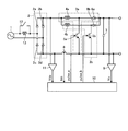
図1は、本実施の形態にかかる電力変換装置の構成例を示す図である。図1に示すように、電力変換装置は、単相整流器2と、チョッパ回路部3a,3bと、平滑コンデンサ7と、母線電流検出部8と、母線電圧検出部9と、スイッチング制御部10と、整流電圧検出部11と、交流開閉器12と、交流リアクタ13と、を備える。Embodiment 1 FIG.
FIG. 1 is a diagram illustrating a configuration example of the power conversion device according to the present embodiment. As shown in FIG. 1, the power conversion device includes a single-phase rectifier 2, chopper circuit units 3 a and 3 b, a smoothing capacitor 7, a bus current detection unit 8, a bus voltage detection unit 9, and a switching control unit 10. The rectified voltage detection unit 11, the AC switch 12, and the AC reactor 13 are provided.
図1は、本実施の形態にかかる電力変換装置の構成例を示す図である。図1に示すように、電力変換装置は、単相整流器2と、チョッパ回路部3a,3bと、平滑コンデンサ7と、母線電流検出部8と、母線電圧検出部9と、スイッチング制御部10と、整流電圧検出部11と、交流開閉器12と、交流リアクタ13と、を備える。
FIG. 1 is a diagram illustrating a configuration example of the power conversion device according to the present embodiment. As shown in FIG. 1, the power conversion device includes a single-
単相整流器(以下、単に「整流器」という)2は、4個の整流ダイオード2a~2dをブリッジ接続して構成され、単相交流電源(以下、単に「交流電源」という)1の交流電圧を整流する。チョッパ回路部3aは、リアクタ4aと、スイッチング素子5aと、逆流防止素子6aと、から構成される。チョッパ回路部3bは、リアクタ4bと、スイッチング素子5bと、逆流防止素子6bと、から構成される。図1に示すように、チョッパ回路部3aおよびチョッパ回路部3bは並列接続している。各スイッチング素子5a,5bは、例えば、IGBT(Insulated GATE Bipolar Transistor)により構成される。また、各逆流防止素子6a,6bは、例えば、ファストリカバリダイオードにより構成される。平滑コンデンサ7は、チョッパ回路部3a,3bの出力を平滑する。
The single-phase rectifier (hereinafter simply referred to as “rectifier”) 2 is configured by bridge-connecting four rectifier diodes 2a to 2d, and the AC voltage of the single-phase AC power source (hereinafter simply referred to as “AC power source”) 1 is supplied. Rectify. The chopper circuit unit 3a includes a reactor 4a, a switching element 5a, and a backflow prevention element 6a. The chopper circuit unit 3b includes a reactor 4b, a switching element 5b, and a backflow prevention element 6b. As shown in FIG. 1, the chopper circuit unit 3a and the chopper circuit unit 3b are connected in parallel. Each switching element 5a, 5b is comprised by IGBT (Insulated GATE Bipolar Transistor), for example. Moreover, each backflow prevention element 6a, 6b is comprised by a fast recovery diode, for example. The smoothing capacitor 7 smoothes the outputs of the chopper circuit units 3a and 3b.
母線電流検出部8は、整流器2から負荷(図示せず)へ流れ、負荷から整流器2に流れる電流である母線電流(Idc)を検出し、スイッチング制御部10に出力する。母線電圧検出部9は、チョッパ回路部3a,3bの出力電圧を平滑コンデンサ7で平滑した電圧である母線電圧(Vo)を検出し、スイッチング制御部10に出力する。スイッチング制御部10は、母線電流検出部8および母線電圧検出部9の各出力信号に基づいて、スイッチング素子5a,5bを動作させる駆動パルスを生成する制御手段である。整流電圧検出部11は、整流器2により整流された整流電圧(Vds)を検出し、スイッチング制御部10に出力する。
The bus current detector 8 flows from the rectifier 2 to the load (not shown), detects the bus current (Idc) that flows from the load to the rectifier 2, and outputs the detected bus current (Idc) to the switching controller 10. The bus voltage detection unit 9 detects a bus voltage (Vo), which is a voltage obtained by smoothing the output voltage of the chopper circuit units 3 a and 3 b with the smoothing capacitor 7, and outputs the detected voltage to the switching control unit 10. The switching control unit 10 is a control unit that generates drive pulses for operating the switching elements 5 a and 5 b based on the output signals of the bus current detection unit 8 and the bus voltage detection unit 9. The rectified voltage detector 11 detects the rectified voltage (Vds) rectified by the rectifier 2 and outputs it to the switching controller 10.
交流開閉器12は、交流電源1からの電源電流を交流リアクタ13に通過させるかバイパスするかを切り替える開閉器である。交流リアクタ13は、交流電源1からの高調波電流を抑制するリアクタである。図1に示すように、交流開閉器12および交流リアクタ13は、交流電源1と整流器2との間に配置され、並列に接続されている。
The AC switch 12 is a switch that switches whether the power source current from the AC power source 1 is passed through the AC reactor 13 or bypassed. The AC reactor 13 is a reactor that suppresses harmonic current from the AC power supply 1. As shown in FIG. 1, the AC switch 12 and the AC reactor 13 are arranged between the AC power source 1 and the rectifier 2 and connected in parallel.
なお、図1に示す例では、交流電源1が単相交流電源であり、整流器2を単相整流器とした構成例を示したが、一例であり、交流電源1が三相交流電源であり、整流器2を三相整流器とした構成であってもよい。また、図1に示す例では、チョッパ回路部を2個並列接続する構成例を示したが、一例であり、3個以上のチョッパ回路部を並列接続する構成であってもよい。
In the example illustrated in FIG. 1, the configuration example in which the AC power source 1 is a single-phase AC power source and the rectifier 2 is a single-phase rectifier is shown. However, the AC power source 1 is a three-phase AC power source. The rectifier 2 may be a three-phase rectifier. In the example illustrated in FIG. 1, a configuration example in which two chopper circuit units are connected in parallel is shown. However, the configuration is an example, and three or more chopper circuit units may be connected in parallel.
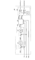
図2は、本実施の形態にかかる電力変換装置のスイッチング制御部の構成例を示す図である。図2に示すように、スイッチング制御部10は、母線電流指令値制御部21およびオンデューティ制御部22を具備したオンデューティ算出部20と、オンデューティ補正部23と、駆動パルス生成部24と、を備える。このスイッチング制御部10は、例えば、マイコンのような演算手段を用いて構成される。
FIG. 2 is a diagram illustrating a configuration example of the switching control unit of the power conversion device according to the present embodiment. As shown in FIG. 2, the switching control unit 10 includes an on-duty calculation unit 20 including a bus current command value control unit 21 and an on-duty control unit 22, an on-duty correction unit 23, a drive pulse generation unit 24, Is provided. The switching control unit 10 is configured using an arithmetic unit such as a microcomputer, for example.
母線電流指令値制御部21は、母線電圧検出部9の出力信号である母線電圧(Vo)と、例えば、予め設定される母線電圧指令値(Vo*)とから、母線電流指令値(Idc*)を演算する。この母線電流指令値(Idc*)の演算は、例えば、母線電圧検出部9の出力信号である母線電圧(Vo)と母線電圧指令値(Vo*)との差分を比例積分制御して行う。
The bus current command value control unit 21 generates a bus current command value (Idc *) from a bus voltage (Vo) that is an output signal of the bus voltage detection unit 9 and, for example, a preset bus voltage command value (Vo *). ) Is calculated. The calculation of the bus current command value (Idc *) is performed, for example, by proportional-integral control of the difference between the bus voltage (Vo) that is an output signal of the bus voltage detector 9 and the bus voltage command value (Vo *).
オンデューティ制御部22は、母線電流指令値制御部21により演算された母線電流指令値(Idc*)と母線電流検出部8により検出された母線電流(Idc)とから、各スイッチング素子5a,5bの基準オンデューティ(duty)を演算する。この基準オンデューティ(duty)の演算は、例えば、母線電流指令値制御部21の出力である母線電流指令値(Idc*)と母線電流検出部8の出力信号である母線電流(Idc)との差分を比例積分制御して行う。
The on-duty control unit 22 determines the switching elements 5a and 5b from the bus current command value (Idc *) calculated by the bus current command value control unit 21 and the bus current (Idc) detected by the bus current detection unit 8. The reference on-duty (duty) is calculated. The calculation of the reference on-duty (duty) is, for example, between a bus current command value (Idc *) that is an output of the bus current command value control unit 21 and a bus current (Idc) that is an output signal of the bus current detection unit 8. The difference is controlled by proportional integral control.
オンデューティ補正部23は、オンデューティ制御部22により演算された各スイッチング素子5a,5bの基準オンデューティ(duty)を補正して、スイッチング素子5aのオンデューティ(Daon)およびスイッチング素子5bのオンデューティ(Dbon)を生成する。
The on-duty correction unit 23 corrects the reference on-duty (duty) of the switching elements 5a and 5b calculated by the on-duty control unit 22, and the on-duty of the switching element 5a and the on-duty of the switching element 5b. (Dbon) is generated.
駆動パルス生成部24は、オンデューティ補正部23により生成された各オンデューティ(Daon,Dbon)に基づいて、各スイッチング素子5a,5bを動作させる駆動パルス(pulse_a,pulse_b)をそれぞれ生成して出力する。
The drive pulse generator 24 generates and outputs drive pulses (pulse_a, pulse_b) for operating the switching elements 5a, 5b based on the on-duties (Daon, Dbon) generated by the on-duty correction unit 23, respectively. To do.
ここで、母線電流指令値制御部21、オンデューティ制御部22での演算に用いる制御パラメータは、例えば、オンデューティ制御部22における比例制御ゲインが母線電圧に反比例して変化するのが望ましいなど、回路の動作状況に合わせた最適値が存在する。したがって、整流器2の出力電圧である整流電圧、母線電流(Idc)、母線電圧(Vo)の値に応じた計算式、もしくはテーブルを設け、回路の動作状況に合わせて制御パラメータを調整するようにしてもよい。これにより、スイッチング制御部10では、制御性を向上することができる。
Here, the control parameter used for the calculation in the bus current command value control unit 21 and the on-duty control unit 22 is preferably, for example, that the proportional control gain in the on-duty control unit 22 changes in inverse proportion to the bus voltage. There is an optimum value according to the operation status of the circuit. Therefore, a calculation formula or a table corresponding to the values of the rectified voltage, the bus current (Idc), and the bus voltage (Vo), which are output voltages of the rectifier 2, is provided, and the control parameters are adjusted according to the operation state of the circuit. May be. Thereby, in the switching control part 10, controllability can be improved.
また、母線電流指令値制御部21、オンデューティ制御部22での演算手法として比例積分制御を挙げたが、演算手法はこれらの制御演算手法に限定するものではなく、微分項を追加して比例積分微分制御とするなど、その他の演算手法を用いてもよい。また、母線電流指令値制御部21、オンデューティ制御部22での演算手法を同一の手法とする必要もなく、異なる手法を用いてもよい。
Moreover, although proportional integral control was mentioned as a calculation method in the bus current command value control unit 21 and the on-duty control unit 22, the calculation method is not limited to these control calculation methods. Other calculation methods such as integral / differential control may be used. Moreover, it is not necessary to use the same calculation method in the bus current command value control unit 21 and the on-duty control unit 22, and different methods may be used.
ここで、オンデューティ補正部23の動作を、各チョッパ回路部3a,3bの動作と合わせて説明する。ここでは、まず、チョッパ回路部3aのスイッチング素子5aをオン/オフした場合の挙動について説明する。チョッパ回路部3aには、整流器2の出力である整流電圧(Vds)が入力され、チョッパ回路部3aの出力が平滑コンデンサ7で平滑され、母線電圧(Vo)が得られる。チョッパ回路部3aにおいて、スイッチング素子5aがオンしたとき、逆流防止素子6aの導通が阻止され、リアクタ4aには整流電圧(Vds)が印加される。一方、スイッチング素子5aがオフしたとき、逆流防止素子6aが導通し、リアクタ4aには、整流電圧(Vds)と母線電圧(Vo)との差分の電圧が、スイッチング素子5aがオンしたときとは逆向きに誘導される。このとき、スイッチング素子5aのオン時にリアクタ4aに蓄積されたエネルギーが、スイッチング素子5のオフ時に負荷へ移送されると見ることができる。スイッチング素子5aのオン/オフ時に、リアクタ4aを出入りするエネルギーが等しいとすると、スイッチング素子5aのオンデューティ(Daon)、整流電圧(Vds)、および母線電圧(Vo)の関係は、下記(1)式で表される。
Here, the operation of the on-duty correction unit 23 will be described together with the operations of the chopper circuit units 3a and 3b. Here, first, the behavior when the switching element 5a of the chopper circuit portion 3a is turned on / off will be described. A rectified voltage (Vds) that is an output of the rectifier 2 is input to the chopper circuit unit 3a, and an output of the chopper circuit unit 3a is smoothed by the smoothing capacitor 7 to obtain a bus voltage (Vo). In the chopper circuit portion 3a, when the switching element 5a is turned on, conduction of the backflow prevention element 6a is blocked, and a rectified voltage (Vds) is applied to the reactor 4a. On the other hand, when the switching element 5a is turned off, the backflow prevention element 6a becomes conductive, and the reactor 4a has a difference voltage between the rectified voltage (Vds) and the bus voltage (Vo) when the switching element 5a is turned on. Guided in the opposite direction. At this time, it can be seen that the energy stored in the reactor 4a when the switching element 5a is turned on is transferred to the load when the switching element 5 is turned off. Assuming that the energy entering and exiting the reactor 4a is equal when the switching element 5a is turned on / off, the relationship between the on-duty (Daon), the rectified voltage (Vds), and the bus voltage (Vo) of the switching element 5a is as follows: It is expressed by a formula.
Vo=Vds/(1-Daon) …(1)
Vo = Vds / (1-Daon) ... (1)
上記(1)式から明らかなように、スイッチング素子5aのオンデューティ(Daon)を制御することで、チョッパ回路部3aの出力電圧、すなわち母線電圧(Vo)を制御することができる。
As is clear from the above equation (1), the output voltage of the chopper circuit portion 3a, that is, the bus voltage (Vo) can be controlled by controlling the on-duty (Daon) of the switching element 5a.
つぎに、チョッパ回路部3aにおいてリアクタ4aに流れるリアクタ電流(ILaon)とオンデューティ(Daon)との関係について説明する。スイッチング素子5aがオンしている場合、上述したように、リアクタ4aには整流電圧(Vds)が印加される。このとき、リアクタ4aを交流電源1側から負荷側に流れるリアクタ電流(ILa)は、直線的に増加する。このときのリアクタ4aに流れるリアクタ電流をILaonとし、リアクタ4aのインダクタンス値をLaとすると、このILaonの傾きΔILaonは、下記(2)式で表される。
Next, the relationship between the reactor current (ILaon) flowing through the reactor 4a in the chopper circuit unit 3a and the on-duty (Daon) will be described. When the switching element 5a is on, the rectified voltage (Vds) is applied to the reactor 4a as described above. At this time, the reactor current (ILa) flowing through the reactor 4a from the AC power supply 1 side to the load side increases linearly. When the reactor current flowing through the reactor 4a at this time is ILaon and the inductance value of the reactor 4a is La, the slope ΔILaon of this ILaon is expressed by the following equation (2).
ΔILaon=Vds/La …(2)
ΔILaon = Vds / La (2)
また、スイッチング素子5aがオフしているとき、つまり、駆動パルス(pulse_a)が「L」である期間は、上述したように、リアクタ4aには整流電圧(Vds)と母線電圧(Vo)との差分の電圧が、スイッチング素子5aのオン時とは逆向きに印加され、リアクタ4aを交流電源1側から負荷側に流れるリアクタ電流(ILa)は、直線的に減少する。このときのリアクタ4aに流れるリアクタ電流をILaoffとすると、このILaoffの傾きΔILaoffは、下記(3)式で表される。
Further, when the switching element 5a is off, that is, during the period when the drive pulse (pulse_a) is “L”, the reactor 4a receives the rectified voltage (Vds) and the bus voltage (Vo) as described above. The difference voltage is applied in the opposite direction to that when the switching element 5a is turned on, and the reactor current (ILa) flowing through the reactor 4a from the AC power supply 1 side to the load side decreases linearly. If the reactor current flowing through the reactor 4a at this time is ILaoff, the slope ΔILaoff of this ILaoff is expressed by the following equation (3).
ΔILaoff=(Vds-Vo)/La …(3)
ΔILaoff = (Vds−Vo) / La (3)
同様にして、スイッチング素子5bのオンデューティ(Dbon)、整流電圧(Vds)、および母線電圧(Vo)の関係は下記(4)式で表される。
Similarly, the relationship between the on-duty (Dbon), the rectified voltage (Vds), and the bus voltage (Vo) of the switching element 5b is expressed by the following equation (4).
Vo=Vds/(1-Dbon) …(4)
Vo = Vds / (1-Dbon) ... (4)
また、スイッチング素子5bがオンしている場合、リアクタ4bを交流電源1側から負荷側に流れるリアクタ電流(ILb)は、直線的に増加する。このときのリアクタ4bに流れるリアクタ電流をILbonとし、リアクタ4bのインダクタンス値をLbとすると、このILbonの傾きΔILbonは、下記(5)式で表される。
Further, when the switching element 5b is on, the reactor current (ILb) flowing through the reactor 4b from the AC power supply 1 side to the load side increases linearly. When the reactor current flowing through the reactor 4b at this time is ILbon and the inductance value of the reactor 4b is Lb, the slope ΔILbon of the ILbon is expressed by the following equation (5).
ΔILbon=Vds/Lb …(5)
ΔILbon = Vds / Lb (5)
また、スイッチング素子5bがオフしている場合、リアクタ4bを交流電源1側から負荷側に流れるリアクタ電流(ILb)は、直線的に減少する。このときのリアクタ電流をILboffとすると、このILboffの傾きΔILboffは、下記(6)式で表される。
Further, when the switching element 5b is off, the reactor current (ILb) flowing through the reactor 4b from the AC power supply 1 side to the load side decreases linearly. Assuming that the reactor current at this time is ILboff, the slope ΔILboff of this ILboff is expressed by the following equation (6).
ΔILboff=(Vds-Vo)/Lb …(6)
ΔILboff = (Vds−Vo) / Lb (6)
各スイッチング素子5a,5bの各オンデューティ(Daon,Dbon)は、上述したように、スイッチング制御部10において、母線電圧(Vo)、整流電圧(Vds)、リアクタ電流(ILa)、およびリアクタ電流(ILb)を用いて算出することができる。ここで、各スイッチング素子5a,5bの各オン期間が重ならない区間では、母線電流検出部8により検出される母線電流(Idc)は、(ILaon+ILboff)、または、(ILaoff+ILbon)に等しい値となる。つまり、母線電流検出部8により検出される母線電流(Idc)を用いて、各スイッチング素子5a,5bの各オンデューティ(Daon,Dbon)を算出することができる。
As described above, the on-duty (Daon, Dbon) of each switching element 5a, 5b is determined in the switching control unit 10 by the bus voltage (Vo), the rectified voltage (Vds), the reactor current (ILa), and the reactor current ( ILb). Here, the bus current (Idc) detected by the bus current detector 8 is equal to (ILaon + ILboff) or (ILaoff + ILbon) in a section where the ON periods of the switching elements 5a and 5b do not overlap. That is, the on-duty (Daon, Dbon) of each switching element 5a, 5b can be calculated using the bus current (Idc) detected by the bus current detector 8.
本実施の形態では、スイッチング制御部10は、例えば、図1に示す例では、各スイッチング素子5a,5bのスイッチング周期において、スイッチング素子5aのオンタイミングに対し、スイッチング素子5bのオンタイミングの位相が半周期(180(=360/2)°)遅れるように制御する。これにより、リアクタ電流(ILa)およびリアクタ電流(ILb)の加算電流である母線電流(Idc)の各スイッチング素子5a,5bのスイッチングに起因するリプルが相殺される。例えば、n個のチョッパ回路部を並列接続して本実施の形態にかかる電力変換装置を構成した場合には、各チョッパ回路部のスイッチング素子のスイッチングの位相差を(360/n)°とすれば、母線電流(Idc)のリプルを最小とすることができる。なお、この複数のチョッパ回路部における各スイッチング素子のスイッチングの位相差は一例であり、このような方法に限定するものではなく、他の方法を用いて複数のチョッパ回路部における各スイッチング素子のスイッチングの位相差を決定してもよい。
In the present embodiment, for example, in the example shown in FIG. 1, the switching control unit 10 is configured such that the on-timing phase of the switching element 5 b is different from the on-timing of the switching element 5 a in the switching cycle of the switching elements 5 a and 5 b. Control is performed so as to be delayed by a half cycle (180 (= 360/2) °). Thereby, the ripple resulting from switching of each switching element 5a, 5b of bus current (Idc) which is the addition current of reactor current (ILa) and reactor current (ILb) is canceled. For example, when the power converter according to the present embodiment is configured by connecting n chopper circuit units in parallel, the switching phase difference of the switching elements of each chopper circuit unit is set to (360 / n) °. For example, the ripple of the bus current (Idc) can be minimized. Note that the switching phase difference of each switching element in the plurality of chopper circuit units is an example, and is not limited to such a method, and the switching of each switching element in the plurality of chopper circuit units using other methods. The phase difference may be determined.
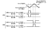
つぎに、オンタイミングの位相が半周期(180°)異なるように、各スイッチング素子5a,5bの各駆動パルス(pulse_a,pulse_b)を生成する手法の一例について説明する。図3は、本実施の形態にかかる電力変換装置のキャリア信号とタイマ値との関係および各駆動パルスの各波形を示す図である。
Next, an example of a method for generating the drive pulses (pulse_a, pulse_b) of the switching elements 5a and 5b so that the phase of the on-timing is different by a half cycle (180 °) will be described. FIG. 3 is a diagram showing a relationship between the carrier signal and the timer value and each waveform of each drive pulse of the power conversion device according to the present embodiment.
スイッチング制御部10において、駆動パルス生成部24は、三角波のキャリア信号と、各スイッチング素子5a,5bの各オンデューティ(Daon,Dbon)に対応した各タイマ値α,βとを比較し、その比較結果の大小に応じて、各スイッチング素子5a,5bの各駆動パルス(pulse_a,pulse_b)を生成する。
In the switching control unit 10, the drive pulse generation unit 24 compares the triangular wave carrier signal with each timer value α, β corresponding to each on-duty (Daon, Dbon) of each switching element 5a, 5b, and compares the comparison. Depending on the magnitude of the result, each drive pulse (pulse_a, pulse_b) of each switching element 5a, 5b is generated.
例えば、図3に示すように、一方のスイッチング素子(ここでは、スイッチング素子5a)のオンデューティ(Daon)に対応するタイマ値αを基準として、他方のスイッチング素子(ここでは、スイッチング素子5b)のオンデューティ(Dbon)に対応するタイマ値βを、1(キャリア信号の大きさを「1」とする)から一方のスイッチング素子(ここでは、スイッチング素子5a)のオンデューティ(Daon)に対応するタイマ値αを差し引いた値(1-α)とする。三角波のキャリア信号と、Daonに対応したタイマ値αおよびDbonに対応したタイマ値β(=1-α)と、をそれぞれ比較する。
For example, as shown in FIG. 3, the timer value α corresponding to the on-duty (Daon) of one switching element (here switching element 5a) is used as a reference for the other switching element (here switching element 5b). The timer value β corresponding to the on-duty (Dbon) is changed from 1 (the magnitude of the carrier signal is “1”) to the timer corresponding to the on-duty (Daon) of one switching element (here, the switching element 5a). The value (1-α) is obtained by subtracting the value α. The triangular wave carrier signal is compared with the timer value α corresponding to Daon and the timer value β (= 1−α) corresponding to Dbon.
そして、駆動パルス生成部24は、キャリア信号よりもDaonに対応したタイマ値αが大きい場合に「High」、キャリア信号よりもDaonに対応したタイマ値αが小さい場合に「Low」となるスイッチング素子5aの駆動パルス(pulse_a)を生成する。また、駆動パルス生成部24は、キャリア信号よりもDbonに対応したタイマ値β(=1-α)が大きい場合に「Low」、キャリア信号よりもDbonに対応したタイマ値β(=1-α)が小さい場合に「High」となるスイッチング素子5bの駆動パルス(pulse_b)を生成する。このように駆動パルスを生成することで、オンタイミングの位相が180°異なり、オン期間が等しい(Taon=Tbon)スイッチング素子5aの駆動パルス(pulse_a)およびスイッチング素子5bの駆動パルス(pulse_b)が得られる。
The drive pulse generator 24 is “High” when the timer value α corresponding to Daon is larger than the carrier signal, and “Low” when the timer value α corresponding to Daon is smaller than the carrier signal. A drive pulse (pulse_a) 5a is generated. The drive pulse generator 24 is “Low” when the timer value β (= 1−α) corresponding to Dbon is larger than the carrier signal, and the timer value β (= 1−α) corresponding to Dbon than the carrier signal. ) Is small, the drive pulse (pulse_b) of the switching element 5b which becomes “High” is generated. By generating the drive pulse in this manner, the drive pulse (pulse_a) of the switching element 5a and the drive pulse (pulse_b) of the switching element 5b are obtained, which are different in ON timing phase by 180 ° and have the same ON period (Taon = Tbon). It is done.
なお、各駆動パルス(pulse_a,pulse_b)を生成する際のキャリア信号と各タイマ値α,βとの大小と各駆動パルス(pulse_a,pulse_b)の「High」、「Low」との関係は、上述した例に限らず、各オンデューティ(Daon,Dbon)と各駆動パルス(pulse_a,pulse_b)の各オン期間(Taon,Tbon)との関係が一致していればよい。
The relationship between the magnitude of the carrier signal and the timer values α and β when generating each drive pulse (pulse_a, pulse_b) and “High” and “Low” of each drive pulse (pulse_a, pulse_b) is described above. The relationship between each on-duty (Daon, Dbon) and each on-duration (Taon, Tbon) of each drive pulse (pulse_a, pulse_b) is not limited to this example.
例えば、モータ制御などに使われる汎用のマイコンには、三相インバータの相補PWM(Pulse Width Modulation)を生成する機能を持つものがある。この三相インバータの各スイッチング素子のオンデューティに対応したタイマ値に基づき、各相の上下のスイッチング素子の駆動パルスを生成する場合に、上述したように位相が半周期異なる2つの駆動パルスを生成する場合、この三相インバータの相補PWMの生成機能を用いてもよい。図4は、三相インバータの相補PWM生成機能を用いた際のキャリア信号とタイマ値との関係および各駆動パルスの各波形を示す図である。
For example, some general-purpose microcomputers used for motor control have a function of generating complementary PWM (Pulse Width Modulation) of a three-phase inverter. Based on the timer value corresponding to the on-duty of each switching element of this three-phase inverter, when generating driving pulses for the upper and lower switching elements of each phase, as described above, two driving pulses with different phases by half cycle are generated. In this case, the complementary PWM generation function of this three-phase inverter may be used. FIG. 4 is a diagram showing a relationship between a carrier signal and a timer value and each waveform of each drive pulse when the complementary PWM generation function of the three-phase inverter is used.
図4に示すように、三相インバータの相補PWM生成機能を用いた場合、三相のうちの任意の二相のタイマ値を、上述したα,β(=1-α)の関係を用いて設定すれば、一方の相(図4に示す例ではA相)のアームの上側(あるいは下側)のスイッチング素子のオンデューティ(Daon)に対応したタイマ値αに基づいて生成された上側(あるいは下側)のスイッチング素子用の駆動パルスと、他方の相(図4に示す例ではB相)のアームの下側(あるいは上側)のスイッチング素子のオンデューティ(Dbon)に対応したタイマ値β(=1-α)に基づいて生成された下側(あるいは上側)のスイッチング素子用の駆動パルスとは、位相が半周期異なる関係となる。この三相インバータの相補PWMを生成する機能を用いることにより、各駆動パルスを生成する際のキャリア信号と各タイマ値との大小と各駆動パルスの「High」、「Low」との条件を変更することなく、ソフトウェア上においてタイマ値を設定すれば、位相が半周期異なる関係の駆動パルスを簡易に生成することができる。
As shown in FIG. 4, when the complementary PWM generation function of the three-phase inverter is used, an arbitrary two-phase timer value of the three phases is calculated using the relationship of α and β (= 1−α) described above. If set, the upper side (or the upper side) generated based on the timer value α corresponding to the on-duty (Daon) of the switching element on the upper side (or lower side) of the arm of one phase (A phase in the example shown in FIG. 4) A driving pulse for the lower switching element and a timer value β (corresponding to the on-duty (Dbon) of the lower (or upper) switching element of the arm of the other phase (B phase in the example shown in FIG. 4). = 1−α), the phase is different from the driving pulse for the lower (or upper) switching element by a half cycle. By using the function to generate complementary PWM of this three-phase inverter, the size of the carrier signal and each timer value when generating each drive pulse and the conditions of “High” and “Low” of each drive pulse are changed. If a timer value is set on the software without doing so, it is possible to easily generate drive pulses having a phase difference of half a cycle.
ここで、各チョッパ回路部3a,3bにおいて、各スイッチング素子5a,5bのオンデューティ(Daon,Dbon)が同値であっても、各スイッチング素子5a,5bのオンタイミングの位相差による整流電圧(Vds)の誤差、各リアクタ4a,4bの各インダクタンス値La,Lbのバラツキなどにより、上述した(2)、(3)、(5)、および(6)式に示した各スイッチング素子5a,5bのオンタイミング時の傾き(ΔILaon,ΔILbon)およびオフタイミング時の傾き(ΔILaoff,ΔILboff)が異なる値となり、各スイッチング素子5a,5bの各オン期間における母線電流(Idc)の変化量にアンバランスが生じ、母線電流(Idc)に歪みを発生させ、入力電流の高調波成分が増加する。
Here, in each chopper circuit part 3a, 3b, even if the on-duty (Daon, Dbon) of each switching element 5a, 5b is the same value, the rectified voltage (Vds) due to the phase difference of the on-timing of each switching element 5a, 5b. ), And variations in the inductance values La and Lb of the reactors 4a and 4b, etc., the switching elements 5a and 5b shown in the expressions (2), (3), (5), and (6) described above. The slopes at the ON timing (ΔILaon, ΔILbon) and the slopes at the OFF timing (ΔILaoff, ΔILboff) are different values, and an unbalance occurs in the amount of change in the bus current (Idc) in each ON period of each switching element 5a, 5b. The bus current (Idc) is distorted, and the harmonic component of the input current increases.
そこで、本実施の形態では、オンデューティ補正部23において、母線電流(Idc)および母線電圧(Vo)を用いて母線電流指令値制御部21およびオンデューティ制御部22により演算した基準オンデューティ(duty)を、各チョッパ回路部3a,3bにおける各スイッチング素子5a,5bのオンタイミングの位相差による整流電圧(Vds)の誤差、リアクタ4a,4bのインダクタンス値La,Lbのバラツキに応じて、それぞれ各チョッパ回路部3a,3bに好適なオンデューティに補正する。これにより、上述したような入力電流の高調波成分の増加を抑制することができる。
Therefore, in the present embodiment, in the on-duty correction unit 23, the reference on-duty (duty) calculated by the bus current command value control unit 21 and the on-duty control unit 22 using the bus current (Idc) and the bus voltage (Vo). ) According to the error of the rectified voltage (Vds) due to the phase difference of the on-timing of the switching elements 5a and 5b in the chopper circuit portions 3a and 3b, and the variations in the inductance values La and Lb of the reactors 4a and 4b, respectively. Correction is made to an on-duty suitable for the chopper circuit portions 3a and 3b. Thereby, the increase in the harmonic component of the input current as described above can be suppressed.
つづいて、上記で説明した電力変換装置を備えたモータ駆動制御装置について説明する。図5は、本実施の形態にかかる電力変換装置を備えたモータ駆動制御装置の構成例を示す図である。上述の電力変換装置に負荷を接続した状態を示すものである。図5に示す例では、電力変換装置30は図1に示す電力変換装置である。電力変換装置30の負荷として、直流電圧を交流電圧に変換するインバータ31と、インバータ31の出力である交流電圧が印加されることで駆動するモータ32とを接続した負荷を示している。
Next, a motor drive control device including the power conversion device described above will be described. FIG. 5 is a diagram illustrating a configuration example of a motor drive control device including the power conversion device according to the present embodiment. The state which connected the load to the above-mentioned power converter device is shown. In the example illustrated in FIG. 5, the power conversion device 30 is the power conversion device illustrated in FIG. 1. As a load of the power conversion device 30, a load in which an inverter 31 that converts a DC voltage into an AC voltage and a motor 32 that is driven by applying an AC voltage that is an output of the inverter 31 are shown.
インバータ31は、例えば、IGBTのようなスイッチング素子を三相ブリッジ構成もしくは二相ブリッジ構成とする。インバータ31を制御するインバータ制御部33は、例えば、インバータ31からモータ32に流れる電流を検出するモータ電流検出部34を用いて、モータ32が所望の回転数にて回転するような電圧指令を演算して、インバータ31内のスイッチング素子を駆動するパルスを生成する。
The inverter 31 has, for example, a switching element such as an IGBT having a three-phase bridge configuration or a two-phase bridge configuration. The inverter control unit 33 that controls the inverter 31 uses, for example, a motor current detection unit 34 that detects a current flowing from the inverter 31 to the motor 32 to calculate a voltage command that causes the motor 32 to rotate at a desired rotational speed. Thus, a pulse for driving the switching element in the inverter 31 is generated.
また、図5に示す構成において、インバータ制御部33によるインバータ制御は、スイッチング制御部10と同様に、例えば、マイコンのような演算手段を用いて実現すればよい。
In addition, in the configuration shown in FIG. 5, the inverter control by the inverter control unit 33 may be realized by using an arithmetic means such as a microcomputer, for example, similarly to the switching control unit 10.
また、電力変換装置30において、図5に示す負荷が接続されて構成されるモータ駆動制御装置では、電力変換装置30への電力負荷に応じて、必要な母線電圧(Vo)が異なるという特色がある。
Further, in the power conversion device 30, the motor drive control device configured by connecting the load shown in FIG. 5 has a feature that the required bus voltage (Vo) varies depending on the power load to the power conversion device 30. is there.
一般に、モータ32の回転数が高回転になるほど、インバータ31からの出力電圧は高くする必要があるが、このインバータ31からの出力電圧の上限は、インバータ31への入力電圧、つまり、電力変換装置30の出力である母線電圧(Vo)により制限される。インバータ31からの出力電圧が、母線電圧(Vo)により制限された上限を超えて飽和する領域を過変調領域と呼ぶ。
Generally, the higher the rotational speed of the motor 32, the higher the output voltage from the inverter 31. The upper limit of the output voltage from the inverter 31 is the input voltage to the inverter 31, that is, the power converter. It is limited by the bus voltage (Vo) which is 30 outputs. A region where the output voltage from the inverter 31 saturates beyond the upper limit limited by the bus voltage (Vo) is called an overmodulation region.
このようなモータ駆動制御装置においては、モータ32が低回転である(過変調領域に到達しない)範囲では、母線電圧(Vo)を昇圧する必要はなく、モータ32が高回転となった場合には、母線電圧(Vo)を昇圧することで、過変調領域をより高回転側にすることができる。これにより、モータ32の運転範囲を高回転側に拡大できる。
In such a motor drive control device, it is not necessary to increase the bus voltage (Vo) in a range where the motor 32 is at a low rotation (not reaching the overmodulation region), and when the motor 32 is at a high rotation. Can boost the overmodulation region to the higher rotation side by boosting the bus voltage (Vo). Thereby, the operating range of the motor 32 can be expanded to the high rotation side.
また、モータ32の運転範囲を拡大する必要がなければ、その分モータ32の固定子巻線を高巻数化することができる。このとき、低回転数の領域では、モータ電圧が高くなる分、電流が少なくなり、インバータ31での損失低減が見込まれる。モータ32の運転範囲拡大と低回転数領域の損失改善の双方の効果を得るため、モータ32の高巻数化の程度を適切に設計してもよい。
Further, if it is not necessary to expand the operation range of the motor 32, the number of turns of the stator winding of the motor 32 can be increased accordingly. At this time, in the low rotation speed region, the current decreases as the motor voltage increases, and loss reduction in the inverter 31 is expected. In order to obtain the effects of both expanding the operating range of the motor 32 and improving the loss in the low rotation speed region, the degree of increase in the number of turns of the motor 32 may be appropriately designed.
また、上述した電力変換装置30を適用したモータ駆動制御装置を、送風機または圧縮機のモータの少なくとも1つを駆動するために用いて空気調和機を構成した場合においても、同様の効果が得られる。図6は、モータ駆動制御装置を備えた空気調和機の構成例を示す図である。室外ユニット40は、図5に示すモータ駆動制御装置41と、送風機42と、圧縮機43と、を備え、室内ユニット50とともに空気調和機を構成する。モータ駆動制御装置41は、送風機42に使用されるモータ、または圧縮機43に使用されるモータ、の少なくとも一方のモータについて、上述のモータ駆動制御を行う。なお、図6では、概観の概念を示しているため、配線等を図示していないが、モータ駆動制御装置41は、送風機42、圧縮機43と配線等により接続されている。
Further, the same effect can be obtained even when an air conditioner is configured by using the motor drive control device to which the above-described power conversion device 30 is applied to drive at least one of a motor of a blower or a compressor. . FIG. 6 is a diagram illustrating a configuration example of an air conditioner including a motor drive control device. The outdoor unit 40 includes a motor drive control device 41, a blower 42, and a compressor 43 shown in FIG. 5, and constitutes an air conditioner together with the indoor unit 50. The motor drive control device 41 performs the motor drive control described above for at least one of the motor used for the blower 42 or the motor used for the compressor 43. In addition, in FIG. 6, since the concept of the overview is shown, wiring and the like are not shown, but the motor drive control device 41 is connected to the blower 42 and the compressor 43 by wiring and the like.
つづいて、電力変換装置をモータ駆動制御装置に適用した場合において、駆動するモータの低速運転条件における、高効率化のための動作について説明する。図1において、交流開閉器12は、励磁した状態でオンとなるa接点型電磁開閉器とし、交流リアクタ13は、鋼板コアを用いた商用電源用帯域の低周波交流リアクタとする。また、ここでは、電力変換装置の負荷は、インバータによる可変速型の空気調和機用の圧縮機とし、空気調和機に適用した場合について説明する。
Next, the operation for increasing the efficiency under the low speed operation condition of the motor to be driven when the power conversion device is applied to the motor drive control device will be described. In FIG. 1, an AC switch 12 is an a-contact type electromagnetic switch that is turned on in an excited state, and an AC reactor 13 is a commercial frequency band low-frequency AC reactor using a steel plate core. In addition, here, a description will be given of a case where the load of the power conversion device is a compressor for a variable speed type air conditioner using an inverter and applied to the air conditioner.
空調負荷が小さく、出力が所定の出力以下の場合、具体的には、インバータによる圧縮機の年間運転率の高い冷暖房の中間運転条件に相当する最大出力の1/10以下の出力において、電力変換装置では、交流開閉器12は励磁電流を流さない接点を開いた状態で、電源電流は交流リアクタ13を通過する。交流リアクタ13は、中間運転条件で磁気飽和なく、かつ、スイッチング素子5a,5bがスイッチングしないパッシブ条件で電源高調波電流を抑制できる1~15mHとする。これにより、電力変換装置では、スイッチング素子5a,5bのスイッチングに起因して発生する、スイッチング素子5a,5bの定常損失およびスイッチング損失、逆流防止素子6a,6bのリカバリ損失、リアクタ4a,4bの高周波鉄損がゼロになり、コンバータ損失を低減できる。特に、年間運転率の高い条件で損失を低減できるので、空調機全体の省エネに大きく寄与する。さらに、交流開閉器12をa接点型電磁開閉器としたことで、中間運転条件における交流開閉器12(電磁開閉器)の励磁に伴う損失もゼロ化できる。
When the air conditioning load is small and the output is less than or equal to a predetermined output, specifically, power conversion is performed at an output of 1/10 or less of the maximum output corresponding to the intermediate operation condition of air conditioning with a high annual operation rate of the compressor by the inverter. In the apparatus, the AC switch 12 is in a state in which a contact that does not pass an exciting current is opened, and the power source current passes through the AC reactor 13. The AC reactor 13 is set to 1 to 15 mH that can suppress the power supply harmonic current under the passive condition in which the switching elements 5a and 5b are not switched under the intermediate operation condition and without the magnetic saturation. Thus, in the power conversion device, the steady loss and switching loss of the switching elements 5a and 5b, the recovery loss of the backflow prevention elements 6a and 6b, and the high frequency of the reactors 4a and 4b, which are generated due to the switching of the switching elements 5a and 5b. Iron loss becomes zero, and converter loss can be reduced. In particular, the loss can be reduced under conditions with a high annual operating rate, thus greatly contributing to energy saving of the entire air conditioner. Furthermore, the loss associated with the excitation of the AC switch 12 (electromagnetic switch) under intermediate operating conditions can be reduced to zero by using the a contact type electromagnetic switch as the AC switch 12.
一方、空調負荷が大きく、インバータによる圧縮機が高出力条件の場合、具体的には、最大出力の1/10よりも大きい出力において、電力変換装置では、交流開閉器12の接点を閉じ、交流リアクタ13をバイパスし、スイッチング素子5a,5bのスイッチングにより電流制御を行い、電源高調波電流を抑制する。交流リアクタ13をバイパスすることで、高出力時の高電流による交流リアクタ13の飽和による電流制御の不安定性を回避する。また、このような構成としたことで、交流リアクタ13は、中間運転条件の低周波かつ低電流定格の交流リアクタでよいので、低コストに抑えることができる。また、交流開閉器12について、一般的に直流開閉器に対して低コストの交流開閉器を用いることができる。このような交流リアクタ13および交流開閉器12を用いることで、高周波スイッチングコンバータを搭載した空調機の中間運転条件における効率改善に対して最小コストで実現可能となる。
On the other hand, when the air conditioning load is large and the compressor by the inverter is in a high output condition, specifically, at an output greater than 1/10 of the maximum output, the power converter closes the contact of the AC switch 12 to The reactor 13 is bypassed, current control is performed by switching the switching elements 5a and 5b, and the power harmonic current is suppressed. By bypassing the AC reactor 13, instability of current control due to saturation of the AC reactor 13 due to high current at high output is avoided. In addition, with such a configuration, the AC reactor 13 may be an AC reactor having a low frequency and a low current rating under intermediate operation conditions, so that the cost can be reduced. Further, as the AC switch 12, a low-cost AC switch can be generally used for the DC switch. By using the AC reactor 13 and the AC switch 12 as described above, it is possible to realize efficiency improvement in an intermediate operation condition of an air conditioner equipped with a high frequency switching converter at a minimum cost.
さらに、電力変換装置では、交流開閉器12(電磁開閉器)が経年故障モードで接点溶着した場合に、これを検知して、中間運転条件にもスイッチング素子5a,5bのスイッチングによる電流制御により高調波電流を抑制することができる。これにより、効率は低下するものの、空調機の機能は維持され、寿命の長い電力変換装置および空気調和機を得ることができる。
Further, in the power converter, when the AC switch 12 (electromagnetic switch) is welded in contact in the aging failure mode, this is detected, and the intermediate operation condition is also controlled by current control by switching of the switching elements 5a and 5b. Wave current can be suppressed. Thereby, although efficiency falls, the function of an air conditioner is maintained and the power converter device and air conditioner with a long lifetime can be obtained.
接点溶着の検知方法については、母線電流検出部8が、スイッチング素子5a,5bのスイッチング停止時に電源高調波電流の有無を検知して判断を行う。交流開閉器12、スイッチング素子5a,5b、および空調機用インバータを1つのマイコンで制御すれば、本運転継続機能はS/Wのみで実現でき、追加コストは不要である。さらに、1つのマイコンで制御することで、接点が開いた状態および閉じた状態での電流、モータの制御ゲインを調整することもS/Wの変更のみででき、接点切り替え時にモータを連続動作させることができる。これにより、接点条件切り替え時の運転・停止による冷媒回路の損失低減、温度変化による不快感を軽減できる、空気調和機を得ることができる。
About the detection method of contact welding, the bus current detection part 8 detects the presence or absence of a power supply harmonic current at the time of switching stop of switching element 5a, 5b, and makes a determination. If the AC switch 12, the switching elements 5a and 5b, and the inverter for the air conditioner are controlled by a single microcomputer, the operation continuation function can be realized only by S / W, and no additional cost is required. Furthermore, by controlling with one microcomputer, it is possible to adjust the current when the contacts are open and closed, and the control gain of the motor only by changing the S / W, and the motor is operated continuously when switching the contacts. be able to. Thereby, the air conditioner which can reduce the loss of the refrigerant circuit by the driving | operation / stop at the time of contact condition switching, and can reduce the discomfort by a temperature change can be obtained.
さらに、電力変換装置では、高調波電流を交流リアクタ13で抑制することにより、中間運転条件時の無効電流が抑制されることから、逆流防止素子6a,6bの定常損失、リアクタ4a,4bの銅損も低減できる。
Furthermore, in the power converter, since the harmonic current is suppressed by the AC reactor 13, the reactive current during the intermediate operation condition is suppressed. Therefore, the steady loss of the backflow prevention elements 6a and 6b, the copper of the reactors 4a and 4b, Loss can also be reduced.
以上説明したように、本実施の形態によれば、電力変換装置では、交流電源と整流器との間に、交流開閉器と、交流開閉器に並列に接続された交流リアクタと、を備え、負荷としてモータを駆動するインバータと接続してモータ駆動制御回路を構成する場合に、モータの駆動状態に応じて交流開閉器の開閉を制御することとした。これにより、簡易な構成で、接続した負荷の動作モードによらずに交流電源からの高調波電流を抑制することができ、また、モータ接続時において低速動作時での各素子における損失を低減することができる。
As described above, according to the present embodiment, the power conversion device includes an AC switch and an AC reactor connected in parallel to the AC switch between the AC power source and the rectifier, and a load. When the motor drive control circuit is configured by connecting to an inverter that drives the motor, the opening / closing of the AC switch is controlled according to the driving state of the motor. As a result, the harmonic current from the AC power supply can be suppressed with a simple configuration regardless of the operation mode of the connected load, and the loss in each element during low-speed operation when the motor is connected is reduced. be able to.
実施の形態2.
図7は、本実施の形態にかかる電力変換装置の構成例を示す図である。実施の形態1の構成(図1参照)に、直流開閉器14を追加したものである。直流開閉器14は、チョッパ回路部3a,3bに対して並列に配置されている。Embodiment 2. FIG.
FIG. 7 is a diagram illustrating a configuration example of the power conversion device according to the present embodiment. ADC switch 14 is added to the configuration of the first embodiment (see FIG. 1). The DC switch 14 is arranged in parallel with the chopper circuit portions 3a and 3b.
図7は、本実施の形態にかかる電力変換装置の構成例を示す図である。実施の形態1の構成(図1参照)に、直流開閉器14を追加したものである。直流開閉器14は、チョッパ回路部3a,3bに対して並列に配置されている。
FIG. 7 is a diagram illustrating a configuration example of the power conversion device according to the present embodiment. A
直流開閉器14は、励磁時に接点が開いた状態となるb接点型電磁開閉器である。直流開閉器14は、中間運転条件時は接点を閉じ、中間運転条件より高い出力条件でスイッチング素子5a,5bのスイッチング動作による電流制御時は励磁を行い、接点を開いた状態とする。その他の構成および動作は実施の形態1と同じとする。
The DC switch 14 is a b-contact type electromagnetic switch that is in a state in which the contact is opened during excitation. The DC switch 14 closes the contact point during the intermediate operation condition, and performs excitation during the current control by the switching operation of the switching elements 5a and 5b under the output condition higher than the intermediate operation condition, thereby opening the contact point. Other configurations and operations are the same as those in the first embodiment.
これにより、電力変換装置では、中間運転条件時には逆流防止素子6a,6bの定常損失、リアクタ4a,4bの銅損をバイパスすることで低減でき、実施の形態1の場合と比較して、より低損失化することができる。また、直流開閉器14は直流リレーとなるが、電流の少ない中間運転条件、かつ、交流リアクタ13により高調波電流が抑制される条件においてのみ接点を閉じる動作となるので、電流容量の小さなものでよく、低コストで中間運転条件時の損失を低減することができる。また、前記のような構成・動作としたことで、中間運転条件時における交流開閉器12、直流開閉器14自体の励磁電流の発生による損失もゼロとすることができる。
Thereby, in the power conversion device, it is possible to reduce by bypassing the steady loss of the backflow prevention elements 6a and 6b and the copper loss of the reactors 4a and 4b during the intermediate operation condition, which is lower than in the case of the first embodiment. It can be lost. In addition, the DC switch 14 is a DC relay, but the contact is closed only under intermediate operation conditions with a small current and under the condition that the harmonic current is suppressed by the AC reactor 13, so that the current capacity is small. Well, it is possible to reduce loss during intermediate operation conditions at low cost. Further, with the configuration and operation as described above, the loss due to the generation of the excitation current of the AC switch 12 and the DC switch 14 during the intermediate operation condition can be made zero.
なお、実施の形態1と同様、本実施の形態の電力変換装置を、モータ駆動制御装置に適用し、そのモータ駆動制御装置を備えた送風機、圧縮機、その送風機または圧縮機のモータの少なくとも1つを駆動するために用いて空気調和機を構成することができる。
As in the first embodiment, the power conversion device according to the present embodiment is applied to a motor drive control device, and at least one of a blower, a compressor, and the blower or compressor motor provided with the motor drive control device. An air conditioner can be configured to drive the two.
実施の形態3.
図8は、本実施の形態にかかる電力変換装置の構成例を示す図である。実施の形態1の構成(図1参照)から、交流開閉器12および交流リアクタ13を削除し、交流リアクタ15、交流開閉器16、整流器17、交流開閉器18を追加したものである。交流リアクタ15、交流開閉器16、整流器17は、直列接続しており、第1の整流器である整流器2およびチョッパ回路部3a,3bに対して並列に配置されている。第2の整流器である整流器17は、第1の整流器である整流器2と同様の構成を備える。また、交流開閉器18は、交流電源1と整流器2との間に配置されている。 Embodiment 3 FIG.
FIG. 8 is a diagram illustrating a configuration example of the power conversion device according to the present embodiment. From the configuration of Embodiment 1 (see FIG. 1), theAC switch 12 and the AC reactor 13 are deleted, and the AC reactor 15, the AC switch 16, the rectifier 17, and the AC switch 18 are added. The AC reactor 15, the AC switch 16, and the rectifier 17 are connected in series, and are arranged in parallel with the rectifier 2 and the chopper circuit portions 3a and 3b as the first rectifier. The rectifier 17 that is the second rectifier has the same configuration as the rectifier 2 that is the first rectifier. The AC switch 18 is disposed between the AC power supply 1 and the rectifier 2.
図8は、本実施の形態にかかる電力変換装置の構成例を示す図である。実施の形態1の構成(図1参照)から、交流開閉器12および交流リアクタ13を削除し、交流リアクタ15、交流開閉器16、整流器17、交流開閉器18を追加したものである。交流リアクタ15、交流開閉器16、整流器17は、直列接続しており、第1の整流器である整流器2およびチョッパ回路部3a,3bに対して並列に配置されている。第2の整流器である整流器17は、第1の整流器である整流器2と同様の構成を備える。また、交流開閉器18は、交流電源1と整流器2との間に配置されている。 Embodiment 3 FIG.
FIG. 8 is a diagram illustrating a configuration example of the power conversion device according to the present embodiment. From the configuration of Embodiment 1 (see FIG. 1), the
第1の交流開閉器である交流開閉器16は、励磁時に接点が開いた状態となるb接点型電磁開閉器である。また、第2の交流開閉器である交流開閉器18は、励磁時に接点が閉じた状態となるa接点型電磁開閉器である。本実施の形態では、中間運転条件時、交流開閉器16は接点を閉じ、交流開閉器18は接点を開く。また、中間運転条件より高い出力条件では、交流開閉器16は接点を開き、交流開閉器18は接点を閉じ、スイッチング素子5a,5bのスイッチング動作による電流制御を行う。その他の構成および動作は実施の形態1と同じとする。
The AC switch 16 that is the first AC switch is a b-contact type electromagnetic switch that is in a state where the contact is opened at the time of excitation. The AC switch 18 as the second AC switch is an a-contact type electromagnetic switch in which the contact is closed during excitation. In the present embodiment, the AC switch 16 closes the contact and the AC switch 18 opens the contact during the intermediate operation condition. Further, under an output condition higher than the intermediate operation condition, the AC switch 16 opens the contact, the AC switch 18 closes the contact, and performs current control by switching operation of the switching elements 5a and 5b. Other configurations and operations are the same as those in the first embodiment.
これにより、電力変換装置では、中間運転条件時には逆流防止素子6a,6bの定常損失、リアクタ4a,4bの銅損をバイパスすることで低減でき、実施の形態1の場合と比較して、より低損失化することができる。また、交流開閉器16,18を交流リレーで構成できるため、低コストで中間運転条件時の損失を低減することができる。また、前記のような構成・動作としたことで、中間運転条件時における交流開閉器16,18自体の励磁電流の発生による損失もゼロとすることができる。
Thereby, in the power conversion device, it is possible to reduce by bypassing the steady loss of the backflow prevention elements 6a and 6b and the copper loss of the reactors 4a and 4b during the intermediate operation condition, which is lower than in the case of the first embodiment. It can be lost. In addition, since the AC switches 16 and 18 can be constituted by AC relays, loss during intermediate operation conditions can be reduced at a low cost. Further, by adopting the configuration and operation as described above, the loss due to the generation of the excitation current of the AC switches 16 and 18 during the intermediate operation condition can be made zero.
なお、実施の形態1と同様、本実施の形態の電力変換装置を、モータ駆動制御装置に適用し、そのモータ駆動制御装置を備えた送風機、圧縮機、その送風機または圧縮機のモータの少なくとも1つを駆動するために用いて空気調和機を構成することができる。
As in the first embodiment, the power conversion device according to the present embodiment is applied to a motor drive control device, and at least one of a blower, a compressor, and the blower or compressor motor provided with the motor drive control device. An air conditioner can be configured to drive the two.
実施の形態4.
実施の形態1~3では、図1~8に示されるように各開閉器に電磁開閉器を用いたが、これに限定するものではない。例えば、開閉器にシリコン(Si)半導体用いる絶縁ゲート型バイポーラトランジスタ(IGBT)、サイリスタ、ソリッドステートリレー、炭化ケイ素(SiC)、窒化ガリウム(GaN)などのワイドバンドギャップ半導体を用いた金属-酸化物-半導体接合電界効果トランジスタ(MOS-FET:Metal-Oxide-Semiconductor Field Effect Transistor)としてもよい。 Embodiment 4 FIG.
InEmbodiments 1 to 3, an electromagnetic switch is used for each switch as shown in FIGS. 1 to 8. However, the present invention is not limited to this. For example, metal-oxide using wide band gap semiconductors such as insulated gate bipolar transistors (IGBTs), thyristors, solid state relays, silicon carbide (SiC), gallium nitride (GaN), etc. that use silicon (Si) semiconductors for switches -A semiconductor-junction field effect transistor (MOS-FET) may be used as a semiconductor-junction field-effect transistor (MOS-FET).
実施の形態1~3では、図1~8に示されるように各開閉器に電磁開閉器を用いたが、これに限定するものではない。例えば、開閉器にシリコン(Si)半導体用いる絶縁ゲート型バイポーラトランジスタ(IGBT)、サイリスタ、ソリッドステートリレー、炭化ケイ素(SiC)、窒化ガリウム(GaN)などのワイドバンドギャップ半導体を用いた金属-酸化物-半導体接合電界効果トランジスタ(MOS-FET:Metal-Oxide-Semiconductor Field Effect Transistor)としてもよい。 Embodiment 4 FIG.
In
この場合、電磁開閉器より高速に回路切り替えができ、切り替え時の運転条件の揺らぎを電磁開閉器に比べて低減でき、冷媒回路の損失低減、温度変化による不快感を軽減できる、空気調和機が得られる。また、SiCなどのワイドバンドギャップ半導体を用いた場合には、さらに低損失のため高効果化が可能である。また、耐電圧性が高く、許容電流密度も高いため、各開閉器の小型化が可能であり、各開閉器を組み込んだ電力変換装置の小型化も可能である。
In this case, the air conditioner is capable of switching circuits faster than electromagnetic switches, reducing fluctuations in operating conditions when switching compared to electromagnetic switches, reducing refrigerant circuit loss, and reducing discomfort due to temperature changes. can get. Further, when a wide band gap semiconductor such as SiC is used, it is possible to improve the effect due to the further low loss. In addition, since the withstand voltage is high and the allowable current density is high, each switch can be miniaturized, and the power conversion device incorporating each switch can be miniaturized.
実施の形態5.
実施の形態1~4では、電力変換装置の負荷の具体例として、空気調和機の圧縮機を用いた場合について説明したが、これに限定するものではない。例えば、給湯器、暖房用の温水発生器用の冷媒圧縮機を用いても同様の効果が得られることは言うまでもない。 Embodiment 5 FIG.
In the first to fourth embodiments, the case where the compressor of the air conditioner is used as a specific example of the load of the power conversion device is described, but the present invention is not limited to this. For example, it goes without saying that the same effect can be obtained even if a refrigerant compressor for a hot water heater or a hot water generator for heating is used.
以上のように、本発明にかかる電力変換装置は、電力の変換に有用であり、特に、モータを駆動する場合に適している。
As described above, the power conversion device according to the present invention is useful for power conversion, and is particularly suitable for driving a motor.
1 交流電源(単相交流電源)、2 整流器(単相整流器)、2a~2d 整流ダイオード、3a,3b チョッパ回路部、4a,4b リアクタ、5a,5b スイッチング素子、6a,6b 逆流防止素子、7 平滑コンデンサ、8 母線電流検出部、9 母線電圧検出部、10 スイッチング制御部、11 整流電圧検出部、12 交流開閉器、13 交流リアクタ、14 直流開閉器、15 交流リアクタ、16 交流開閉器、17 整流器、18 交流開閉器、20 オンデューティ算出部、21 母線電流指令値制御部、22 オンデューティ制御部、23 オンデューティ補正部、24 駆動パルス生成部、30 電力変換装置、31 インバータ、32 モータ、33 インバータ制御部、34 モータ電流検出部、40 室外ユニット、41 モータ駆動制御装置、42 送風機、43 圧縮機、50 室内ユニット。
1 AC power supply (single phase AC power supply), 2 rectifier (single phase rectifier), 2a to 2d rectifier diode, 3a, 3b chopper circuit section, 4a, 4b reactor, 5a, 5b switching element, 6a, 6b backflow prevention element, 7 Smoothing capacitor, 8 bus current detection unit, 9 bus voltage detection unit, 10 switching control unit, 11 rectified voltage detection unit, 12 AC switch, 13 AC reactor, 14 DC switch, 15 AC reactor, 16 AC switch, 17 Rectifier, 18 AC switch, 20 On-duty calculation unit, 21 Bus current command value control unit, 22 On-duty control unit, 23 On-duty correction unit, 24 Drive pulse generation unit, 30 Power converter, 31 Inverter, 32 Motor, 33 Inverter control unit, 34 Motor current detection unit, 40 Outdoor unit, 41 motor drive control device, 42 a blower, 43 a compressor, 50 indoor unit.
Claims (21)
- 直流リアクタ、スイッチング素子、および逆流防止素子を有して構成され、交流電源からの交流電圧を整流する整流器の出力をチョッピングして昇圧するチョッパ回路部を複数並列に接続して構成される電力変換装置であって、
前記交流電源と前記整流器の間に配置された交流開閉器と、
前記交流電源と前記整流器の間に配置され、前記交流開閉器と並列に接続された交流リアクタと、
前記スイッチング素子および前記交流開閉器の動作を制御する制御手段と、
を備えることを特徴とする電力変換装置。 Power conversion configured with a DC reactor, switching element, and backflow prevention element, and connected in parallel with multiple chopper circuit sections that chop and boost the output of the rectifier that rectifies the AC voltage from the AC power supply A device,
An AC switch disposed between the AC power source and the rectifier;
An AC reactor disposed between the AC power source and the rectifier and connected in parallel with the AC switch;
Control means for controlling operations of the switching element and the AC switch;
A power conversion device comprising: - 前記チョッパ回路部と並列に配置された直流開閉器、を備え、
前記制御手段は、前記スイッチング素子、前記交流開閉器、および前記直流開閉器の動作を制御する、
ことを特徴とする請求項1に記載の電力変換装置。 A DC switch arranged in parallel with the chopper circuit unit,
The control means controls the operation of the switching element, the AC switch, and the DC switch;
The power conversion apparatus according to claim 1. - 前記制御手段は、前記交流開閉器の接点が開いている場合、前記スイッチング素子のスイッチングを停止する、
ことを特徴とする請求項1または2に記載の電力変換装置。 The control means stops switching of the switching element when the contact of the AC switch is open;
The power conversion device according to claim 1, wherein the power conversion device is a power conversion device. - 前記交流開閉器は、Si半導体またはワイドバンドギャップ半導体により形成されていることを特徴とする請求項1または2に記載の電力変換装置。 The power converter according to claim 1 or 2, wherein the AC switch is formed of a Si semiconductor or a wide band gap semiconductor.
- 直流リアクタ、スイッチング素子、および逆流防止素子を有して構成され、交流電源からの交流電圧を整流する第1の整流器の出力をチョッピングして昇圧するチョッパ回路部を複数並列に接続して構成される電力変換装置であって、
前記第1の整流器および前記チョッパ回路部と並列に配置され、それぞれを直列に接続した交流リアクタ、第1の交流開閉器、第2の整流器と、
前記交流電源と前記第1の整流器の間に配置された第2の交流開閉器と、
前記スイッチング素子、前記第1の交流開閉器、および前記第2の交流開閉器の動作を制御する制御手段と、
を備えることを特徴とする電力変換装置。 A DC reactor, a switching element, and a backflow prevention element are configured, and a plurality of chopper circuit units that chop and boost the output of the first rectifier that rectifies the AC voltage from the AC power supply are connected in parallel. A power converter,
An AC reactor, a first AC switch, a second rectifier, which are arranged in parallel with the first rectifier and the chopper circuit unit and are connected in series;
A second AC switch disposed between the AC power source and the first rectifier;
Control means for controlling operations of the switching element, the first AC switch, and the second AC switch;
A power conversion device comprising: - 前記制御手段は、前記第2の交流開閉器の接点が開いている場合、前記スイッチング素子のスイッチングを停止する、
ことを特徴とする請求項5に記載の電力変換装置。 The control means stops the switching of the switching element when the contact of the second AC switch is open;
The power conversion device according to claim 5. - 前記第1の交流開閉器および前記第2の交流開閉器は、Si半導体またはワイドバンドギャップ半導体により形成されていることを特徴とする請求項5または6に記載の電力変換装置。 The power converter according to claim 5 or 6, wherein the first AC switch and the second AC switch are formed of a Si semiconductor or a wide band gap semiconductor.
- 請求項1,2または3に記載の電力変換装置と、
前記電力変換装置の出力である直流電圧を交流電圧に変換してモータを駆動するインバータと、
備えることを特徴とするモータ駆動制御装置。 The power conversion device according to claim 1, 2, or 3,
An inverter that converts a DC voltage, which is an output of the power converter, into an AC voltage and drives a motor;
A motor drive control device comprising: - 請求項5または6に記載の電力変換装置と、
前記電力変換装置の出力である直流電圧を交流電圧に変換してモータを駆動するインバータと、
備えることを特徴とするモータ駆動制御装置。 The power conversion device according to claim 5 or 6,
An inverter that converts a DC voltage, which is an output of the power converter, into an AC voltage and drives a motor;
A motor drive control device comprising: - 請求項8に記載のモータ駆動制御装置と、
前記モータ駆動制御装置によって駆動されるモータと、
を備えることを特徴とする圧縮機。 The motor drive control device according to claim 8,
A motor driven by the motor drive control device;
A compressor comprising: - 請求項9に記載のモータ駆動制御装置と、
前記モータ駆動制御装置によって駆動されるモータと、
を備えることを特徴とする圧縮機。 The motor drive control device according to claim 9,
A motor driven by the motor drive control device;
A compressor comprising: - 請求項8に記載のモータ駆動制御装置と、
前記モータ駆動制御装置によって駆動されるモータと、
を備えることを特徴とする送風機。 The motor drive control device according to claim 8,
A motor driven by the motor drive control device;
A blower characterized by comprising: - 請求項9に記載のモータ駆動制御装置と、
前記モータ駆動制御装置によって駆動されるモータと、
を備えることを特徴とする送風機。 The motor drive control device according to claim 9,
A motor driven by the motor drive control device;
A blower characterized by comprising: - 請求項10に記載の圧縮機または請求項12に記載の送風機の少なくとも一方を備えたことを特徴とする空気調和機。 An air conditioner comprising at least one of the compressor according to claim 10 or the blower according to claim 12.
- 最大出力に対して所定の出力以下で運転可能な程度に空調負荷が小さい場合、電力変換装置の交流開閉器の接点を開く、
ことを特徴とする請求項14に記載の空気調和機。 When the air conditioning load is small enough to operate at a predetermined output or less with respect to the maximum output, open the contact of the AC switch of the power converter,
The air conditioner according to claim 14. - 電力変換装置の交流開閉器として電磁開閉器を用い、最大出力に対して所定の出力以下で運転可能な程度に空調負荷が小さい場合、前記電磁開閉器の接点を開いて励磁電流を流さない、
ことを特徴とする請求項14または15に記載の空気調和機。 When using an electromagnetic switch as an AC switch of the power conversion device and the air conditioning load is small enough to be operated at a predetermined output or less with respect to the maximum output, open the contact of the electromagnetic switch and do not flow an excitation current.
The air conditioner according to claim 14 or 15, characterized by the above. - 電力変換装置の交流開閉器は、Si半導体またはワイドバンドギャップ半導体により形成されていることを特徴とする請求項14または15に記載の空気調和機。 The air conditioner according to claim 14 or 15, wherein the AC switch of the power converter is formed of a Si semiconductor or a wide band gap semiconductor.
- 請求項11に記載の圧縮機または請求項13に記載の送風機の少なくとも一方を備えたことを特徴とする空気調和機。 An air conditioner comprising at least one of the compressor according to claim 11 or the blower according to claim 13.
- 最大出力に対して所定の出力以下で運転可能な程度に空調負荷が小さい場合、電力変換装置の第2の交流開閉器の接点を開く、
ことを特徴とする請求項18に記載の空気調和機。 When the air conditioning load is small enough to operate at a predetermined output or less with respect to the maximum output, the contact of the second AC switch of the power converter is opened.
The air conditioner according to claim 18. - 電力変換装置の第2の交流開閉器として電磁開閉器を用い、最大出力に対して所定の出力以下で運転可能な程度に空調負荷が小さい場合、前記電磁開閉器の接点を開いて励磁電流を流さない、
ことを特徴とする請求項18または19に記載の空気調和機。 When an electromagnetic switch is used as the second AC switch of the power conversion device and the air conditioning load is small enough to operate at a predetermined output or less with respect to the maximum output, the excitation current is generated by opening the contact of the electromagnetic switch. Do not flush,
The air conditioner according to claim 18 or 19, characterized by the above. - 電力変換装置の第1の交流開閉器および第2の交流開閉器は、Si半導体またはワイドバンドギャップ半導体により形成されていることを特徴とする請求項18または19に記載の空気調和機。 The air conditioner according to claim 18 or 19, wherein the first AC switch and the second AC switch of the power converter are formed of a Si semiconductor or a wide band gap semiconductor.
Priority Applications (5)
| Application Number | Priority Date | Filing Date | Title |
|---|---|---|---|
| PCT/JP2013/064804 WO2014192084A1 (en) | 2013-05-28 | 2013-05-28 | Power convertor, motor drive control device equipped with power convertor, compressor and blower equipped with motor drive control device, and air conditioner equipped with compressor or blower |
| PCT/JP2014/063843 WO2014192696A1 (en) | 2013-05-28 | 2014-05-26 | Power conversion device, motor drive control device equipped with power conversion device, compressor and blower equipped with motor drive control device, and air conditioner equipped with compressor or blower |
| JP2015519849A JP6157615B2 (en) | 2013-05-28 | 2014-05-26 | Power conversion device, motor drive control device provided with the power conversion device, compressor and blower provided with the motor drive control device, and air conditioner provided with the compressor or blower |
| CN201480029681.2A CN105247769B (en) | 2013-05-28 | 2014-05-26 | Power inverter, motor drive control apparatus, compressor, air blower and air conditioner |
| US14/891,741 US9929670B2 (en) | 2013-05-28 | 2014-05-26 | Power conversion device, motor drive control device equipped with power conversion device, compressor and blower equipped with motor drive control device, and air conditioner equipped with compressor or blower |
Applications Claiming Priority (1)
| Application Number | Priority Date | Filing Date | Title |
|---|---|---|---|
| PCT/JP2013/064804 WO2014192084A1 (en) | 2013-05-28 | 2013-05-28 | Power convertor, motor drive control device equipped with power convertor, compressor and blower equipped with motor drive control device, and air conditioner equipped with compressor or blower |
Publications (1)
| Publication Number | Publication Date |
|---|---|
| WO2014192084A1 true WO2014192084A1 (en) | 2014-12-04 |
Family
ID=51988159
Family Applications (2)
| Application Number | Title | Priority Date | Filing Date |
|---|---|---|---|
| PCT/JP2013/064804 WO2014192084A1 (en) | 2013-05-28 | 2013-05-28 | Power convertor, motor drive control device equipped with power convertor, compressor and blower equipped with motor drive control device, and air conditioner equipped with compressor or blower |
| PCT/JP2014/063843 WO2014192696A1 (en) | 2013-05-28 | 2014-05-26 | Power conversion device, motor drive control device equipped with power conversion device, compressor and blower equipped with motor drive control device, and air conditioner equipped with compressor or blower |
Family Applications After (1)
| Application Number | Title | Priority Date | Filing Date |
|---|---|---|---|
| PCT/JP2014/063843 WO2014192696A1 (en) | 2013-05-28 | 2014-05-26 | Power conversion device, motor drive control device equipped with power conversion device, compressor and blower equipped with motor drive control device, and air conditioner equipped with compressor or blower |
Country Status (4)
| Country | Link |
|---|---|
| US (1) | US9929670B2 (en) |
| JP (1) | JP6157615B2 (en) |
| CN (1) | CN105247769B (en) |
| WO (2) | WO2014192084A1 (en) |
Cited By (1)
| Publication number | Priority date | Publication date | Assignee | Title |
|---|---|---|---|---|
| CN105216580A (en) * | 2015-09-30 | 2016-01-06 | 北京航天发射技术研究所 | The integrated two-way frequency-variable air-conditioner of cross-country vehicle-mounted height |
Families Citing this family (17)
| Publication number | Priority date | Publication date | Assignee | Title |
|---|---|---|---|---|
| CN105191095B (en) * | 2013-03-19 | 2017-10-31 | 三菱电机株式会社 | Power-converting device and frozen air adjusting means |
| WO2017091998A1 (en) * | 2015-12-03 | 2017-06-08 | Abb Beijing Drive Systems Co., Ltd. | Chopper assembly and controlling method thereof |
| BR102015030840B1 (en) * | 2015-12-09 | 2022-04-19 | Embraco Indústria De Compressores E Soluções Em Refrigeração Ltda | System for harmonic content reduction in electric power circuit and compressor for refrigeration |
| WO2017125426A1 (en) * | 2016-01-18 | 2017-07-27 | Secop Gmbh | Circuit for controlling the power factor |
| JP6450884B2 (en) * | 2016-02-24 | 2019-01-09 | 本田技研工業株式会社 | Power supply device, device and control method |
| CN109804543B (en) * | 2016-10-13 | 2020-12-08 | 三菱电机株式会社 | Power conversion device, motor drive control device, blower, compressor, and air conditioner |
| US10608570B2 (en) * | 2017-10-18 | 2020-03-31 | Hitachi-Johnson Controls Air Conditioning, Inc. | Power converter and refrigeration air conditioner |
| US11260465B2 (en) * | 2017-10-26 | 2022-03-01 | The Esab Group Inc. | Portable AC-DC multi-process welding and cutting machine |
| CN110212762B (en) * | 2018-02-28 | 2021-05-28 | 新动力等离子体株式会社 | High-frequency power generator for improving pulse function |
| WO2019239469A1 (en) * | 2018-06-11 | 2019-12-19 | 三菱電機株式会社 | Converter |
| CN110594987A (en) * | 2018-06-13 | 2019-12-20 | 广东美的制冷设备有限公司 | Air conditioner and integrated air conditioner controller |
| CN110594986B (en) * | 2018-06-13 | 2023-09-12 | 广东美的制冷设备有限公司 | Air conditioner and integrated air conditioner controller |
| US11959650B2 (en) * | 2018-11-16 | 2024-04-16 | Mitsubishi Electric Corporation | Outdoor unit of air-conditioning apparatus |
| CN111665400A (en) * | 2019-03-07 | 2020-09-15 | 丹佛斯(天津)有限公司 | Phase loss detection device, compressor comprising same and phase loss detection method |
| US20220345050A1 (en) * | 2019-11-14 | 2022-10-27 | Mitsubishi Electric Corporation | Power conversion apparatus, motor drive apparatus, blower, compressor, and air conditioner |
| US20230035249A1 (en) | 2020-01-09 | 2023-02-02 | Abb Schweiz Ag | Apparatus and method for flux management in impedance isolation single conversion(zisc) based ups system |
| CN114362525A (en) * | 2020-10-13 | 2022-04-15 | 台达电子工业股份有限公司 | Boost conversion module with protection circuit |
Citations (3)
| Publication number | Priority date | Publication date | Assignee | Title |
|---|---|---|---|---|
| JPH11289766A (en) * | 1998-04-03 | 1999-10-19 | Toshiba Ave Co Ltd | Power supply |
| JP2012065494A (en) * | 2010-09-17 | 2012-03-29 | Denso Corp | Booster device |
| JP2013059228A (en) * | 2011-09-09 | 2013-03-28 | Daikin Ind Ltd | Control device for switching power-supply circuit and heat pump unit |
Family Cites Families (19)
| Publication number | Priority date | Publication date | Assignee | Title |
|---|---|---|---|---|
| US4151387A (en) * | 1971-04-06 | 1979-04-24 | Environment/One Corporation | Metal base cookware induction heating apparatus having improved power control circuit for insuring safe operation |
| JPH05164058A (en) | 1991-12-10 | 1993-06-29 | Fujitsu General Ltd | Air conditioner |
| JP3195105B2 (en) * | 1993-02-26 | 2001-08-06 | 株式会社東芝 | DC power supply circuit for multi-phase input |
| JPH06269161A (en) * | 1993-03-15 | 1994-09-22 | Matsushita Electric Works Ltd | Power supply |
| JP2000032762A (en) * | 1998-07-09 | 2000-01-28 | Matsushita Electric Works Ltd | Power source device |
| JP2000262047A (en) | 1999-03-12 | 2000-09-22 | Cosel Co Ltd | Switching regulator power unit |
| JP4121972B2 (en) | 2004-03-10 | 2008-07-23 | 三洋電機株式会社 | Inverter device |
| US7116567B2 (en) * | 2005-01-05 | 2006-10-03 | Velox Semiconductor Corporation | GaN semiconductor based voltage conversion device |
| CN101848850B (en) * | 2007-02-13 | 2016-08-03 | 奥蒂斯电梯公司 | The automatic rescue operation of regenerative drive system |
| JP4799512B2 (en) | 2007-08-31 | 2011-10-26 | 三菱電機株式会社 | Power converter and air conditioner using the same |
| JP5089359B2 (en) * | 2007-12-06 | 2012-12-05 | 三菱電機株式会社 | Power converter |
| ES2709773T3 (en) * | 2008-09-01 | 2019-04-17 | Mitsubishi Electric Corp | Circuit converter and control device for motor drive, air conditioner, refrigerator and cooker for induction heating equipped with circuit |
| JP2010187521A (en) | 2009-01-16 | 2010-08-26 | Mitsubishi Electric Corp | Motor drive controller, compressor, blower, air conditioner and refrigerator or freezer |
| JP4989698B2 (en) | 2009-08-24 | 2012-08-01 | 三菱電機株式会社 | POWER CONVERTER, MOTOR DRIVE CONTROL DEVICE EQUIPPED WITH THE SAME, COMPRESSOR AND BLOWER HAVING THE SAME, AND AIR CONDITIONER HAVING THE COMPRESSOR OR BLOWER, REFRIGERATOR AND FREEzer |
| JP2012016164A (en) | 2010-06-30 | 2012-01-19 | Fuji Xerox Co Ltd | Power supply unit and image forming device having the same |
| JP5660916B2 (en) | 2011-02-04 | 2015-01-28 | 三菱電機株式会社 | Power converter and air conditioner |
| JP2012187521A (en) | 2011-03-10 | 2012-10-04 | Nihon Yamamura Glass Co Ltd | Composite tray disassembling/assembling unit, composite tray washing device, and composite tray disassembling/assembling method |
| JP5132797B2 (en) * | 2011-06-06 | 2013-01-30 | 三菱電機株式会社 | Power converter |
| JP5713978B2 (en) * | 2012-10-05 | 2015-05-07 | 三菱電機株式会社 | DC power supply device, motor drive device, air conditioner, refrigerator and heat pump water heater |
-
2013
- 2013-05-28 WO PCT/JP2013/064804 patent/WO2014192084A1/en active Application Filing
-
2014
- 2014-05-26 JP JP2015519849A patent/JP6157615B2/en active Active
- 2014-05-26 US US14/891,741 patent/US9929670B2/en active Active
- 2014-05-26 WO PCT/JP2014/063843 patent/WO2014192696A1/en active Application Filing
- 2014-05-26 CN CN201480029681.2A patent/CN105247769B/en active Active
Patent Citations (3)
| Publication number | Priority date | Publication date | Assignee | Title |
|---|---|---|---|---|
| JPH11289766A (en) * | 1998-04-03 | 1999-10-19 | Toshiba Ave Co Ltd | Power supply |
| JP2012065494A (en) * | 2010-09-17 | 2012-03-29 | Denso Corp | Booster device |
| JP2013059228A (en) * | 2011-09-09 | 2013-03-28 | Daikin Ind Ltd | Control device for switching power-supply circuit and heat pump unit |
Cited By (1)
| Publication number | Priority date | Publication date | Assignee | Title |
|---|---|---|---|---|
| CN105216580A (en) * | 2015-09-30 | 2016-01-06 | 北京航天发射技术研究所 | The integrated two-way frequency-variable air-conditioner of cross-country vehicle-mounted height |
Also Published As
| Publication number | Publication date |
|---|---|
| US20160087547A1 (en) | 2016-03-24 |
| CN105247769B (en) | 2017-12-01 |
| CN105247769A (en) | 2016-01-13 |
| WO2014192696A1 (en) | 2014-12-04 |
| JPWO2014192696A1 (en) | 2017-02-23 |
| JP6157615B2 (en) | 2017-07-05 |
| US9929670B2 (en) | 2018-03-27 |
Similar Documents
| Publication | Publication Date | Title |
|---|---|---|
| JP6157615B2 (en) | Power conversion device, motor drive control device provided with the power conversion device, compressor and blower provided with the motor drive control device, and air conditioner provided with the compressor or blower | |
| JP6041866B2 (en) | Power conversion device, motor drive control device including the power conversion device, blower and compressor including the motor drive control device, and air conditioner including the blower or compressor | |
| US9054586B2 (en) | Methods and apparatus for continuous and discontinuous active rectifier boost operation to increase power converter rating | |
| JP6367738B2 (en) | Power converter | |
| WO2015063869A1 (en) | Dc power supply device and refrigeration cycle device | |
| JP4500857B2 (en) | Power supply circuit, motor drive device and air conditioner using the same | |
| US20090309525A1 (en) | Drive for motor | |
| WO2012120600A1 (en) | Power conversion device and refrigeration/ac system | |
| JP5717838B2 (en) | Power converter | |
| WO2018073875A1 (en) | Power conversion device, motor drive device, and air conditioner | |
| JP6758515B2 (en) | Power converters, compressors, blowers, and air conditioners | |
| JPWO2019026282A1 (en) | Electric motor drive device and air conditioner | |
| JP5451797B2 (en) | Power converter | |
| JP6559352B2 (en) | Power conversion device, motor drive control device, blower, compressor and air conditioner | |
| JP5286309B2 (en) | Power supply circuit and control circuit thereof | |
| JP2014007827A (en) | Power conversion device, motor drive control device, air blower, compressor, and refrigerating and air conditioning device | |
| WO2013088714A1 (en) | Rectifier device and method for controlling same | |
| WO2017183202A1 (en) | Ac-dc conversion device and air-conditioner | |
| CN112313863A (en) | Single-stage two-level pulse width modulation strategy for active harmonic filter | |
| JP6455329B2 (en) | Air conditioner | |
| John et al. | Power quality improvement and ripple cancellation in Zeta converter | |
| JP5721669B2 (en) | Power converter and refrigeration air conditioning system | |
| WO2019155539A1 (en) | Power conversion device, and motor driving apparatus and refrigerator using same | |
| Shukla et al. | A Bridgeless Cuk-BB-Converter-Based BLDCM Drive for MEV Applications. Energies 2023, 16, 3747 | |
| Ranjit et al. | Switched Capacitor-Boost PFC Converter Fed Sensorless BLDC Motor Drive For Air Conditioner |
Legal Events
| Date | Code | Title | Description |
|---|---|---|---|
| 121 | Ep: the epo has been informed by wipo that ep was designated in this application |
Ref document number: 13885517 Country of ref document: EP Kind code of ref document: A1 |
|
| NENP | Non-entry into the national phase |
Ref country code: DE |
|
| 122 | Ep: pct application non-entry in european phase |
Ref document number: 13885517 Country of ref document: EP Kind code of ref document: A1 |
|
| NENP | Non-entry into the national phase |
Ref country code: JP |