EP3702795B1 - Signaldetektionsverfahren, entsprechende schaltung, vorrichtung und system - Google Patents
Signaldetektionsverfahren, entsprechende schaltung, vorrichtung und system Download PDFInfo
- Publication number
- EP3702795B1 EP3702795B1 EP20158726.8A EP20158726A EP3702795B1 EP 3702795 B1 EP3702795 B1 EP 3702795B1 EP 20158726 A EP20158726 A EP 20158726A EP 3702795 B1 EP3702795 B1 EP 3702795B1
- Authority
- EP
- European Patent Office
- Prior art keywords
- signal
- window
- comparator
- wake
- phase
- Prior art date
- Legal status (The legal status is an assumption and is not a legal conclusion. Google has not performed a legal analysis and makes no representation as to the accuracy of the status listed.)
- Active
Links
Images


Classifications
-
- G—PHYSICS
- G01—MEASURING; TESTING
- G01R—MEASURING ELECTRIC VARIABLES; MEASURING MAGNETIC VARIABLES
- G01R31/00—Arrangements for testing electric properties; Arrangements for locating electric faults; Arrangements for electrical testing characterised by what is being tested not provided for elsewhere
- G01R31/34—Testing dynamo-electric machines
- G01R31/343—Testing dynamo-electric machines in operation
-
- H—ELECTRICITY
- H02—GENERATION; CONVERSION OR DISTRIBUTION OF ELECTRIC POWER
- H02P—CONTROL OR REGULATION OF ELECTRIC MOTORS, ELECTRIC GENERATORS OR DYNAMO-ELECTRIC CONVERTERS; CONTROLLING TRANSFORMERS, REACTORS OR CHOKE COILS
- H02P9/00—Arrangements for controlling electric generators for the purpose of obtaining a desired output
- H02P9/14—Arrangements for controlling electric generators for the purpose of obtaining a desired output by variation of field
- H02P9/26—Arrangements for controlling electric generators for the purpose of obtaining a desired output by variation of field using discharge tubes or semiconductor devices
- H02P9/30—Arrangements for controlling electric generators for the purpose of obtaining a desired output by variation of field using discharge tubes or semiconductor devices using semiconductor devices
- H02P9/305—Arrangements for controlling electric generators for the purpose of obtaining a desired output by variation of field using discharge tubes or semiconductor devices using semiconductor devices controlling voltage
-
- G—PHYSICS
- G01—MEASURING; TESTING
- G01R—MEASURING ELECTRIC VARIABLES; MEASURING MAGNETIC VARIABLES
- G01R31/00—Arrangements for testing electric properties; Arrangements for locating electric faults; Arrangements for electrical testing characterised by what is being tested not provided for elsewhere
- G01R31/005—Testing of electric installations on transport means
- G01R31/006—Testing of electric installations on transport means on road vehicles, e.g. automobiles or trucks
-
- G—PHYSICS
- G01—MEASURING; TESTING
- G01R—MEASURING ELECTRIC VARIABLES; MEASURING MAGNETIC VARIABLES
- G01R31/00—Arrangements for testing electric properties; Arrangements for locating electric faults; Arrangements for electrical testing characterised by what is being tested not provided for elsewhere
- G01R31/34—Testing dynamo-electric machines
- G01R31/346—Testing of armature or field windings
-
- H—ELECTRICITY
- H02—GENERATION; CONVERSION OR DISTRIBUTION OF ELECTRIC POWER
- H02P—CONTROL OR REGULATION OF ELECTRIC MOTORS, ELECTRIC GENERATORS OR DYNAMO-ELECTRIC CONVERTERS; CONTROLLING TRANSFORMERS, REACTORS OR CHOKE COILS
- H02P9/00—Arrangements for controlling electric generators for the purpose of obtaining a desired output
- H02P9/08—Control of generator circuit during starting or stopping of driving means, e.g. for initiating excitation
-
- H—ELECTRICITY
- H02—GENERATION; CONVERSION OR DISTRIBUTION OF ELECTRIC POWER
- H02P—CONTROL OR REGULATION OF ELECTRIC MOTORS, ELECTRIC GENERATORS OR DYNAMO-ELECTRIC CONVERTERS; CONTROLLING TRANSFORMERS, REACTORS OR CHOKE COILS
- H02P9/00—Arrangements for controlling electric generators for the purpose of obtaining a desired output
- H02P9/14—Arrangements for controlling electric generators for the purpose of obtaining a desired output by variation of field
- H02P9/26—Arrangements for controlling electric generators for the purpose of obtaining a desired output by variation of field using discharge tubes or semiconductor devices
- H02P9/30—Arrangements for controlling electric generators for the purpose of obtaining a desired output by variation of field using discharge tubes or semiconductor devices using semiconductor devices
-
- H—ELECTRICITY
- H02—GENERATION; CONVERSION OR DISTRIBUTION OF ELECTRIC POWER
- H02P—CONTROL OR REGULATION OF ELECTRIC MOTORS, ELECTRIC GENERATORS OR DYNAMO-ELECTRIC CONVERTERS; CONTROLLING TRANSFORMERS, REACTORS OR CHOKE COILS
- H02P9/00—Arrangements for controlling electric generators for the purpose of obtaining a desired output
- H02P9/48—Arrangements for obtaining a constant output value at varying speed of the generator, e.g. on vehicle
-
- H02J2105/30—
-
- H—ELECTRICITY
- H02—GENERATION; CONVERSION OR DISTRIBUTION OF ELECTRIC POWER
- H02J—CIRCUIT ARRANGEMENTS OR SYSTEMS FOR SUPPLYING OR DISTRIBUTING ELECTRIC POWER; SYSTEMS FOR STORING ELECTRIC ENERGY
- H02J7/00—Circuit arrangements for charging or depolarising batteries or for supplying loads from batteries
- H02J7/14—Circuit arrangements for charging or depolarising batteries or for supplying loads from batteries for charging batteries from dynamo-electric generators driven at varying speed, e.g. on vehicle
-
- Y—GENERAL TAGGING OF NEW TECHNOLOGICAL DEVELOPMENTS; GENERAL TAGGING OF CROSS-SECTIONAL TECHNOLOGIES SPANNING OVER SEVERAL SECTIONS OF THE IPC; TECHNICAL SUBJECTS COVERED BY FORMER USPC CROSS-REFERENCE ART COLLECTIONS [XRACs] AND DIGESTS
- Y02—TECHNOLOGIES OR APPLICATIONS FOR MITIGATION OR ADAPTATION AGAINST CLIMATE CHANGE
- Y02T—CLIMATE CHANGE MITIGATION TECHNOLOGIES RELATED TO TRANSPORTATION
- Y02T10/00—Road transport of goods or passengers
- Y02T10/60—Other road transportation technologies with climate change mitigation effect
- Y02T10/70—Energy storage systems for electromobility, e.g. batteries
Definitions
- the description relates to signal detection.
- One or more embodiments may apply to alternator voltage regulators (AVR's) for use in the automotive sector, for instance.
- AVR's alternator voltage regulators
- Power generation system in vehicles comprise various electrical components, both of the static and the moving types, such as: an alternator, an electronic voltage regulator, a diode rectifier bridge, a battery and various loads.
- the alternator is in charge of converting mechanical energy into electrical energy.
- the alternator may be a dynamoelectric machine basically made of a mobile rotor winding and three fixed stator windings.
- the power generation process may involve providing a excitation current in a rotor coil which rotates and is surrounded by the three stator windings.
- These three windings are physically arranged in a way that, from the electrical point of view, they form a three-phase stator system: that is, each stator coil provides an alternating current and the three alternating currents thus provided are 120° out-of-phase.
- These "phase" signal currents then enter the rectifier bridge where a rectified current is provided with the aim of facilitating a desired state-of-charge (SOC) of the battery and supplying connected car loads.
- SOC state-of-charge
- the excitation current which flows through the rotor coil is controlled by an alternator voltage regulator or AVR.
- the AVR can enable (or disable) the excitation current flow by regulating the conduction state of a power device (PD). This device facilitates coupling the rotor coil between the battery terminal (BPLUS, for instance) and the vehicle harness, electrically connected to ground.
- BPLUS battery terminal
- the AVR may force a PD conduction state through a PWM (Pulse Width Modulation) control signal with a fixed frequency FEX and variable duty cycle DCEX.
- PWM Pulse Width Modulation
- a 0% duty cycle DCEX may correspond to the power stage being in an off state (that is, the rotor coil is not magnetized) and a 100% duty cycle DCEX may correspond to a rotor coil permanently magnetized (that is, full-field operation).
- Connection of the rotor coil may result in the PD stage playing a "high-side” role when the inductive load has a terminal connected to the vehicle harness and a "low-side” role when a terminal load is permanently tied to the battery terminal.
- Alternator voltage regulators as used today (in the form of integrated circuits, for instance) in automotive applications should desirably offer (very) low current consumption in stand-by state when the vehicle is in a parking mode: an AVR current specification target may be about ⁇ 50 ⁇ A.
- a self-start mode is oftentimes available in these regulators to facilitate the AVR in exiting the low-current stand-by state.
- the invention relates to a method according to the preamble of claim 1, which is known, for instance, from DE 197 32 961 A1 .
- Documents US 4 314 193 A and US 2002/024314 A1 are also of interest for the invention.
- An object of the invention is to contribute in providing such an improved solution.
- the invention also relates to a corresponding circuit as per claim 5.
- An alternator voltage regulator may be exemplary of such a circuit.
- the invention also relates to a corresponding device as per claim 11.
- An alternator equipped with a voltage regulator may be exemplary of such a device.
- the invention also relates to a corresponding system as per claim 13.
- a power generation system including an alternator, for use, for instance, in a vehicle may be exemplary of such a system.
- One or more embodiments may provide a phase wake-up detector architecture adapted for use in a wide variety of applications.
- phase wake-up detector architecture involving (only) a single phase signal coming from a three-phase stator system.
- one or more embodiments can be applied, more generally, to those contexts where a signal intended to produce wake-up of a certain device from a "sleepy" state (for instance a low consumption state) is desired to be recognized by being distinguished over spurious signals such as, for instance, leakage currents in a bridge rectifier.
- a signal intended to produce wake-up of a certain device from a "sleepy" state for instance a low consumption state
- spurious signals such as, for instance, leakage currents in a bridge rectifier.
- an alternator as discussed in the following is just an example of a dynamoelectric machine to which embodiments may apply.
- One or more embodiments may in fact apply to other types of dynamoelectric machines, such as, for instance, electric motors.
- One or more embodiments may provide a phase wake-up detector exhibiting a current consumption level complying with recent low-current consumption specifications for AVR stand-by state: again, reference to such possible context of use is not to be construed, even indirectly, in a limiting sense of the embodiments.
- One or more embodiments may pursue that goal by reducing the time a stand-by oscillator is enabled: for instance the phase signal update task may be carried out without stand-by oscillator turn-on.
- One or more embodiments lend themselves to being implemented via circuitry which is robust against both salt and moisture attacks and/or is capable of rejecting undesired effects of leakage currents originated by the diode bridge rectifier. It is noted that both moisture and currents may result in an appreciable DC component appearing along with the AC phase quantity to be detected.
- One or more embodiments may provide an asynchronous, event-driven sub-stage in a phase wake-up analog detector, which can be implemented in various ways, including, for instance, arrangements where systematic offset voltages from a window voltage comparator sub-stage are moved to a generator based on a sampling capacitor and/or where a digital-to-analog (D2A) converter is used which may also take into account systematic offset voltages.
- D2A digital-to-analog
- One or more embodiments may involve recognizing a valid AC wake-up event and rejecting any invalid similar event (such as false events caused by leakage currents).
- references to "an embodiment” or “one embodiment” in the framework of the present description is intended to indicate that a particular configuration, structure, or characteristic described in relation to the embodiment is comprised in at least one embodiment.
- phrases such as “in an embodiment” or “in one embodiment” that may be present in one or more points of the present description do not necessarily refer to one and the same embodiment.
- particular conformations, structures, or characteristics may be combined in any adequate way in one or more embodiments.
- one or more embodiments may apply to alternator voltage regulators (AVR's) for use in the automotive sector, for instance.
- AVR's alternator voltage regulators
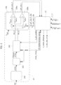
- an electrical power generation system in a vehicle V such as a motor-car may include an alternator A (with stator windings SW and a rotor coil RC), an electronic voltage regulator AVR, a diode rectifier bridge DB, a battery B and various (electrical) loads EL, with operation of the system co-ordinated by an engine control unit ECU.
- alternator A with stator windings SW and a rotor coil RC
- AVR electronic voltage regulator
- DB diode rectifier bridge DB
- battery B and various (electrical) loads EL
- Meaningful inputs for this FSM regulation state can be provided via a protocol from the external control unit ECU and an internal rotation speed signal (coming, for instance, from the three-phase stator system of the alternator A).
- the regulator AVR can be driven to a low-current consumption stand-by state. In that state, the regulator AVR essentially monitors the available sources to detect possible wake-up events (i.e. ECU-driven protocols, key/ignition turn-on engagement, phase signal voltages).
- possible wake-up events i.e. ECU-driven protocols, key/ignition turn-on engagement, phase signal voltages.
- Self-start may play a significant role in facilitating quitting the stand-by state is desired and so-called defined AVR primary wake-up sources (ECU-driven protocols and key/ignition turn-on engagements may be exemplary of these) are not available due to an external system fault (i.e. a fault that occurs outside the alternator assembly at system connector level).
- AVR primary wake-up sources ECU-driven protocols and key/ignition turn-on engagements may be exemplary of these
- exiting the stand-by state may be facilitated thanks to the residual magnetism of the rotor coil RC.
- a rotation speed signal as conventionally fed into an alternator voltage regulator may not fully exploit the voltages from the three-phase stator system SW of the alternator A insofar as only one or two voltages are generally exploited.
- a two-phase configuration may provide a flexible interface for implementing both efficient rectifier bridge diagnostics (when the capability is desired for the regulator to detect the possible presence of one or more diodes in open/short conditions) as well as a robust phase interface based on a differential signal.
- the "phase interface” can be rendered largely insensitive to salt and moisture attacks. Additionally, even appreciable leakage currents from the diode bridge rectifier (i.e. units or tenths of mA) are not in a position to put at risk the residual AC phase voltage, which facilitates reliable amplitude and frequency detection even in hostile environments.
- the former category (synchronous) is mainly characterized by a stand-by current magnitude that may not comply with a low-current specification in stand-by state, for instance due to a clock oscillator kept permanently active.
- the latter category (asynchronous) may give rise to device area issues, for instance due to the usage of a large-area low-frequency RC analog filter.
- One or more embodiments may provide a voltage phase wake-up interface for a voltage regulator such as an alternator voltage regulator AVR as discussed previously based on a single phase signal picked-up from a three-phase stator system SW and capable of providing adequate detection of residual magnetism from the alternator A even in the presence of significant leakage currents from the diode bridge DB and/or a moisture attack: as noted, both of these may result in a large DC component superposed onto the AC input signal to be detected.
- a voltage regulator such as an alternator voltage regulator AVR as discussed previously based on a single phase signal picked-up from a three-phase stator system SW and capable of providing adequate detection of residual magnetism from the alternator A even in the presence of significant leakage currents from the diode bridge DB and/or a moisture attack: as noted, both of these may result in a large DC component superposed onto the AC input signal to be detected.
- One or more embodiments as exemplified herein may comprise an analog circuit block and a digital (numerical) circuit block. These will be referred to in the foregoing as a phase wake-up analog detector circuit block 10 and phase wake-up digital stage or circuit block 12, respectively.
- a wake-up analog detector circuit block 10 as exemplified herein may interface directly with a one-phase voltage signal PH from a three-phase stator SW in an alternator (see, for instance A in Figure 13A ).
- a phase signal can be applied to a corresponding input terminal PH to a voltage regulator (AVR, in the examples presented herein), W or V being other designations currently adopted in the literature for that input in conventional regulators.
- AVR voltage regulator
- the wake-up analog detector circuit block 10 is in charge of capturing a (residual) magnetism amplitude voltage and comparing it against a target threshold voltage.
- the wake-up digital stage or circuit block 12 is in charge of applying digital filter processing as desired (spike rejection filter time, for instance) and executing a control algorithm.
- the wake-up digital stage or circuit block 12 may use a low-frequency, low-current stand-by oscillator 14.
- the stand-by oscillator 14 can be enabled (directly) by the wakeup digital stage 12 as desired.
- the wake-up analog detector circuit block 10 may not use the clock signal from the oscillator 14 in order to evaluate signal amplitude. This facilitates achieving a lower stand-by current consumption in the regulator AVR.
- Figure 1 is an exemplary representation a phase wake-up circuit represented embedded in a AVR stand-by supply domain of the regulator AVR, namely between a stand-by supply voltage at a supply node SBS and a stand-by ground node SBGND.
- phase signal PH may include:
- the outputs from the digital stage 120 may have associated additional signals (e.g., s_wake_phase) as discussed, e.g., in connection with Figure 6 .
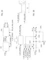
- Figure 2 exemplifies certain possible architecture details of the phase wake-up analog detector circuit block 10.
- the circuit block 10 may comprise:
- the comparator 106 as exemplified herein may use a stable reference voltage VREF (generated in a manner known to those of skill in the art).
- the phase wake-up digital stage or circuit block 12 may facilitate adequate spike rejection times TP SR to filter out undesired spurious glitches affecting window comparator outputs. Also, it may embed a control procedure implemented through a certain number #nds of other I/O digital signals. Some I/O analog signals #nas can be involved as well. In fact, case by case, the cardinality #nds, #nas may depend on the physical implementation for PH_F/PH_S pair signal generator.
- the comparator circuit 106 as exemplified herein includes two comparator stages 106a, 106b providing to the digital stage or circuit block 12 "high” and “low” output signals, namely i_ph_out_h and i_ph_out_l. As exemplified herein, these two signals result from comparing the PH_F signal (which is applied to the non-inverting input of the comparator stage 106a and to the inverting input of the comparator stage 106b) with respective thresholds V REFH (applied to the inverting input of the comparator stage 106a) and V REFL (applied to the non-inverting input of the comparator stage 106b).
- the thresholds V REFH and V REFL are derived from the signal PH_S by applying thereto the offset voltages V OS,H and V OS,L discussed previously.
- the comparator circuit 106 as exemplified herein can be regarded as an "unstructured" window comparator, where - instead of being fused to a single output that goes, e.g., to "1" (only) when the input signal exits the comparator window - the output signals i_ph_out_h and i_ph_out_l are kept separated and used to recognize an increase/decrease in the input signal (here, PH_F).
- a goal pursued in one or more embodiments is to facilitate rejecting DC components of the PH_F signal which might - undesirably - lead to a wake-up event being erroneously declared.
- An increase of the PH_F signal (only) deriving from leakage current in the diodes in the bridge DB of Figure 13A may be exemplary of such DC components.
- Figure 10 is exemplary of a possible case where:
- One or more embodiments may benefit from the "follower" signal PH_S (obtained, e.g. as discussed in the following) in operating the window comparator 106 with non-fixed, time-variable thresholds depending on PH_S (for instance, thresholds that are dynamically set around PH_S), as discussed in the following.
- this may facilitate recognizing a certain (e.g. peak-to-peak) variation in PH_F corresponding to a true AC signal, even in the presence of a (slowly varying) DC component in PH_F.
- a certain (e.g. peak-to-peak) variation in PH_F corresponding to a true AC signal, even in the presence of a (slowly varying) DC component in PH_F.
- one or more embodiments may take advantage from the approaches adopted for generating the signal PH_S.
- Figures 3A - 3B are exemplary of a first possible, non-mandatory implementation of the PH_S/PH_F pair signal generator of the block 104 illustrated in conjunction with the preceding block 102 of Figure 2 .
- the PH_S/PH_F pair generator 104 may comprise a sampling capacitor 1041 with a capacity Cs and two switches 1042, 1043 (two electronic switches such as MOSFET transistors, for instance) to provide sample-and-hold (S & H) circuitry. For instance, after enabling the analog detector 10, if o_ph_sample_n is asserted at a certain level (low, for instance), then both switches 1042 and 1043 are closed.
- the signal PH_F is assumed to correspond to PH (the filtered value A*PH, for instance) while the "follower" signal PH_S is assumed to correspond to a sampled version of A*PH, for instance to A*PH sampled via a sample-and-hold (S & H) action with a period Ts (see the graph on the righthand side of Figure 3B ).
- the switch 1043 is arranged across a resistor 1044 which, together with a capacitor 1045 (with a capacity Cf lower than Cs, for instance) provides an EMC Rf-Cf analog filter.
- the switch 1043 has the capability of reducing the signal source resistance (that is, the resistance of the voltage source charging the sampling capacitor 1041) by "removing", that is, short-circuiting - the resistor 1044 whose resistance is in the range of hundreds of kOhm, when an updated voltage sample is desired to be obtained.
- a source resistance reduction from A*(1-A)*R+Rf down to roughly A*(1-A)*R speeds the charging process of the capacitor 1041.
- Figures 4A - 4B and 5 are exemplary of another possible, non-mandatory implementation of the PH_S/PH_F pair signal generator of the block 104 illustrated in conjunction with the preceding block 102 of Figure 2 .
- FIG. 4A The exemplary implementation of Figures 4A and 4B involves a digital-to-analog (D2A) data converter 1046 operating, for instance, over N-bits embedded in a closed loop configuration.
- D2A digital-to-analog
- o_count ⁇ N-1,0>
- VREF stable reference voltage
- the signal PH_F is again assumed to correspond to the filtered value A*PH, while the "follower" signal PH_S is now assumed to comprise a replica A*PH obtained by a tracking action.
- a switch across the resistor 1044 is no longer used, this being also the case for a switch to force a short circuit between the PH_F and PH_S domains: in the exemplary implementation presented in Figures 4A and 4B this switch can be dispensed with because by enabling PH_S tracking with respect to PH_F, as discussed in the following, a detection disable can be obtained in the phase wake-up digital stage 12 so that a o_ph_enable signal is no longer fed into the phase wake-up analog detector 10.
- the tracked A*PH signal can be obtained through a closed-loop architecture of a mixed type (that is, including both analog and digital sub-stages), that implements as a whole a tracking-mode analog-to-digital (A2D) data converter.
- A2D analog-to-digital
- Such a tracking-mode analog-to-digital data converter may embed an N-bit Up/Down (U/D) counter, which may be arranged in the phase wake-up digital stage 12 and is not explicitly visible in Figures 4A and 4B .
- operation of one or more embodiments as exemplified herein may involve a number of main sub-tasks within a procedure.
- a procedure can be implemented by those of skill in the art as a numerical algorithm running in the phase wake-up digital stage 12, which, in one or more embodiments, may be charged with the task of implementing the procedures exemplified in Figures 6 to 9 .
- sub-tasks may involve:
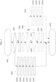
- FIG. 6 to 9 reproduce various flow charts exemplary of possible operation of embodiments.
- Figure 10 is an exemplary representation of a possible time behavior (plotted against a common abscissa time scale t and with arbitrary ordinate scale V) of various (voltage) signals in the exemplary case the signal PH_S is generated via a sample & hold circuitry as exemplified in Figures 3A and 3B , namely:
- Action at 3014 will generate - without the help of the oscillator 14 - the sampling (time) window Ts and lead to the updating of the voltage on the capacitor 1041 in Figure 3B : in fact the sample update.
- the sampling window ends and V(PH_S) assumes a new voltage value integrated and stored, equal to the value assumed by PH_F at the (earlier) switching moment of i_ph_out_h.
- the thresholds V REFH and V REFL which are "constructed" starting from PH_S correspondingly move (upwards, in the exemplary case considered) and the process is completed at 4022, with no changes, i.a. in the o_wake_phase signal intended to prompt a wake-up event (as a result of switching, e.g. to "1").
- V(PH_F) discussed so far in connection with Figure 10 may be of the kind associated with the presence of a (slowly varying) DC component in the signal PH_F, which is thus rejected so that an undesired wake-up event may be avoided.
- V REFH Due to removal of the offset V OS,H at 4012, V REFH will "lie” on the signal V(PH_S) for PH_S.
- V(PH_S) V(PH_F) arranged between V(PH_S) - V OS,L and V(PH_S) + V OS,H .
- Figure 11 is an instrumental reproduction of a possible time behavior, again plotted against a common abscissa time scale t and with arbitrary ordinate scale (voltage V) of time behaviors preceding and around a wake-up-by-phase being recognized as valid at VWU for the following signals (from top to bottom):
- Figure 12 is an exemplary representation of a possible time behavior, plotted against a common abscissa time scale t and with arbitrary ordinate scale (voltage V) of various (voltage) signals in the exemplary case the signal PH_S is generated via a digital-to-analog tracking arrangement as exemplified in Figures 4A, 4B and 5 , namely:
- a track update action replaces the sample update action discussed throughout Figures 6 to 11 .
- such a sample update action may not require activating the oscillator 14, while a track update action as exemplified may involve activation of such an oscillator.
- the wake-up detection circuit may be brought to a permanent sensing mode of the PH_F signal (see, for instance, the active portion VI) on the right hand side of Figure 10 ).
- the wake-up detection circuit when the wake-up detection task has been completed (with a "true" wake-up event identified) the wake-up detection circuit may be kept in a permanent tracking mode of the PH_F signal, with the oscillator 14 possibly on (activated).
- the additional consumption contribution from the oscillator will be generally acceptable insofar as the device will expectedly have a consumption (well) beyond the stand- by current.
- the oscillator may be otherwise kept de-activated (off) in stand-by (portion I in Figure 12 ) to avoid increasing consumption. As noted, the oscillator may be otherwise be activated (turned on) to implement the track update action (portion II in Figure 12 ).
- a method as exemplified herein may comprise:
- updating the comparator window of the window comparator as a function of the replica signal for instance by moving the window upwards as PH_F - and thus PH_S - increase and moving the window downwards as PH_F - and thus PH_S - decrease
- the replica signal PH_S being a slowed-down replica of PH_F (e.g.
- the upper and lower thresholds V REPH and V REFL thresholds of the window comparator will be unable to follow "fast" variations (upwards and downwards) in the PH_F signal corresponding to to a valid wake-up-by-phase event to be recognized.
- the "follower" signal PH_S is designated a slowed-down (or slow-motion) replica of PH_F insofar as PH_S is a replica of PH_F which appears to be moving more slowly (that is, in a retarded or delayed manner) with respect to PH_F.
- a method as exemplified herein may comprise generating the slowed-down replica signal (for instance, PH_S) by digital-to-analog tracking (see, for instance, 1044, 1045, 1046, 1046a in Figures 4A, 4B and 5 ) the signal sensed (A*PH).
- PH_S slowed-down replica signal
- digital-to-analog tracking see, for instance, 1044, 1045, 1046, 1046a in Figures 4A, 4B and 5 .
- a method as exemplified herein may comprise generating (for instance, at 104) the replica signal from an amplitude divided (for instance, at 100) and/or low-pass filtered (for instance, at 102) version (see, for instance A*PH) of the phase signal (PH).
- a circuit as exemplified herein may comprise:
- a circuit as exemplified herein may comprise sampling circuitry activatable to sample the signal sensed (for instance, A*PH) and generate therefrom the slowed-down replica signal.
- a circuit as exemplified herein may comprise digital-to-analog tracking circuitry comprising a time-clocked (for instance, i_sby_ck) up-down counter (for instance, 1046a) configured to track the signal sensed (for instance, A*PH) and generate therefrom the slowed-down replica signal.
- a time-clocked (for instance, i_sby_ck) up-down counter for instance, 1046a
- the input circuitry may comprises an amplitude divider (100) and/or a low-pass filter (102) arranged between the input node (PH) the signal generator circuit block (104).
- an oscillator circuit for instance 14 may be provided selectively activatable (for instance, at 4000a or 4000b) to evaluate the time duration of said window exit signals indicating the signal sensed exiting the comparator window of the window comparator.
- the window comparator may comprise offset voltage control inputs configured to receive offset voltage control signals (for instance, o_ph_vos_h_dis, o_ph_vos_l_dis), wherein the upper and lower thresholds of the comparator window of the window comparator are adjustable as a function of said offset voltage control signals and a threshold value (for instance, VP StartsTh ) for magnetization of said winding in a dynamoelectric machine.
- offset voltage control signals for instance, o_ph_vos_h_dis, o_ph_vos_l_dis
- a device as exemplified herein may comprise:
- An electrical energy generation system as exemplified herein may comprise:
Landscapes
- Engineering & Computer Science (AREA)
- General Physics & Mathematics (AREA)
- Physics & Mathematics (AREA)
- Power Engineering (AREA)
- Chemical & Material Sciences (AREA)
- Combustion & Propulsion (AREA)
- Control Of Eletrric Generators (AREA)
- Life Sciences & Earth Sciences (AREA)
- Sustainable Energy (AREA)
- Transportation (AREA)
- Mechanical Engineering (AREA)
- Sustainable Development (AREA)
- Selective Calling Equipment (AREA)
- Radar Systems Or Details Thereof (AREA)
- Communication Control (AREA)
Claims (13)
- Verfahren, umfassend:- Erfassen (100, 102, 104) eines Signals (PH, A*PH, PH_F), das auf die Magnetisierung einer Wicklung (SW) in einer dynamoelektrischen Maschine (A) hinweist,- Anlegen des erfassten Signals (PH_F) an einen Fenstervergleicher (106), der ein Vergleicherfenster zwischen oberen (V REPH) und unteren (V REFL) Schwellenwerten aufweist, und Erzeugen von Fensteraustrittssignalen (i_ph_out_h, i_ph_out_l), die auf das erfasste Signal (PH_F) hinweisen, das aus dem Vergleicherfenster (V REPH, V REFL) des Fenstervergleichers (106) austreten,dadurch gekennzeichnet, dass das Verfahren umfasst:- Erzeugen (104) eines verlangsamten Replikatsignals (PH_S) des erfassten Signals (PH_F),- Aktualisieren des Vergleicherfensters (VREPH, VREFL) des Fenstervergleichers (106) in Abhängigkeit von dem Replikatsignal (PH_S), und- Ausgeben eines Wecksignals (o_wake_phase) an eine Steuervorrichtung (AVR) der dynamoelektrischen Maschine (A) als Ergebnis von einem der Fensteraustrittssignale (i_ph_out_h, i_ph_out_l), das darauf hinweist (4010, 4014), dass das erfasste Signal (PH_F) das Vergleicherfenster (VREPH, VREFL) des Fenstervergleichers (106) für eine Zeitdauer über einer Dauerschwelle (TPSR) verlässt,wobei das Wecksignal (o_wake_phase) ein Signal umfasst, das dazu bestimmt ist, ein Weckereignis der Steuereinrichtung (AVR) aus einem Standby-Zustand zu veranlassen, wobei das Signal durch Erfüllen von beiden Amplituden- und Zeitkriterien als gültig (VWU) gegenüber falschen Signalen erkannt wird.
- Verfahren nach Anspruch 1, umfassend das Erzeugen des verlangsamten Replikatsignals (PH_S) durch Abtastung (1041 bis 1045) zu diskreten Zeiten (Ts, o_ph_sample_n, o_ph_enable) des erfassten Signals (A*PH).
- Verfahren nach Anspruch 1, umfassend das Erzeugen des verlangsamten Replikatsignals (PH_S) durch Digital-zu-Analog-Verfolgung (1044, 1045, 1046, 1046a) des erfassten Signals (A*PH).
- Verfahren nach einem der vorstehenden Ansprüche, umfassend das Erzeugen (104) des Replikatsignals (PH_S) aus einer amplitudengeteilten (100) und/oder tiefpassgefilterten (102) Version (A*PH) des Signals (PH).
- Schaltung (10, 12), umfassend:- Eingangsschaltkreis (100, 102, 104), der einen Eingangsknoten (PH) aufweist, der konfiguriert ist, um mit einer Wicklung (SW) in einer dynamoelektrischen Maschine (A) gekoppelt zu sein, wobei der Eingangsschaltkreis (100, 102) konfiguriert ist, um ein Signal (PH_F) zu erfassen, das auf eine Magnetisierung der Wicklung (SW) in einer dynamoelektrischen Maschine (A) hinweist,- einen Fenstervergleicher (106), der empfindlich für das erfasste Signal (PH_F) ist, wobei der Vergleicher (106) ein Vergleicherfenster zwischen den oberen (VREPH ) und unteren (VREFL) Schwellenwerten aufweist und konfiguriert ist, um Fensteraustrittssignale (i_ph_out_h, i_ph_out_l) zu erzeugen, die auf das erfasste Signal (PH_F) hinweisen, das aus dem Vergleicherfenster (VREPH, VREFL) des Fenstervergleichers (106) austritt, dadurch gekennzeichnet, dass: das Vergleicherfenster (VREPH, VREFL) in Abhängigkeit von einem Aktualisierungssignal (PH_S) anpassbar ist, und dadurch, dass die Schaltung weiter umfasst:- einen Signalerzeuger-Schaltungsblock (104), der konfiguriert ist, um ein verlangsamtes Replikatsignal (PH_S) des erfassten Signals (PH_F) zu erzeugen, wobei der Signalerzeuger-Schaltungsblock (104) mit dem Fenstervergleicher (106) gekoppelt ist und konfiguriert ist, um das Vergleicherfenster (VREPH, VREFL) des Fenstervergleichers (106) in Abhängigkeit vom Replikatsignals (PH_S) zu aktualisieren, und- Verarbeitungsschaltkreis (12), der empfindlich für die Fensteraustrittssignale (i_ph_out_h, i_ph_out_l) des Fenstervergleichers (106) ist, wobei der Verarbeitungsschaltkreis (12) konfiguriert ist, um ein auf eine Steuervorrichtung (AVR) der dynamoelektrischen Maschine (A) anwendbares Wecksignal (o_wake_phase) als Ergebnis von einem der Fensteraustrittssignale (i_ph_out_h, i_ph_out_1) auszugeben, das darauf hinweist (4010, 4014), dass das erfasste Signal (PH_F) das Vegleicherfenster (VREPH, VREFL) des Fenstervergleichers (106) für eine Zeitdauer über einer Dauerschwelle (TPSR) verlässt,wobei das Wecksignal (o_wake_phase) ein Signal umfasst, das dazu bestimmt ist, ein Weckereignis der Steuereinrichtung (AVR) aus einem Standby-Zustand zu veranlassen, wobei das Signal durch Erfüllen von beiden Amplituden- und Zeitkriterien als gültig (VWU) gegenüber falschen Signalen erkannt wird.
- Schaltung (10, 12) nach Anspruch 5, umfassend eine Abtastschaltung (1041 bis 1045), die zu diskreten Zeiten (Ts, o_ph_sample_n, o_ph_enable) aktivierbar ist, um das erfasste Signal (A*PH) abzutasten und daraus das verlangsamte Replikatsignal (PH_S) zu erzeugen.
- Schaltung (10, 12) nach Anspruch 5, umfassend einen Digital-zu-Analog-Verfolgungsschaltkreis (1044, 1045, 1046, 1046a), der einen zeitlich getakteten (i_sby_ck) Vorwärts-Rückwärts-Zähler (1046a) umfasst, der konfiguriert ist, um das erfasste Signal (A*PH) zu verfolgen und daraus das verlangsamte Replikatsignal (PH_S) zu erzeugen.
- Schaltung (10, 12) nach einem der Ansprüche 5 bis 7, wobei der Eingangsschaltkreis (100, 102) einen Amplitudenteiler (100) und/oder einen Tiefpassfilter (102) umfasst, der zwischen dem Eingangsknoten (PH) und dem Signalerzeuger-Schaltungsblock (104) angeordnet ist.
- Schaltung (10, 12) nach einem der Ansprüche 5 bis 8, wobei eine selektiv aktivierbare (4000a, 4000b) Oszillatorschaltung (14) bereitgestellt ist, um die Zeitdauer der Fensteraustrittssignale (i_ph_out_h, i_ph_out_l) auszuwerten, die auf das erfasste Signal (PH_F) hinweisen (4010, 4014), das aus dem Vergleicherfenster (VREPH, VREFL) des Fenstervergleichers (106) austritt.
- Schaltung (10, 12) nach einem der Ansprüche 5 bis 9, wobei der Fenstervergleicher (106) Offset-Spannungssteuereingänge umfasst, die konfiguriert sind, um Offset-Spannungssteuersignale (o_ph_vos_h_dis, o _ph_vos_l_dis) zu empfangen, wobei die oberen (VREPH) und unteren (VREFL) Schwellenwerte des Vergleicherfensters des Fenstervergleichers (106) in Abhängigkeit von den Offset-Spannungssteuersignalen (o_ph_vos_h_dis, o_ph_vos_1_dis) und einem Schwellenwert (VPstartetTh) zur Magnetisierung der Wicklung (SW) in einer dynamoelektrischen Maschine (A) anpassbar sind.
- Vorrichtung, umfassend:- eine dynamoelektrische Maschine (A), die eine Wicklung (SW) beinhaltet, die Magnetisierungsverhalten zeigen kann,- eine Schaltung (10, 12) nach einem der Ansprüche 5 bis 10, bei welcher der Eingangsknoten (PH) mit der Wicklung (SW) gekoppelt ist.
- Vorrichtung nach Anspruch 11, wobei- die dynamoelektrische Maschine (A) eine Lichtmaschine (A, DB) umfasst, die einen Stator-Wicklungssatz (SW) und eine Rotorspule (RC) aufweist,- ein Lichtmaschinenspannungsregler (AVR) mit der Rotorspule (RC) der Lichtmaschine (A) gekoppelt bereitgestellt ist, um eine Spannungsregelung an der Rotorspule (RC) der Lichtmaschine (A, DB) bereitzustellen.- die Schaltung (10, 12) den Eingangsknoten (PH), der mit einer Statorwicklung in dem Stator-Wicklungssatz (SW) der Lichtmaschine (A, DB) gekoppelt ist, aufweist, um ein Signal (PH) an der Statorwicklung (SW) zu erfassen, und konfiguriert ist, um das Wecksignal (o_wake_phase) in Richtung des Lichtmaschinenspannungsreglers (AVR) auszugeben.
- Elektrisches Energieerzeugungssystem, umfassend:- mindestens eine elektrische Last (EL, B),- eine Vorrichtung (A, DB, AVR) nach Anspruch 12, die mit der mindestens einen elektrischen Last (EL, B) gekoppelt ist, um ihr elektrische Energie zuzuführen.
Applications Claiming Priority (1)
| Application Number | Priority Date | Filing Date | Title |
|---|---|---|---|
| IT102019000002959A IT201900002959A1 (it) | 2019-02-28 | 2019-02-28 | Procedimento per la rilevazione di segnali, circuito, dispositivo e sistema corrispondenti |
Publications (2)
| Publication Number | Publication Date |
|---|---|
| EP3702795A1 EP3702795A1 (de) | 2020-09-02 |
| EP3702795B1 true EP3702795B1 (de) | 2025-04-02 |
Family
ID=66589811
Family Applications (1)
| Application Number | Title | Priority Date | Filing Date |
|---|---|---|---|
| EP20158726.8A Active EP3702795B1 (de) | 2019-02-28 | 2020-02-21 | Signaldetektionsverfahren, entsprechende schaltung, vorrichtung und system |
Country Status (4)
| Country | Link |
|---|---|
| US (1) | US11418139B2 (de) |
| EP (1) | EP3702795B1 (de) |
| CN (2) | CN212343683U (de) |
| IT (1) | IT201900002959A1 (de) |
Families Citing this family (3)
| Publication number | Priority date | Publication date | Assignee | Title |
|---|---|---|---|---|
| IT201900002959A1 (it) * | 2019-02-28 | 2020-08-28 | St Microelectronics Srl | Procedimento per la rilevazione di segnali, circuito, dispositivo e sistema corrispondenti |
| CN114624626B (zh) * | 2020-12-10 | 2025-10-10 | 意法半导体股份有限公司 | 过电流检测电路、对应的系统和方法 |
| CN114675734B (zh) * | 2020-12-25 | 2025-04-08 | 瑞昱半导体股份有限公司 | 具有功率管理机制的电源供应系统及方法 |
Family Cites Families (22)
| Publication number | Priority date | Publication date | Assignee | Title |
|---|---|---|---|---|
| US3533090A (en) * | 1967-12-28 | 1970-10-06 | Foxboro Co | Magnetic analog memory |
| JPS5537881A (en) * | 1978-09-08 | 1980-03-17 | Nippon Denso Co | Automotive generator voltage controller |
| US4314193A (en) * | 1980-05-22 | 1982-02-02 | Motorola, Inc. | Field coil fault detector for automotive alternator battery charging systems |
| DE69310818T2 (de) | 1992-06-25 | 1997-11-27 | Motorola Inc | Wechselstromgeneratorspannungsregler mit Umdrehungsfeststeller und System zum Laden einer Batterie durch diesen Wechselstromgenerator |
| US5448154A (en) * | 1992-07-03 | 1995-09-05 | Hitachi, Ltd. | Control device for battery charging AC generator used in motor vehicle |
| JPH06335298A (ja) * | 1993-03-23 | 1994-12-02 | Mitsubishi Electric Corp | 車両用交流発電機の出力制御方法及び出力制御装置 |
| DE19732961A1 (de) * | 1997-07-31 | 1999-02-04 | Bosch Gmbh Robert | Regler mit Phasenspannungsauswertung für einen Drehstromgenerator |
| FR2810813B1 (fr) * | 2000-06-26 | 2003-10-31 | Denso Corp | Regulateur de tension d'un generateur a courant alternatif pour vehicule |
| JP4186432B2 (ja) * | 2000-08-08 | 2008-11-26 | 株式会社デンソー | 車両用交流発電機の電圧制御装置 |
| US6555993B2 (en) * | 2000-09-28 | 2003-04-29 | Denso Corporation | Voltage regulating system of a vehicle AC generator for charging a battery |
| US6534990B2 (en) * | 2001-07-18 | 2003-03-18 | Delphi Technologies, Inc. | Voltage regulator wake up control using frequency detection |
| GB0523087D0 (en) * | 2005-11-11 | 2005-12-21 | Alstom Power Conversion Ltd | Power converters |
| US8102133B2 (en) * | 2008-07-09 | 2012-01-24 | System General Corporation | Control circuit for BLDC motors |
| US7638966B1 (en) * | 2008-09-03 | 2009-12-29 | Alexander Pummer | Voltage control and power factor correction in AC induction motors |
| CN102195492B (zh) * | 2011-05-24 | 2014-04-16 | 成都芯源系统有限公司 | 同步整流开关电源及其控制电路和控制方法 |
| US9774265B2 (en) * | 2014-03-31 | 2017-09-26 | Stmicroelectronics S.R.L. | Wake up management circuit for a power switching converter |
| FR3022416B1 (fr) * | 2014-06-11 | 2017-08-25 | Valeo Equip Electr Moteur | Boucle de regulation d'un dispositif regulateur numerique de machine electrique tournante a excitation de vehicule automobile |
| US9948188B2 (en) * | 2014-11-04 | 2018-04-17 | Stmicroelectronics S.R.L. | Control device for a quasi-resonant switching converter, and corresponding control method |
| US10094888B2 (en) * | 2014-11-20 | 2018-10-09 | Apple Inc. | Low-power magnetometer assemblies with high offset stability |
| ITUB20150319A1 (it) * | 2015-05-13 | 2016-11-13 | St Microelectronics Srl | Convertitore di corrente con controllo della corrente sul lato dell'avvolgimento primario e compensazione del ritardo di propagazione |
| IT201700022236A1 (it) * | 2017-02-28 | 2018-08-28 | St Microelectronics Srl | Circuito di controllo, alimentatore, apparecchiatura e procedimento corrispondenti |
| IT201900002959A1 (it) * | 2019-02-28 | 2020-08-28 | St Microelectronics Srl | Procedimento per la rilevazione di segnali, circuito, dispositivo e sistema corrispondenti |
-
2019
- 2019-02-28 IT IT102019000002959A patent/IT201900002959A1/it unknown
-
2020
- 2020-02-19 US US16/794,838 patent/US11418139B2/en active Active
- 2020-02-21 EP EP20158726.8A patent/EP3702795B1/de active Active
- 2020-02-27 CN CN202020219572.XU patent/CN212343683U/zh not_active Withdrawn - After Issue
- 2020-02-27 CN CN202010124253.5A patent/CN111624481B/zh active Active
Also Published As
| Publication number | Publication date |
|---|---|
| EP3702795A1 (de) | 2020-09-02 |
| CN111624481B (zh) | 2023-02-03 |
| US20200280274A1 (en) | 2020-09-03 |
| US11418139B2 (en) | 2022-08-16 |
| IT201900002959A1 (it) | 2020-08-28 |
| CN111624481A (zh) | 2020-09-04 |
| CN212343683U (zh) | 2021-01-12 |
Similar Documents
| Publication | Publication Date | Title |
|---|---|---|
| EP3702795B1 (de) | Signaldetektionsverfahren, entsprechende schaltung, vorrichtung und system | |
| CN104656000B (zh) | 检测开关结构中的短路的器件和方法 | |
| JP4295620B2 (ja) | ステッパモータ制御装置 | |
| JP2807579B2 (ja) | 少なくとも2つの異なる交流電源電圧範囲で機能し得る整流器 | |
| JP5079055B2 (ja) | 電力変換装置 | |
| JPH0731078A (ja) | 相巻線検出器および交流発電機充電システム | |
| US6433519B2 (en) | Voltage control unit for vehicular AC generator | |
| TW201206050A (en) | Motor driving circuit | |
| US8461977B2 (en) | Driving circuit for an electric load and electric system comprising the circuit | |
| US11397201B2 (en) | Circuit assembly and method for monitoring sinusoidal alternating voltage signals | |
| US6534990B2 (en) | Voltage regulator wake up control using frequency detection | |
| US20170201091A1 (en) | Power node communication for device detection and control | |
| JP3988292B2 (ja) | 車両用発電制御装置 | |
| JP4193348B2 (ja) | 車両用発電制御装置 | |
| JP4006941B2 (ja) | 車両用発電制御装置 | |
| JP4192427B2 (ja) | 車両用発電制御装置 | |
| JP2000032773A (ja) | インバータ装置 | |
| WO2015155823A1 (ja) | 電力変換装置、電力変換制御方法 | |
| JP3425648B2 (ja) | 多相交流発電機の相間の電圧を検出する検出回路 | |
| CN111934646B (zh) | 用于为晶体振荡器中的晶体注入能量的装置和晶体振荡器 | |
| JP3193175B2 (ja) | 電池電圧低下検出回路 | |
| JP2004208462A (ja) | 電源装置 | |
| KR101000957B1 (ko) | 주파수 감지 장치 및 그 방법 | |
| JP2012170174A (ja) | 2次電池保護回路、2次電池を用いる装置及び2次電池保護方法 | |
| JPH11252979A (ja) | 直流電動機用負荷トルク検出回路 |
Legal Events
| Date | Code | Title | Description |
|---|---|---|---|
| PUAI | Public reference made under article 153(3) epc to a published international application that has entered the european phase |
Free format text: ORIGINAL CODE: 0009012 |
|
| STAA | Information on the status of an ep patent application or granted ep patent |
Free format text: STATUS: THE APPLICATION HAS BEEN PUBLISHED |
|
| AK | Designated contracting states |
Kind code of ref document: A1 Designated state(s): AL AT BE BG CH CY CZ DE DK EE ES FI FR GB GR HR HU IE IS IT LI LT LU LV MC MK MT NL NO PL PT RO RS SE SI SK SM TR |
|
| AX | Request for extension of the european patent |
Extension state: BA ME |
|
| STAA | Information on the status of an ep patent application or granted ep patent |
Free format text: STATUS: REQUEST FOR EXAMINATION WAS MADE |
|
| 17P | Request for examination filed |
Effective date: 20201202 |
|
| RBV | Designated contracting states (corrected) |
Designated state(s): AL AT BE BG CH CY CZ DE DK EE ES FI FR GB GR HR HU IE IS IT LI LT LU LV MC MK MT NL NO PL PT RO RS SE SI SK SM TR |
|
| STAA | Information on the status of an ep patent application or granted ep patent |
Free format text: STATUS: EXAMINATION IS IN PROGRESS |
|
| 17Q | First examination report despatched |
Effective date: 20221219 |
|
| GRAP | Despatch of communication of intention to grant a patent |
Free format text: ORIGINAL CODE: EPIDOSNIGR1 |
|
| STAA | Information on the status of an ep patent application or granted ep patent |
Free format text: STATUS: GRANT OF PATENT IS INTENDED |
|
| RIC1 | Information provided on ipc code assigned before grant |
Ipc: H02P 9/48 20060101ALI20241128BHEP Ipc: H02J 7/24 20060101ALI20241128BHEP Ipc: H02P 9/30 20060101ALI20241128BHEP Ipc: H02P 9/08 20060101ALI20241128BHEP Ipc: H02J 7/14 20060101ALI20241128BHEP Ipc: G01R 31/34 20200101AFI20241128BHEP |
|
| INTG | Intention to grant announced |
Effective date: 20241212 |
|
| GRAS | Grant fee paid |
Free format text: ORIGINAL CODE: EPIDOSNIGR3 |
|
| GRAA | (expected) grant |
Free format text: ORIGINAL CODE: 0009210 |
|
| STAA | Information on the status of an ep patent application or granted ep patent |
Free format text: STATUS: THE PATENT HAS BEEN GRANTED |
|
| AK | Designated contracting states |
Kind code of ref document: B1 Designated state(s): AL AT BE BG CH CY CZ DE DK EE ES FI FR GB GR HR HU IE IS IT LI LT LU LV MC MK MT NL NO PL PT RO RS SE SI SK SM TR |
|
| REG | Reference to a national code |
Ref country code: GB Ref legal event code: FG4D |
|
| REG | Reference to a national code |
Ref country code: CH Ref legal event code: EP |
|
| REG | Reference to a national code |
Ref country code: IE Ref legal event code: FG4D |
|
| REG | Reference to a national code |
Ref country code: DE Ref legal event code: R096 Ref document number: 602020048594 Country of ref document: DE |
|
| REG | Reference to a national code |
Ref country code: NL Ref legal event code: MP Effective date: 20250402 |
|
| PG25 | Lapsed in a contracting state [announced via postgrant information from national office to epo] |
Ref country code: NL Free format text: LAPSE BECAUSE OF FAILURE TO SUBMIT A TRANSLATION OF THE DESCRIPTION OR TO PAY THE FEE WITHIN THE PRESCRIBED TIME-LIMIT Effective date: 20250402 |
|
| REG | Reference to a national code |
Ref country code: AT Ref legal event code: MK05 Ref document number: 1781758 Country of ref document: AT Kind code of ref document: T Effective date: 20250402 |
|
| PG25 | Lapsed in a contracting state [announced via postgrant information from national office to epo] |
Ref country code: FI Free format text: LAPSE BECAUSE OF FAILURE TO SUBMIT A TRANSLATION OF THE DESCRIPTION OR TO PAY THE FEE WITHIN THE PRESCRIBED TIME-LIMIT Effective date: 20250402 Ref country code: PT Free format text: LAPSE BECAUSE OF FAILURE TO SUBMIT A TRANSLATION OF THE DESCRIPTION OR TO PAY THE FEE WITHIN THE PRESCRIBED TIME-LIMIT Effective date: 20250804 Ref country code: ES Free format text: LAPSE BECAUSE OF FAILURE TO SUBMIT A TRANSLATION OF THE DESCRIPTION OR TO PAY THE FEE WITHIN THE PRESCRIBED TIME-LIMIT Effective date: 20250402 |
|
| REG | Reference to a national code |
Ref country code: LT Ref legal event code: MG9D |
|
| PG25 | Lapsed in a contracting state [announced via postgrant information from national office to epo] |
Ref country code: NO Free format text: LAPSE BECAUSE OF FAILURE TO SUBMIT A TRANSLATION OF THE DESCRIPTION OR TO PAY THE FEE WITHIN THE PRESCRIBED TIME-LIMIT Effective date: 20250702 Ref country code: GR Free format text: LAPSE BECAUSE OF FAILURE TO SUBMIT A TRANSLATION OF THE DESCRIPTION OR TO PAY THE FEE WITHIN THE PRESCRIBED TIME-LIMIT Effective date: 20250703 |
|
| PG25 | Lapsed in a contracting state [announced via postgrant information from national office to epo] |
Ref country code: PL Free format text: LAPSE BECAUSE OF FAILURE TO SUBMIT A TRANSLATION OF THE DESCRIPTION OR TO PAY THE FEE WITHIN THE PRESCRIBED TIME-LIMIT Effective date: 20250402 |
|
| PG25 | Lapsed in a contracting state [announced via postgrant information from national office to epo] |
Ref country code: BG Free format text: LAPSE BECAUSE OF FAILURE TO SUBMIT A TRANSLATION OF THE DESCRIPTION OR TO PAY THE FEE WITHIN THE PRESCRIBED TIME-LIMIT Effective date: 20250402 |
|
| PG25 | Lapsed in a contracting state [announced via postgrant information from national office to epo] |
Ref country code: HR Free format text: LAPSE BECAUSE OF FAILURE TO SUBMIT A TRANSLATION OF THE DESCRIPTION OR TO PAY THE FEE WITHIN THE PRESCRIBED TIME-LIMIT Effective date: 20250402 |
|
| PG25 | Lapsed in a contracting state [announced via postgrant information from national office to epo] |
Ref country code: AT Free format text: LAPSE BECAUSE OF FAILURE TO SUBMIT A TRANSLATION OF THE DESCRIPTION OR TO PAY THE FEE WITHIN THE PRESCRIBED TIME-LIMIT Effective date: 20250402 |
|
| PG25 | Lapsed in a contracting state [announced via postgrant information from national office to epo] |
Ref country code: RS Free format text: LAPSE BECAUSE OF FAILURE TO SUBMIT A TRANSLATION OF THE DESCRIPTION OR TO PAY THE FEE WITHIN THE PRESCRIBED TIME-LIMIT Effective date: 20250702 |
|
| PG25 | Lapsed in a contracting state [announced via postgrant information from national office to epo] |
Ref country code: IS Free format text: LAPSE BECAUSE OF FAILURE TO SUBMIT A TRANSLATION OF THE DESCRIPTION OR TO PAY THE FEE WITHIN THE PRESCRIBED TIME-LIMIT Effective date: 20250802 |
|
| PG25 | Lapsed in a contracting state [announced via postgrant information from national office to epo] |
Ref country code: LV Free format text: LAPSE BECAUSE OF FAILURE TO SUBMIT A TRANSLATION OF THE DESCRIPTION OR TO PAY THE FEE WITHIN THE PRESCRIBED TIME-LIMIT Effective date: 20250402 |
|
| PG25 | Lapsed in a contracting state [announced via postgrant information from national office to epo] |
Ref country code: DK Free format text: LAPSE BECAUSE OF FAILURE TO SUBMIT A TRANSLATION OF THE DESCRIPTION OR TO PAY THE FEE WITHIN THE PRESCRIBED TIME-LIMIT Effective date: 20250402 Ref country code: SM Free format text: LAPSE BECAUSE OF FAILURE TO SUBMIT A TRANSLATION OF THE DESCRIPTION OR TO PAY THE FEE WITHIN THE PRESCRIBED TIME-LIMIT Effective date: 20250402 |
|
| PG25 | Lapsed in a contracting state [announced via postgrant information from national office to epo] |
Ref country code: CZ Free format text: LAPSE BECAUSE OF FAILURE TO SUBMIT A TRANSLATION OF THE DESCRIPTION OR TO PAY THE FEE WITHIN THE PRESCRIBED TIME-LIMIT Effective date: 20250402 |
|
| PG25 | Lapsed in a contracting state [announced via postgrant information from national office to epo] |
Ref country code: EE Free format text: LAPSE BECAUSE OF FAILURE TO SUBMIT A TRANSLATION OF THE DESCRIPTION OR TO PAY THE FEE WITHIN THE PRESCRIBED TIME-LIMIT Effective date: 20250402 |
|
| PG25 | Lapsed in a contracting state [announced via postgrant information from national office to epo] |
Ref country code: SK Free format text: LAPSE BECAUSE OF FAILURE TO SUBMIT A TRANSLATION OF THE DESCRIPTION OR TO PAY THE FEE WITHIN THE PRESCRIBED TIME-LIMIT Effective date: 20250402 Ref country code: RO Free format text: LAPSE BECAUSE OF FAILURE TO SUBMIT A TRANSLATION OF THE DESCRIPTION OR TO PAY THE FEE WITHIN THE PRESCRIBED TIME-LIMIT Effective date: 20250402 |
|
| PG25 | Lapsed in a contracting state [announced via postgrant information from national office to epo] |
Ref country code: IT Free format text: LAPSE BECAUSE OF FAILURE TO SUBMIT A TRANSLATION OF THE DESCRIPTION OR TO PAY THE FEE WITHIN THE PRESCRIBED TIME-LIMIT Effective date: 20250402 |
|
| PLBE | No opposition filed within time limit |
Free format text: ORIGINAL CODE: 0009261 |
|
| STAA | Information on the status of an ep patent application or granted ep patent |
Free format text: STATUS: NO OPPOSITION FILED WITHIN TIME LIMIT |
|
| REG | Reference to a national code |
Ref country code: CH Ref legal event code: L10 Free format text: ST27 STATUS EVENT CODE: U-0-0-L10-L00 (AS PROVIDED BY THE NATIONAL OFFICE) Effective date: 20260211 |