EP3702722B1 - Dehnungsmesser und sensormodul - Google Patents
Dehnungsmesser und sensormodul Download PDFInfo
- Publication number
- EP3702722B1 EP3702722B1 EP18871642.7A EP18871642A EP3702722B1 EP 3702722 B1 EP3702722 B1 EP 3702722B1 EP 18871642 A EP18871642 A EP 18871642A EP 3702722 B1 EP3702722 B1 EP 3702722B1
- Authority
- EP
- European Patent Office
- Prior art keywords
- resistor
- strain gauge
- functional layer
- layer
- substrate
- Prior art date
- Legal status (The legal status is an assumption and is not a legal conclusion. Google has not performed a legal analysis and makes no representation as to the accuracy of the status listed.)
- Active
Links
Images




Classifications
-
- G—PHYSICS
- G01—MEASURING; TESTING
- G01L—MEASURING FORCE, STRESS, TORQUE, WORK, MECHANICAL POWER, MECHANICAL EFFICIENCY, OR FLUID PRESSURE
- G01L1/00—Measuring force or stress, in general
- G01L1/20—Measuring force or stress, in general by measuring variations in ohmic resistance of solid materials or of electrically-conductive fluids; by making use of electrokinetic cells, i.e. liquid-containing cells wherein an electrical potential is produced or varied upon the application of stress
- G01L1/22—Measuring force or stress, in general by measuring variations in ohmic resistance of solid materials or of electrically-conductive fluids; by making use of electrokinetic cells, i.e. liquid-containing cells wherein an electrical potential is produced or varied upon the application of stress using resistance strain gauges
- G01L1/225—Measuring circuits therefor
-
- G—PHYSICS
- G01—MEASURING; TESTING
- G01B—MEASURING LENGTH, THICKNESS OR SIMILAR LINEAR DIMENSIONS; MEASURING ANGLES; MEASURING AREAS; MEASURING IRREGULARITIES OF SURFACES OR CONTOURS
- G01B7/00—Measuring arrangements characterised by the use of electric or magnetic techniques
- G01B7/16—Measuring arrangements characterised by the use of electric or magnetic techniques for measuring the deformation in a solid, e.g. by resistance strain gauge
- G01B7/18—Measuring arrangements characterised by the use of electric or magnetic techniques for measuring the deformation in a solid, e.g. by resistance strain gauge using change in resistance
- G01B7/20—Measuring arrangements characterised by the use of electric or magnetic techniques for measuring the deformation in a solid, e.g. by resistance strain gauge using change in resistance formed by printed-circuit technique
-
- G—PHYSICS
- G01—MEASURING; TESTING
- G01L—MEASURING FORCE, STRESS, TORQUE, WORK, MECHANICAL POWER, MECHANICAL EFFICIENCY, OR FLUID PRESSURE
- G01L5/00—Apparatus for, or methods of, measuring force, work, mechanical power, or torque, specially adapted for specific purposes
- G01L5/0028—Force sensors associated with force applying means
-
- H—ELECTRICITY
- H01—ELECTRIC ELEMENTS
- H01C—RESISTORS
- H01C7/00—Non-adjustable resistors formed as one or more layers or coatings; Non-adjustable resistors made from powdered conducting material or powdered semi-conducting material with or without insulating material
- H01C7/003—Thick film resistors
-
- H—ELECTRICITY
- H05—ELECTRIC TECHNIQUES NOT OTHERWISE PROVIDED FOR
- H05K—PRINTED CIRCUITS; CASINGS OR CONSTRUCTIONAL DETAILS OF ELECTRIC APPARATUS; MANUFACTURE OF ASSEMBLAGES OF ELECTRICAL COMPONENTS
- H05K1/00—Printed circuits
- H05K1/16—Printed circuits incorporating printed electric components, e.g. printed resistors, capacitors or inductors
- H05K1/167—Printed circuits incorporating printed electric components, e.g. printed resistors, capacitors or inductors incorporating printed resistors
-
- H—ELECTRICITY
- H05—ELECTRIC TECHNIQUES NOT OTHERWISE PROVIDED FOR
- H05K—PRINTED CIRCUITS; CASINGS OR CONSTRUCTIONAL DETAILS OF ELECTRIC APPARATUS; MANUFACTURE OF ASSEMBLAGES OF ELECTRICAL COMPONENTS
- H05K1/00—Printed circuits
- H05K1/02—Details
- H05K1/0277—Bendability or stretchability details
- H05K1/028—Bending or folding regions of flexible printed circuits
-
- H—ELECTRICITY
- H05—ELECTRIC TECHNIQUES NOT OTHERWISE PROVIDED FOR
- H05K—PRINTED CIRCUITS; CASINGS OR CONSTRUCTIONAL DETAILS OF ELECTRIC APPARATUS; MANUFACTURE OF ASSEMBLAGES OF ELECTRICAL COMPONENTS
- H05K1/00—Printed circuits
- H05K1/02—Details
- H05K1/0296—Conductive pattern lay-out details not covered by sub groups H05K1/02 - H05K1/0295
- H05K1/0298—Multilayer circuits
-
- H—ELECTRICITY
- H05—ELECTRIC TECHNIQUES NOT OTHERWISE PROVIDED FOR
- H05K—PRINTED CIRCUITS; CASINGS OR CONSTRUCTIONAL DETAILS OF ELECTRIC APPARATUS; MANUFACTURE OF ASSEMBLAGES OF ELECTRICAL COMPONENTS
- H05K1/00—Printed circuits
- H05K1/02—Details
- H05K1/03—Use of materials for the substrate
- H05K1/0313—Organic insulating material
- H05K1/032—Organic insulating material consisting of one material
-
- H—ELECTRICITY
- H05—ELECTRIC TECHNIQUES NOT OTHERWISE PROVIDED FOR
- H05K—PRINTED CIRCUITS; CASINGS OR CONSTRUCTIONAL DETAILS OF ELECTRIC APPARATUS; MANUFACTURE OF ASSEMBLAGES OF ELECTRICAL COMPONENTS
- H05K1/00—Printed circuits
- H05K1/02—Details
- H05K1/03—Use of materials for the substrate
- H05K1/0393—Flexible materials
-
- H—ELECTRICITY
- H05—ELECTRIC TECHNIQUES NOT OTHERWISE PROVIDED FOR
- H05K—PRINTED CIRCUITS; CASINGS OR CONSTRUCTIONAL DETAILS OF ELECTRIC APPARATUS; MANUFACTURE OF ASSEMBLAGES OF ELECTRICAL COMPONENTS
- H05K2201/00—Indexing scheme relating to printed circuits covered by H05K1/00
- H05K2201/10—Details of components or other objects attached to or integrated in a printed circuit board
- H05K2201/10007—Types of components
- H05K2201/10151—Sensor
Definitions
- the present invention relates to a strain gauge and a sensor module.
- Strain gauges that have been known are attached to an object to be measured so as to detect a strain of the object.
- a strain gauge includes a resistor for detecting a strain, and as materials of the resistor, materials containing, for example, Cr (chromium) and/or Ni (nickel) are used. Also, for example, both ends of the resistor are used as electrodes, and a lead wire or the like for external connection is joined to each electrode by solder, so that a signal can be input and output to and from an electronic component (see, e.g., Patent Document 1) .
- Other examples of strain gauges are disclosed in JP H06 307950 A , JP 2017 101983 A and JP H10 270201 A .
- Patent Document 1 Japanese Unexamined Patent Application Publication No.2016-74934
- the present invention has been made in view of the above point, and has an object to make a strain gauge smaller.
- the present application also discloses a strain gauge including a substrate having flexibility; a resistor formed from a material containing at least one of chromium and nickel, on the substrate; a pair of wiring patterns formed on the substrate and electrically connected to both ends of the resistor; and a pair of electrodes formed on the substrate and electrically connected to the pair of wiring patterns, respectively.
- the wiring patterns include a first layer extending from the resistor, and a second layer having a lower resistance than the first layer and layered on the first layer.
- an electronic component mounting area is demarcated, on which an electronic component electrically connected to the electrodes is mounted.
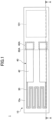
- FIG. 1 is a plan view illustrating a strain gauge according to a first embodiment.
- FIG. 2 is a cross-sectional view illustrating a strain gauge according to the first embodiment, which illustrates a cross section taken along a line AA in FIG. 1 .
- a strain gauge 1 includes a substrate 10, a resistor 30, wiring patterns 40, and electrodes 40A.
- a side of the strain gauge 1 on which the resistor 30 of the substrate 10 is provided is defined as an upper side or one side, and another side on which the resistor 30 is not provided is defined as a lower side or the other side.
- a surface of each part on which the resistor 30 is provided is defined as one surface or upper surface, and another surface on which the resistor 30 is not provided is defined as the other surface or lower surface.
- the strain gauge 1 can be used upside down, or can be arranged at any angle.
- a plan view refers to viewing an object from the normal direction of the upper surface 10a of the substrate 10
- a planar shape refers to a shape of an object viewed from the normal direction of the upper surface 10a of the substrate 10.
- the substrate 10 is a member serving as a base layer for forming the resistor 30 and the like, and has flexibility.
- the thickness of the substrate 10 is not limited in particular and can be selected appropriately depending on the purpose; for example, the thickness can be approximately 5 um to 500 um. Especially, it is favorable that the thickness of the substrate 10 is between 5 um and 200 um from the viewpoint of the transmission of strain from the surface of the strain generator joined to the lower surface of the substrate 10 via an adhesive layer or the like, and the dimensional stability with respect to the environment; and it is more favorable that the thickness is greater than or equal to 10 um from the viewpoint of insulation.
- the substrate 10 can be formed from an insulating resin film, for example, PI (polyimide) resin, epoxy resin, PEEK (polyether ether ketone) resin, PEN (polyethylene naphthalate) resin, PET (polyethylene terephthalate) resin, PPS (polyphenylene sulfide) resin, polyolefin resin, or the like.
- PI polyimide
- epoxy resin epoxy resin
- PEEK polyether ether ketone
- PEN polyethylene naphthalate
- PET polyethylene terephthalate
- PPS polyphenylene sulfide
- the substrate 10 may be formed from, for example, an insulating resin film containing a filler such as silica or alumina.
- an electronic component mounting area 101 is demarcated, on which an electronic component electrically connected to the electrodes 40A is mounted.
- Electronic components that can be mounted on the electronic component mounting area 101 include an active component such as a semiconductor chip and a passive component such as a capacitor.
- a wiring pattern electrically connected to the electronic component may be formed.
- the resistor 30 is a thin film formed on the substrate 10 to have a predetermined pattern, which is a sensing part in which a resistance change is generated in response to a strain.
- the resistor 30 may be formed directly on the upper surface 10a of the substrate 10, or may be formed on the upper surface 10a of the substrate 10 via another layer. Note that in FIG. 1 , the resistor 30 is illustrated in a dot pattern for the sake of convenience.
- the resistor 30 can be formed from, for example, a material containing Cr (chromium), a material containing Ni (nickel), or a material containing both Cr and Ni.
- the resistor 30 can be formed from a material containing at least one of Cr and Ni.
- a Cr composite film may be cited as an example of the material containing Cr.
- the material containing Ni for example, Cu-Ni (copper-nickel) may be cited.
- Ni-Cr nickel-chrome
- the Cr composite film is a film in which Cr, CrN, Cr 2 N, and the like are mixed.
- the Cr composite film may contain unavoidable impurities such as chromium oxide.
- the thickness of the resistor 30 is not limited in particular and can be selected appropriately depending on the purpose; for example, the thickness can be approximately 0.05 ⁇ m to 2 ⁇ m. Especially, it is favorable that the thickness of the resistor 30 is greater than or equal to 0.1 um because the crystallinity of crystals constituting the resistor 30 (e.g., the crystallinity of ⁇ -Cr) improves, and it is further favorable that the thickness is less than or equal to 1 um because cracks in the film and/or the warp from the substrate 10 due to the internal stress of the film constituting the resistor 30 can be reduced.
- the thickness of the resistor 30 is greater than or equal to 0.1 um because the crystallinity of crystals constituting the resistor 30 (e.g., the crystallinity of ⁇ -Cr) improves, and it is further favorable that the thickness is less than or equal to 1 um because cracks in the film and/or the warp from the substrate 10 due to the internal stress of the film constituting the resistor 30 can be reduced.
- the stability of the gauge characteristics can be improved by using ⁇ -Cr (alpha chromium), which is a stable crystal phase, as the main component.
- the gauge factor of the strain gauge 1 can be greater than or equal to 10
- the temperature coefficient of gauge factor TCS and the temperature coefficient of resistance TCR can be fallen within a range of -1000 ppm/°C to +1000 ppm/°C.
- the main component means that a substance accounts for greater than or equal to 50 mass% among all substances constituting the resistor; from the viewpoint of improving the gauge characteristics, it is favorable that the resistor 30 contains ⁇ -Cr by greater than or equal to 80 wt%.
- ⁇ -Cr is Cr having a bcc structure (body-centered cubic lattice structure).
- the wiring patterns 40 are a pair of wiring patterns electrically connected to both ends of the resistor 30.
- the wiring patterns 40 include a first layer 41, and a second layer 42 layered on the first layer 41.
- the first layer 41 extends from both ends of the resistor 30, and is formed in a substantially rectangular shape having a wider width than the resistor 30 in plan view.
- the second layer 42 is layered on the upper surface of the first layer 41.
- the resistor 30 extends, for example, in a zigzag way from one of the wiring patterns 40 and is connected to the other of the wiring patterns 40.
- the wiring pattern 40 is not limited to a linear shape, and may have any pattern. Also, the wiring pattern 40 can have any width and any length.
- Each electrode 40A is electrically connected to a corresponding wiring pattern 40.
- the electrodes 40A are a pair of electrodes for outputting a change in the resistance value of the resistor 30 caused by a strain, and can be electrically connected to an electronic component mounted on the electronic component mounting area 101.
- the electrode 40A may be formed to have a width different from that of the wiring pattern 40.
- the second layer 42 has a lower resistance than the first layer 41.
- the material of the second layer 42 is not limited in particular and may be appropriately selected depending on the purpose as long as the material has a lower resistance than the first layer 41; for example, Cu, a Cu alloy, Ni, or a Ni alloy may be used.
- the thickness of the second layer 42 may be, for example, approximately 0.5 um to 30 um.
- the second layer 42 may be a layered film.
- a layered film Cu/Ni/Au, Cu/NiP/Au, Cu/Pd/Au, Cu/Pt/Au, Ni/Au, NiP/Au, and the like may be listed.
- AA/BB means a layered film in which an AA layer and a BB layer are layered in this order on the upper surface of an underlying layer (the same applies to a case of three layers or more) .
- a Cu alloy may be used instead of Cu
- a Ni alloy may be used instead of Ni.
- the wiring pattern 40 and the electrode 40A may be integrally formed of the same material in the same process.
- the layer configuration of the electrode 40A may be different from the layer configuration of the wiring pattern 40.
- Au or the like may be formed only on the uppermost layer of the electrode 40A to improve the connection reliability.
- external input/output terminals can be provided at any positions on the upper surface 10a of the substrate 10, which can be electrically connected to an electronic component mounted on the electronic component mounting area 101, and allows signals inputting and outputting to and from an external circuit electrically connected to the strain gauge 1.
- a cover layer 60A (a first insulating resin layer) may be provided on the upper surface 10a of the substrate 10, so as to cover the resistor 30 and the wiring patterns 40, and to expose the electrodes 40A and the electronic component mounting area 101.
- the cover layer 60A it is possible to prevent mechanical damage and the like from occurring in the resistor 30 and the wiring patterns 40. Also, by providing the cover layer 60A, it is possible to protect the resistor 30 and the wiring patterns 40 from moisture and the like.
- the cover layer 60A may be provided so as to cover the entire part excluding the electrodes 40A and the electronic component mounting area 101.
- the cover layer 60A can be formed from an insulating resin; for example, PI resin, epoxy resin, PEEK resin, PEN resin, PET resin, PPS resin, composite resin (e.g., silicone resin, polyolefin resin), or the like.
- the cover layer 60A may contain a filler or a pigment.
- the thickness of the cover layer 60A is not limited in particular and can be selected appropriately depending on the purpose; for example, the thickness can be approximately 2 um to 30 um.
- a substrate 10 is prepared, and a planar resistor 30 and a first layer 41 as illustrated in FIG. 1 are formed on the upper surface 10a of the substrate 10.
- the material and thickness of the resistor 30 and the first layer 41 are as described above.
- the resistor 30 and the first layer 41 can be integrally formed of the same material.
- the resistor 30 and the first layer 41 can be formed by, for example, forming a film by a magnetron sputtering method using a material capable of forming the resistor 30 and the first layer 41 as a target, and patterning the film by photolithography.
- the resistor 30 and the first layer 41 may be formed using a reactive sputtering method, an evaporation method, an arc ion plating method, a pulse laser deposition method, or the like instead of the magnetron sputtering method.
- the resistor 30 and the first layer 41 as a film, as an underlayer, it is favorable to form in vacuum a functional layer as a film having a thickness of approximately 1 nm to 100 nm on the upper surface 10a of the substrate 10 by, for example, a conventional sputtering method.
- the functional layer is patterned by photolithography together with the resistor 30 and the first layer 41 into a planar shape as illustrated in FIG. 1 .
- the functional layer refers to a layer having a function of promoting crystal growth of at least the resistor 30 as the upper layer. It is favorable that the functional layer further has a function of preventing oxidation of the resistor 30 due to oxygen and moisture contained in the substrate 10, and a function of improving the adhesion between the substrate 10 and the resistor 30.
- the functional layer may further have other functions.
- the insulating resin film constituting the substrate 10 contains oxygen and moisture, and thereby, especially when the resistor 30 contains Cr, Cr forms a self-oxidized film; therefore, it is effective that the functional layer has a function of preventing oxidation of the resistor 30.
- the material of the functional layer is not limited in particular as long as it has a function of promoting crystal growth of at least the resistor 30 as the upper layer, and can be appropriately selected depending on the purpose; as the material, one or more species of metals selected from among a group consisting of, for example, Cr (chromium), Ti (titanium), V (vanadium), Nb (niobium), Ta (tantalum), Ni (nickel), Y (yttrium), Zr (zirconium), Hf (hafnium), Si (silicon), C (carbon), Zn (zinc), Cu (copper), Bi (bismuth), Fe (iron), Mo (molybdenum), W (tungsten), Ru (ruthenium), Rh (rhodium), Re (rhenium)), Os (osmium), Ir (iridium), Pt (platinum), Pd (palladium), Ag (silver), Au (gold), Co (cobalt), Mn (manganese), and Al (alum
- FeCr, TiAl, FeNi, NiCr, CrCu, and the like may be listed.
- TiN, TaN, Si 3 N 4 , TiO 2 , Ta 2 O 5 , SiO 2 , and the like may be listed.
- the functional layer can be formed by, for example, a conventional sputtering method using a material capable of forming the functional layer as a target, and introducing Ar (argon) gas into the chamber.
- Ar argon
- the functional layer is formed as a film while the upper surface 10a of the substrate 10 is being etched with Ar; therefore, the effect of improving the adhesion can be obtained by minimizing the amount of the functional layer formed as a film.
- the functional layer may be formed by another method.
- a method may be used in which the upper surface 10a of the substrate 10 is activated by plasma treatment using Ar or the like before forming the functional layer so as to obtain an adhesion improving effect, and then, the functional layer is formed in vacuum as a film by a magnetron sputtering method.
- the combination of the material of the functional layer and the material of the resistor 30 and the first layer 41 is not limited in particular and can be appropriately selected depending on the purpose; for example, it is possible to use Ti as the functional layer, and to form a Cr composite film containing ⁇ -Cr (alpha chromium) as the main component, as the resistor 30 and the first layer 41.
- the resistor 30 and the first layer 41 can be formed as a film by a magnetron sputtering method using a material capable of forming a Cr composite film as a target, and introducing Ar gas into the chamber.
- the resistor 30 and the first layer 41 may be formed as a film by a reactive sputtering method using pure Cr as a target, and introducing an appropriate amount of nitrogen gas together with Ar gas into the chamber.
- a growth face of the Cr mixed-phase film is defined and triggered by the functional layer formed of Ti, which enables to form a Cr composite film containing, as the main component, ⁇ -Cr having a stable crystal structure.
- the gauge characteristics are improved by Ti constituting the functional layer diffusing into the Cr composite film.
- the gauge factor of the strain gauge 1 can be greater than or equal to 10
- the temperature coefficient of gauge factor TCS and the temperature coefficient of resistance TCR can be fallen within a range of -1000 ppm/°C to +1000 ppm/°C.
- the Cr composite film may contain Ti or TiN (titanium nitride).
- the functional layer made of Ti has all of the function of promoting the crystal growth of resistor 30; the function of preventing oxidation of the resistor 30 due to oxygen and moisture contained in the substrate 10; and the function of improving the adhesion between the substrate 10 and the resistor 30.
- the functional layer made of Ti has all of the function of promoting the crystal growth of resistor 30; the function of preventing oxidation of the resistor 30 due to oxygen and moisture contained in the substrate 10; and the function of improving the adhesion between the substrate 10 and the resistor 30.
- Ta, Si, Al, or Fe instead of Ti as the functional layer.
- the crystal growth of the resistor 30 can be promoted, and the resistor 30 having a stable crystal phase can be manufactured.
- the stability of the gauge characteristics of the strain gauge 1 can be improved.
- the gauge characteristics of the strain gauge 1 can be improved.
- a second layer 42 is layered on the first layer 41.
- the material and thickness of the second layer 42 are as described above.
- the second layer 42 can be formed by, for example, an electrolytic plating method or an electroless plating method.
- the strain gauge 1 After having the second layer 42 formed, if necessary, by providing a cover layer 60A on the upper surface 10a of the substrate 10, so as to cover the resistor 30 and the wiring patterns 40, and to expose the electrodes 40A and the electronic component mounting area 101, the strain gauge 1 is completed.
- the cover layer 60A can be manufactured, for example, by laminating a thermosetting insulating resin film in a semi-cured state on the upper surface 10a of the substrate 10, so as to cover the resistor 30 and the wiring patterns 40, and to expose the electrodes 40A and the electronic component mounting area 101, and heating the laminated film to be cured.
- the cover layer 60A may also be manufactured by applying a liquid or paste-like thermosetting insulating resin to the upper surface 10a of the substrate 10, so as to cover the resistor 30 and the wiring patterns 40, and to expose the electrodes 40A and the electronic component mounting area 101, and heating the resin to be cured.
- the strain gauge 1 has a cross-sectional shape illustrated in FIG. 3 .
- a layer indicated by a reference numeral 20 is the functional layer.
- the planar shape of the strain gauge 1 in the case of providing the functional layer 20 is the same as that in FIG. 1 .
- the resistor 30, the wiring patterns 40, the electrodes 40A, and the electronic component mounting area 101 are provided on the upper surface 10a of one substrate 10.
- This enables an electronic component mounted on the electronic component mounting area 101 and the electrodes 40A, to be connected within a short distance by metal wires and the like; therefore, the distance from the resistor 30 to the electronic component can be shortened, and the strain gauge 1 can be implemented to have a small size.
- This structure is particularly effective for a small strain gauge in which it is difficult to connect the resistor and the electronic component with each other using lead wires by soldering or the like.
- the noise resistance can be improved.
- the electrodes 40A have a structure in which the second layer 42 is layered on the first layer 41. Therefore, by selecting the material of the second layer 42, it is possible to improve the connection reliability with an electronic component without depending on the material of the first layer 41 which is the same material as the resistor 30.
- a strain gauge In a modified example 1 of the first embodiment, an example of a strain gauge will be described in which electronic components are mounted on an electronic component mounting area. Note that in the modified example 1 of the first embodiment, description of the same components as those already described may be omitted.
- FIG. 4 is a plan view illustrating a strain gauge according to a modified example 1 of the first embodiment.
- FIG. 5 is a cross-sectional view illustrating the strain gauge according to the modified example 1 of the first embodiment, which illustrates a cross section along a line BB in FIG. 4 .
- the strain gauge 1A has an electronic component 200 mounted on the electronic component mounting area 101 of the strain gauge 1.
- the electronic component 200 is, for example, a semiconductor chip that performs amplification of an electric signal input from the resistor 30 via the wiring patterns 40 and the electrodes 40A, and temperature correction.
- a passive component such as a capacitor may be mounted together with the semiconductor chip.
- the electronic component 200 is mounted on the electronic component mounting area 101 demarcated on the upper surface 10a of the substrate 10, via an adhesive layer such as a die attach film.
- Each electrode 200A of the electronic component 200 is electrically connected to a corresponding electrode 40A via a metal wire 210 such as a gold wire or a copper wire.
- the electrodes 200A and the electrodes 40A can be connected by, for example, wire bonding.
- a cover layer 60B (a second insulating resin layer) may be provided on the upper surface 10a of the substrate 10, so as to cover the resistor 30, the wiring patterns 40, the electrodes 40A, the electronic component 200, and the metal wires 210.
- the cover layer 60B it is possible to prevent mechanical damage and the like from occurring in the resistor 30, the wiring patterns 40, the electrodes 40A, the electronic component 200, and the metal wires 210.
- the cover layer 60B it is possible to protect the resistor 30, the wiring patterns 40, the electrodes 40A, the electronic component 200, and the metal wires 210 from moisture and the like.
- the cover layer 60B can be formed from an insulating resin; for example, PI resin, epoxy resin, PEEK resin, PEN resin, PET resin, PPS resin, composite resin (e.g., silicone resin, polyolefin resin), or the like.
- the cover layer 60B may contain a filler or a pigment.
- the thickness of the cover layer 60B is not limited in particular and can be selected appropriately depending on the purpose; for example, the thickness can be approximately 2 um to 30 um.
- the cover layer 60B can be manufactured, for example, by laminating a thermosetting insulating resin film in a semi-cured state on the upper surface 10a of the substrate 10, so as to cover the wiring patterns 40, the electrodes 40A, the electronic component 200, and the metal wires 210, and heating the laminated film to be cured.
- the cover layer 60B may also be manufactured by applying a liquid or paste-like thermosetting insulating resin to the upper surface 10a of the substrate 10, so as to cover the wiring patterns 40, the electrodes 40A, the electronic component 200, and the metal wires 210, and heating the resin to be cured.
- a cover layer 60B may be further provided so as to cover the cover layer 60A, the electrodes 40A, the electronic component 200, and the metal wires 210.
- the cover layer 60B it is possible to prevent mechanical damage and the like from occurring in the electrodes 40A, the electronic component 200, and the metal wires 210 that are not covered by the cover layer 60A.
- the cover layer 60B it is possible to protect the electrodes 40A, the electronic component 200, and the metal wires 210 from moisture and the like that are not covered by the cover layer 60A.
- the cover layer 60A and the cover layer 60B may be formed from the same material, or may be formed from different materials.
- the strain gauge 1A the resistor 30, the wiring patterns 40, the electrodes 40A, and the electronic component 200 are provided on the upper surface 10a of one substrate 10.
- the electrodes 200A of the electronic component 200 and the electrodes 40A can be connected within a short distance by the metal wires 210; therefore, the distance from the resistor 30 to the electronic component 200 can be shortened, and the strain gauge 1A can be implemented to have a small size.
- This structure is particularly effective for a small strain gauge in which it is difficult to connect the resistor and the electronic component with each other using lead wires by soldering or the like.
- the noise resistance can be improved.
- the electrodes 40A have a structure in which the second layer 42 is layered on the first layer 41. Therefore, by selecting the material of the second layer 42, it is possible to improve the connection reliability with the electronic component 200 without depending on the material of the first layer 41 which is the same material as the resistor 30.
- the electronic component 200 may be flip-chip mounted on the upper surface 10a of the substrate 10.
- the layout of the wiring patterns 40 is changed so that the electrodes 40A are arranged within the electronic component mounting area 101, and the electrodes 40A and the electrodes 200A of the electronic component 200 in the electronic component mounting area 101 can be connected to each other by using solder balls or the like.
- a strain gauge In a modified example 2 of the first embodiment, an example of a strain gauge will be described that is provided with multiple resistors and the like. Note that in the modified example 2 of the first embodiment, description of the same components as those already described may be omitted.
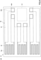
- FIG. 6 is a plan view illustrating a strain gauge according to a modified example 2 of the first embodiment.
- the cross-sectional structure of the strain gauge according to the modified example 2 of the first embodiment is the same as that in FIG. 2 , and hence, illustration of the cross-sectional view is omitted.
- a strain gauge 1B has multiple sets of resistors 30, wiring patterns 40, and electrodes 40A, and in this regard, differs from the strain gauge 1 (see FIGs. 1 and 2 ).
- the strain gauge 1B has three sets of resistors 30, wiring patterns 40, and electrodes 40A, but is not limited as such; the strain gauge according to the present example may have two sets of resistors 30, wiring patterns 40, and electrodes 40A, or may have four sets or more. Also, the number of resistors 30 and the number of electrodes 40A do not need to be the same.
- each resistor 30 may be connected by wiring patterns 40 to form a Wheatstone bridge circuit.
- four connection points of any two resistors 30 are connected to the electrodes 40A via the wiring patterns 40, respectively.
- the grid direction of each resistor 30 in FIG. 7 is an example, and is not limited as such.
- position determination marks 105 are formed near four corners in the electronic component mounting area 101.
- the position determination marks 105 are marks used for determining a position when mounting an electronic component on the electronic component mounting area 101.
- the position determination marks 105 can be formed, for example, in the same process with the resistors 30, the wiring patterns 40, and the electrodes 40A.
- the position determination marks 105 may be formed as needed, and the formation of the position determination marks 105 is not mandatory.
- a cover layer 60A may be provided on the upper surface 10a of the substrate 10, so as to cover the resistors 30 and the wiring patterns 40, and to expose the electrodes 40A and the electronic component mounting area 101.
- the material, thickness, and manufacturing method of the cover layer 60A are as described above.
- strain gauge 1B or 1C multiple sets of the resistors 30, the wiring patterns 40, and the electrodes 40A; and the electronic component mounting area 101 are provided on the upper surface 10a of one substrate 10. This enables to implement the strain gauge 1B or 1C that has a small size, and is capable of detecting strains in multiple areas. The other effects are substantially the same as in the first embodiment.
- a strain gauge In a modified example 3 of the first embodiment, an example of a strain gauge will be described in which multiple sets of resistors and the like are provided, and an electronic component is mounted on an electronic component mounting area. Note that in the modified example 3 of the first embodiment, description of the same components as those already described may be omitted.
- FIG. 8 is a plan view illustrating a strain gauge according to the modified example 3 of the first embodiment.
- the cross-sectional structure of the strain gauge according to the modified example 3 of the first embodiment is the same as that in FIG. 5 , and hence, illustration of the cross-sectional view is omitted.
- a strain gauge 1D has an electronic component 200 mounted on the electronic component mounting area 101 of the strain gauge 1B.
- the electronic component 200 is, for example, a semiconductor chip that performs amplification of an electric signal input from the resistor 30 via the wiring patterns 40 and the electrodes 40A; and temperature correction, and has a function of independently processing electric signals input from the multiple resistors 30.
- a passive component such as a capacitor may be mounted together with the semiconductor chip.
- the electronic component 200 is mounted on the electronic component mounting area 101 demarcated on the upper surface 10a of the substrate 10, via an adhesive layer such as a die attach film.
- Each electrode 200A of the electronic component 200 is electrically connected to an electrode 40A of a corresponding set via a metal wire 210 such as a gold wire or a copper wire.
- the electrodes 200A and the electrodes 40A can be connected by, for example, wire bonding.
- electronic components may be individually mounted for the respective sets of the resistors 30, the wiring patterns 40, and the electrodes 40A.
- a cover layer 60A may be provided on the upper surface 10a of the substrate 10, so as to cover the resistor 30 and the wiring patterns 40, and to expose the electrodes 40A and the electronic component mounting area 101.
- a cover layer 60B may be provided on the upper surface 10a of the substrate 10, so as to cover the resistor 30, the wiring patterns 40, the electrodes 40A, the electronic component 200, and the metal wires 210.
- a cover layer 60A may be provided on the upper surface 10a of the substrate 10, so as to cover the resistor 30 and the wiring patterns 40, and to expose the electrodes 40A and the electronic component mounting area 101; and a cover layer 60B may be further provided so as to cover the cover layer 60A, the electrodes 40A, the electronic component 200, and the metal wires 210.
- the material, thickness, and manufacturing method of the cover layers 60A and 60B are as described above.
- a strain gauge 1C may be used instead of a strain gauge 1B.
- the strain gauge 1D multiple sets of the resistor 30, the wiring patterns 40, and the electrodes 40A; and the electronic component 200 are provided on the upper surface 10a of one substrate 10.
- the electrodes 200A of the electronic component 200 and the electrodes 40A of each set can be connected within a short distance by the metal wire 210; therefore, the distance from the resistor 30 of each set to the electronic component 200 can be shortened, and the strain gauge 1D can be implemented to have a small size, and is capable of detecting strains in multiple areas.
- the other effects are substantially the same as in the modified example 1 of the first embodiment.
- the electronic component 200 may be flip-chip mounted on the upper surface 10a of the substrate 10.
- the layout of the wiring patterns 40 in each set is changed so that the electrodes 40A in the set are arranged within the electronic component mounting area 101, and the electrodes 40A of the set and the electrodes 200A of the electronic component 200 in the electronic component mounting area 101 can be connected to each other by using solder balls or the like.
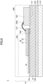
- FIG. 9 is a cross-sectional view illustrating a sensor module according to the second embodiment, which illustrates a cross section corresponding to FIG. 5 .
- a sensor module 5 includes a strain gauge 1A, a strain generator 510, and an adhesive layer 520.
- an upper surface 510a of the strain generator 510 is fixed to a lower surface 10b of the substrate 10 via the adhesive layer 520.
- the strain generator 510 is, for example, an object formed from a metal such as Fe, SUS (stainless steel), or Al; or a resin such as PEEK, and deforms (generates a strain) in response to an applied force.
- the strain gauge 1A can detect a strain generated in the strain generator 510 as a change in the resistance value of the resistor 30.
- the material of the adhesive layer 520 is not limited in particular, and can be appropriately selected depending on the purpose as long as having a function of adhering the strain gauge 1A with the strain generator 510; for example, an epoxy resin, modified epoxy resin, silicone resin, modified silicone resin, urethane resin, modified urethane resin, or the like can be used. Also, a material such as a bonding sheet may be used.
- the thickness of the adhesive layer 520 is not limited in particular and can be selected appropriately depending on the purpose; for example, the thickness can be approximately 0.1 um to 50 um.
- any one of the materials described above serving as the adhesive layer 520 is applied to the lower surface 10b of the substrate 10 and/or the upper surface 510a of the strain generator 510. Then, the lower surface 10b of the substrate 10 is faced to the upper surface 510a of the strain generator 510, and the strain gauge 1A is arranged on the strain generator 510 having the applied material interposed in-between. Alternatively, a bonding sheet may be sandwiched between the strain generator 510 and the substrate 10.
- the strain gauge 1A is heated up to a predetermined temperature while being pressed against the strain generator 510, and the applied material is cured to form the adhesive layer 520.
- the sensor module 5 can be applied to, for example, measurement of load, pressure, torque, acceleration, and the like.
- a strain gauge 1, 1B, 1C, or 1D may be used instead of the strain gauge 1A.
- the cover layer 60A may be provided as necessary, the cover layer 60B is not provided.
Landscapes
- Physics & Mathematics (AREA)
- Engineering & Computer Science (AREA)
- Microelectronics & Electronic Packaging (AREA)
- General Physics & Mathematics (AREA)
- Electromagnetism (AREA)
- Chemical & Material Sciences (AREA)
- Analytical Chemistry (AREA)
- Measurement Of Length, Angles, Or The Like Using Electric Or Magnetic Means (AREA)
Claims (14)
- Dehnungsmesser (1, 1A, 1B, 1C, 1D), umfassend:ein Substrat (10), das aus Harz gebildet ist und Flexibilität aufweist;einen Widerstand (30), der als Film gebildet ist;ein Paar von Verdrahtungsmustern (40), das elektrisch mit beiden Enden des Widerstands (30) verbunden ist;
undein Paar von Elektroden (40A, 200A), das jeweils mit dem Paar von Verdrahtungsmustern (40) elektrisch verbunden ist,wobei auf dem Substrat (10) ein Montagebereich (101) für elektronische Komponenten abgegrenzt ist, auf dem eine elektronische Komponente (200), die elektrisch mit den Elektroden (40A, 200A) verbunden ist, montiert ist,wobei der Dehnungsmesser (1, 1A, 1B, 1C, 1D) dadurch gekennzeichnet ist, dass er ferner eine Funktionsschicht (20) umfasst, die aus einem Metall, einer Legierung oder einer Metallverbindung direkt auf einer Oberfläche (10a) des Substrats (10) gebildet ist,wobei der Widerstand (30) als ein Film, der Cr, CrN und Cr2N enthält, auf einer Oberfläche der Funktionsschicht (20) gebildet ist,wobei das Paar von Verdrahtungsmustern (40) auf der einen Oberfläche der Funktionsschicht (20) gebildet ist,wobei das Paar von Elektroden (40A, 200A) auf der einen Oberfläche der Funktionsschicht (20) gebildet ist,wobei die Verdrahtungsmuster (40) eine erste Schicht (41) beinhalten, die sich von dem Widerstand (30) aus erstreckt, und eine zweite Schicht (42), die einen geringeren Widerstand als die erste Schicht (41) aufweist und auf die erste Schicht (41) geschichtet ist, undwobei die Funktionsschicht (20) ein Material beinhaltet, das die Förderung des Kristallwachstums des Widerstands (30) ermöglicht, und das Kristallwachstum bewirkt, dass der Film des Widerstands (30), der mit einer Hauptkomponente gebildet ist, gebildet wird. - Dehnungsmesser (1, 1A, 1B, 1C, 1D) nach Anspruch 1, wobei ein Element, das in der Funktionsschicht (20) enthalten ist, in den Film des Widerstands (30) diffundiert, der Cr, CrN und Cr2N enthält, und
wobei ein Dehnungsfaktor des Dehnungsmessers (1, 1A, 1B, 1C, 1D) größer oder gleich 10 ist. - Dehnungsmesser (1, 1A, 1B, 1C, 1D) nach Anspruch 1, wobei ein Element, das in der Funktionsschicht (20) enthalten ist, in den Film des Widerstands (30) diffundiert, der Cr, CrN und Cr2N enthält, und
wobei ein Temperaturkoeffizient des Widerstands in einem Bereich von -1000 ppm/°C bis +1000 ppm/°C liegt. - Dehnungsmesser (1, 1A, 1B, 1C, 1D) nach einem der Ansprüche 1 bis 3,
wobei die Funktionsschicht (20) eine oder mehrere Arten von Metallen enthält, die aus einer Gruppe ausgewählt sind, bestehend aus Cr, Ti, V, Nb, Ta, Ni, Y, Zr, Hf, Si, C, Zn, Cu, Bi, Fe, Mo, W, Ru, Rh, Re, Os, Ir, Pt, Pd, Ag, Au, Co, Mn und Al; einer Legierung aus einem der Metalle in der Gruppe; oder einer Verbindung aus einem der Metalle in der Gruppe. - Dehnungsmesser (1, 1A, 1B, 1C, 1D) nach einem der Ansprüche 1 bis 3, wobei die Hauptkomponente des Films des Widerstands (30), der Cr, CrN und Cr2N enthält, α-Cr ist und wobei die Funktionsschicht (20) eine oder mehrere Arten von Metallen enthält, die aus einer Gruppe ausgewählt sind, bestehend aus Cr, Ti, V, Nb, Ta, Ni, Y, Zr, Hf, Si, C, Zn, Cu, Bi, Fe, Mo, W, Ru, Rh, Re, Os, Ir, Pt, Pd, Ag, Au, Co, Mn und Al; einer Legierung aus einem der Metalle in der Gruppe; oder einer Verbindung aus einem der Metalle in der Gruppe.
- Dehnungsmessser (1, 1A, 1B, 1C, 1D) nach Anspruch 4 oder 5, wobei die Funktionsschicht (20) eine oder mehrere Arten von Metallen enthält, die aus einer Gruppe ausgewählt sind, bestehend aus Cr, V, Nb, Ta, Ni, Y, Hf, C, Zn, Bi, Fe, Mo, W, Ru, Rh, Re, Os, Ir, Pt, Pd, Ag, Au, Co, und Mn; einer Legierung aus einem der Metalle in der Gruppe; oder einer Verbindung aus einem der Metalle in der Gruppe.
- Dehnungsmesser (1, 1A, 1B, 1C, 1D) nach Anspruch 4 oder 5, wobei die Funktionsschicht (20) eine Art von Metallverbindung enthält, die aus einer Gruppe ausgewählt ist, bestehend aus TiN, TaN, Si3N4, TiO2, Ta2O5 und SiO2.
- Dehnungsmesser (1, 1A, 1B, 1C, 1D) nach Anspruch 7, wobei die Funktionsschicht (20) eine Art von Metallverbindung enthält, die aus einer Gruppe ausgewählt ist, bestehend aus TiN, TaN, Si3N4 und Ta2O5.
- Dehnungsmesser (1, 1A, 1B, 1C, 1D) nach Anspruch 4 oder 5, wobei die Funktionsschicht (20) eine Art von Legierung enthält, die aus einer Gruppe ausgewählt ist, bestehend aus FeCr, TiAl, FeNi, NiCr, und CrCu.
- Dehnungsmesser (1, 1A, 1B, 1C, 1D) nach einem der Ansprüche 1 bis 3, wobei die Hauptkomponente des Films des Widerstands (30), der Cr, CrN und Cr2N enthält, α-Cr ist und wobei die Funktionsschicht (20) die Funktion aufweist, das Kristallwachstum von α-Cr zu fördern, um den Film zu bilden, in dem α-Cr die Hauptkomponente ist.
- Dehnungsmesser (1, 1A, 1B, 1C, 1D) nach einem der Ansprüche 1 bis 10, wobei die Funktionsschicht (20) eine Funktion, die Oxidation des Widerstands (30) zu verhindern; eine Funktion, die Bewegung von Sauerstoff und Wasser, die in dem Substrat (10) enthalten sind, in Richtung des Widerstands zu steuern; und eine Funktion, die Haftfähigkeit zwischen dem Substrat (10) und dem Widerstand (30) zu verbessern, aufweist.
- Dehnungsmesser (1, 1A, 1B, 1C, 1D) nach einem der Ansprüche 1 bis 11,
wobei die Funktionsschicht (20) in die gleiche planare Form wie der Widerstand gemustert wird. - Dehnungsmesser (1, 1A, 1B, 1C, 1D) nach einem der Ansprüche 1 bis 12,
wobei eine Dicke der Funktionsschicht (20) 1 nm bis 100 nm beträgt. - Sensormodul (5), umfassend:den Dehnungsmesser (1, 1A, 1B, 1C, 1D) nach einem der Ansprüche 1 bis 13; undeinen Dehnungsgenerator (510), der auf einer anderen Oberflächenseite des Substrats (10) bereitgestellt ist.
Applications Claiming Priority (2)
| Application Number | Priority Date | Filing Date | Title |
|---|---|---|---|
| JP2017208195A JP2019078726A (ja) | 2017-10-27 | 2017-10-27 | ひずみゲージ、センサモジュール |
| PCT/JP2018/039716 WO2019082978A1 (ja) | 2017-10-27 | 2018-10-25 | ひずみゲージ、センサモジュール |
Publications (3)
| Publication Number | Publication Date |
|---|---|
| EP3702722A1 EP3702722A1 (de) | 2020-09-02 |
| EP3702722A4 EP3702722A4 (de) | 2021-07-21 |
| EP3702722B1 true EP3702722B1 (de) | 2023-10-11 |
Family
ID=66246945
Family Applications (1)
| Application Number | Title | Priority Date | Filing Date |
|---|---|---|---|
| EP18871642.7A Active EP3702722B1 (de) | 2017-10-27 | 2018-10-25 | Dehnungsmesser und sensormodul |
Country Status (5)
| Country | Link |
|---|---|
| US (1) | US11499876B2 (de) |
| EP (1) | EP3702722B1 (de) |
| JP (3) | JP2019078726A (de) |
| CN (1) | CN111566435B (de) |
| WO (1) | WO2019082978A1 (de) |
Families Citing this family (13)
| Publication number | Priority date | Publication date | Assignee | Title |
|---|---|---|---|---|
| JP2019174387A (ja) * | 2018-03-29 | 2019-10-10 | ミネベアミツミ株式会社 | ひずみゲージ |
| JP2022008026A (ja) * | 2020-04-08 | 2022-01-13 | ミネベアミツミ株式会社 | ひずみゲージ |
| US12523461B2 (en) * | 2020-04-08 | 2026-01-13 | Minebea Mitsumi Inc. | Strain gauge |
| JP7737790B2 (ja) * | 2020-10-16 | 2025-09-11 | ミネベアミツミ株式会社 | ひずみゲージ |
| CN113063342B (zh) * | 2021-03-22 | 2022-06-07 | 华南理工大学 | 基于同种导电材料的柔性应变传感器及其制备方法 |
| US12329504B2 (en) | 2021-05-26 | 2025-06-17 | Minebea Mitsumi Inc. | Vital sensor |
| JP7537836B2 (ja) * | 2021-05-26 | 2024-08-21 | ミネベアミツミ株式会社 | バイタルセンサ |
| JP2023072961A (ja) * | 2021-11-15 | 2023-05-25 | ミネベアミツミ株式会社 | ひずみゲージの抵抗値調整方法、ひずみゲージ |
| US12050142B2 (en) | 2022-04-05 | 2024-07-30 | Sensordata Technologies, Inc. | Effective gauge factor utilizing integrated millivolt amplifier for strain gauge applications |
| TWI816512B (zh) * | 2022-08-15 | 2023-09-21 | 國立陽明交通大學 | 曲面量測裝置、其向量感測器及製法 |
| CN115323337B (zh) * | 2022-10-11 | 2023-01-10 | 松诺盟科技有限公司 | 一种纳米薄膜复合应变传感器及其制备方法与应用 |
| CN116519178B (zh) * | 2023-05-18 | 2024-04-19 | 松诺盟科技有限公司 | 一种纳米薄膜应变片、轮辐力传感器及其制备方法 |
| CN120253022B (zh) * | 2025-04-14 | 2025-10-03 | 中国安全生产科学研究院 | 一种用于相似模拟实验的应力传感器制作及其使用方法 |
Family Cites Families (34)
| Publication number | Priority date | Publication date | Assignee | Title |
|---|---|---|---|---|
| EP0053337B1 (de) * | 1980-11-29 | 1987-05-20 | Tokyo Electric Co., Ltd. | Lastmessvorrichtung und ihr Herstellungsverfahren |
| JPS58118930A (ja) * | 1982-01-08 | 1983-07-15 | Toshiba Corp | ロ−ドセル |
| JPS59230101A (ja) * | 1983-06-13 | 1984-12-24 | Tokyo Electric Co Ltd | 歪センサ |
| DE3429649A1 (de) * | 1984-08-11 | 1986-02-20 | Vdo Adolf Schindling Ag, 6000 Frankfurt | Elektrischer widerstand |
| US4677413A (en) * | 1984-11-20 | 1987-06-30 | Vishay Intertechnology, Inc. | Precision power resistor with very low temperature coefficient of resistance |
| JPS61176803A (ja) * | 1985-01-31 | 1986-08-08 | Hitachi Ltd | ストレインゲージ |
| JPS62226029A (ja) * | 1986-03-28 | 1987-10-05 | Tokyo Electric Co Ltd | ロ−ドセルの温度補正方法 |
| US5079535A (en) * | 1990-09-11 | 1992-01-07 | Case Western Reserve University | Strain gauge and method of making and using the same |
| US5328551A (en) * | 1992-10-28 | 1994-07-12 | Eaton Corporation | Method of making high output strain gage |
| JPH06300649A (ja) * | 1993-04-12 | 1994-10-28 | Sumitomo Electric Ind Ltd | 薄膜歪抵抗材料とその製造方法及び薄膜歪みセンサ |
| JPH06307950A (ja) * | 1993-04-20 | 1994-11-04 | Tokyo Electric Co Ltd | 歪センサ |
| JP3233248B2 (ja) * | 1994-05-13 | 2001-11-26 | エヌオーケー株式会社 | 歪ゲ−ジ用薄膜およびその製造法 |
| JPH08102163A (ja) * | 1994-09-30 | 1996-04-16 | Fujitsu Ltd | 磁気記録媒体及び磁気ディスク装置 |
| EP0725392A1 (de) * | 1995-01-31 | 1996-08-07 | Hoya Corporation | Magnetisches Aufzeichnungsmedium sowie Verfahren zu seiner Herstellung |
| JP3642449B2 (ja) * | 1997-03-21 | 2005-04-27 | 財団法人電気磁気材料研究所 | Cr−N基歪抵抗膜およびその製造法ならびに歪センサ |
| JP2001338382A (ja) | 2000-05-29 | 2001-12-07 | Takenaka Komuten Co Ltd | 計測装置及びモニタリングシステム |
| JP2002221453A (ja) * | 2001-01-29 | 2002-08-09 | Nippon Denshi Kogyo Kk | 構造体の荷重情報収集装置 |
| JP2004072715A (ja) | 2002-06-11 | 2004-03-04 | Murata Mfg Co Ltd | 圧電薄膜共振子、圧電フィルタ、およびそれを有する電子部品 |
| EP1384980A1 (de) * | 2002-07-25 | 2004-01-28 | Mettler-Toledo GmbH | Feuchtigkeitsschutz für einen elektromechanischen Wandler |
| CN100413998C (zh) * | 2002-08-08 | 2008-08-27 | 株式会社神户制钢所 | α型晶体结构为主体的氧化铝被膜相关技术 |
| JP2004205410A (ja) | 2002-12-26 | 2004-07-22 | Takata Corp | 荷重センサ及びシート重量計測装置 |
| ATE461437T1 (de) * | 2004-01-27 | 2010-04-15 | Mettler Toledo Ag | Dehnmessstreifen mit feuchtigkeitsschutz durch inhomogene anorganische schicht auf glättender polymerschicht (ormocer) und schlitzanordnung |
| JP2005233953A (ja) * | 2004-02-17 | 2005-09-02 | Robert Bosch Gmbh | マイクロメカニカル式の高圧センサを製造するための方法及びマクロメカニカル式の圧力センサ |
| JP2007173544A (ja) * | 2005-12-22 | 2007-07-05 | Toshiba Corp | X線検出器およびその製造方法 |
| JP2012208032A (ja) * | 2011-03-30 | 2012-10-25 | Minebea Co Ltd | ひずみゲージおよびその製造方法 |
| JP6159613B2 (ja) * | 2013-08-05 | 2017-07-05 | 公益財団法人電磁材料研究所 | 歪センサ |
| JP6162670B2 (ja) | 2014-10-03 | 2017-07-12 | 株式会社東京測器研究所 | ひずみゲージ用合金及びひずみゲージ |
| JP6256360B2 (ja) * | 2015-01-23 | 2018-01-10 | 株式会社豊田中央研究所 | 永久磁石およびその製造方法 |
| JP2017067764A (ja) | 2015-09-29 | 2017-04-06 | ミネベアミツミ株式会社 | ひずみゲージ、荷重センサ、及びひずみゲージの製造方法 |
| JP2017101983A (ja) * | 2015-12-01 | 2017-06-08 | 日本写真印刷株式会社 | 多点計測用のひずみセンサとその製造方法 |
| JP6829947B2 (ja) | 2016-05-17 | 2021-02-17 | ローム株式会社 | 発光素子駆動用半導体集積回路、発光素子駆動装置、発光装置、車両 |
| JP2019066453A (ja) * | 2017-09-29 | 2019-04-25 | ミネベアミツミ株式会社 | ひずみゲージ |
| JP2019066454A (ja) * | 2017-09-29 | 2019-04-25 | ミネベアミツミ株式会社 | ひずみゲージ、センサモジュール |
| JP2020129013A (ja) * | 2020-06-05 | 2020-08-27 | ミネベアミツミ株式会社 | ひずみゲージ |
-
2017
- 2017-10-27 JP JP2017208195A patent/JP2019078726A/ja active Pending
-
2018
- 2018-10-25 CN CN201880083538.XA patent/CN111566435B/zh active Active
- 2018-10-25 WO PCT/JP2018/039716 patent/WO2019082978A1/ja not_active Ceased
- 2018-10-25 EP EP18871642.7A patent/EP3702722B1/de active Active
- 2018-10-25 US US16/757,869 patent/US11499876B2/en active Active
-
2023
- 2023-05-31 JP JP2023090067A patent/JP2023101720A/ja active Pending
-
2025
- 2025-05-20 JP JP2025083845A patent/JP7820595B2/ja active Active
Also Published As
| Publication number | Publication date |
|---|---|
| US11499876B2 (en) | 2022-11-15 |
| JP2019078726A (ja) | 2019-05-23 |
| CN111566435B (zh) | 2023-04-18 |
| WO2019082978A1 (ja) | 2019-05-02 |
| EP3702722A1 (de) | 2020-09-02 |
| JP2025109905A (ja) | 2025-07-25 |
| US20210063258A1 (en) | 2021-03-04 |
| JP2023101720A (ja) | 2023-07-21 |
| JP7820595B2 (ja) | 2026-02-25 |
| EP3702722A4 (de) | 2021-07-21 |
| CN111566435A (zh) | 2020-08-21 |
Similar Documents
| Publication | Publication Date | Title |
|---|---|---|
| EP3702722B1 (de) | Dehnungsmesser und sensormodul | |
| US11499877B2 (en) | Strain gauge | |
| US12523556B2 (en) | Strain gauge | |
| US11448560B2 (en) | Strain gauge and sensor module | |
| US11454489B2 (en) | Sensor module with reduced size | |
| US10921110B2 (en) | Strain gauge | |
| EP4261494B1 (de) | Dehnungsmesser | |
| CN115298511A (zh) | 应变片 | |
| WO2019244990A1 (ja) | ひずみゲージ | |
| JP2023138686A (ja) | センサモジュール | |
| JP7755708B2 (ja) | ひずみゲージ | |
| US20240369429A1 (en) | Strain gauge | |
| JP7303663B2 (ja) | ひずみゲージ、センサモジュール、接続構造 | |
| JP2022008026A (ja) | ひずみゲージ | |
| US12595998B2 (en) | Strain gauge | |
| CN119137441B (zh) | 应变计 |
Legal Events
| Date | Code | Title | Description |
|---|---|---|---|
| STAA | Information on the status of an ep patent application or granted ep patent |
Free format text: STATUS: THE INTERNATIONAL PUBLICATION HAS BEEN MADE |
|
| PUAI | Public reference made under article 153(3) epc to a published international application that has entered the european phase |
Free format text: ORIGINAL CODE: 0009012 |
|
| STAA | Information on the status of an ep patent application or granted ep patent |
Free format text: STATUS: REQUEST FOR EXAMINATION WAS MADE |
|
| 17P | Request for examination filed |
Effective date: 20200515 |
|
| AK | Designated contracting states |
Kind code of ref document: A1 Designated state(s): AL AT BE BG CH CY CZ DE DK EE ES FI FR GB GR HR HU IE IS IT LI LT LU LV MC MK MT NL NO PL PT RO RS SE SI SK SM TR |
|
| AX | Request for extension of the european patent |
Extension state: BA ME |
|
| DAV | Request for validation of the european patent (deleted) | ||
| DAX | Request for extension of the european patent (deleted) | ||
| A4 | Supplementary search report drawn up and despatched |
Effective date: 20210622 |
|
| RIC1 | Information provided on ipc code assigned before grant |
Ipc: G01B 7/16 20060101AFI20210616BHEP |
|
| GRAP | Despatch of communication of intention to grant a patent |
Free format text: ORIGINAL CODE: EPIDOSNIGR1 |
|
| STAA | Information on the status of an ep patent application or granted ep patent |
Free format text: STATUS: GRANT OF PATENT IS INTENDED |
|
| INTG | Intention to grant announced |
Effective date: 20230504 |
|
| RIN1 | Information on inventor provided before grant (corrected) |
Inventor name: KIMURA, YOICHI Inventor name: IIJIMA, HIROTSUGU Inventor name: ASAKAWA, TOSHIAKI Inventor name: KITAMURA, ATSUSHI Inventor name: MISAIZU, EIJI Inventor name: ADACHI, SHIGEYUKI Inventor name: SATO, SATOSHI |
|
| GRAS | Grant fee paid |
Free format text: ORIGINAL CODE: EPIDOSNIGR3 |
|
| GRAA | (expected) grant |
Free format text: ORIGINAL CODE: 0009210 |
|
| STAA | Information on the status of an ep patent application or granted ep patent |
Free format text: STATUS: THE PATENT HAS BEEN GRANTED |
|
| AK | Designated contracting states |
Kind code of ref document: B1 Designated state(s): AL AT BE BG CH CY CZ DE DK EE ES FI FR GB GR HR HU IE IS IT LI LT LU LV MC MK MT NL NO PL PT RO RS SE SI SK SM TR |
|
| REG | Reference to a national code |
Ref country code: GB Ref legal event code: FG4D |
|
| REG | Reference to a national code |
Ref country code: CH Ref legal event code: EP |
|
| REG | Reference to a national code |
Ref country code: DE Ref legal event code: R096 Ref document number: 602018059355 Country of ref document: DE |
|
| REG | Reference to a national code |
Ref country code: IE Ref legal event code: FG4D |
|
| REG | Reference to a national code |
Ref country code: LT Ref legal event code: MG9D |
|
| REG | Reference to a national code |
Ref country code: NL Ref legal event code: MP Effective date: 20231011 |
|
| REG | Reference to a national code |
Ref country code: AT Ref legal event code: MK05 Ref document number: 1620611 Country of ref document: AT Kind code of ref document: T Effective date: 20231011 |
|
| PG25 | Lapsed in a contracting state [announced via postgrant information from national office to epo] |
Ref country code: NL Free format text: LAPSE BECAUSE OF FAILURE TO SUBMIT A TRANSLATION OF THE DESCRIPTION OR TO PAY THE FEE WITHIN THE PRESCRIBED TIME-LIMIT Effective date: 20231011 |
|
| PG25 | Lapsed in a contracting state [announced via postgrant information from national office to epo] |
Ref country code: GR Free format text: LAPSE BECAUSE OF FAILURE TO SUBMIT A TRANSLATION OF THE DESCRIPTION OR TO PAY THE FEE WITHIN THE PRESCRIBED TIME-LIMIT Effective date: 20240112 |
|
| PG25 | Lapsed in a contracting state [announced via postgrant information from national office to epo] |
Ref country code: IS Free format text: LAPSE BECAUSE OF FAILURE TO SUBMIT A TRANSLATION OF THE DESCRIPTION OR TO PAY THE FEE WITHIN THE PRESCRIBED TIME-LIMIT Effective date: 20240211 |
|
| PG25 | Lapsed in a contracting state [announced via postgrant information from national office to epo] |
Ref country code: LT Free format text: LAPSE BECAUSE OF FAILURE TO SUBMIT A TRANSLATION OF THE DESCRIPTION OR TO PAY THE FEE WITHIN THE PRESCRIBED TIME-LIMIT Effective date: 20231011 |
|
| PG25 | Lapsed in a contracting state [announced via postgrant information from national office to epo] |
Ref country code: AT Free format text: LAPSE BECAUSE OF FAILURE TO SUBMIT A TRANSLATION OF THE DESCRIPTION OR TO PAY THE FEE WITHIN THE PRESCRIBED TIME-LIMIT Effective date: 20231011 |
|
| PG25 | Lapsed in a contracting state [announced via postgrant information from national office to epo] |
Ref country code: ES Free format text: LAPSE BECAUSE OF FAILURE TO SUBMIT A TRANSLATION OF THE DESCRIPTION OR TO PAY THE FEE WITHIN THE PRESCRIBED TIME-LIMIT Effective date: 20231011 |
|
| PG25 | Lapsed in a contracting state [announced via postgrant information from national office to epo] |
Ref country code: LT Free format text: LAPSE BECAUSE OF FAILURE TO SUBMIT A TRANSLATION OF THE DESCRIPTION OR TO PAY THE FEE WITHIN THE PRESCRIBED TIME-LIMIT Effective date: 20231011 Ref country code: IS Free format text: LAPSE BECAUSE OF FAILURE TO SUBMIT A TRANSLATION OF THE DESCRIPTION OR TO PAY THE FEE WITHIN THE PRESCRIBED TIME-LIMIT Effective date: 20240211 Ref country code: GR Free format text: LAPSE BECAUSE OF FAILURE TO SUBMIT A TRANSLATION OF THE DESCRIPTION OR TO PAY THE FEE WITHIN THE PRESCRIBED TIME-LIMIT Effective date: 20240112 Ref country code: ES Free format text: LAPSE BECAUSE OF FAILURE TO SUBMIT A TRANSLATION OF THE DESCRIPTION OR TO PAY THE FEE WITHIN THE PRESCRIBED TIME-LIMIT Effective date: 20231011 Ref country code: BG Free format text: LAPSE BECAUSE OF FAILURE TO SUBMIT A TRANSLATION OF THE DESCRIPTION OR TO PAY THE FEE WITHIN THE PRESCRIBED TIME-LIMIT Effective date: 20240111 Ref country code: AT Free format text: LAPSE BECAUSE OF FAILURE TO SUBMIT A TRANSLATION OF THE DESCRIPTION OR TO PAY THE FEE WITHIN THE PRESCRIBED TIME-LIMIT Effective date: 20231011 Ref country code: PT Free format text: LAPSE BECAUSE OF FAILURE TO SUBMIT A TRANSLATION OF THE DESCRIPTION OR TO PAY THE FEE WITHIN THE PRESCRIBED TIME-LIMIT Effective date: 20240212 |
|
| PG25 | Lapsed in a contracting state [announced via postgrant information from national office to epo] |
Ref country code: SE Free format text: LAPSE BECAUSE OF FAILURE TO SUBMIT A TRANSLATION OF THE DESCRIPTION OR TO PAY THE FEE WITHIN THE PRESCRIBED TIME-LIMIT Effective date: 20231011 Ref country code: RS Free format text: LAPSE BECAUSE OF FAILURE TO SUBMIT A TRANSLATION OF THE DESCRIPTION OR TO PAY THE FEE WITHIN THE PRESCRIBED TIME-LIMIT Effective date: 20231011 Ref country code: PL Free format text: LAPSE BECAUSE OF FAILURE TO SUBMIT A TRANSLATION OF THE DESCRIPTION OR TO PAY THE FEE WITHIN THE PRESCRIBED TIME-LIMIT Effective date: 20231011 Ref country code: NO Free format text: LAPSE BECAUSE OF FAILURE TO SUBMIT A TRANSLATION OF THE DESCRIPTION OR TO PAY THE FEE WITHIN THE PRESCRIBED TIME-LIMIT Effective date: 20240111 Ref country code: LV Free format text: LAPSE BECAUSE OF FAILURE TO SUBMIT A TRANSLATION OF THE DESCRIPTION OR TO PAY THE FEE WITHIN THE PRESCRIBED TIME-LIMIT Effective date: 20231011 Ref country code: HR Free format text: LAPSE BECAUSE OF FAILURE TO SUBMIT A TRANSLATION OF THE DESCRIPTION OR TO PAY THE FEE WITHIN THE PRESCRIBED TIME-LIMIT Effective date: 20231011 |
|
| REG | Reference to a national code |
Ref country code: CH Ref legal event code: PL |
|
| REG | Reference to a national code |
Ref country code: BE Ref legal event code: MM Effective date: 20231031 |
|
| PG25 | Lapsed in a contracting state [announced via postgrant information from national office to epo] |
Ref country code: LU Free format text: LAPSE BECAUSE OF NON-PAYMENT OF DUE FEES Effective date: 20231025 |
|
| PG25 | Lapsed in a contracting state [announced via postgrant information from national office to epo] |
Ref country code: LU Free format text: LAPSE BECAUSE OF NON-PAYMENT OF DUE FEES Effective date: 20231025 |
|
| PG25 | Lapsed in a contracting state [announced via postgrant information from national office to epo] |
Ref country code: DK Free format text: LAPSE BECAUSE OF FAILURE TO SUBMIT A TRANSLATION OF THE DESCRIPTION OR TO PAY THE FEE WITHIN THE PRESCRIBED TIME-LIMIT Effective date: 20231011 |
|
| REG | Reference to a national code |
Ref country code: DE Ref legal event code: R097 Ref document number: 602018059355 Country of ref document: DE |
|
| PG25 | Lapsed in a contracting state [announced via postgrant information from national office to epo] |
Ref country code: CH Free format text: LAPSE BECAUSE OF NON-PAYMENT OF DUE FEES Effective date: 20231031 |
|
| PG25 | Lapsed in a contracting state [announced via postgrant information from national office to epo] |
Ref country code: CZ Free format text: LAPSE BECAUSE OF FAILURE TO SUBMIT A TRANSLATION OF THE DESCRIPTION OR TO PAY THE FEE WITHIN THE PRESCRIBED TIME-LIMIT Effective date: 20231011 |
|
| PG25 | Lapsed in a contracting state [announced via postgrant information from national office to epo] |
Ref country code: SK Free format text: LAPSE BECAUSE OF FAILURE TO SUBMIT A TRANSLATION OF THE DESCRIPTION OR TO PAY THE FEE WITHIN THE PRESCRIBED TIME-LIMIT Effective date: 20231011 |
|
| PG25 | Lapsed in a contracting state [announced via postgrant information from national office to epo] |
Ref country code: SM Free format text: LAPSE BECAUSE OF FAILURE TO SUBMIT A TRANSLATION OF THE DESCRIPTION OR TO PAY THE FEE WITHIN THE PRESCRIBED TIME-LIMIT Effective date: 20231011 Ref country code: SK Free format text: LAPSE BECAUSE OF FAILURE TO SUBMIT A TRANSLATION OF THE DESCRIPTION OR TO PAY THE FEE WITHIN THE PRESCRIBED TIME-LIMIT Effective date: 20231011 Ref country code: RO Free format text: LAPSE BECAUSE OF FAILURE TO SUBMIT A TRANSLATION OF THE DESCRIPTION OR TO PAY THE FEE WITHIN THE PRESCRIBED TIME-LIMIT Effective date: 20231011 Ref country code: IT Free format text: LAPSE BECAUSE OF FAILURE TO SUBMIT A TRANSLATION OF THE DESCRIPTION OR TO PAY THE FEE WITHIN THE PRESCRIBED TIME-LIMIT Effective date: 20231011 Ref country code: EE Free format text: LAPSE BECAUSE OF FAILURE TO SUBMIT A TRANSLATION OF THE DESCRIPTION OR TO PAY THE FEE WITHIN THE PRESCRIBED TIME-LIMIT Effective date: 20231011 Ref country code: DK Free format text: LAPSE BECAUSE OF FAILURE TO SUBMIT A TRANSLATION OF THE DESCRIPTION OR TO PAY THE FEE WITHIN THE PRESCRIBED TIME-LIMIT Effective date: 20231011 Ref country code: CZ Free format text: LAPSE BECAUSE OF FAILURE TO SUBMIT A TRANSLATION OF THE DESCRIPTION OR TO PAY THE FEE WITHIN THE PRESCRIBED TIME-LIMIT Effective date: 20231011 Ref country code: CH Free format text: LAPSE BECAUSE OF NON-PAYMENT OF DUE FEES Effective date: 20231031 |
|
| PLBE | No opposition filed within time limit |
Free format text: ORIGINAL CODE: 0009261 |
|
| STAA | Information on the status of an ep patent application or granted ep patent |
Free format text: STATUS: NO OPPOSITION FILED WITHIN TIME LIMIT |
|
| PG25 | Lapsed in a contracting state [announced via postgrant information from national office to epo] |
Ref country code: MC Free format text: LAPSE BECAUSE OF FAILURE TO SUBMIT A TRANSLATION OF THE DESCRIPTION OR TO PAY THE FEE WITHIN THE PRESCRIBED TIME-LIMIT Effective date: 20231011 |
|
| PG25 | Lapsed in a contracting state [announced via postgrant information from national office to epo] |
Ref country code: MC Free format text: LAPSE BECAUSE OF FAILURE TO SUBMIT A TRANSLATION OF THE DESCRIPTION OR TO PAY THE FEE WITHIN THE PRESCRIBED TIME-LIMIT Effective date: 20231011 Ref country code: BE Free format text: LAPSE BECAUSE OF NON-PAYMENT OF DUE FEES Effective date: 20231031 |
|
| 26N | No opposition filed |
Effective date: 20240712 |
|
| PG25 | Lapsed in a contracting state [announced via postgrant information from national office to epo] |
Ref country code: IE Free format text: LAPSE BECAUSE OF NON-PAYMENT OF DUE FEES Effective date: 20231025 |
|
| PG25 | Lapsed in a contracting state [announced via postgrant information from national office to epo] |
Ref country code: SI Free format text: LAPSE BECAUSE OF FAILURE TO SUBMIT A TRANSLATION OF THE DESCRIPTION OR TO PAY THE FEE WITHIN THE PRESCRIBED TIME-LIMIT Effective date: 20231011 |
|
| PG25 | Lapsed in a contracting state [announced via postgrant information from national office to epo] |
Ref country code: SI Free format text: LAPSE BECAUSE OF FAILURE TO SUBMIT A TRANSLATION OF THE DESCRIPTION OR TO PAY THE FEE WITHIN THE PRESCRIBED TIME-LIMIT Effective date: 20231011 Ref country code: IE Free format text: LAPSE BECAUSE OF NON-PAYMENT OF DUE FEES Effective date: 20231025 |
|
| P01 | Opt-out of the competence of the unified patent court (upc) registered |
Free format text: CASE NUMBER: APP_52550/2024 Effective date: 20240919 |
|
| PG25 | Lapsed in a contracting state [announced via postgrant information from national office to epo] |
Ref country code: FI Free format text: LAPSE BECAUSE OF FAILURE TO SUBMIT A TRANSLATION OF THE DESCRIPTION OR TO PAY THE FEE WITHIN THE PRESCRIBED TIME-LIMIT Effective date: 20231011 |
|
| PG25 | Lapsed in a contracting state [announced via postgrant information from national office to epo] |
Ref country code: CY Free format text: LAPSE BECAUSE OF FAILURE TO SUBMIT A TRANSLATION OF THE DESCRIPTION OR TO PAY THE FEE WITHIN THE PRESCRIBED TIME-LIMIT; INVALID AB INITIO Effective date: 20181025 |
|
| PG25 | Lapsed in a contracting state [announced via postgrant information from national office to epo] |
Ref country code: HU Free format text: LAPSE BECAUSE OF FAILURE TO SUBMIT A TRANSLATION OF THE DESCRIPTION OR TO PAY THE FEE WITHIN THE PRESCRIBED TIME-LIMIT; INVALID AB INITIO Effective date: 20181025 |
|
| PG25 | Lapsed in a contracting state [announced via postgrant information from national office to epo] |
Ref country code: TR Free format text: LAPSE BECAUSE OF FAILURE TO SUBMIT A TRANSLATION OF THE DESCRIPTION OR TO PAY THE FEE WITHIN THE PRESCRIBED TIME-LIMIT Effective date: 20231011 |
|
| PGFP | Annual fee paid to national office [announced via postgrant information from national office to epo] |
Ref country code: DE Payment date: 20251021 Year of fee payment: 8 |
|
| PGFP | Annual fee paid to national office [announced via postgrant information from national office to epo] |
Ref country code: GB Payment date: 20251022 Year of fee payment: 8 |
|
| PGFP | Annual fee paid to national office [announced via postgrant information from national office to epo] |
Ref country code: FR Payment date: 20251030 Year of fee payment: 8 |