EP3694095B1 - Stromumwandlungsvorrichtung - Google Patents
Stromumwandlungsvorrichtung Download PDFInfo
- Publication number
- EP3694095B1 EP3694095B1 EP18865083.2A EP18865083A EP3694095B1 EP 3694095 B1 EP3694095 B1 EP 3694095B1 EP 18865083 A EP18865083 A EP 18865083A EP 3694095 B1 EP3694095 B1 EP 3694095B1
- Authority
- EP
- European Patent Office
- Prior art keywords
- flying capacitor
- switching element
- capacitor circuit
- switching
- voltage
- Prior art date
- Legal status (The legal status is an assumption and is not a legal conclusion. Google has not performed a legal analysis and makes no representation as to the accuracy of the status listed.)
- Active
Links
Images


Classifications
-
- H—ELECTRICITY
- H02—GENERATION; CONVERSION OR DISTRIBUTION OF ELECTRIC POWER
- H02M—APPARATUS FOR CONVERSION BETWEEN AC AND AC, BETWEEN AC AND DC, OR BETWEEN DC AND DC, AND FOR USE WITH MAINS OR SIMILAR POWER SUPPLY SYSTEMS; CONVERSION OF DC OR AC INPUT POWER INTO SURGE OUTPUT POWER; CONTROL OR REGULATION THEREOF
- H02M7/00—Conversion of AC power input into DC power output; Conversion of DC power input into AC power output
- H02M7/42—Conversion of DC power input into AC power output without possibility of reversal
- H02M7/44—Conversion of DC power input into AC power output without possibility of reversal by static converters
- H02M7/48—Conversion of DC power input into AC power output without possibility of reversal by static converters using discharge tubes with control electrode or semiconductor devices with control electrode
- H02M7/483—Converters with outputs that each can have more than two voltages levels
- H02M7/4837—Flying capacitor converters
-
- H—ELECTRICITY
- H02—GENERATION; CONVERSION OR DISTRIBUTION OF ELECTRIC POWER
- H02M—APPARATUS FOR CONVERSION BETWEEN AC AND AC, BETWEEN AC AND DC, OR BETWEEN DC AND DC, AND FOR USE WITH MAINS OR SIMILAR POWER SUPPLY SYSTEMS; CONVERSION OF DC OR AC INPUT POWER INTO SURGE OUTPUT POWER; CONTROL OR REGULATION THEREOF
- H02M7/00—Conversion of AC power input into DC power output; Conversion of DC power input into AC power output
- H02M7/42—Conversion of DC power input into AC power output without possibility of reversal
- H02M7/44—Conversion of DC power input into AC power output without possibility of reversal by static converters
- H02M7/48—Conversion of DC power input into AC power output without possibility of reversal by static converters using discharge tubes with control electrode or semiconductor devices with control electrode
- H02M7/483—Converters with outputs that each can have more than two voltages levels
- H02M7/4833—Capacitor voltage balancing
-
- H—ELECTRICITY
- H02—GENERATION; CONVERSION OR DISTRIBUTION OF ELECTRIC POWER
- H02M—APPARATUS FOR CONVERSION BETWEEN AC AND AC, BETWEEN AC AND DC, OR BETWEEN DC AND DC, AND FOR USE WITH MAINS OR SIMILAR POWER SUPPLY SYSTEMS; CONVERSION OF DC OR AC INPUT POWER INTO SURGE OUTPUT POWER; CONTROL OR REGULATION THEREOF
- H02M7/00—Conversion of AC power input into DC power output; Conversion of DC power input into AC power output
- H02M7/42—Conversion of DC power input into AC power output without possibility of reversal
- H02M7/44—Conversion of DC power input into AC power output without possibility of reversal by static converters
- H02M7/48—Conversion of DC power input into AC power output without possibility of reversal by static converters using discharge tubes with control electrode or semiconductor devices with control electrode
- H02M7/483—Converters with outputs that each can have more than two voltages levels
- H02M7/487—Neutral point clamped inverters
-
- H—ELECTRICITY
- H02—GENERATION; CONVERSION OR DISTRIBUTION OF ELECTRIC POWER
- H02M—APPARATUS FOR CONVERSION BETWEEN AC AND AC, BETWEEN AC AND DC, OR BETWEEN DC AND DC, AND FOR USE WITH MAINS OR SIMILAR POWER SUPPLY SYSTEMS; CONVERSION OF DC OR AC INPUT POWER INTO SURGE OUTPUT POWER; CONTROL OR REGULATION THEREOF
- H02M7/00—Conversion of AC power input into DC power output; Conversion of DC power input into AC power output
- H02M7/42—Conversion of DC power input into AC power output without possibility of reversal
- H02M7/44—Conversion of DC power input into AC power output without possibility of reversal by static converters
- H02M7/48—Conversion of DC power input into AC power output without possibility of reversal by static converters using discharge tubes with control electrode or semiconductor devices with control electrode
- H02M7/53—Conversion of DC power input into AC power output without possibility of reversal by static converters using discharge tubes with control electrode or semiconductor devices with control electrode using devices of a triode or transistor type requiring continuous application of a control signal
- H02M7/537—Conversion of DC power input into AC power output without possibility of reversal by static converters using discharge tubes with control electrode or semiconductor devices with control electrode using devices of a triode or transistor type requiring continuous application of a control signal using semiconductor devices only, e.g. single switched pulse inverters
-
- H—ELECTRICITY
- H02—GENERATION; CONVERSION OR DISTRIBUTION OF ELECTRIC POWER
- H02M—APPARATUS FOR CONVERSION BETWEEN AC AND AC, BETWEEN AC AND DC, OR BETWEEN DC AND DC, AND FOR USE WITH MAINS OR SIMILAR POWER SUPPLY SYSTEMS; CONVERSION OF DC OR AC INPUT POWER INTO SURGE OUTPUT POWER; CONTROL OR REGULATION THEREOF
- H02M1/00—Details of apparatus for conversion
- H02M1/0095—Hybrid converter topologies, e.g. NPC mixed with flying capacitor, thyristor converter mixed with MMC or charge pump mixed with buck
Definitions
- Fig. 2 is a circuit diagram of a power converter according to a second embodiment of the present disclosure.
- each of the switching elements S1-S4 in the output stage of the power converter 10 shown in Fig. 1 is replaced by two switching elements connected in series.
- the other features are the same as those of Fig. 1 .
- the withstand voltage of the switching elements in the output stage can be further reduced to half that of the power converter 10 shown in Fig. 1 . Therefore, the switching elements S1a-S4b in the output stage may all have a withstand voltage E/4. Therefore, all of the switching elements forming the power converter 10 shown in Fig. 2 can be a switching element having a withstand voltage E/4 [V]. If the DC power supply voltage is 600 [V], for example, all of the switching elements may be switching elements having a withstand voltage 150 [V] that are less expensive and offer high performance so that it is possible to provide a power converter that is less expensive and offers higher performance.
- Figs. 3A-3D show a first example of switching pattern in the method of controlling a power converter according to the embodiment and show switching patterns in which an output voltage having the positive polarity in the U phase and the negative polarity in the W phase is output.
- the switching elements are illustrated in a simplified fashion for ease of understanding.
- Fig. 3A shows a switching pattern (1) for outputting a +E [V] output voltage.
- the switching elements S5a and S5b of the first flying capacitor circuit 11 are turned on, and S5c and S5d are turned off to output E [V] from the first flying capacitor circuit 11.
- the switching elements S1a and S1b in the output stage are turned on, and S2a and S2b are turned off to output, from the first output end OUT1, E [V] output from the first flying capacitor circuit 11.
- the switching elements S8c and S8d of the fourth flying capacitor circuit 14 are turned on, and S8a and S8b are turned off to output 0 [V] from the fourth flying capacitor circuit 14.
- the four flying capacitors FC1-FC4 are neither charged nor discharged, and the charge is maintained.
- Fig. 3B shows a switching pattern (2) for outputting a +E/2 [V] output voltage.
- the switching elements S5a and S5c of the first flying capacitor circuit 11 are turned on, and S5b and S5d are turned off to output 3E/4 [V] from the first flying capacitor circuit 11.
- the switching elements S1a and S1b in the output stage are turned on, and S2a and S2b are turned off to output, from the first output end OUT1, 3E/4 [V] output from the first flying capacitor circuit 11.
- the switching elements S8b and S8d of the fourth flying capacitor circuit 14 are turned on, and S8a and S8c are turned off to output E/4 [V] from the fourth flying capacitor circuit 14.
- the switching elements S4a and S4b in the output stage are turned on, and S3a and S3b are turned off to output, from the second output end OUT2, E/4 [V] output from the fourth flying capacitor circuit 14. This causes +E/2 [V] to be output from the first output end OUT1 and the second output end OUT2.
- Fig. 3C shows a switching pattern (3) for outputting a +E/2 [V] output voltage.
- the switching elements S5b and S5d of the first flying capacitor circuit 11 are turned on, and S5a and S5c are turned off to output 3E/4 [V] from the first flying capacitor circuit 11.
- the switching elements S1a and S1b in the output stage are turned on, and S2a and S2b are turned off to output, from the first output end OUT1, 3E/4 [V] output from the first flying capacitor circuit 11.
- the switching elements S8a and S8c of the fourth flying capacitor circuit 14 are turned on, and S8b and S8d are turned off to output E/4 [V] from the fourth flying capacitor circuit 14.
- the switching elements S4a and S4b in the output stage are turned on, and S3a and S3b are turned off to output, from the second output end OUT2, E/4 [V] output from the fourth flying capacitor circuit 14. This causes +E/2 [V] to be output from the first output end OUT1 and the second output end OUT2.
- the flying capacitors FC1 and FC4 are discharged, and the flying capacitors FC2 and FC3 are neither charged nor discharged.
- the switching elements S4a and S4b in the output stage are turned on, and S3a and S3b are turned off to output, from the second output end OUT2, E/2 [V] output from the fourth flying capacitor circuit 14. This causes +0 [V] to be output from the first output end OUT1 and the second output end OUT2.
- the four flying capacitors FC1-FC4 are neither charged nor discharged, and the charge is maintained.
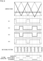
- Figs. 4A-4D show a first example of switching pattern in the method of controlling a power converter according to the embodiment and show switching patterns in which an output voltage having the negative polarity in the U phase and the positive polarity in the W phase is output.
- the switching elements are illustrated in a simplified fashion for ease of understanding.
- Fig. 4A shows a switching pattern (1) for outputting a -E [V] output voltage.
- the switching elements S6c and S6d of the second flying capacitor circuit 12 are turned on, and S6a and S6b are turned off to output 0 [V] from the second flying capacitor circuit 12.
- the switching elements S2a and S2b in the output stage are turned on, and S1a and S1b are turned off to output, from the first output end OUT1, 0 [V] output from the second flying capacitor circuit 12.
- the switching elements S7a and S7b of the third flying capacitor circuit 13 are turned on, and S7c and S7d are turned off to output E [V] from the third flying capacitor circuit 13.
- the switching elements S3a and S3b in the output stage are turned on, and S4a and S4b are turned off to output, from the second output end OUT2, E [V] output from the third flying capacitor circuit 13. This causes -E [V] to be output from the first output end OUT1 and the second output end OUT2.
- the four flying capacitors FC1-FC4 are neither charged nor discharged, and the charge is maintained.
- Fig. 4B shows a switching pattern (2) for outputting a -E/2 [V] output voltage.
- the switching elements S6b and S6d of the second flying capacitor circuit 12 are turned on, and S6a and S6c are turned off to output E/4 [V] from the second flying capacitor circuit 12.
- the switching elements S2a and S2b in the output stage are turned on, and S1a and S1b are turned off to output, from the first output end OUT1, E/4 [V] output from the second flying capacitor circuit 12.
- the switching elements S7a and S7c of the third flying capacitor circuit 13 are turned on, and S7b and S7d are turned off to output 3E/4 [V] from the third flying capacitor circuit 13.
- the switching elements S3a and S3b in the output stage are turned on, and S4a and S4b are turned off to output, from the second output end OUT2, 3E/4 [V] output from the third flying capacitor circuit 13. This causes -E/2 [V] to be output from the first output end OUT1 and the second output end OUT2.
- the flying capacitors FC2 and FC3 are charged, and the flying capacitors FC1 and FC4 are neither charged nor discharged.
- Fig. 4C shows a switching pattern (3) for outputting a -E/2 [V] output voltage.
- the switching elements S6a and S6c of the second flying capacitor circuit 12 are turned on, and S6b and S6d are turned off to output E/4 [V] from the second flying capacitor circuit 12.
- the switching elements S2a and S2b in the output stage are turned on, and S1a and S1b are turned off to output, from the first output end OUT1, E/4 [V] output from the second flying capacitor circuit 12.
- the switching elements S7b and S7d of the third flying capacitor circuit 13 are turned on, and S7a and S7c are turned off to output 3E/4 [V] from the third flying capacitor circuit 13.
- the switching elements S3a and S3b in the output stage are turned on, and S4a and S4b are turned off to output, from the second output end OUT2, 3E/4 [V] output from the third flying capacitor circuit 13. This causes -E/2 [V] to be output from the first output end OUT1 and the second output end OUT2.
- the flying capacitors FC2 and FC3 are discharged, and the flying capacitors FC1 and FC4 are neither charged nor discharged.
- Fig. 4D shows a switching pattern (4) for outputting a -0 [V] output voltage.
- the switching elements S6a and S6b of the second flying capacitor circuit 12 are turned on, and S6c and S6d are turned off to output E/2 [V] from the second flying capacitor circuit 12.
- the switching elements S2a and S2b in the output stage are turned on, and S1a and S1b are turned off to output, from the first output end OUT1, E/2 [V] output from the second flying capacitor circuit 12.
- the switching elements S7c and S7d of the third flying capacitor circuit 13 are turned on, and S7a and S7b are turned off to output E/2 [V] from the third flying capacitor circuit 13.
- the switching elements S3a and S3b in the output stage are turned on, and S4a and S4b are turned off to output, from the second output end OUT2, E/2 [V] output from the third flying capacitor circuit 13. This causes -0 [V] to be output from the first output end OUT1 and the second output end OUT2.
- the four flying capacitors FC1-FC4 are neither charged nor discharged, and the charge is maintained.
- the power converter 10 can output voltage in five steps -E, -E/2, 0, +E/2, +E.
- the difference between the output voltage of the first flying capacitor circuit 11 and the output voltage of the second flying capacitor circuit 12 is E/2 [V] or smaller
- the difference between the output voltage of the third flying capacitor circuit 13 and the output voltage of the fourth flying capacitor circuit 14 is also E/2 [V] or smaller.
- the switching elements S1a, S1b, S4a, S4b in the output stage are turned on, and S2a, S2b, S3a, S3b are turned off while an output voltage having the positive polarity in the U phase and the negative polarity in the W phase is being output to generate a half wave of the AC power.
- the switching elements S2a, S2b, S3a, S3b in the output stage are turned on, and S1a, S1b, S4a, S4b are turned off while an output voltage having the negative polarity in the U phase and the positive polarity in the W phase is being output to generate a half wave of the AC power of the opposite polarity.
- the switching elements in the output stage are switched on or off only when the polarity of the output voltage of the power converter 10 is switched.
- Figs. 5A-5D show a second example of switching pattern in the method of controlling a power converter according to the embodiment and show switching patterns in which an output voltage having the positive polarity in the U phase and the negative polarity in the W phase is output.
- the switching patterns (1)-(4) shown in Figs. 5A-5D the switching patterns of the switching elements forming the first flying capacitor circuit 11 and the fourth flying capacitor circuit 14 and of the switching elements in the output stage are the same as the switching patterns (1)-(4) in the first example shown in Figs 3A-3D , respectively.
- the voltages output from the first output end OUT1 and the second output end OUT2 and the charge and discharge states of the flying capacitors FC1 and FC4 are also the same as those of the switching patterns (1)-(4) in the first example shown in Figs 3A-3D .
- the switching pattern of the switching elements forming the second flying capacitor circuit 12 and the third flying capacitor circuit 13 remains unchanged, the switching elements S6a, S6b, S7c, and S7d remaining turned on, and the switching elements S6c, S6d, S7a, and S7b remaining turned off. Therefore, the output voltage of the second flying capacitor circuit 12 and the output voltage of the third flying capacitor circuit 13 continue to be E/2 [V].
- the difference between the output voltage of the first flying capacitor circuit 11 and the output voltage of the second flying capacitor circuit 12 is E/2 [V] in the switching pattern (1), E/4 [V] in the switching patterns (2) and (3), and 0 [V] in the switching pattern (4).
- the difference between the output voltage of the third flying capacitor circuit 13 and the output voltage of the fourth flying capacitor circuit 14 is also E/2 [V] in the switching pattern (1), E/4 [V] in the switching patterns (2) and (3), and 0 [V] in the switching pattern (4).
- the second example can also control the difference between the output voltage of the first flying capacitor circuit 11 and the output voltage of the second flying capacitor circuit 12 and the difference between the output voltage of the third flying capacitor circuit 13 and the output voltage of the fourth flying capacitor circuit 14 to be E/2 [V] or smaller.
- Figs. 6A-6D show a second example of switching pattern in the method of controlling a power converter according to the embodiment and show switching patterns in which an output voltage having the negative polarity in the U phase and the positive polarity in the W phase is output.
- the switching patterns (1)-(4) shown in Figs. 6A-6D the switching patterns of the switching elements forming the second flying capacitor circuit 12 and the third flying capacitor circuit 13 and of the switching elements in the output stage are the same as the switching patterns (1)-(4) in the first example shown in Figs 4A-4D , respectively.
- the voltages output from the first output end OUT1 and the second output end OUT2 and the charge and discharge states of the flying capacitors FC2 and FC3 are also the same as those of the switching patterns (1)-(4) in the first example shown in Figs 4A-4D .
- the switching pattern of the switching elements forming the first flying capacitor circuit 11 and the fourth flying capacitor circuit 14 remains unchanged, the switching elements S5c, S5d, S8a, and S8b remaining turned on, and the switching elements S5a, S5b, S8c, and S8d remaining turned off. Therefore, the output voltage of the first flying capacitor circuit 11 and the output voltage of the fourth flying capacitor circuit 14 continue to be E/2 [V].
- the difference between the output voltage of the first flying capacitor circuit 11 and the output voltage of the second flying capacitor circuit 12 is E/2 [V] in the switching pattern (1), E/4 [V] in the switching patterns (2) and (3), and 0 [V] in the switching pattern (4).
- the difference between the output voltage of the third flying capacitor circuit 13 and the output voltage of the fourth flying capacitor circuit 14 is also E/2 [V] in the switching pattern (1), E/4 [V] in the switching patterns (2) and (3), and 0 [V] in the switching pattern (4).
- the second example can also control the difference between the output voltage of the first flying capacitor circuit 11 and the output voltage of the second flying capacitor circuit 12 and the difference between the output voltage of the third flying capacitor circuit 13 and the output voltage of the fourth flying capacitor circuit 14 to be E/2 [V] or smaller.
- Figs. 7A-7D show an alternative to the switching pattern (2) shown in Fig. 3B and an alternative to the switching pattern (3) shown in Fig. 3C .
- the switching pattern shown in Fig. 7A is the same as the switching pattern (2) shown in Fig. 3B
- the switching pattern shown in Fig. 7C is the same as the switching pattern (3) shown in Fig. 3C , but they are shown again for the purpose of comparison.
- the switching pattern (2') shown in Fig. 7B the switching pattern of the switching elements forming the two flying capacitor circuits 11 and 12 on the U phase side is identical to the switching pattern (2).
- the switching pattern of the switching elements forming the two flying capacitor circuits 13 and 14 on the W phase side is identical to the switching pattern (3).
- the first and second flying capacitor circuits 11, 12 and the third and fourth flying capacitor circuits 13, 14 are controlled inversely. Further, the switching elements S1a, S1b and the switching elements S4a, S4b are controlled in coordination, and the switching elements S2a, S2b and the switching elements S3a, S3b are also controlled in coordination, The switching elements S1a, S1b, S4a, and S4b and the switching elements S2a, S2b, S3a, and S3b are controlled inversely.
- control lines for supplying gate signals from the control circuit to the gate terminals of the respective switching elements forming the power converter 10 may be comprised of four lines for controlling the switching elements forming the flying capacitor circuits 11-14 and two lines for controlling the polarity of the output voltage by means of the switching elements in the output stage.
- Inverted versions of the control signals supplied to the switching elements forming the first flying capacitor circuit 11 and the second flying capacitor circuit 12 are supplied to the switching elements forming the third flying capacitor circuit 13 and the fourth flying capacitor circuit 14.
- the flying capacitors can be independently charged or discharged even when a voltage deviation occurs between the flying capacitors FC1 and FC4 or between FC2 and FC3 so that the voltage across the flying capacitors can be adjusted more finely and maintained at a constant level.
- the first flying capacitor circuit 11 and the second flying capacitor circuit 12 are controlled in coordination
- the third flying capacitor circuit 13 and the fourth flying capacitor circuit 14 are controlled in coordination.
- All of the switching patterns described above feed a power from the DC side to the AC side.
- the power converter 10 according to the embodiment can also feed a power from the AC side to the DC side. In this case, the currents flow in the opposite directions, and the flying capacitors are charged and discharged inversely.
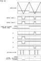
- Fig. 8 shows a first example of the method of controlling a power converter according to the embodiment.
- the duty ratio of the switching elements is controlled by using two carrier waves.
- gate signals Gu1 and Gu4 are generated by comparing a first carrier wave (solid line) that is a triangular wave with a reference signal for duty control.
- Gate signals Gu2 and Gu3 are generated by comparing a second carrier wave (broken line) derived from inverting the phase of the first carrier wave with a reference signal for duty control.
- the gate signals Gu1-Gu4 thus generated are shown in the second-fifth rows.
- the reference signal for duty control is adjusted in accordance with a voltage that the power converter 10 should output.
- the gate signals Gu1-Gu4 thus generated are supplied to the switching elements via the control lines.
- the switching patterns (2') and (3') are not used, and the switching patterns (2) and (3) are used. Therefore, the gate signal Gu1 is supplied to the switching elements S5a and S6a, the inverted version of the gate signal Gu1 is supplied to S7a and S8a, the gate signal Gu2 is supplied to S5b and S6b, the inverted version of the gate signal Gu2 is supplied to S7b and S8b , the gate signal Gu3 is supplied to the switching elements S5c and S6c, and the inverted version of the gate signal Gu3 is supplied to S7c and S8c, and the gate signal Gu4 is supplied to S5d and S6d, and the inverted version of the gate signal Gu4 is supplied to S7d and S8d.
- the switching pattern realized by the gate signals Gu1-Gu4 is shown in the sixth row, and the charge and discharge state of the flying capacitor is shown in the seventh row.
- the voltage across the flying capacitor can be maintained at a predetermined voltage by making it possible to adjust the duration of charge and the duration of discharge of the flying capacitor.
- the two carrier waves having inverted phases have the same level in the first period, but the level of the first carrier wave denoted by the solid line is adjusted to be lower in the second period.
- This causes the duration in which the gate signal Gu2 generated by the first carrier wave is at the high level to be longer than in the first period and causes the duration in which the gate signal Gu3 generated by the first carrier wave is at the low level to be longer than in the first period. Therefore, the duration in which the switching pattern (3) is induced is configured to be longer than the duration in which the second switching pattern (2) is induced. Therefore, the duration in which the flying capacitor is charged is longer than the duration in which the flying capacitor is discharged, with the result that the flying capacitor is charged and the voltage is increased.
- the switching patterns (2) and (3) may be used without using the switching patterns (2') and (3').
- using the switching patterns (2') and (3') in combination makes it possible to adjust the voltage across the flying capacitor on the U phase side and the voltage across the flying capacitor on the W phase side independently so that the variation in the voltage across the flying capacitor can be smoothed more finely and maintained at a predetermined level.
- the gate signals Gu1-Gu4 are inverted and supplied to the switching elements forming the third flying capacitor circuit 13 and the fourth flying capacitor circuit 14 on the W phase side.
- a first comparison circuit (not shown) that compares the voltage across the flying capacitor FC1 forming the first flying capacitor circuit 11 or the flying capacitor FC2 forming the second flying capacitor circuit 12 with a predetermined voltage
- a second comparison circuit (not shown) that compares the voltage across the flying capacitor FC3 forming the third flying capacitor circuit 13 or the flying capacitor FC4 forming the fourth flying capacitor circuit 14 with a predetermined voltage.
- the level of the carrier wave is adjusted so that the duration of charge of the flying capacitor FC3 or FC4 will be longer than the duration of discharge in the next and subsequent periods.
- the gate signals generated by the carrier wave having the adjusted level are supplied to switching elements forming the third flying capacitor circuit 13 and the fourth flying capacitor circuit 14.
- the level of the carrier wave is adjusted so that the duration of charge of the flying capacitor FC3 or FC4 will be shorter than the duration of discharge in the next and subsequent periods.
- the gate signals generated by the carrier wave having the adjusted level are supplied to switching elements forming the third flying capacitor circuit 13 and the fourth flying capacitor circuit 14.
- the voltage across the flying capacitor FC1 or FC3 forming the first flying capacitor circuit 11 or the third flying capacitor circuit 13 toward the top of the figure is compared with a predetermined voltage in the case the high-side switching elements S1a and S1b or the high-side switching elements S3a and S3b are turned on.
- the voltage across the flying capacitor FC2 or FC4 forming the second flying capacitor circuit 12 or the fourth flying capacitor circuit 14 toward the bottom of the figure is compared with a predetermined voltage in the case the low-side switching elements S2a and S2b or the low-side switching elements S4a and S4b are turned on. Accordingly, the flying capacitor is controlled to be charged or discharged based on the voltage across the flying capacitor located on the side where large current flows and changing heavily. Therefore, the voltages across the flying capacitors can be balanced more precisely and maintained at constant levels.
- comparison circuits for comparing the voltage of each of the flying capacitors FC1-FC4 with a predetermined voltage may be provided so that the voltage of each flying capacitor can be independently adjusted.
- a comparison circuit for comparing the voltage of one of the flying capacitors FC1-FC4 with a predetermined voltage may be provided so that the voltage of all flying capacitors may be adjusted based on the voltage of the one flying capacitor.
- Fig. 10 shows a third example of the method of controlling a power converter according to the embodiment.
- the duty ratio of the switching elements is controlled by using a single carrier wave.
- the carrier wave and the reference signal for duty control shown in the topmost row are used to generate a control signal A shown in the second row and a control signal B shown in the third row.
- the control signal B is an inverted version of the control signal A.
- a comparison circuit for comparing the voltage across the flying capacitor with a predetermined voltage is provided, and the output of the comparison circuit is used as a charge and discharge control signal shown in the fourth row. When the voltage across the flying capacitor is lower than the predetermined voltage, a high-level signal indicating charge is output in the next period. When the voltage across the flying capacitor is higher than the predetermined voltage, a low-level signal indicating discharge is output in the next period.
- One of the control signal A and the control signal B is allocated to the gate signals Gu1-Gu4 shown in the fifth-eighth rows, depending on the state of the charge and discharge control signal. More specifically, a gate signal that produces a switching pattern for charging the flying capacitor is generated when the charge and discharge signal has a high level indicating charge, and a gate signal that produces a switching pattern for discharging the flying capacitor is generated when the charge and discharge signal has a low level indicating discharge.
- the switching pattern realized by the gate signals Gu1-Gu4 is shown in the ninth row, and the charge and discharge state of the flying capacitor is shown in the tenth row.
- four comparison circuits for comparing the voltage of each of the flying capacitors FC1-FC4 with a predetermined voltage may be provided so that the voltage of each of the flying capacitors can be independently adjusted, or only a comparison circuit for comparing the voltage of one of the flying capacitors FC1-FC4 with a predetermined voltage may be provided so that the voltage of all flying capacitors is adjusted based on the voltage of the one flying capacitor.
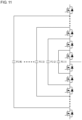
- Fig. 11 shows another example of the flying capacitor circuit of the power converter 10 according to the embodiment.
- the power converter 10 in which three-level flying capacitor circuits are used is described above. Flying capacitor circuits capable of outputting output voltages of more than three levels may be used as the first-fourth flying capacitor circuits of the power converter 10.
- one switching element is additionally connected in series with each of the high-potential side and the low-potential side of the four switching elements forming a one-stage flying capacitor circuit.
- a second flying capacitor FC(2) is further connected between the respective nodes between the additional two switching elements and the existing switching elements.
- an N-stage flying capacitor circuit (N is a natural number) is comprised of (2N+4) switching elements and N flying capacitors.
- the voltage across the first capacitor FC(1) is controlled to be (1/(2N+2)) times the DC power supply voltage E
- the voltage across the second capacitor FC(2) is controlled to be (2/(2N+2)) times the DC power supply voltage E
- the voltage across the N-th capacitor FC(N) is controlled to be (N/(2N+2)) times the voltage of the DC power supply voltage E.
- the N-stage flying capacitor circuit is capable of outputting (2N+1) levels of output voltage so that the power converter 10 comprised of four N-stage flying capacitor circuits is capable of outputting (2N+3) levels of voltage from the first output end OUT1 and the second output end OUT2.
- the present disclosure is applicable to power converters.
Landscapes
- Engineering & Computer Science (AREA)
- Power Engineering (AREA)
- Inverter Devices (AREA)
- Dc-Dc Converters (AREA)
Claims (8)
- Stromumwandlungsvorrichtung (10), aufweisend:eine erste Schwingkondensatorschaltung (11) und eine zweite Schwingkondensatorschaltung (12), die in Reihe verbunden sind, um parallel zu einer Gleichstromversorgung zu sein;eine dritte Schwingkondensatorschaltung (13) und eine vierte Schwingkondensatorschaltung (14), die in Reihe verbunden sind, um parallel zu der Gleichstromversorgung zu sein;ein erstes Schaltelement (S1) und ein zweites Schaltelement (S2), die in Reihe zwischen Ausgangsanschlüssen der ersten Schwingkondensatorschaltung (11) und der zweiten Schwingkondensatorschaltung (12) verbunden sind;ein drittes Schaltelement (S3) und ein viertes Schaltelement (S4), die in Reihe zwischen Ausgangsanschlüssen der dritten Schwingkondensatorschaltung (13) und der vierten Schwingkondensatorschaltung (14) verbunden sind;einen ersten Ausgangsanschluss (OUT1), der an einem Mittelpunkt zwischen dem ersten Schaltelement (S1) und dem zweiten Schaltelement (S2), die in Reihe verbunden sind, vorgesehen ist, undeinen zweiten Ausgangsanschluss (OUT2), der an einem Mittelpunkt zwischen dem dritten Schaltelement (S3) und dem vierten Schaltelement (S4) vorgesehen ist, die in Reihe verbunden sind, wobeiein Knoten zwischen der ersten Schwingkondensatorschaltung (11) und der zweiten Schwingkondensatorschaltung (12) und ein Knoten zwischen der dritten Schwingkondensatorschaltung (13) und der vierten Schwingkondensatorschaltung (14) mit einem Mittelpunkt einer Gleichstromversorgungsspannung verbunden sind unddie Stromumwandlungsvorrichtung so konfiguriert ist, dassvon dem ersten Ausgangsanschluss (OUT1) und dem zweiten Ausgangsanschluss (OUT2) einen Wechselstrom ausgeben wird,wobeidie erste Schwingkondensatorschaltung (11) aufweist:ein fünftes Schaltelement (S5a), ein sechstes Schaltelement (S5b), ein siebtes Schaltelement (S5c) und ein achtes Schaltelement, die in Reihe verbunden sind (S5d); undeinen ersten Kondensator (FC1), der zwischen einem Knoten des fünften Schaltelements (S5a) und dem sechsten Schaltelement (S5b) und einem Knoten des siebten Schaltelements (S5c) und dem achten Schaltelement (S5d) verbunden ist,wobei der Ausgangsanschluss der ersten Schwingkondensatorschaltung (11) zwischen dem sechsten Schaltelement (S5b) und dem siebten Schaltelement (S5c) vorgesehen ist,wobei die zweite Schwingkondensatorschaltung (12) aufweist:ein neuntes Schaltelement (S6a), ein zehntes Schaltelement (S6b), ein elftes Schaltelement (S6c) und ein zwölftes Schaltelement (S6d), die in Reihe verbunden sind; undeinen zweiten Kondensator (FC2), der zwischen einem Knoten des neunten Schaltelements und des zehnten Schaltelements und einem Knoten des elften Schaltelements und des zwölften Schaltelements verbunden ist,wobei der Ausgangsanschluss der zweiten Schwingkondensatorschaltung (12) zwischen dem zehnten Schaltelement (S6b) und dem elften Schaltelement (S6c) vorgesehen ist,wobei die dritte Schwingkondensatorschaltung (13) aufweist:ein dreizehntes Schaltelement (S7a), ein vierzehntes Schaltelement (S7b), ein fünfzehntes Schaltelement (S7c) und ein sechzehntes Schaltelement (S7d), die in Reihe verbunden sind; undeinen dritten Kondensator (FC3), der zwischen einem Knoten des dreizehnten Schaltelements (S7a) und des vierzehnten Schaltelements (S7b) und einem Knoten des fünfzehnten Schaltelements (S7c) und des sechzehnten Schaltelements (S7d) verbunden ist,wobei der Ausgangsanschluss der dritten Schwingkondensatorschaltung (13) zwischen dem vierzehnten Schaltelement (S7b) und dem fünfzehnten Schaltelement (S7c) vorgesehen ist,
unddie vierte Schwingkondensatorschaltung (14) aufweist:ein siebzehntes Schaltelement (S8a), ein achtzehntes Schaltelement (S8b), ein neunzehntes Schaltelement (S8c) und ein zwanzigstes Schaltelement (S8d), die in Reihe verbunden sind; undeinen vierten Kondensator (FC4), der zwischen einem Knoten des siebzehnten Schaltelements (S8a) und des achtzehnten Schaltelements (S8b) und einem Knoten des neunzehnten Schaltelements (S8c) und des zwanzigsten Schaltelements (S8d) verbunden ist,wobei der Ausgangsanschluss der vierten Schwingkondensatorschaltung (14) zwischen dem achtzehnten Schaltelement (S8b) und dem neunzehnten Schaltelement (S8c) vorgesehen ist,wobei eine Differenz zwischen einer Ausgangsspannung der ersten Schwingkondensatorschaltung (11) und einer Ausgangsspannung der zweiten Schwingkondensatorschaltung (12) und eine Differenz zwischen einer Ausgangsspannung der dritten Schwingkondensatorschaltung (13) und einer Ausgangsspannung der vierten Schwingkondensatorschaltung (14) so gesteuert werden, dass sie halb so groß wie die Gleichstromversorgungsspannung oder kleiner sind,das erste Schaltelement (S1), das zweite Schaltelement (S2), das dritte Schaltelement (S3) und das vierte Schaltelement (S4) so gesteuert werden, dass sie nur dann arbeiten, wenn eine Polarität des Wechselstroms, der von dem ersten Ausgangsanschluss (OUT1) und dem zweiten Ausgangsanschluss (OUT2) ausgegeben wird, umgeschaltet wird, undSchaltmuster von Schaltelementen, die die erste Schwingkondensatorschaltung (11), die zweite Schwingkondensatorschaltung (12), die dritte Schwingkondensatorschaltung (13) und die vierte Schwingkondensatorschaltung (14) bilden, die dazu angeregt werden, eine Spannung in Höhe der halben Gleichstromversorgungsspannung von dem ersten Ausgangsanschluss (OUT1) und dem zweiten Ausgangsanschluss (OUT2) auszugeben, ein erstes Schaltmuster, bei dem ein Schwingkondensator, der die erste Schwingkondensatorschaltung (11), die zweite Schwingkondensatorschaltung (12), die dritte Schwingkondensatorschaltung (13) oder die vierte Schwingkondensatorschaltung (14) bildet, aufgeladen wird, und ein zweites Schaltmuster, bei dem der Schwingkondensator entladen wird, aufweisen,wobei die Stromumwandlungsvorrichtung (10) ferner aufweist:eine erste Vergleichsschaltung und eine zweite Vergleichsschaltung, wobei die erste Vergleichsschaltung eine Spannung an einem Schwingkondensator, der die erste Schwingkondensatorschaltung (11) oder die zweite Schwingkondensatorschaltung (12) bildet, mit einer vorbestimmten Spannung vergleicht und die zweite Vergleichsschaltung eine Spannung an einem Schwingkondensator, der die dritte Schwingkondensatorschaltung (13) oder die vierte Schwingkondensatorschaltung (14) bildet, mit der vorbestimmten Spannung vergleicht, wobeiwenn die Spannung über dem Schwingkondensator, der die erste Schwingkondensatorschaltung (11) oder die zweite Schwingkondensatorschaltung (12) bildet, niedriger als die vorbestimmte Spannung ist, ein Steuersignal gleichermaßen an die Schaltelemente, die die erste Schwingkondensatorschaltung (11) und die zweite Schwingkondensatorschaltung (12) bilden, geliefert wird, so dass die Dauer, in der das erste Schaltmuster induziert wird, länger als die Dauer ist, in der das zweite Schaltmuster induziert wird, wenn die Spannung über dem Schwingkondensator, der die erste Schwingkondensatorschaltung (11) oder die zweite Schwingkondensatorschaltung (12) bildet, höher ist als die vorbestimmte Spannung, ein Steuersignal gleichermaßen an die Schaltelemente, die die erste Schwingkondensatorschaltung (11) und die zweite Schwingkondensatorschaltung (12) bilden, geliefert wird, so dass die Dauer, in der das erste Schaltmuster induziert wird, kürzer ist als die Dauer, in der das zweite Schaltmuster induziert wird,wenn die Spannung über dem Schwingkondensator, der die dritte Schwingkondensatorschaltung (13) oder die vierte Schwingkondensatorschaltung (14) bildet, niedriger ist als die vorbestimmte Spannung, ein Steuersignal gleichermaßen an die Schaltelemente, die die dritte Schwingkondensatorschaltung (13) und die vierte Schwingkondensatorschaltung (14) bilden, geliefert wird, so dass die Dauer, in der das erste Schaltmuster induziert wird, länger ist als die Dauer, in der das zweite Schaltmuster induziert wird, und wenn die Spannung über dem Schwingkondensator, der die dritte Schwingkondensatorschaltung (13) oder die vierte Schwingkondensatorschaltung (14) bildet, höher als die vorbestimmte Spannung ist, ein Steuersignal gleichermaßen an die Schaltelemente, die die dritte Schwingkondensatorschaltung (13) und die vierte Schwingkondensatorschaltung (14) bilden, geliefert wird, so dass die Dauer, in der das erste Schaltmuster induziert wird, kürzer als die Dauer ist, in der das zweite Schaltmuster induziert wird,wobeidie erste Vergleichsschaltung die Spannung über dem Schwingkondensator, der die Schwingkondensatorschaltung bildet, die mit einem Schaltelement verbunden ist, das eingeschaltet ist, mit der vorbestimmten Spannung vergleicht, wobei das Schaltelement eines von dem ersten Schaltelement (S1) und dem zweiten Schaltelement (S2) ist, unddie zweite Vergleichsschaltung die Spannung über dem Schwingkondensator, der die Schwingkondensatorschaltung bildet, die mit einem Schaltelement verbunden ist, das eingeschaltet ist, mit der vorbestimmten Spannung vergleicht, wobei das Schaltelement eines von dem dritten Schaltelement (S3) und dem vierten Schaltelement (S4) ist. - Stromumwandlungsvorrichtung (10) nach Anspruch 1, wobeieine Halbwelle des Wechselstroms erzeugt wird, während das erste Schaltelement (S1) und das vierte Schaltelement (S4) eingeschaltet sind und das zweite Schaltelement (S2) und das dritte Schaltelement (S3) ausgeschaltet sind, undeine Halbwelle des Wechselstroms mit entgegengesetzter Polarität erzeugt wird, während das erste Schaltelement (S1) und das vierte Schaltelement (S4) ausgeschaltet sind und das zweite Schaltelement (S2) und das dritte Schaltelement (S3) eingeschaltet sind.
- Stromumwandlungsvorrichtung (10) nach Anspruch 1 oder 2, wobei
ein Umschalten zwischen einem Zustand, in dem das erste Schaltelement (S1) und das vierte Schaltelement (S4) eingeschaltet sind und das zweite Schaltelement (S2) und das dritte Schaltelement (S3) ausgeschaltet sind, und einem Zustand, in dem das erste Schaltelement (S1) und das vierte Schaltelement (S4) ausgeschaltet sind und das zweite Schaltelement (S2) und das dritte Schaltelement (S3) eingeschaltet sind, so gesteuert wird, dass es erfolgt, wenn eine Polarität des Wechselstrom, der von dem ersten Ausgangsanschluss (OUT1) und dem zweiten Ausgangsanschluss (OUT2) ausgegeben wird, umgeschaltet wird. - Stromumwandlungsvorrichtung (10) nach einem der Ansprüche 1 bis 3, wobei
mehrere Schaltelemente mit einer niedrigeren Spannungsfestigkeit als das erste Schaltelement (S1), das zweite Schaltelement (S2), das dritte Schaltelement (S3) oder das vierte Schaltelement (S4) anstelle des ersten Schaltelements (S1), des zweiten Schaltelements (S2), des dritten Schaltelements (S3) oder des vierten Schaltelements (S4) in Reihe verbunden sind. - Stromumwandlungsvorrichtung (10) nach einem der Ansprüche 1 bis 4, wobeidie erste Schwingkondensatorschaltung (11) einen Kondensator aufweist,die zweite Schwingkondensatorschaltung (12) einen Kondensator aufweist,die dritte Schwingkondensatorschaltung (13) einen Kondensator aufweist,die vierte Schwingkondensatorschaltung (14) einen Kondensator aufweist,eine Spannung über dem einen Kondensator so gesteuert wird, dass sie 1/4 der Gleichstromversorgungsspannung beträgt, undfünf Spannungspegel von dem ersten Ausgangsanschluss (OUT1) und dem zweiten Ausgangsanschluss (OUT2) ausgegeben werden.
- Stromumwandlungsvorrichtung (10) nach einem der Ansprüche 1 bis 4, wobeidie erste Schwingkondensatorschaltung (11) N Kondensatoren aufweist (wobei N eine natürliche Zahl ist),die zweite Schwingkondensatorschaltung (12) N Kondensatoren aufweist (wobei N eine natürliche Zahl ist),die dritte Schwingkondensatorschaltung (13) N Kondensatoren aufweist (wobei N eine natürliche Zahl ist),die vierte Schwingkondensatorschaltung (14) N Kondensatoren aufweist (wobei N eine natürliche Zahl ist),eine Spannung über einem ersten Kondensator so gesteuert wird, dass sie das (1/(2N+2))-fache der Gleichstromversorgungsspannung beträgt,eine Spannung an einem zweiten Kondensator so gesteuert wird, dass sie das (2/(2N+2))-fache der Gleichstromversorgungsspannung beträgt,eine Spannung an einem N-ten Kondensator so gesteuert wird, dass sie das (N/(2N+2))-fache der Gleichstromversorgungsspannung beträgt, und(2N+3) Spannungspegel von dem ersten Ausgangsanschluss (OUT1) und dem zweiten Ausgangsanschluss (OUT2) ausgegeben werden.
- Stromumwandlungsvorrichtung (10) nach einem der Ansprüche 1 bis 6, wobei
für Schaltelemente der ersten Schwingkondensatorschaltung (11), Schaltelemente der zweiten Schwingkondensatorschaltung (12), Schaltelemente der dritten Schwingkondensatorschaltung (13) und Schaltelemente der vierten Schwingkondensatorschaltung (14) Elemente mit einer Spannungsfestigkeit verwendet werden, die niedriger ist als die Gleichstromversorgungsspannung. - Stromumwandlungsvorrichtung (10) nach einem der Ansprüche 1 bis 7,
wobei für das erste Schaltelement (S1), das zweite Schaltelement (S2), das dritte Schaltelement (S3) oder das vierte Schaltelement (S4) ein Element mit einer Spannungsfestigkeit verwendet wird, die niedriger ist als die Gleichstromversorgungsspannung.
Applications Claiming Priority (3)
| Application Number | Priority Date | Filing Date | Title |
|---|---|---|---|
| JP2017195668 | 2017-10-06 | ||
| JP2017195667 | 2017-10-06 | ||
| PCT/JP2018/034026 WO2019069654A1 (ja) | 2017-10-06 | 2018-09-13 | 電力変換装置 |
Publications (3)
| Publication Number | Publication Date |
|---|---|
| EP3694095A1 EP3694095A1 (de) | 2020-08-12 |
| EP3694095A4 EP3694095A4 (de) | 2020-12-09 |
| EP3694095B1 true EP3694095B1 (de) | 2025-07-09 |
Family
ID=65994949
Family Applications (1)
| Application Number | Title | Priority Date | Filing Date |
|---|---|---|---|
| EP18865083.2A Active EP3694095B1 (de) | 2017-10-06 | 2018-09-13 | Stromumwandlungsvorrichtung |
Country Status (7)
| Country | Link |
|---|---|
| US (1) | US11451163B2 (de) |
| EP (1) | EP3694095B1 (de) |
| JP (1) | JPWO2019069654A1 (de) |
| CN (1) | CN111164877B (de) |
| AU (1) | AU2018344692B2 (de) |
| NZ (1) | NZ763075A (de) |
| WO (1) | WO2019069654A1 (de) |
Families Citing this family (13)
| Publication number | Priority date | Publication date | Assignee | Title |
|---|---|---|---|---|
| JPWO2019069654A1 (ja) * | 2017-10-06 | 2020-06-18 | パナソニックIpマネジメント株式会社 | 電力変換装置 |
| US12003190B2 (en) * | 2019-03-09 | 2024-06-04 | Cornell University | Switched energy buffering |
| EP3939156A4 (de) * | 2019-03-11 | 2022-11-23 | Versitech Limited | Gleichstrom- und gleichstromwandler |
| JP7186378B2 (ja) * | 2019-04-15 | 2022-12-09 | パナソニックIpマネジメント株式会社 | 電力変換装置 |
| JP7153878B2 (ja) * | 2019-05-21 | 2022-10-17 | パナソニックIpマネジメント株式会社 | 電力変換装置 |
| JP7262049B2 (ja) * | 2019-06-28 | 2023-04-21 | パナソニックIpマネジメント株式会社 | 電力変換装置 |
| JP7270139B2 (ja) | 2019-08-21 | 2023-05-10 | パナソニックIpマネジメント株式会社 | Dc/dc変換装置 |
| CN112737387A (zh) * | 2019-10-14 | 2021-04-30 | 台达电子工业股份有限公司 | 电力系统 |
| EP3846329B1 (de) * | 2019-12-31 | 2025-08-06 | Solaredge Technologies Ltd. | Gleichstromausgleichsschaltung mit zvs |
| US11567519B2 (en) | 2020-09-08 | 2023-01-31 | Samsung Electronics Co., Ltd. | Voltage dividing capacitor circuits, supply modulators and wireless communication devices |
| CN112910230B (zh) * | 2021-03-01 | 2025-06-10 | 江苏师范大学 | 一种简化的五电平电压源型变换装置 |
| US11936291B2 (en) * | 2021-11-08 | 2024-03-19 | Psemi Corporation | Controlling charge-balance and transients in a multi-level power converter |
| JP2023141632A (ja) * | 2022-03-24 | 2023-10-05 | 東芝インフラシステムズ株式会社 | 電力変換装置 |
Citations (7)
| Publication number | Priority date | Publication date | Assignee | Title |
|---|---|---|---|---|
| EP1901419B1 (de) * | 2003-06-09 | 2009-03-11 | Kyosemi Corporation | Generatorsystem |
| US20090152950A1 (en) * | 2005-01-08 | 2009-06-18 | Emerson Network Power Energy Systems Ab | Switching Power Supply With Overvoltage Protection And Overvoltage Protection Method Thereof |
| EP2461468A1 (de) * | 2010-12-06 | 2012-06-06 | Samsung Electronics Co., Ltd. | Stromversorgungsvorrichtung und Verfahren zu ihrer Regelung |
| DE102012203995A1 (de) * | 2011-03-15 | 2012-09-20 | Infineon Technologies Ag | Verfahren zum Steuern eines Stromes zwischen einer Quelle und einer Last und Schaltmodul |
| US20130181532A1 (en) * | 2010-05-27 | 2013-07-18 | Vestas Wind Systems A/S | High-voltage power converter |
| US20170070047A1 (en) * | 2014-05-09 | 2017-03-09 | Nr Electric Co., Ltd | Voltage-source multi-level converter, dc power transmission system, and fault processing method and device |
| US9780658B2 (en) * | 2014-09-30 | 2017-10-03 | Siemens Aktiengesellschaft | Intermediate voltage circuit current converter in five-point topology |
Family Cites Families (16)
| Publication number | Priority date | Publication date | Assignee | Title |
|---|---|---|---|---|
| JPS52137931A (en) | 1976-05-13 | 1977-11-17 | Sharp Corp | Input output device |
| US20090033293A1 (en) * | 2007-08-01 | 2009-02-05 | Intersil Americas Inc. | Voltage converter with combined capacitive voltage divider, buck converter and battery charger |
| JP2012080753A (ja) * | 2010-05-11 | 2012-04-19 | Meidensha Corp | 電力変換装置 |
| JP6040582B2 (ja) * | 2012-06-14 | 2016-12-07 | 富士電機株式会社 | マルチレベル電力変換回路の保護制御方式 |
| JP5626293B2 (ja) | 2012-08-29 | 2014-11-19 | 株式会社村田製作所 | インバータ装置 |
| JP6025128B2 (ja) * | 2012-09-13 | 2016-11-16 | 国立研究開発法人産業技術総合研究所 | マルチレベル電力変換回路および装置 |
| JP6079407B2 (ja) * | 2013-04-22 | 2017-02-15 | 富士電機株式会社 | マルチレベル変換回路 |
| JP6146130B2 (ja) * | 2013-05-21 | 2017-06-14 | 富士電機株式会社 | 電力変換装置のゲート駆動電源供給回路 |
| JP6206118B2 (ja) * | 2013-08-02 | 2017-10-04 | 株式会社明電舎 | マルチレベル電力変換装置 |
| JP6232944B2 (ja) * | 2013-11-06 | 2017-11-22 | 株式会社明電舎 | マルチレベル電力変換装置 |
| JP6191965B2 (ja) * | 2014-05-12 | 2017-09-06 | パナソニックIpマネジメント株式会社 | 電力変換装置、およびそれを用いたパワーコンディショナ |
| JPWO2019069654A1 (ja) * | 2017-10-06 | 2020-06-18 | パナソニックIpマネジメント株式会社 | 電力変換装置 |
| CH715448A2 (de) * | 2018-10-15 | 2020-04-15 | Prodrive Tech Bv | Mehrphasige Umrichtertopologie für mehrphasigen und einphasigen Betrieb. |
| WO2021074661A1 (en) * | 2019-10-16 | 2021-04-22 | ZHU, Karen Ming | Multibridge power converter with multiple outputs |
| JP7439671B2 (ja) * | 2020-07-15 | 2024-02-28 | Tdk株式会社 | スイッチング電源装置および電力供給システム |
| MX2023003586A (es) * | 2020-09-28 | 2023-06-20 | Tae Tech Inc | Marcos de sistemas de energía multifásicos basados en módulos y métodos relacionados con ellos. |
-
2018
- 2018-09-13 JP JP2019546605A patent/JPWO2019069654A1/ja active Pending
- 2018-09-13 EP EP18865083.2A patent/EP3694095B1/de active Active
- 2018-09-13 AU AU2018344692A patent/AU2018344692B2/en active Active
- 2018-09-13 US US16/753,475 patent/US11451163B2/en active Active
- 2018-09-13 NZ NZ763075A patent/NZ763075A/en unknown
- 2018-09-13 WO PCT/JP2018/034026 patent/WO2019069654A1/ja not_active Ceased
- 2018-09-13 CN CN201880064250.8A patent/CN111164877B/zh active Active
Patent Citations (7)
| Publication number | Priority date | Publication date | Assignee | Title |
|---|---|---|---|---|
| EP1901419B1 (de) * | 2003-06-09 | 2009-03-11 | Kyosemi Corporation | Generatorsystem |
| US20090152950A1 (en) * | 2005-01-08 | 2009-06-18 | Emerson Network Power Energy Systems Ab | Switching Power Supply With Overvoltage Protection And Overvoltage Protection Method Thereof |
| US20130181532A1 (en) * | 2010-05-27 | 2013-07-18 | Vestas Wind Systems A/S | High-voltage power converter |
| EP2461468A1 (de) * | 2010-12-06 | 2012-06-06 | Samsung Electronics Co., Ltd. | Stromversorgungsvorrichtung und Verfahren zu ihrer Regelung |
| DE102012203995A1 (de) * | 2011-03-15 | 2012-09-20 | Infineon Technologies Ag | Verfahren zum Steuern eines Stromes zwischen einer Quelle und einer Last und Schaltmodul |
| US20170070047A1 (en) * | 2014-05-09 | 2017-03-09 | Nr Electric Co., Ltd | Voltage-source multi-level converter, dc power transmission system, and fault processing method and device |
| US9780658B2 (en) * | 2014-09-30 | 2017-10-03 | Siemens Aktiengesellschaft | Intermediate voltage circuit current converter in five-point topology |
Non-Patent Citations (1)
| Title |
|---|
| RODRIGUEZ J ET AL: "Multilevel Converters: An Enabling Technology for High-Power Applications", PROCEEDINGS OF THE IEEE, IEEE. NEW YORK, US, vol. 97, no. 11, 1 November 2009 (2009-11-01), pages 1786 - 1817, XP011278598, ISSN: 0018-9219, DOI: 10.1109/JPROC.2009.2030235 * |
Also Published As
| Publication number | Publication date |
|---|---|
| CN111164877A (zh) | 2020-05-15 |
| NZ763075A (en) | 2022-02-25 |
| EP3694095A4 (de) | 2020-12-09 |
| US20210367532A1 (en) | 2021-11-25 |
| WO2019069654A1 (ja) | 2019-04-11 |
| JPWO2019069654A1 (ja) | 2020-06-18 |
| AU2018344692A1 (en) | 2020-04-16 |
| AU2018344692B2 (en) | 2021-05-20 |
| EP3694095A1 (de) | 2020-08-12 |
| US11451163B2 (en) | 2022-09-20 |
| CN111164877B (zh) | 2024-01-30 |
Similar Documents
| Publication | Publication Date | Title |
|---|---|---|
| EP3694095B1 (de) | Stromumwandlungsvorrichtung | |
| US10541623B1 (en) | Circuit with an input voltage divider and two half-bridges | |
| EP3301804B1 (de) | Umrichter, verfahren und vorrichtung zur steuerung davon | |
| Nami et al. | Five level cross connected cell for cascaded converters | |
| US9748862B2 (en) | Sparse matrix multilevel actively clamped power converter | |
| US20160268924A1 (en) | Multi-Level Inverter Apparatus and Method | |
| US11239765B2 (en) | Multi-level circuit, three-phase multi-level circuit, and control method | |
| EP2924860A1 (de) | Spannungsquellenwandler und Steuerung dafür | |
| EP4007144A1 (de) | Gleichspannungswandlungsvorrichtung | |
| US20180309383A1 (en) | Five-Level Inverter Topology with High Voltage Utilization Ratio | |
| ES2754716T3 (es) | Circuito de prueba sintético para una prueba de rendimiento de válvula de HVDC | |
| US20160064160A1 (en) | 4-Switch Extended Commutation Cell | |
| EP2897278B1 (de) | Stromumwandlungssystem und -verfahren | |
| EP2961057A1 (de) | Spannungsquellenwandler und Steuerung dafür | |
| WO2017157271A1 (en) | Multilevel inverters | |
| EP3633843B1 (de) | Stromwandler und ansteuerverfahren dafür | |
| JP2014135799A (ja) | 電力変換装置 | |
| JP5362657B2 (ja) | 電力変換装置 | |
| RU2269196C1 (ru) | Преобразователь напряжения, выполненный по комбинированной схеме | |
| JP7165923B2 (ja) | 電力変換装置 | |
| CN114553038B (zh) | 一种空间型dc/ac变换器及其容错运行方法 | |
| CN214544144U (zh) | 一种三电平逆变器的pwm驱动保护装置 | |
| JP2020054058A (ja) | 半導体装置及びデバイス | |
| Mouselinos et al. | Multilevel inverters: A survey of limitations and recommended problem-solving techniques | |
| Tekwani et al. | Analysis of carrier offset technique used in a five-level inverter scheme with emphasis on dc-link capacitor voltage balancing |
Legal Events
| Date | Code | Title | Description |
|---|---|---|---|
| STAA | Information on the status of an ep patent application or granted ep patent |
Free format text: STATUS: THE INTERNATIONAL PUBLICATION HAS BEEN MADE |
|
| PUAI | Public reference made under article 153(3) epc to a published international application that has entered the european phase |
Free format text: ORIGINAL CODE: 0009012 |
|
| STAA | Information on the status of an ep patent application or granted ep patent |
Free format text: STATUS: REQUEST FOR EXAMINATION WAS MADE |
|
| 17P | Request for examination filed |
Effective date: 20200428 |
|
| AK | Designated contracting states |
Kind code of ref document: A1 Designated state(s): AL AT BE BG CH CY CZ DE DK EE ES FI FR GB GR HR HU IE IS IT LI LT LU LV MC MK MT NL NO PL PT RO RS SE SI SK SM TR |
|
| AX | Request for extension of the european patent |
Extension state: BA ME |
|
| A4 | Supplementary search report drawn up and despatched |
Effective date: 20201106 |
|
| RIC1 | Information provided on ipc code assigned before grant |
Ipc: H02M 7/487 20070101AFI20201102BHEP Ipc: H02M 7/483 20070101ALI20201102BHEP Ipc: H02M 7/48 20070101ALI20201102BHEP |
|
| DAV | Request for validation of the european patent (deleted) | ||
| DAX | Request for extension of the european patent (deleted) | ||
| STAA | Information on the status of an ep patent application or granted ep patent |
Free format text: STATUS: EXAMINATION IS IN PROGRESS |
|
| 17Q | First examination report despatched |
Effective date: 20220607 |
|
| GRAP | Despatch of communication of intention to grant a patent |
Free format text: ORIGINAL CODE: EPIDOSNIGR1 |
|
| STAA | Information on the status of an ep patent application or granted ep patent |
Free format text: STATUS: GRANT OF PATENT IS INTENDED |
|
| INTG | Intention to grant announced |
Effective date: 20250212 |
|
| GRAS | Grant fee paid |
Free format text: ORIGINAL CODE: EPIDOSNIGR3 |
|
| GRAA | (expected) grant |
Free format text: ORIGINAL CODE: 0009210 |
|
| STAA | Information on the status of an ep patent application or granted ep patent |
Free format text: STATUS: THE PATENT HAS BEEN GRANTED |
|
| AK | Designated contracting states |
Kind code of ref document: B1 Designated state(s): AL AT BE BG CH CY CZ DE DK EE ES FI FR GB GR HR HU IE IS IT LI LT LU LV MC MK MT NL NO PL PT RO RS SE SI SK SM TR |
|
| REG | Reference to a national code |
Ref country code: GB Ref legal event code: FG4D |
|
| REG | Reference to a national code |
Ref country code: CH Ref legal event code: EP |
|
| REG | Reference to a national code |
Ref country code: IE Ref legal event code: FG4D |
|
| REG | Reference to a national code |
Ref country code: DE Ref legal event code: R096 Ref document number: 602018083488 Country of ref document: DE |
|
| PGFP | Annual fee paid to national office [announced via postgrant information from national office to epo] |
Ref country code: DE Payment date: 20250919 Year of fee payment: 8 |
|
| REG | Reference to a national code |
Ref country code: NL Ref legal event code: MP Effective date: 20250709 |
|
| PG25 | Lapsed in a contracting state [announced via postgrant information from national office to epo] |
Ref country code: PT Free format text: LAPSE BECAUSE OF FAILURE TO SUBMIT A TRANSLATION OF THE DESCRIPTION OR TO PAY THE FEE WITHIN THE PRESCRIBED TIME-LIMIT Effective date: 20251110 |
|
| PG25 | Lapsed in a contracting state [announced via postgrant information from national office to epo] |
Ref country code: NL Free format text: LAPSE BECAUSE OF FAILURE TO SUBMIT A TRANSLATION OF THE DESCRIPTION OR TO PAY THE FEE WITHIN THE PRESCRIBED TIME-LIMIT Effective date: 20250709 |
|
| REG | Reference to a national code |
Ref country code: AT Ref legal event code: MK05 Ref document number: 1812829 Country of ref document: AT Kind code of ref document: T Effective date: 20250709 |
|
| PG25 | Lapsed in a contracting state [announced via postgrant information from national office to epo] |
Ref country code: IS Free format text: LAPSE BECAUSE OF FAILURE TO SUBMIT A TRANSLATION OF THE DESCRIPTION OR TO PAY THE FEE WITHIN THE PRESCRIBED TIME-LIMIT Effective date: 20251109 |
|
| PG25 | Lapsed in a contracting state [announced via postgrant information from national office to epo] |
Ref country code: NO Free format text: LAPSE BECAUSE OF FAILURE TO SUBMIT A TRANSLATION OF THE DESCRIPTION OR TO PAY THE FEE WITHIN THE PRESCRIBED TIME-LIMIT Effective date: 20251009 |
|
| REG | Reference to a national code |
Ref country code: LT Ref legal event code: MG9D |
|
| PG25 | Lapsed in a contracting state [announced via postgrant information from national office to epo] |
Ref country code: AT Free format text: LAPSE BECAUSE OF FAILURE TO SUBMIT A TRANSLATION OF THE DESCRIPTION OR TO PAY THE FEE WITHIN THE PRESCRIBED TIME-LIMIT Effective date: 20250709 |
|
| PG25 | Lapsed in a contracting state [announced via postgrant information from national office to epo] |
Ref country code: FI Free format text: LAPSE BECAUSE OF FAILURE TO SUBMIT A TRANSLATION OF THE DESCRIPTION OR TO PAY THE FEE WITHIN THE PRESCRIBED TIME-LIMIT Effective date: 20250709 |
|
| PG25 | Lapsed in a contracting state [announced via postgrant information from national office to epo] |
Ref country code: HR Free format text: LAPSE BECAUSE OF FAILURE TO SUBMIT A TRANSLATION OF THE DESCRIPTION OR TO PAY THE FEE WITHIN THE PRESCRIBED TIME-LIMIT Effective date: 20250709 |
|
| PG25 | Lapsed in a contracting state [announced via postgrant information from national office to epo] |
Ref country code: GR Free format text: LAPSE BECAUSE OF FAILURE TO SUBMIT A TRANSLATION OF THE DESCRIPTION OR TO PAY THE FEE WITHIN THE PRESCRIBED TIME-LIMIT Effective date: 20251010 |
|
| PG25 | Lapsed in a contracting state [announced via postgrant information from national office to epo] |
Ref country code: SE Free format text: LAPSE BECAUSE OF FAILURE TO SUBMIT A TRANSLATION OF THE DESCRIPTION OR TO PAY THE FEE WITHIN THE PRESCRIBED TIME-LIMIT Effective date: 20250709 |
|
| PG25 | Lapsed in a contracting state [announced via postgrant information from national office to epo] |
Ref country code: LV Free format text: LAPSE BECAUSE OF FAILURE TO SUBMIT A TRANSLATION OF THE DESCRIPTION OR TO PAY THE FEE WITHIN THE PRESCRIBED TIME-LIMIT Effective date: 20250709 |
|
| PG25 | Lapsed in a contracting state [announced via postgrant information from national office to epo] |
Ref country code: BG Free format text: LAPSE BECAUSE OF FAILURE TO SUBMIT A TRANSLATION OF THE DESCRIPTION OR TO PAY THE FEE WITHIN THE PRESCRIBED TIME-LIMIT Effective date: 20250709 Ref country code: PL Free format text: LAPSE BECAUSE OF FAILURE TO SUBMIT A TRANSLATION OF THE DESCRIPTION OR TO PAY THE FEE WITHIN THE PRESCRIBED TIME-LIMIT Effective date: 20250709 |
|
| PG25 | Lapsed in a contracting state [announced via postgrant information from national office to epo] |
Ref country code: RS Free format text: LAPSE BECAUSE OF FAILURE TO SUBMIT A TRANSLATION OF THE DESCRIPTION OR TO PAY THE FEE WITHIN THE PRESCRIBED TIME-LIMIT Effective date: 20251009 |
|
| PG25 | Lapsed in a contracting state [announced via postgrant information from national office to epo] |
Ref country code: ES Free format text: LAPSE BECAUSE OF FAILURE TO SUBMIT A TRANSLATION OF THE DESCRIPTION OR TO PAY THE FEE WITHIN THE PRESCRIBED TIME-LIMIT Effective date: 20250709 |