EP3690389A1 - Strain gauge - Google Patents
Strain gauge Download PDFInfo
- Publication number
- EP3690389A1 EP3690389A1 EP18863695.5A EP18863695A EP3690389A1 EP 3690389 A1 EP3690389 A1 EP 3690389A1 EP 18863695 A EP18863695 A EP 18863695A EP 3690389 A1 EP3690389 A1 EP 3690389A1
- Authority
- EP
- European Patent Office
- Prior art keywords
- metallic layer
- resistor
- layer
- strain gauge
- gauge according
- Prior art date
- Legal status (The legal status is an assumption and is not a legal conclusion. Google has not performed a legal analysis and makes no representation as to the accuracy of the status listed.)
- Pending
Links
Images


Classifications
-
- H—ELECTRICITY
- H01—ELECTRIC ELEMENTS
- H01C—RESISTORS
- H01C7/00—Non-adjustable resistors formed as one or more layers or coatings; Non-adjustable resistors made from powdered conducting material or powdered semi-conducting material with or without insulating material
- H01C7/006—Thin film resistors
-
- G—PHYSICS
- G01—MEASURING; TESTING
- G01L—MEASURING FORCE, STRESS, TORQUE, WORK, MECHANICAL POWER, MECHANICAL EFFICIENCY, OR FLUID PRESSURE
- G01L1/00—Measuring force or stress, in general
- G01L1/20—Measuring force or stress, in general by measuring variations in ohmic resistance of solid materials or of electrically-conductive fluids; by making use of electrokinetic cells, i.e. liquid-containing cells wherein an electrical potential is produced or varied upon the application of stress
- G01L1/22—Measuring force or stress, in general by measuring variations in ohmic resistance of solid materials or of electrically-conductive fluids; by making use of electrokinetic cells, i.e. liquid-containing cells wherein an electrical potential is produced or varied upon the application of stress using resistance strain gauges
- G01L1/2287—Measuring force or stress, in general by measuring variations in ohmic resistance of solid materials or of electrically-conductive fluids; by making use of electrokinetic cells, i.e. liquid-containing cells wherein an electrical potential is produced or varied upon the application of stress using resistance strain gauges constructional details of the strain gauges
-
- G—PHYSICS
- G01—MEASURING; TESTING
- G01B—MEASURING LENGTH, THICKNESS OR SIMILAR LINEAR DIMENSIONS; MEASURING ANGLES; MEASURING AREAS; MEASURING IRREGULARITIES OF SURFACES OR CONTOURS
- G01B7/00—Measuring arrangements characterised by the use of electric or magnetic techniques
- G01B7/16—Measuring arrangements characterised by the use of electric or magnetic techniques for measuring the deformation in a solid, e.g. by resistance strain gauge
-
- G—PHYSICS
- G01—MEASURING; TESTING
- G01B—MEASURING LENGTH, THICKNESS OR SIMILAR LINEAR DIMENSIONS; MEASURING ANGLES; MEASURING AREAS; MEASURING IRREGULARITIES OF SURFACES OR CONTOURS
- G01B7/00—Measuring arrangements characterised by the use of electric or magnetic techniques
- G01B7/16—Measuring arrangements characterised by the use of electric or magnetic techniques for measuring the deformation in a solid, e.g. by resistance strain gauge
- G01B7/18—Measuring arrangements characterised by the use of electric or magnetic techniques for measuring the deformation in a solid, e.g. by resistance strain gauge using change in resistance
-
- H—ELECTRICITY
- H01—ELECTRIC ELEMENTS
- H01C—RESISTORS
- H01C1/00—Details
- H01C1/14—Terminals or tapping points specially adapted for resistors; Arrangements of terminals or tapping points on resistors
Definitions
- the present invention relates to a strain gauge.
- a strain gauge is known to be attached to a measured object to detect strain on the measured object.
- the strain gauge includes a resistor that detects strain, and as resistor material, for example, material including Cr (chromium) or Ni (nickel) is used.
- resistor material for example, material including Cr (chromium) or Ni (nickel) is used.
- resistor material for example, material including Cr (chromium) or Ni (nickel) is used.
- resistor material for example, material including Cr (chromium) or Ni (nickel) is used.
- resistor material for example, material including Cr (chromium) or Ni (nickel) is used.
- both ends of the resistor are used as electrodes, and a lead wire for an external connection, or the like is jointed with solder, between the electrodes (see, for example, Patent document 1).
- Patent document 1 Japanese Unexamined Patent Application Publication No. 2016-74934
- a resistor has a thin film thickness and when both ends of the resistor are used as electrodes, dissolution of metallization easily occurs, which results in less solderability. Further, when material including Cr (chromium) or Ni (nickel) is used for the resistor, solderability further gets worse. Particularly, Cr forms an autoxidized film and thus solderability gets worse.
- an object of the present invention is to improve solderability of an electrode with respect to a strain gauge in which material including Cr (chromium) or Ni (nickel) is used for a resistor.
- a strain gauge includes a flexible substrate; a resistor formed of material including at least one from among chromium and nickel, on or above the substrate; and electrodes electrically coupled to the resistor.
- Each electrode includes a terminal section extending from a corresponding end portion from among end portions of the resistor; a first metallic layer formed of copper, a copper alloy, nickel, or a nickel alloy, on or above the terminal section; and a second metallic layer formed of material having better solder wettability than the first metallic layer, on or above the first metallic layer.
- solderability of an electrode can be improved.
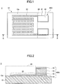
- Fig. 1 is a plan view of an example of a strain gauge according to a first embodiment.
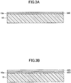
- Fig. 2 is a cross-sectional view of an example of the strain gauge according to the first embodiment, and illustrates a cross section taken along the A-A line in Fig. 1 .
- the strain gauge 1 includes a substrate 10, a resistor 30, and electrodes 40A.
- the side of the substrate 10 where the resistor 30 is provided is referred to as an upper side or one side; and the side of the substrate 10 where the resistor 30 is not provided is referred to as a lower side or another side.
- the surface on the side where the resistor 30 is provided is referred to as one surface or an upper surface; and the surface on the side where the resistor 30 is not provided is referred to as another surface or a lower surface.
- the strain gauge 1 can be used in a state of being upside down, or be disposed at any angle.
- a plan view means that an object is viewed from a normal direction of an upper surface 10a of the substrate 10, and a planar shape refers to a shape of an object when viewed from the normal direction of the upper surface 10a of the substrate 10.
- the substrate 10 is a member that is a base layer for forming the resistor 30 or the like and is flexible.
- the thickness of the substrate 10 is not particularly restricted, and can be appropriately selected for any purpose. For example, such a thickness can be approximately between 5 ⁇ m and 500 ⁇ m. In particular, when the thickness of the substrate 10 is between 5 ⁇ m and 200 ⁇ m, it is preferable in terms of strain transfer from a flexure element surface that is bonded to a lower surface of the substrate 10 via an adhesive layer or the like; and dimensional stability with respect to environment, and when the thickness is 10 ⁇ m or more, it is further preferable in terms of insulation.
- the substrate 10 can be formed of an insulating resin film such as a PI (polyimide) resin, an epoxy resin, a PEEK (polyether ether ketone) resin, a PEN (polyethylene naphthalate) resin, a PET (polyethylene terephthalate) resin, a PPS (polyphenylene sulfide) resin, or a polyolefin resin.
- PI polyimide
- PEEK polyether ether ketone
- PEN polyethylene naphthalate
- PET polyethylene terephthalate
- PPS polyphenylene sulfide
- the "formed of an insulating resin film” is not intended to preclude the substrate 10 from containing fillers, impurities, or the like in the insulating resin film.
- the substrate 10 may be formed of, for example, an insulating resin film containing fillers such as silica or alumina.
- the resistor 30 is a thin film formed in a predetermined pattern and is a sensitive section where resistance varies according to strain.
- the resistor 30 may be formed directly on the upper surface 10a of the substrate 10, or be formed above the upper surface 10a of the substrate 10, via other layer(s). Note that in Fig. 1 , for the sake of convenience, the resistor 30 is illustrated in a crepe pattern.
- the resistor 30 can be formed of, for example, material including Cr (chromium); material including Ni (nickel); or material including both of Cr and Ni. In other words, the resistor 30 can be formed of material including at least one from among Cr and Ni.
- An example of the material including Cr includes a Cr composite film.
- An example of the material including nickel includes Cu-Ni (copper nickel).
- An example of the material including both of Cr and Ni includes Ni-Cr (nickel chromium).
- the Cr composite film is a composite film of Cr, CrN, Cr 2 N, and the like.
- the Cr composite film may include incidental impurities such as chromium oxide.
- the thickness of the resistor 30 is not particularly restricted, and can be appropriately selected for any purpose.
- the thickness can be, for example, approximately between 0.05 ⁇ m and 2 ⁇ m.
- the resistor 30 when the resistor 30 is the Cr composite film, the resistor is formed with ⁇ -Cr (alpha-chromium) as the main component having a stable crystalline phase, so that stability of the gauge characteristics can be improved.
- the gauge factor of the strain gauge 1 when the resistor 30 is formed with ⁇ -Cr as the main component, can be 10 or more, as well as a gauge factor temperature coefficient TCS and temperature coefficient of resistance TCR can be each in the range of from -1000 ppm/°C to +1000 ppm/°C.
- a main component means that a target substance has 50% by weight or more of total substances that constitute the resistor.
- the resistor 30 preferably includes ⁇ -Cr of 80% by weight or more, from the viewpoint of improving the gauge characteristics. Note that ⁇ -Cr is Cr having a bcc structure (body-centered cubic structure).
- the electrodes 40A respectively extend from both end portions of the resistor 30 and are each wider than the resistor 30 to be in an approximately rectangular shape, in a plan view.
- the electrodes 40A are a pair of electrodes from which a change in a resistance value of the resistor 30 according to strain is output externally, where, for example, a lead wire for an external connection, or the like is joined.
- the resistor 30 extends zigzagged back and forth from one of the electrodes 40A to another electrode 40A.
- Each electrode 40A has a laminated structure in which a plurality of metallic layers are laminated.
- each electrode 40A includes a terminal section 41 extending from a corresponding end portion from among both end portions of the resistor 30; a metallic layer 42 formed on an upper surface of the terminal section 41; a metallic layer 43 formed on an upper surface of the metallic layer 42; and a metallic layer 44 formed on an upper surface of the metallic layer 43.
- the resistor 30 and the terminal sections 41 are expressed by different numerals.
- the resistor and the terminal sections can be integrally formed of the same material, in the same process.
- the metallic layer 43 is a typical example of a first metallic layer according to the present invention
- the metallic layer 44 is a typical example of a second metallic layer according to the present invention.
- the material of the metallic layer 42 is not particularly restricted, and can be appropriately selected for any purpose.
- Cu copper
- the thickness of the metallic layer 42 is not particularly restricted, and can be appropriately selected for any purpose.
- the thickness can be approximately in the range of from 0.01 ⁇ m to 1 ⁇ m.
- the material of the metallic layer 43 includes Cu, a Cu alloy, Ni, or a Ni alloy.
- the thickness of the metallic layer 43 is determined in consideration of solderability to the electrode 40A, and is preferably 1 ⁇ m or more, and more preferably 3 ⁇ m or more.
- the material of the metallic layer 43 includes Cu, a Cu alloy, Ni, or a Ni alloy and the thickness of the metallic layer 43 is 1 ⁇ m or more, dissolution of metallization is ameliorated.
- the material of the metallic layer 43 includes Cu, a Cu alloy, Ni, or a Ni alloy and the thickness of the metallic layer 43 is 3 ⁇ m or more, dissolution of metallization is further ameliorated.
- the thickness of the metallic layer 43 is preferably 30 ⁇ m or less in terms of ease of electrolytic plating.
- the dissolution of metallization means that the material constituting the electrode 40A is dissolved in solder for jointing the electrode 40A, and that the thickness of electrode 40A is reduced or the material disappears.
- adhesion strength or tensile strength with a lead wire, or the like to be jointed to the electrode 40A may be reduced.
- the material of the metallic layer 44 material having better solder wettability than the metallic layer 43 can be selected.
- the material of the metallic layer 44 can include Au (gold).
- Au gold
- the surface of Cu, a Cu alloy, Ni, or a Ni alloy is coated with Au, oxidation and corrosion for Cu, a Cu alloy, Ni, or a Ni alloy can be prevented, as well as good solder wettability can be provided.
- the material of the metallic layer 44 includes Pt (platinum), the metallic layer 44 has the same effect.
- the thickness of the metallic layer 44 is not particularly restricted, and can be appropriately selected for any purpose. For example, the thickness can be approximately between 0.01 ⁇ m and 1 ⁇ m.
- each terminal section 41 is exposed around a given laminated section of the metallic layers 42, 43, and 44, in a plan view.
- each terminal section 41 may have the same planar shape as the laminated section of the metallic layers 42, 43, and 44.
- a cover layer 60 (insulating resin layer) may be disposed on and above the upper surface 10a of the substrate 10, such that the resistor 30 is coated and the electrodes 40A are exposed. With the cover layer 60 being provided, mechanical damage, and the like can be prevented from occurring in the resistor 30. Additionally, with the cover layer 60 being provided, the resistor 30 can be protected against moisture, and the like. Note that the cover layer 60 may be provided to cover all portions except for the electrodes 40A.
- the cover layer 60 can be formed of an insulating resin such as a PI resin, an epoxy resin, a PEEK resin, a PEN resin, a PET resin, or a PPS resin, a composite resin (e.g., a silicone resin or a polyolefin resin).
- the cover layer 60 may contain fillers or pigments.
- the thickness of the cover layer 60 is not particularly restricted, and can be appropriately selected for any purpose. For example, the thickness may be approximately between 2 ⁇ m and 30 ⁇ m.
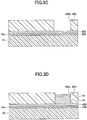
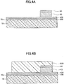
- Figs. 3A to 4D are diagrams illustrating a process of manufacturing the strain gauge according to the first embodiment, and each illustrate a cross section corresponding to Fig. 2 .
- the substrate 10 is prepared and the metallic layer 300 is formed on the upper surface 10a of the substrate 10.
- the metallic layer 300 is finally patterned to become a layer that constitutes the resistor 30 and the terminal sections 41.
- the material and thickness of the metallic layer 300 are the same as the material and thickness for each of the resistor 30 and the terminal sections 41, as described above.
- the metallic layer 300 can be deposited by magnetron sputtering in which, for example, a raw material capable of forming the metallic layer 300 is the target.
- the metallic layer 300 may be deposited by reactive sputtering, vapor deposition, arc ion plating, pulsed laser deposition, or the like.
- a functional layer having a film thickness that is approximately between 1 nm and 100 nm is vacuum-deposited on the upper surface 10a of the substrate 10, by conventional sputtering, for example.
- the functional layer refers to a layer that has a function of promoting crystal growth of the metallic layer 300 (resistor 30) that is at least an upper layer.
- the functional layer preferably further has a function of preventing oxidation of the metallic layer 300 caused by oxygen and moisture included in the substrate 10, as well as a function of improving adhesion between the substrate 10 and the metallic layer 300.
- the functional layer may further have other functions.
- the insulating resin film that constitutes the substrate 10 contains oxygen and moisture.
- the metallic layer 300 includes Cr (chromium)
- the material of the functional layer is not particularly restricted as long as it is material having a function of promoting crystal growth of the metallic layer 300 (resistor 30) that is at least an upper layer.
- Such material can be appropriately selected for any purpose, and includes one or more types of metals selected from a group consisting of, for example, Cr (chromium), Ti (titanium), V (vanadium), Nb (niobium), Ta (tantalum), Ni (nickel), Y (yttrium), Zr (zirconium), Hf (hafnium), Si (silicon), C (carbon), Zn (zinc), Cu (copper), Bi (bismuth), Fe (iron), Mo (molybdenum), W (tungsten), Ru (ruthenium), Rh (rhodium), Re (rhenium), Os (osmium), Ir (iridium), Pt (platinum), Pd (palladium), Ag (silver), Au (gold), Co (cobalt), Mn (manganes
- Examples of the above alloy include FeCr, TiAl, FeNi, NiCr, CrCu, and the like.
- Examples of the above compound include TiN, TaN, Si 3 N 4 , TiO 2 , Ta 2 O 5 , SiO 2 , and the like.
- the functional layer can be vacuum-deposited by, for example, conventional sputtering in which a raw material capable of forming the functional layer is the target and in which an Ar (argon) gas is supplied to a chamber.
- Ar argon
- the functional layer is deposited while the upper surface 10a of the substrate 10 is etched with Ar.
- a deposited amount of films of the functional layer is minimized and thus an effect of improving adhesion can be obtained.
- the functional layer may be formed by other methods.
- the upper surface 10a of the substrate 10 is activated by plasma treatment, etc. using Ar, or the like to thereby obtain the effect of improving the adhesion; subsequently, the functional layer may be vacuum-deposited by magnetron sputtering.
- a combination of the material of the functional layer and the material of the metallic layer 300 is not particularly restricted, and can be appropriately selected for any purpose.
- Ti is used for the functional layer, and a Cr composite film formed with ⁇ -Cr (alpha-chromium) as the main component can be deposited as the metallic layer 300.
- the metallic layer 300 can be deposited by, for example, magnetron sputtering in which a raw material capable of forming the Cr composite film is the target and in which an Ar gas is supplied to a chamber.
- the metallic layer 300 may be deposited by reactive sputtering in which pure Cr is the target and in which an appropriate amount of nitrogen gas, as well as an Ar gas, are supplied to a chamber.
- a growth face of the Cr composite film is defined by the functional layer formed of Ti, and a Cr composite film that is formed with ⁇ -Cr as the main component having a stable crystalline structure can be deposited.
- Ti that constitutes the functional layer is diffused into the Cr composite film, so that the gauge characteristics are improved.
- the gauge factor of the strain gauge 1 can be 10 or more, as well as the gauge factor temperature coefficient TCS and temperature coefficient of resistance TCR can be each in the range of from -1000 ppm/° C to +1000 ppm/° C.
- the Cr composite film may include Ti or TiN (titanium nitride).
- the functional layer formed of Ti includes all functions being a function of promoting crystal growth of the metallic layer 300; a function of preventing oxidation of the metallic layer 300 caused by oxygen or moisture contained in the substrate 10; and a function of improving adhesion between the substrate 10 and the metallic layer 300.
- the functional layer is formed of Ta, Si, Al, or Fe, the functional layer also includes the same functions.
- the functional layer being provided in the lower layer of the metallic layer 300
- the crystal growth of the resistor 30 can be promoted and thus the metallic layer 300 having a stable crystalline phase can be fabricated.
- the stability of the gauge characteristics can be improved.
- the material that constitutes the functional layer is diffused into the metallic layer 300, so that the gauge characteristics of the strain gauge 1 can be thereby improved.
- a seed layer 420 as the metallic layer 42 is formed by, for example, sputtering, electroless plating, or the like, to cover an upper surface of the metallic layer 300.
- a photosensitive resist 800 is formed on the entire upper surface of the seed layer 420, and by exposing and developing, an opening 800x, which is for exposing a region in which each electrode 40A is formed, is formed.
- the resist 800 for example, a dry film resist, or the like can be used.
- a given metallic layer 43 is formed on the seed layer 420 that is exposed in the opening 800x, by for example, electrolytic plating in which the seed layer 420 is set as a power supply path, and further, a given metallic layer 44 is formed on the metallic layer 43.
- the electrolytic plating is suitable because it has high takt and allows for formation of an electrolytically plated layer having low stress, as the metallic layer 43. When the electrolytically plated layer whose thickness is increased has low stress, the warp in the strain gauge 2 can be prevented.
- the metallic layer 44 may be formed on the metallic layer 43, by electroless plating.
- the resist 800 illustrated in Fig. 3D is removed.
- the resist 800 can be removed by, for example, immersing the material of the resist 800 in a dissolvable solution.
- a photosensitive resist 810 is formed on the entire upper surface of the seed layer 420, and by exposing and developing, a planar shape that is the same as that of the resistor 30 and terminal sections 41 in Fig. 1 is patterned.
- the resist 810 for example, a dry film resist, or the like can be used.
- the resist 810 is used as an etch mask, and the metallic layer 300 and the seed layer 420 that are exposed from the resist 810 are removed, so that the resistor 30 and the terminal sections 41 each of which has the planar shape in Fig. 1 are formed.
- the resistor 30 and the terminal sections 41 each of which has the planar shape in Fig. 1 are formed.
- the resistor 30 and the terminal sections 41 each of which has the planar shape in Fig. 1 are formed.
- the functional layer is patterned in the planar shape illustrated in Fig. 1 , with etching, as is the case with the resistor 30 and the terminal sections 41. Note that at this point, the seed layer 420 is formed on the resistor 30.
- the metallic layer 43 and the metallic layer 44 are used as etch masks, and an unwanted seed layer 420 that is exposed from the metallic layer 43 and the metallic layer 44 is removed, so that the metallic layer 42 is formed.
- the unwanted seed layer 420 can be removed.
- the cover layer 60 with which the resistor 30 is coated and that exposes the electrodes 40A is formed on and above the upper surface 10a of the substrate 10, so that the strain gauge 2 is completed.
- the cover layer 60 can be fabricated, such that a thermosetting insulating resin film in a semi-cured state is laminated on the upper surface 10a of the substrate 10, and such that the resistor 30 is coated therewith and the terminal sections 41 are exposed; subsequently, heat is added and curing is performed.
- the cover layer 60 may be formed, such that a thermosetting insulating resin that is liquid or paste-like is applied to the upper surface 10a of the substrate 10, and such that the resistor 30 is coated therewith and the terminal sections 41 are exposed; subsequently, heat is added and curing is performed.
- the strain gauge 1 when the functional layer, as a base layer of the resistor 30 and the terminal sections 41, is provided on the upper surface 10a of the substrate 10, the strain gauge 1 has a cross-section shape illustrated in Fig. 5 .
- a layer expressed by the numeral 20 indicates the functional layer.
- the planar shape of the strain gauge 1 in the case of providing the functional layer 20 is the same as that in Fig. 1 .
- each electrode 40A As described above, as each electrode 40A, a given metallic layer 43 formed of a thick film (1 ⁇ m or more), which is formed of Cu, a Cu alloy, Ni, or a Ni alloy, is formed above a given terminal section 41, and further, a given metallic layer 44 formed of material (Au or Pt) that has better solder wettability than the metallic layer 43 is formed in the outermost surface layer. Thereby, dissolution of metallization can be prevented, as well as improving solder wettability.
- Modification 1 of the first embodiment provides an example of electrodes each having a layer structure different from that in the first embodiment. Note that in the modification 1 of the first embodiment, the explanation for the same components as the embodiment that has been described may be omitted.
- Fig. 6 is a cross-sectional view illustrating an example of a strain gauge according to the modification 1 of the first embodiment, and illustrates a cross section corresponding to Fig. 2 .
- the strain gauge 1A differs from the strain gauge 1 (see Fig. 2 , etc.) in that the electrodes 40A are replaced with electrodes 40B.
- the cover layer 60 may be provided to cover all portions except for the electrodes 40B.
- Each electrode 40B has a laminated structure in which a plurality of metallic layers are laminated.
- each electrode 40B includes a terminal section 41 extending from a corresponding end portion from among both end portions of the resistor 30; a metallic layer 42 formed on an upper surface of the terminal section 41; a metallic layer 43 formed on an upper surface of the metallic layer 42; a metallic layer 45 formed on an upper surface of the metallic layer 43; and a metallic layer 44 formed on an upper surface of the metallic layer 45.
- each electrode 40B has a structure in which the metallic layer 45 is provided between the metallic layer 43 and the metallic layer 44 of a given electrode 40A.
- the material of the metallic layer 45 is not particularly restricted, and can be appropriately selected for any purpose.
- Ni can be used.
- NiP nickel phosphorus
- Pd nickel phosphorus
- the metallic layer 45 Ni/Pd (a metallic layer in which a Ni layer and a Pd layer are laminated in this order) may be used.
- the thickness of the metallic layer 45 is not particularly restricted, and can be appropriately selected for any purpose. For example, the thickness is approximately between 1 ⁇ m and 2 ⁇ m.
- the metallic layer 45 can be formed on the metallic layer 43 by, for example, electrolytic plating in which the seed layer 420 is set as a power supply path.
- the number of electrode layers is not particularly restricted, and the number of layers may be increased as necessary.
- a given metallic layer 43 formed of a thick film (1 ⁇ m or more), which is formed of Cu, a Cu alloy, Ni, or a Ni alloy, is formed above a given terminal section 41, and further, a given metallic layer 44 formed of material (Au or Pt) that has better solder wettability than the metallic layer 43 is formed in the outermost surface layer.
- Modification 2 of the first embodiment provides another example of electrodes each having a different layer structure from that in the first embodiment. Note that in the modification 2 of the first embodiment, the explanation for the same components as the embodiment that has been described may be omitted.
- Fig. 7 is a cross-sectional view illustrating an example of a strain gauge according to the modification 2 of the first embodiment, and illustrates a cross section corresponding to Fig. 2 .
- the strain gauge 1B differs from the strain gauge 1A (see Fig. 6 ) in that the electrodes 40B are replaced with electrodes 40C.
- the cover layer 60 may be provided to cover all portions except for the electrodes 40C.
- Each electrode 40C has a laminated structure in which a plurality of metallic layers are laminated.
- each electrode 40C includes a terminal section 41 extending from a corresponding end portion from among both end portions of the resistor 30; a metallic layer 42 formed on an upper surface of the terminal section 41; a metallic layer 43 formed on an upper surface of the metallic layer 42; a metallic layer 45A formed on an upper surface and side surfaces of the metallic layer 43 and on side surfaces of the metallic layer 42; and a metallic layer 44A formed on an upper surface and side surfaces of the metallic layer 45A.
- the material and thickness of the metallic layers 44A and 45A can be the same as the material and thickness of the metallic layers 44 and 45.
- the metallic layer 44A is a typical example of a second metallic layer according to the present invention.
- each electrode 40C In order to form each electrode 40C, first, in the process illustrated in Fig. 3D , for example, a given metallic layer 43 is formed by, for example, electrolytic plating in which the seed layer 420 is set as a power supply path, and then the resist 800 is removed as is the case with the process illustrated in Fig. 4A , without forming a given metallic layer 44. Next, the same process as that in Figs. 4B to 4D is performed. Subsequently, a given metallic layer 45A can be formed on the upper surface and side surfaces of the metallic layer 43 and on side surfaces of the metallic layer 42, by electroless plating, for example. Additionally, a given metallic layer 44A can be formed on the upper surface and side surfaces of the metallic layer 45A, by electroless plating, for example.
- each electrode can be fabricated by appropriately using both of electrolytic plating and electroless plating.
- the metallic layer 44A of the outermost layer is formed, via the metallic layer 45A, toward the side surfaces of each of the metallic layers 42 and 43, in addition to the upper surface of the metallic layer 43.
- the effect of preventing oxidation and corrosion of Cu, a Cu alloy, Ni, or a Ni alloy that constitutes the metallic layer 43 can be further enhanced, as well as the solder wettability being able to be further improved.
- the same effect is obtained even when a given metallic layer 44A is formed directly on the upper surface and side surfaces of a given metallic layer 43 and on the side surfaces of a given metallic layer 42, without forming a given metallic layer 45A.
- the metallic layer 44A may directly or indirectly cover the upper surface and side surfaces of the metallic layer 43 and the side surfaces of the metallic layer 42.
- Example 1 multiple strain gauges 1A each of which includes the electrodes 40B were fabricated.
- Ti as the functional layer 20 which had a film thickness of 3 nm, was vacuum-deposited on the upper surface 10a of the substrate 10 that was formed of a polyimide resin having a thickness of 25 ⁇ m, by conventional sputtering.
- the strain gauge 1A with the electrodes 40B was fabricated, and the presence or absence of dissolution of metallization was checked.
- 10 types of samples in each of which Cu was used for the metallic layers 42 and 43, in each of which NiP was used for the metallic layer 45, in each of which Au was used for the metallic layer 44, and in each of which the thickness of a given metallic layer was changed were fabricated (samples No. 1 to No. 10), and then the presence or absence of dissolution of metallization was checked.
- Table 1 shows results. Note that in Table 1, the film thickness "0" indicates that no metallic layer was formed. The “poor” indicates that dissolution of metallization occurred in soldering being first performed. The “good” indicates that although no dissolution of metallization occurred in soldering being first performed, little dissolution of metallization occurred in soldering being performed second (where soldering refinement, etc. was assumed). Additionally, the “excellent” indicates that dissolution of metallization occurred neither in soldering being performed first nor second. [Table 1] SAMPLE No.
- the gauge characteristics of each sample in Example 1 were measured.
- the gauge factor of each sample in Example 1 was between 14 and 16.
- the gauge factor temperature coefficient TCS and temperature coefficient of resistance TCR were each in the range of from -1000 ppm/° C to +1000 ppm/° C.
- 1, 1A, 1B strain gauge 10 substrate, 10a upper surface, 20 functional layer, 30 resistor, 41 terminal section, 40A, 40B, 40C electrode, 42, 43, 44, 44A, 45, 45A metallic layer, 60 cover layer
Landscapes
- Physics & Mathematics (AREA)
- General Physics & Mathematics (AREA)
- Engineering & Computer Science (AREA)
- Microelectronics & Electronic Packaging (AREA)
- Electromagnetism (AREA)
- Measurement Of Length, Angles, Or The Like Using Electric Or Magnetic Means (AREA)
Abstract
Description
- The present invention relates to a strain gauge.
- A strain gauge is known to be attached to a measured object to detect strain on the measured object. The strain gauge includes a resistor that detects strain, and as resistor material, for example, material including Cr (chromium) or Ni (nickel) is used. For example, both ends of the resistor are used as electrodes, and a lead wire for an external connection, or the like is jointed with solder, between the electrodes (see, for example, Patent document 1).
- [Patent document 1] Japanese Unexamined Patent Application Publication No.
2016-74934 - However, a resistor has a thin film thickness and when both ends of the resistor are used as electrodes, dissolution of metallization easily occurs, which results in less solderability. Further, when material including Cr (chromium) or Ni (nickel) is used for the resistor, solderability further gets worse. Particularly, Cr forms an autoxidized film and thus solderability gets worse.
- In view of the point described above, an object of the present invention is to improve solderability of an electrode with respect to a strain gauge in which material including Cr (chromium) or Ni (nickel) is used for a resistor.
- A strain gauge includes a flexible substrate; a resistor formed of material including at least one from among chromium and nickel, on or above the substrate; and electrodes electrically coupled to the resistor. Each electrode includes a terminal section extending from a corresponding end portion from among end portions of the resistor; a first metallic layer formed of copper, a copper alloy, nickel, or a nickel alloy, on or above the terminal section; and a second metallic layer formed of material having better solder wettability than the first metallic layer, on or above the first metallic layer.
- According to the disclosed technique, with respect to a strain gauge in which material including Cr (chromium) or Ni (nickel) is used for a resistor, solderability of an electrode can be improved.
-
- [
Fig. 1 ]
Fig. 1 is a plan view of an example of a strain gauge according to a first embodiment; - [
Fig. 2 ]
Fig. 2 is a cross-sectional view (part 1) of an example of the strain gauge according to the first embodiment; - [
Fig. 3A ]
Fig. 3A is a diagram (part 1) illustrating an example of a process of manufacturing the strain gauge according to the first embodiment; - [
Fig. 3B ]
Fig. 3B is a diagram (part 2) illustrating an example of the process of manufacturing the strain gauge according to the first embodiment; - [
Fig. 3C ]
Fig. 3C is a diagram (part 3) illustrating an example of the process of manufacturing the strain gauge according to the first embodiment; - [
Fig. 3D ]
Fig. 3D is a diagram (part 4) illustrating an example of a process of manufacturing the strain gauge according to the first embodiment; - [
Fig. 4A ]
Fig. 4A is a diagram (part 5) illustrating an example of the process of manufacturing the strain gauge according to the first embodiment; - [
Fig. 4B ]
Fig. 4B is a diagram (part 6) illustrating an example of the process of manufacturing the strain gauge according to the first embodiment; - [
Fig. 4C ]
Fig. 4C is a diagram (part 7) illustrating an example of the process of manufacturing the strain gauge according to the first embodiment; - [
Fig. 4D ]
Fig. 4D is a diagram (part 8) illustrating an example of the process of manufacturing the strain gauge according to the first embodiment; - [
Fig. 5 ]
Fig. 5 is a cross-sectional view (part 2) of an example of a strain gauge according to the first embodiment; - [
Fig. 6 ]
Fig. 6 is a cross-sectional view of an example of a strain gauge according tomodification 1 of the first embodiment; and - [
Fig. 7 ]
Fig. 7 is a cross-sectional view of an example of a strain gauge according to modification 2 of the first embodiment. - One or more embodiments will be hereinafter described with reference to the drawings. In each figure, the same numeral numbers denote the same components; accordingly, duplicative explanations may be omitted.
-
Fig. 1 is a plan view of an example of a strain gauge according to a first embodiment.Fig. 2 is a cross-sectional view of an example of the strain gauge according to the first embodiment, and illustrates a cross section taken along the A-A line inFig. 1 . With reference toFigs. 1 and 2 , thestrain gauge 1 includes asubstrate 10, aresistor 30, andelectrodes 40A. - Note that in the present embodiment, for the sake of convenience, with respect to the
strain gauge 1, the side of thesubstrate 10 where theresistor 30 is provided is referred to as an upper side or one side; and the side of thesubstrate 10 where theresistor 30 is not provided is referred to as a lower side or another side. Further, for each component, the surface on the side where theresistor 30 is provided is referred to as one surface or an upper surface; and the surface on the side where theresistor 30 is not provided is referred to as another surface or a lower surface. However, thestrain gauge 1 can be used in a state of being upside down, or be disposed at any angle. Further, a plan view means that an object is viewed from a normal direction of anupper surface 10a of thesubstrate 10, and a planar shape refers to a shape of an object when viewed from the normal direction of theupper surface 10a of thesubstrate 10. - The
substrate 10 is a member that is a base layer for forming theresistor 30 or the like and is flexible. The thickness of thesubstrate 10 is not particularly restricted, and can be appropriately selected for any purpose. For example, such a thickness can be approximately between 5 µm and 500 µm. In particular, when the thickness of thesubstrate 10 is between 5 µm and 200 µm, it is preferable in terms of strain transfer from a flexure element surface that is bonded to a lower surface of thesubstrate 10 via an adhesive layer or the like; and dimensional stability with respect to environment, and when the thickness is 10 µm or more, it is further preferable in terms of insulation. - The
substrate 10 can be formed of an insulating resin film such as a PI (polyimide) resin, an epoxy resin, a PEEK (polyether ether ketone) resin, a PEN (polyethylene naphthalate) resin, a PET (polyethylene terephthalate) resin, a PPS (polyphenylene sulfide) resin, or a polyolefin resin. Note that the film refers to a flexible member having a thickness of about 500 µm or less. - Here, the "formed of an insulating resin film" is not intended to preclude the
substrate 10 from containing fillers, impurities, or the like in the insulating resin film. Thesubstrate 10 may be formed of, for example, an insulating resin film containing fillers such as silica or alumina. - The
resistor 30 is a thin film formed in a predetermined pattern and is a sensitive section where resistance varies according to strain. Theresistor 30 may be formed directly on theupper surface 10a of thesubstrate 10, or be formed above theupper surface 10a of thesubstrate 10, via other layer(s). Note that inFig. 1 , for the sake of convenience, theresistor 30 is illustrated in a crepe pattern. - The
resistor 30 can be formed of, for example, material including Cr (chromium); material including Ni (nickel); or material including both of Cr and Ni. In other words, theresistor 30 can be formed of material including at least one from among Cr and Ni. An example of the material including Cr includes a Cr composite film. An example of the material including nickel includes Cu-Ni (copper nickel). An example of the material including both of Cr and Ni includes Ni-Cr (nickel chromium). - Here, the Cr composite film is a composite film of Cr, CrN, Cr2N, and the like. The Cr composite film may include incidental impurities such as chromium oxide.
- The thickness of the
resistor 30 is not particularly restricted, and can be appropriately selected for any purpose. The thickness can be, for example, approximately between 0.05 µm and 2 µm. In particular, when the thickness of theresistor 30 is 0.1 µm or more, it is preferable in terms of improvement in crystallinity (e.g., crystallinity of α-Cr) of a crystal that constitutes theresistor 30, and when the thickness of theresistor 30 is 1 µm or less, it is further preferable in terms of reduction in cracks of a given film caused by internal stress of the film that constitutes theresistor 30, or reduction in warp in thesubstrate 10. - For example, when the
resistor 30 is the Cr composite film, the resistor is formed with α-Cr (alpha-chromium) as the main component having a stable crystalline phase, so that stability of the gauge characteristics can be improved. Additionally, when theresistor 30 is formed with α-Cr as the main component, the gauge factor of thestrain gauge 1 can be 10 or more, as well as a gauge factor temperature coefficient TCS and temperature coefficient of resistance TCR can be each in the range of from -1000 ppm/°C to +1000 ppm/°C. Here, a main component means that a target substance has 50% by weight or more of total substances that constitute the resistor. Theresistor 30 preferably includes α-Cr of 80% by weight or more, from the viewpoint of improving the gauge characteristics. Note that α-Cr is Cr having a bcc structure (body-centered cubic structure). - The
electrodes 40A respectively extend from both end portions of theresistor 30 and are each wider than theresistor 30 to be in an approximately rectangular shape, in a plan view. Theelectrodes 40A are a pair of electrodes from which a change in a resistance value of theresistor 30 according to strain is output externally, where, for example, a lead wire for an external connection, or the like is joined. For example, theresistor 30 extends zigzagged back and forth from one of theelectrodes 40A to anotherelectrode 40A. - Each
electrode 40A has a laminated structure in which a plurality of metallic layers are laminated. Specifically, eachelectrode 40A includes aterminal section 41 extending from a corresponding end portion from among both end portions of theresistor 30; ametallic layer 42 formed on an upper surface of theterminal section 41; ametallic layer 43 formed on an upper surface of themetallic layer 42; and ametallic layer 44 formed on an upper surface of themetallic layer 43. Note that for the sake of convenience, theresistor 30 and theterminal sections 41 are expressed by different numerals. However, the resistor and the terminal sections can be integrally formed of the same material, in the same process. Themetallic layer 43 is a typical example of a first metallic layer according to the present invention, and themetallic layer 44 is a typical example of a second metallic layer according to the present invention. - The material of the
metallic layer 42 is not particularly restricted, and can be appropriately selected for any purpose. For example, Cu (copper) can be used. The thickness of themetallic layer 42 is not particularly restricted, and can be appropriately selected for any purpose. For example, the thickness can be approximately in the range of from 0.01 µm to 1 µm. - Preferably, the material of the
metallic layer 43 includes Cu, a Cu alloy, Ni, or a Ni alloy. The thickness of themetallic layer 43 is determined in consideration of solderability to theelectrode 40A, and is preferably 1 µm or more, and more preferably 3 µm or more. When the material of themetallic layer 43 includes Cu, a Cu alloy, Ni, or a Ni alloy and the thickness of themetallic layer 43 is 1 µm or more, dissolution of metallization is ameliorated. Also, when the material of themetallic layer 43 includes Cu, a Cu alloy, Ni, or a Ni alloy and the thickness of themetallic layer 43 is 3 µm or more, dissolution of metallization is further ameliorated. Note that the thickness of themetallic layer 43 is preferably 30 µm or less in terms of ease of electrolytic plating. - Here, the dissolution of metallization means that the material constituting the
electrode 40A is dissolved in solder for jointing theelectrode 40A, and that the thickness ofelectrode 40A is reduced or the material disappears. When the dissolution of metallization occurs, adhesion strength or tensile strength with a lead wire, or the like to be jointed to theelectrode 40A may be reduced. Thus, it is preferable that no dissolution of metallization occur. - For the material of the
metallic layer 44, material having better solder wettability than themetallic layer 43 can be selected. For example, when the material of themetallic layer 43 includes Cu, a Cu alloy, Ni, or a Ni alloy, the material of themetallic layer 44 can include Au (gold). When the surface of Cu, a Cu alloy, Ni, or a Ni alloy is coated with Au, oxidation and corrosion for Cu, a Cu alloy, Ni, or a Ni alloy can be prevented, as well as good solder wettability can be provided. Instead of Au, when the material of themetallic layer 44 includes Pt (platinum), themetallic layer 44 has the same effect. The thickness of themetallic layer 44 is not particularly restricted, and can be appropriately selected for any purpose. For example, the thickness can be approximately between 0.01 µm and 1 µm. - Note that each
terminal section 41 is exposed around a given laminated section of themetallic layers terminal section 41 may have the same planar shape as the laminated section of themetallic layers - A cover layer 60 (insulating resin layer) may be disposed on and above the
upper surface 10a of thesubstrate 10, such that theresistor 30 is coated and theelectrodes 40A are exposed. With thecover layer 60 being provided, mechanical damage, and the like can be prevented from occurring in theresistor 30. Additionally, with thecover layer 60 being provided, theresistor 30 can be protected against moisture, and the like. Note that thecover layer 60 may be provided to cover all portions except for theelectrodes 40A. - The
cover layer 60 can be formed of an insulating resin such as a PI resin, an epoxy resin, a PEEK resin, a PEN resin, a PET resin, or a PPS resin, a composite resin (e.g., a silicone resin or a polyolefin resin). Thecover layer 60 may contain fillers or pigments. The thickness of thecover layer 60 is not particularly restricted, and can be appropriately selected for any purpose. For example, the thickness may be approximately between 2 µm and 30 µm. -
Figs. 3A to 4D are diagrams illustrating a process of manufacturing the strain gauge according to the first embodiment, and each illustrate a cross section corresponding toFig. 2 . In order to manufacture thestrain gauge 1, first, in the process illustrated inFig. 3A , thesubstrate 10 is prepared and themetallic layer 300 is formed on theupper surface 10a of thesubstrate 10. Themetallic layer 300 is finally patterned to become a layer that constitutes theresistor 30 and theterminal sections 41. In this case, the material and thickness of themetallic layer 300 are the same as the material and thickness for each of theresistor 30 and theterminal sections 41, as described above. - The
metallic layer 300 can be deposited by magnetron sputtering in which, for example, a raw material capable of forming themetallic layer 300 is the target. Instead of magnetron sputtering, themetallic layer 300 may be deposited by reactive sputtering, vapor deposition, arc ion plating, pulsed laser deposition, or the like. - From the viewpoint of stabilizing the gauge characteristics, before depositing the
metallic layer 300, preferably, as a base layer, a functional layer having a film thickness that is approximately between 1 nm and 100 nm is vacuum-deposited on theupper surface 10a of thesubstrate 10, by conventional sputtering, for example. - In the present application, the functional layer refers to a layer that has a function of promoting crystal growth of the metallic layer 300 (resistor 30) that is at least an upper layer. The functional layer preferably further has a function of preventing oxidation of the
metallic layer 300 caused by oxygen and moisture included in thesubstrate 10, as well as a function of improving adhesion between thesubstrate 10 and themetallic layer 300. The functional layer may further have other functions. - The insulating resin film that constitutes the
substrate 10 contains oxygen and moisture. In this regard, particularly when themetallic layer 300 includes Cr (chromium), it is effective for the functional layer to have a function of preventing oxidation of themetallic layer 300, because Cr forms an autoxidized film. - The material of the functional layer is not particularly restricted as long as it is material having a function of promoting crystal growth of the metallic layer 300 (resistor 30) that is at least an upper layer. Such material can be appropriately selected for any purpose, and includes one or more types of metals selected from a group consisting of, for example, Cr (chromium), Ti (titanium), V (vanadium), Nb (niobium), Ta (tantalum), Ni (nickel), Y (yttrium), Zr (zirconium), Hf (hafnium), Si (silicon), C (carbon), Zn (zinc), Cu (copper), Bi (bismuth), Fe (iron), Mo (molybdenum), W (tungsten), Ru (ruthenium), Rh (rhodium), Re (rhenium), Os (osmium), Ir (iridium), Pt (platinum), Pd (palladium), Ag (silver), Au (gold), Co (cobalt), Mn (manganese), and Al (aluminum); an alloy of any metals from among the group; or a compound of any metal from among the group.
- Examples of the above alloy include FeCr, TiAl, FeNi, NiCr, CrCu, and the like. Examples of the above compound include TiN, TaN, Si3N4, TiO2, Ta2O5, SiO2, and the like.
- The functional layer can be vacuum-deposited by, for example, conventional sputtering in which a raw material capable of forming the functional layer is the target and in which an Ar (argon) gas is supplied to a chamber. By using conventional sputtering, the functional layer is deposited while the
upper surface 10a of thesubstrate 10 is etched with Ar. Thus, a deposited amount of films of the functional layer is minimized and thus an effect of improving adhesion can be obtained. - However, this is an example of a method of depositing the functional layer, and the functional layer may be formed by other methods. For example, before depositing the functional layer, the
upper surface 10a of thesubstrate 10 is activated by plasma treatment, etc. using Ar, or the like to thereby obtain the effect of improving the adhesion; subsequently, the functional layer may be vacuum-deposited by magnetron sputtering. - A combination of the material of the functional layer and the material of the
metallic layer 300 is not particularly restricted, and can be appropriately selected for any purpose. For example, Ti is used for the functional layer, and a Cr composite film formed with α-Cr (alpha-chromium) as the main component can be deposited as themetallic layer 300. - In this case, the
metallic layer 300 can be deposited by, for example, magnetron sputtering in which a raw material capable of forming the Cr composite film is the target and in which an Ar gas is supplied to a chamber. Alternatively, themetallic layer 300 may be deposited by reactive sputtering in which pure Cr is the target and in which an appropriate amount of nitrogen gas, as well as an Ar gas, are supplied to a chamber. - In such methods, a growth face of the Cr composite film is defined by the functional layer formed of Ti, and a Cr composite film that is formed with α-Cr as the main component having a stable crystalline structure can be deposited. Also, Ti that constitutes the functional layer is diffused into the Cr composite film, so that the gauge characteristics are improved. For example, the gauge factor of the
strain gauge 1 can be 10 or more, as well as the gauge factor temperature coefficient TCS and temperature coefficient of resistance TCR can be each in the range of from -1000 ppm/° C to +1000 ppm/° C. Note that, when the functional layer is formed of Ti, the Cr composite film may include Ti or TiN (titanium nitride). - Note that when the
metallic layer 300 is a Cr composite film, the functional layer formed of Ti includes all functions being a function of promoting crystal growth of themetallic layer 300; a function of preventing oxidation of themetallic layer 300 caused by oxygen or moisture contained in thesubstrate 10; and a function of improving adhesion between thesubstrate 10 and themetallic layer 300. Instead of Ti, when the functional layer is formed of Ta, Si, Al, or Fe, the functional layer also includes the same functions. - As described above, with the functional layer being provided in the lower layer of the
metallic layer 300, the crystal growth of theresistor 30 can be promoted and thus themetallic layer 300 having a stable crystalline phase can be fabricated. As a result, with respect to thestrain gauge 1, the stability of the gauge characteristics can be improved. Also, the material that constitutes the functional layer is diffused into themetallic layer 300, so that the gauge characteristics of thestrain gauge 1 can be thereby improved. - Next, in the process illustrated in
Fig. 3B , aseed layer 420 as themetallic layer 42 is formed by, for example, sputtering, electroless plating, or the like, to cover an upper surface of themetallic layer 300. - Next, in the process illustrated in
Fig. 3C , a photosensitive resist 800 is formed on the entire upper surface of theseed layer 420, and by exposing and developing, anopening 800x, which is for exposing a region in which eachelectrode 40A is formed, is formed. As the resist 800, for example, a dry film resist, or the like can be used. - Next, in the process illustrated in
Fig. 3D , a givenmetallic layer 43 is formed on theseed layer 420 that is exposed in theopening 800x, by for example, electrolytic plating in which theseed layer 420 is set as a power supply path, and further, a givenmetallic layer 44 is formed on themetallic layer 43. The electrolytic plating is suitable because it has high takt and allows for formation of an electrolytically plated layer having low stress, as themetallic layer 43. When the electrolytically plated layer whose thickness is increased has low stress, the warp in the strain gauge 2 can be prevented. Note that themetallic layer 44 may be formed on themetallic layer 43, by electroless plating. - Note that in forming the
metallic layer 44, side surfaces of themetallic layer 43 are coated with the resist 800, so that themetallic layer 44 is formed only on the upper surface of themetallic layer 43 and is not on the side surfaces thereof. - Next, in the process illustrated in
Fig. 4A , the resist 800 illustrated inFig. 3D is removed. The resist 800 can be removed by, for example, immersing the material of the resist 800 in a dissolvable solution. - Next, in the process illustrated in
Fig. 4B , a photosensitive resist 810 is formed on the entire upper surface of theseed layer 420, and by exposing and developing, a planar shape that is the same as that of theresistor 30 andterminal sections 41 inFig. 1 is patterned. As the resist 810, for example, a dry film resist, or the like can be used. - Next, in the process illustrated in
Fig. 4C , the resist 810 is used as an etch mask, and themetallic layer 300 and theseed layer 420 that are exposed from the resist 810 are removed, so that theresistor 30 and theterminal sections 41 each of which has the planar shape inFig. 1 are formed. For example, with wet etching, unwanted portions of themetallic layer 300 and theseed layer 420 can be removed. When a functional layer is formed in a lower layer of themetallic layer 300, the functional layer is patterned in the planar shape illustrated inFig. 1 , with etching, as is the case with theresistor 30 and theterminal sections 41. Note that at this point, theseed layer 420 is formed on theresistor 30. - Next, in the process illustrated in
Fig. 4D , themetallic layer 43 and themetallic layer 44 are used as etch masks, and anunwanted seed layer 420 that is exposed from themetallic layer 43 and themetallic layer 44 is removed, so that themetallic layer 42 is formed. For example, by wet etching using etching liquid with which theseed layer 420 is etched and with which the functional layer and theresistor 30 are not etched, theunwanted seed layer 420 can be removed. - After the process illustrated in
Fig. 4D , thecover layer 60 with which theresistor 30 is coated and that exposes theelectrodes 40A is formed on and above theupper surface 10a of thesubstrate 10, so that the strain gauge 2 is completed. For example, thecover layer 60 can be fabricated, such that a thermosetting insulating resin film in a semi-cured state is laminated on theupper surface 10a of thesubstrate 10, and such that theresistor 30 is coated therewith and theterminal sections 41 are exposed; subsequently, heat is added and curing is performed. Thecover layer 60 may be formed, such that a thermosetting insulating resin that is liquid or paste-like is applied to theupper surface 10a of thesubstrate 10, and such that theresistor 30 is coated therewith and theterminal sections 41 are exposed; subsequently, heat is added and curing is performed. - Note that when the functional layer, as a base layer of the
resistor 30 and theterminal sections 41, is provided on theupper surface 10a of thesubstrate 10, thestrain gauge 1 has a cross-section shape illustrated inFig. 5 . A layer expressed by the numeral 20 indicates the functional layer. The planar shape of thestrain gauge 1 in the case of providing thefunctional layer 20 is the same as that inFig. 1 . - As described above, as each
electrode 40A, a givenmetallic layer 43 formed of a thick film (1 µm or more), which is formed of Cu, a Cu alloy, Ni, or a Ni alloy, is formed above a giventerminal section 41, and further, a givenmetallic layer 44 formed of material (Au or Pt) that has better solder wettability than themetallic layer 43 is formed in the outermost surface layer. Thereby, dissolution of metallization can be prevented, as well as improving solder wettability. -
Modification 1 of the first embodiment provides an example of electrodes each having a layer structure different from that in the first embodiment. Note that in themodification 1 of the first embodiment, the explanation for the same components as the embodiment that has been described may be omitted. -
Fig. 6 is a cross-sectional view illustrating an example of a strain gauge according to themodification 1 of the first embodiment, and illustrates a cross section corresponding toFig. 2 . With reference toFig. 6 , thestrain gauge 1A differs from the strain gauge 1 (seeFig. 2 , etc.) in that theelectrodes 40A are replaced withelectrodes 40B. Note that thecover layer 60 may be provided to cover all portions except for theelectrodes 40B. - Each
electrode 40B has a laminated structure in which a plurality of metallic layers are laminated. Specifically, eachelectrode 40B includes aterminal section 41 extending from a corresponding end portion from among both end portions of theresistor 30; ametallic layer 42 formed on an upper surface of theterminal section 41; ametallic layer 43 formed on an upper surface of themetallic layer 42; ametallic layer 45 formed on an upper surface of themetallic layer 43; and ametallic layer 44 formed on an upper surface of themetallic layer 45. In other words, eachelectrode 40B has a structure in which themetallic layer 45 is provided between themetallic layer 43 and themetallic layer 44 of a givenelectrode 40A. - The material of the
metallic layer 45 is not particularly restricted, and can be appropriately selected for any purpose. For example, Ni can be used. Instead of Ni, NiP (nickel phosphorus) or Pd may be used. Also, as themetallic layer 45, Ni/Pd (a metallic layer in which a Ni layer and a Pd layer are laminated in this order) may be used. The thickness of themetallic layer 45 is not particularly restricted, and can be appropriately selected for any purpose. For example, the thickness is approximately between 1 µm and 2 µm. - In the process illustrated in
Fig. 3D , themetallic layer 45 can be formed on themetallic layer 43 by, for example, electrolytic plating in which theseed layer 420 is set as a power supply path. - In such a manner, the number of electrode layers is not particularly restricted, and the number of layers may be increased as necessary. In this case as well, a given
metallic layer 43 formed of a thick film (1 µm or more), which is formed of Cu, a Cu alloy, Ni, or a Ni alloy, is formed above a giventerminal section 41, and further, a givenmetallic layer 44 formed of material (Au or Pt) that has better solder wettability than themetallic layer 43 is formed in the outermost surface layer. Thereby, as is the case with the first embodiment, the dissolution of metallization can be prevented, as well as improving the solder wettability. - Modification 2 of the first embodiment provides another example of electrodes each having a different layer structure from that in the first embodiment. Note that in the modification 2 of the first embodiment, the explanation for the same components as the embodiment that has been described may be omitted.
-
Fig. 7 is a cross-sectional view illustrating an example of a strain gauge according to the modification 2 of the first embodiment, and illustrates a cross section corresponding toFig. 2 . With reference toFig. 7 , thestrain gauge 1B differs from thestrain gauge 1A (seeFig. 6 ) in that theelectrodes 40B are replaced withelectrodes 40C. Note that thecover layer 60 may be provided to cover all portions except for theelectrodes 40C. - Each
electrode 40C has a laminated structure in which a plurality of metallic layers are laminated. Specifically, eachelectrode 40C includes aterminal section 41 extending from a corresponding end portion from among both end portions of theresistor 30; ametallic layer 42 formed on an upper surface of theterminal section 41; ametallic layer 43 formed on an upper surface of themetallic layer 42; ametallic layer 45A formed on an upper surface and side surfaces of themetallic layer 43 and on side surfaces of themetallic layer 42; and ametallic layer 44A formed on an upper surface and side surfaces of themetallic layer 45A. For example, the material and thickness of themetallic layers metallic layers metallic layer 44A is a typical example of a second metallic layer according to the present invention. - In order to form each
electrode 40C, first, in the process illustrated inFig. 3D , for example, a givenmetallic layer 43 is formed by, for example, electrolytic plating in which theseed layer 420 is set as a power supply path, and then the resist 800 is removed as is the case with the process illustrated inFig. 4A , without forming a givenmetallic layer 44. Next, the same process as that inFigs. 4B to 4D is performed. Subsequently, a givenmetallic layer 45A can be formed on the upper surface and side surfaces of themetallic layer 43 and on side surfaces of themetallic layer 42, by electroless plating, for example. Additionally, a givenmetallic layer 44A can be formed on the upper surface and side surfaces of themetallic layer 45A, by electroless plating, for example. - As described above, each electrode can be fabricated by appropriately using both of electrolytic plating and electroless plating. In the structure of each electrode 40C, a given
metallic layer 43 formed of a thick film (1 µm or more), which is formed of Cu, a Cu alloy, Ni, or a Ni alloy, is formed above a giventerminal section 41, and further, a givenmetallic layer 44A formed of material (Au or Pt) that has better solder wettability than themetallic layer 43 is formed in the outermost layer. Note, however, that themetallic layer 44A of the outermost layer is formed, via themetallic layer 45A, toward the side surfaces of each of themetallic layers metallic layer 43. Thus, in comparison to theelectrodes 40A or theelectrodes 40B, the effect of preventing oxidation and corrosion of Cu, a Cu alloy, Ni, or a Ni alloy that constitutes themetallic layer 43 can be further enhanced, as well as the solder wettability being able to be further improved. - Note that the same effect is obtained even when a given
metallic layer 44A is formed directly on the upper surface and side surfaces of a givenmetallic layer 43 and on the side surfaces of a givenmetallic layer 42, without forming a givenmetallic layer 45A. In other words, themetallic layer 44A may directly or indirectly cover the upper surface and side surfaces of themetallic layer 43 and the side surfaces of themetallic layer 42. - In Example 1,
multiple strain gauges 1A each of which includes theelectrodes 40B were fabricated. - First, Ti as the
functional layer 20, which had a film thickness of 3 nm, was vacuum-deposited on theupper surface 10a of thesubstrate 10 that was formed of a polyimide resin having a thickness of 25 µm, by conventional sputtering. - Then, patterning was finally performed on the
functional layer 20, by magnetron sputtering, so that themetallic layer 300 that constituted theresistor 30 and theterminal sections 41 was deposited. - Next, the process illustrated in
Figs. 3B to 4D was modified as described in themodification 1 of the first embodiment, thestrain gauge 1A with theelectrodes 40B was fabricated, and the presence or absence of dissolution of metallization was checked. Specifically, 10 types of samples in each of which Cu was used for themetallic layers metallic layer 45, in each of which Au was used for themetallic layer 44, and in each of which the thickness of a given metallic layer was changed were fabricated (samples No. 1 to No. 10), and then the presence or absence of dissolution of metallization was checked. - Table 1 shows results. Note that in Table 1, the film thickness "0" indicates that no metallic layer was formed. The "poor" indicates that dissolution of metallization occurred in soldering being first performed. The "good" indicates that although no dissolution of metallization occurred in soldering being first performed, little dissolution of metallization occurred in soldering being performed second (where soldering refinement, etc. was assumed). Additionally, the "excellent" indicates that dissolution of metallization occurred neither in soldering being performed first nor second.
[Table 1] SAMPLE No. EACH FILM THICKNESS [µm] SOLDERABILITY Cu NiP Au 1 0.5 0 0 POOR PRESENCE OF DISSOLUTION OF METALLIZATION 2 0.5 0 0.1 POOR PRESENCE OF DISSOLUTION OF METALLIZATION 3 0.5 0 0.8 POOR PRESENCE OF DISSOLUTION OF METALLIZATION 4 1 1 0.1 GOOD ABSENCE OF DISSOLUTION OF METALLIZATION 5 3 0 0 EXCELLENT ABSENCE OF DISSOLUTION OF METALLIZATION 6 3 0 0.1 EXCELLENT ABSENCE OF DISSOLUTION OF METALLIZATION 7 3 0 0.8 EXCELLENT ABSENCE OF DISSOLUTION OF METALLIZATION 8 3 1 0.1 EXCELLENT ABSENCE OF DISSOLUTION OF METALLIZATION 9 5 1 0.1 EXCELLENT ABSENCE OF DISSOLUTION OF METALLIZATION 10 8 1 0.1 EXCELLENT ABSENCE OF DISSOLUTION OF METALLIZATION - As shown in Table 1, it was confirmed that when the thickness of Cu was 1 µm or more, dissolution of metallization was improved, and that when the thickness was 3 µm or more, the dissolution of metallization was further improved. Additionally, from the results for
sample 1 and sample 5, it was confirmed that the presence or absence of dissolution of metallization was determined only according to the thickness of Cu and was not determined upon the presence or absence of each of NiP and Au. Note, however, that as described above, in order to prevent dissolution of metallization and improve solder wettability, a metallic layer formed of Au or an equivalent material (Pt, etc.) is required. - Then, the gauge characteristics of each sample in Example 1 were measured. As a result, the gauge factor of each sample in Example 1 was between 14 and 16. Also, for each sample in Example 1, the gauge factor temperature coefficient TCS and temperature coefficient of resistance TCR were each in the range of from -1000 ppm/° C to +1000 ppm/° C.
- As described above, with the
functional layer 20 formed of Ti being provided, crystal growth of α-Cr was promoted and a Cr composite film was formed with α-Cr as the main component, so that a strain gauge that had a gauge factor of 10 or more, and that had the gauge factor temperature coefficient TCS and temperature coefficient of resistance TCR being each in the range of from -1000 ppm/° C to +1000 ppm/° C, was fabricated. Note that the diffusion effect of Ti into the Cr composite film is considered to cause the improvement in the gauge characteristics. - The preferred embodiment and the like have been described above in detail, but are not limited thereto. Various modifications and alternatives to the above embodiment and the like can be made without departing from a scope set forth in the claims.
- This International application claims priority to Japanese Patent Application Nos.
2017-191823, filed September 29, 2017 2018-052421, filed March 20, 2018 - 1, 1A, 1B strain gauge, 10 substrate, 10a upper surface, 20 functional layer, 30 resistor, 41 terminal section, 40A, 40B, 40C electrode, 42, 43, 44, 44A, 45, 45A metallic layer, 60 cover layer
Claims (12)
- A strain gauge comprising:a flexible substrate;a resistor formed of material including at least one from among chromium and nickel, on or above the substrate; andelectrodes electrically coupled to the resistor, each electrode including:a terminal section extending from a corresponding end portion from among end portions of the resistor;a first metallic layer formed of copper, a copper alloy, nickel, or a nickel alloy, on or above the terminal section; anda second metallic layer formed of material having better solder wettability than the first metallic layer, on or above the first metallic layer.
- The strain gauge according to claim 1, wherein the first metallic layer is an electrolytically plated layer.
- The strain gauge according to claim 1 or 2, wherein the second metallic layer directly or indirectly covers an upper surface and side surfaces of the first metallic layer.
- The strain gauge according to any one of claims 1 to 3, wherein the first metallic layer has a thickness of 1 µm or more.
- The strain gauge according to claim 4, wherein the first metallic layer has a thickness of 3 µm or more.
- The strain gauge according to any one of claims 1 to 5, further comprising a seed layer between the terminal section and the first metallic layer.
- The strain gauge according to any one of claims 1 to 6, wherein a main component of the resistor is alpha-chromium.
- The strain gauge according to claim 7, wherein the resistor includes alpha-chromium of 80% by weight or more.
- The strain gauge according to claim 7 or 8, wherein the resistor includes chromium nitride.
- The strain gauge according to any one of claims 1 to 9, further comprising a functional layer formed of a metal, an alloy, or a metal compound, on one surface of the substrate, and
wherein the resistor is formed on one surface of the functional layer. - The strain gauge according to claim 10, wherein the functional layer includes a function of promoting crystal growth of the resistor.
- The strain gauge according to any one of claims 1 to 11, further comprising an insulating resin layer with which the resistor is coated.
Applications Claiming Priority (3)
| Application Number | Priority Date | Filing Date | Title |
|---|---|---|---|
| JP2017191823 | 2017-09-29 | ||
| JP2018052421A JP2019066453A (en) | 2017-09-29 | 2018-03-20 | Strain gauge |
| PCT/JP2018/035939 WO2019065841A1 (en) | 2017-09-29 | 2018-09-27 | Strain gauge |
Publications (2)
| Publication Number | Publication Date |
|---|---|
| EP3690389A1 true EP3690389A1 (en) | 2020-08-05 |
| EP3690389A4 EP3690389A4 (en) | 2021-07-21 |
Family
ID=65903563
Family Applications (1)
| Application Number | Title | Priority Date | Filing Date |
|---|---|---|---|
| EP18863695.5A Pending EP3690389A4 (en) | 2017-09-29 | 2018-09-27 | EXTENSION KNIFE |
Country Status (5)
| Country | Link |
|---|---|
| US (1) | US11543308B2 (en) |
| EP (1) | EP3690389A4 (en) |
| JP (3) | JP2019066453A (en) |
| CN (1) | CN111406196B (en) |
| WO (1) | WO2019065841A1 (en) |
Cited By (1)
| Publication number | Priority date | Publication date | Assignee | Title |
|---|---|---|---|---|
| EP4123283A1 (en) * | 2021-07-21 | 2023-01-25 | Hahn-Schickard-Gesellschaft für angewandte Forschung e.V. | Mechanical coupling method for sensors for detecting mechanical stresses |
Families Citing this family (22)
| Publication number | Priority date | Publication date | Assignee | Title |
|---|---|---|---|---|
| JP2019066453A (en) | 2017-09-29 | 2019-04-25 | ミネベアミツミ株式会社 | Strain gauge |
| JP2019066312A (en) * | 2017-09-29 | 2019-04-25 | ミネベアミツミ株式会社 | Strain gauge |
| JP2019066454A (en) * | 2017-09-29 | 2019-04-25 | ミネベアミツミ株式会社 | Strain gauge and sensor module |
| JP6793103B2 (en) | 2017-09-29 | 2020-12-02 | ミネベアミツミ株式会社 | Strain gauge |
| JP2019078726A (en) * | 2017-10-27 | 2019-05-23 | ミネベアミツミ株式会社 | Strain gauge and sensor module |
| JP2019082424A (en) * | 2017-10-31 | 2019-05-30 | ミネベアミツミ株式会社 | Strain gauge |
| JP2019113411A (en) | 2017-12-22 | 2019-07-11 | ミネベアミツミ株式会社 | Strain gauge and sensor module |
| JP2019184344A (en) | 2018-04-05 | 2019-10-24 | ミネベアミツミ株式会社 | Strain gauge and manufacturing method therefor |
| WO2020085247A1 (en) | 2018-10-23 | 2020-04-30 | ミネベアミツミ株式会社 | Accelerator pedal, steering apparatus, 6-axis sensor, engine, bumper, and the like |
| JP7303663B2 (en) * | 2019-05-15 | 2023-07-05 | ミネベアミツミ株式会社 | Strain gauge, sensor module, connection structure |
| JP7201542B2 (en) * | 2019-06-21 | 2023-01-10 | ミネベアミツミ株式会社 | Rolling bearing, rotating device, bearing monitoring device, bearing monitoring method |
| JP7426794B2 (en) * | 2019-10-01 | 2024-02-02 | ミネベアミツミ株式会社 | sensor module |
| JP7406517B2 (en) * | 2020-03-24 | 2023-12-27 | ミネベアミツミ株式会社 | strain gauge |
| JP2021162303A (en) | 2020-03-30 | 2021-10-11 | ミネベアミツミ株式会社 | Strain gauge |
| JP7736429B2 (en) * | 2020-10-30 | 2025-09-09 | 日東電工株式会社 | Laminated film, method for manufacturing second laminated film, and method for manufacturing strain sensor |
| JP2022106507A (en) | 2021-01-07 | 2022-07-20 | ミネベアミツミ株式会社 | Strain gauge |
| JP7189240B2 (en) * | 2021-01-18 | 2022-12-13 | ミネベアミツミ株式会社 | strain gauge |
| US20220301747A1 (en) * | 2021-03-19 | 2022-09-22 | Holy Stone Enterprise Co., Ltd. | High-Power Resistor |
| WO2023276365A1 (en) * | 2021-07-02 | 2023-01-05 | ミネベアミツミ株式会社 | Rolling bearing |
| JP2023067057A (en) * | 2021-10-29 | 2023-05-16 | ミネベアミツミ株式会社 | strain gauge module |
| CN115323337B (en) * | 2022-10-11 | 2023-01-10 | 松诺盟科技有限公司 | Nano-film composite strain sensor and preparation method and application thereof |
| CN119043562B (en) * | 2024-10-29 | 2025-01-28 | 氢联(江苏)高科技有限公司 | Air pressure detection method and system in argon recovery and purification process |
Family Cites Families (114)
| Publication number | Priority date | Publication date | Assignee | Title |
|---|---|---|---|---|
| US3867231A (en) | 1972-06-28 | 1975-02-18 | Goodyear Tire & Rubber | Tire building machine |
| JPS54129889A (en) * | 1978-03-31 | 1979-10-08 | Hitachi Ltd | Strain measuring unit |
| JPS5511320A (en) * | 1978-07-10 | 1980-01-26 | Hitachi Ltd | Semiconductor displacement converter |
| JPS5897607A (en) | 1981-12-07 | 1983-06-10 | Kyowa Dengiyou:Kk | Strain gauge |
| JPS58169150A (en) | 1982-03-30 | 1983-10-05 | Fujitsu Ltd | Manufacture of photomask |
| DE3403042A1 (en) | 1984-01-30 | 1985-08-01 | Philips Patentverwaltung Gmbh, 2000 Hamburg | THIN FILM STRETCH MEASUREMENT STRIP SYSTEM AND METHOD FOR THE PRODUCTION THEREOF |
| US4658233A (en) | 1984-03-16 | 1987-04-14 | Fuji Electric Corporate Research & Development Ltd. | Strain gauge |
| DE3429649A1 (en) | 1984-08-11 | 1986-02-20 | Vdo Adolf Schindling Ag, 6000 Frankfurt | ELECTRICAL RESISTANCE |
| JPS61176803A (en) | 1985-01-31 | 1986-08-08 | Hitachi Ltd | strain gauge |
| JPS61288401A (en) * | 1985-06-14 | 1986-12-18 | 株式会社村田製作所 | Thin film resistor |
| JPS63165725A (en) | 1986-12-26 | 1988-07-09 | Aisin Seiki Co Ltd | Strain gauge for pressure sensor |
| JP2516964B2 (en) | 1987-03-31 | 1996-07-24 | 鐘淵化学工業株式会社 | Strain sensor |
| US4937550A (en) | 1987-03-31 | 1990-06-26 | Kanegafuchi Kagaku Kogyo Kabushiki Kaisha | Strain sensor |
| JP2585681B2 (en) * | 1988-02-08 | 1997-02-26 | 株式会社タイセー | Metal thin film resistive strain gauge |
| JPH0270201A (en) * | 1988-09-03 | 1990-03-09 | Fuji Electric Co Ltd | Auxiliary power source equipment for vehicle |
| JPH02189981A (en) | 1989-01-19 | 1990-07-25 | Ricoh Co Ltd | Semiconductor device and manufacture thereof |
| JPH0495738A (en) | 1990-08-06 | 1992-03-27 | Teraoka Seiko Co Ltd | Load cell |
| US5154247A (en) | 1989-10-31 | 1992-10-13 | Teraoka Seiko Co., Limited | Load cell |
| JPH03191802A (en) | 1989-12-21 | 1991-08-21 | Sumitomo Electric Ind Ltd | strain sensitive element |
| JP2890601B2 (en) | 1990-02-08 | 1999-05-17 | 株式会社デンソー | Semiconductor sensor |
| WO1991017415A1 (en) | 1990-05-07 | 1991-11-14 | Robert Bosch Gmbh | Process and device for the manufacture of a pressure force sensor |
| JPH0438402A (en) | 1990-06-02 | 1992-02-07 | Kyowa Electron Instr Co Ltd | Strain gage and its manufacture |
| JPH05308107A (en) | 1991-07-01 | 1993-11-19 | Sumitomo Electric Ind Ltd | Semiconductor device and its manufacture |
| JPH0580070A (en) | 1991-09-24 | 1993-03-30 | Aisin Seiki Co Ltd | Strain gauge element and manufacture thereof |
| JPH05145142A (en) | 1991-11-19 | 1993-06-11 | Matsushita Electric Ind Co Ltd | Magnetoresistive element |
| JPH06137804A (en) * | 1992-02-13 | 1994-05-20 | Tama Electric Co Ltd | Metal thin film resistance strain gauge |
| US5328551A (en) | 1992-10-28 | 1994-07-12 | Eaton Corporation | Method of making high output strain gage |
| JPH06176903A (en) | 1992-12-03 | 1994-06-24 | Nippon Soken Inc | Electrode structure of Cr-based cermet thin film |
| JPH06300649A (en) * | 1993-04-12 | 1994-10-28 | Sumitomo Electric Ind Ltd | Thin film strain resistance material, fabrication thereof and thin film strain sensor |
| JPH07113697A (en) * | 1993-10-19 | 1995-05-02 | Tec Corp | Load cell |
| JPH07307210A (en) * | 1994-05-12 | 1995-11-21 | Matsushita Electric Ind Co Ltd | Metal resistor manufacturing method and mechanical sensor |
| JP3233248B2 (en) * | 1994-05-13 | 2001-11-26 | エヌオーケー株式会社 | Thin film for strain gauge and its manufacturing method |
| JPH08102163A (en) | 1994-09-30 | 1996-04-16 | Fujitsu Ltd | Magnetic recording medium and magnetic disk device |
| EP0725392A1 (en) | 1995-01-31 | 1996-08-07 | Hoya Corporation | Magnetic recording medium and method for fabricating the same |
| JPH08304200A (en) | 1995-05-09 | 1996-11-22 | Matsushita Electric Ind Co Ltd | Strain-sensitive resistor paste and mechanical sensor using the same |
| US5773359A (en) * | 1995-12-26 | 1998-06-30 | Motorola, Inc. | Interconnect system and method of fabrication |
| JPH09197435A (en) | 1996-01-17 | 1997-07-31 | Toshiba Corp | Liquid crystal display device and manufacturing method thereof |
| JP3642449B2 (en) * | 1997-03-21 | 2005-04-27 | 財団法人電気磁気材料研究所 | Cr-N-based strain resistance film, manufacturing method thereof, and strain sensor |
| JP2000207102A (en) | 1999-01-18 | 2000-07-28 | Alps Electric Co Ltd | Keyboard device |
| US6614342B1 (en) | 1999-07-09 | 2003-09-02 | Nok Corporation | Strain gauge |
| JP2002221453A (en) | 2001-01-29 | 2002-08-09 | Nippon Denshi Kogyo Kk | System for collecting load information of structure |
| US20030016116A1 (en) | 2001-07-23 | 2003-01-23 | Blaha Charles A. | Method of depositing a thin metallic film and related apparatus |
| JP2003097906A (en) | 2001-09-27 | 2003-04-03 | Tokyo Sokki Kenkyusho Co Ltd | Strain gauge and method for measuring strain |
| US7010986B2 (en) * | 2001-10-02 | 2006-03-14 | Matsushita Electric Industrial Co., Ltd. | Strain sensor and method of producing the same |
| JP2003324258A (en) | 2002-05-01 | 2003-11-14 | Nippon Mektron Ltd | Copper-clad board for printed wiring board |
| JP2004072715A (en) | 2002-06-11 | 2004-03-04 | Murata Mfg Co Ltd | Piezoelectric thin film resonator, piezoelectric filter, and electronic part having the same |
| US7106167B2 (en) | 2002-06-28 | 2006-09-12 | Heetronix | Stable high temperature sensor system with tungsten on AlN |
| EP2865784A1 (en) | 2002-08-08 | 2015-04-29 | Kabushiki Kaisha Kobe Seiko Sho (Kobe Steel, Ltd.) | Process for producing alumina coating composed mainly of alpha-type crystal structure |
| US7150199B2 (en) * | 2003-02-19 | 2006-12-19 | Vishay Intertechnology, Inc. | Foil strain gage for automated handling and packaging |
| US20040159162A1 (en) | 2003-02-19 | 2004-08-19 | Vishay Intertechnology | Strain gage |
| JP2005123247A (en) * | 2003-10-14 | 2005-05-12 | Seiko Epson Corp | Semiconductor device and manufacturing method thereof |
| DE502004010000D1 (en) | 2004-01-27 | 2009-10-15 | Mettler Toledo Ag | Load cells with strain gauges with inorganic-organic hybrid polymer (ORMOCER) adhesive layer |
| JP2005233953A (en) | 2004-02-17 | 2005-09-02 | Robert Bosch Gmbh | Method for manufacturing micromechanical high pressure sensor and macromechanical pressure sensor |
| JP2005315819A (en) * | 2004-04-30 | 2005-11-10 | Kyowa Electron Instr Co Ltd | Strain gauge moisture-proof structure and strain gauge moisture-proof method |
| JP4742577B2 (en) | 2004-12-14 | 2011-08-10 | 日産自動車株式会社 | Pressure sensor and manufacturing method thereof |
| DE102005004603B3 (en) * | 2005-02-01 | 2006-06-08 | Siemens Ag | Pressure sensor for use in automobile field, has membrane like support and dielectric layer arranged between support and thick film resistances, and between thick film conducting paths and support |
| KR20080067328A (en) * | 2005-09-06 | 2008-07-18 | 비욘드 블라데스 리미티드 | 3DMC Architecture |
| JP2007173544A (en) * | 2005-12-22 | 2007-07-05 | Toshiba Corp | X-ray detector and manufacturing method thereof |
| JP2010070850A (en) | 2008-08-21 | 2010-04-02 | Mitsubishi Materials Corp | Copper-clad laminate, method for manufacturing the same, printed circuit board and method for manufacturing the same |
| JP2011103327A (en) | 2009-11-10 | 2011-05-26 | Seiko Epson Corp | Piezoelectric element, piezoelectric actuator, liquid injection head, and liquid injection device |
| WO2011156447A1 (en) * | 2010-06-11 | 2011-12-15 | 3M Innovative Properties Company | Positional touch sensor with force measurement |
| US8232026B2 (en) | 2010-10-14 | 2012-07-31 | Ford Global Technologies, Llc | Bipolar plates for electrochemical cells |
| JP2012137401A (en) * | 2010-12-27 | 2012-07-19 | Tokai Rubber Ind Ltd | Destructive sensor |
| JP2012151338A (en) | 2011-01-20 | 2012-08-09 | Elpida Memory Inc | Manufacturing method of semiconductor device and formation method of hard mask |
| JP2012208032A (en) * | 2011-03-30 | 2012-10-25 | Minebea Co Ltd | Strain gauge and manufacturing method thereof |
| JP5884110B2 (en) * | 2011-12-02 | 2016-03-15 | 株式会社アサヒ電子研究所 | Strain resistance element and strain detection apparatus using the same |
| TWI476969B (en) | 2012-01-13 | 2015-03-11 | Univ Nat Kaohsiung Applied Sci | Metal silicide thermal sensor and its preparation method |
| JP5539430B2 (en) | 2012-03-22 | 2014-07-02 | 富士フイルム株式会社 | Manufacturing method of electronic equipment |
| JP2013217763A (en) | 2012-04-09 | 2013-10-24 | Honda Motor Co Ltd | Material for thin film strain sensor and thin film strain sensor using the same |
| JP5670502B2 (en) | 2012-04-30 | 2015-02-18 | 株式会社エスアンドエス テック | Phase reversal blank mask and manufacturing method thereof |
| CN104350366A (en) * | 2012-05-25 | 2015-02-11 | 株式会社日立制作所 | Mechanical-quantity measuring device |
| CN103580980B (en) | 2012-07-24 | 2019-05-24 | 中兴通讯股份有限公司 | Method and device for automatic discovery and automatic configuration of virtual network |
| JP6022881B2 (en) | 2012-10-04 | 2016-11-09 | 公益財団法人電磁材料研究所 | Strain gauge |
| US9306207B2 (en) | 2012-12-28 | 2016-04-05 | Hyundai Motor Company | Method of fabricating sulfur-infiltrated mesoporous conductive nanocomposites for cathode of lithium-sulfur secondary battery |
| JP6075114B2 (en) | 2013-02-27 | 2017-02-08 | ローム株式会社 | Semiconductor device and manufacturing method of semiconductor device |
| US9469107B2 (en) | 2013-07-12 | 2016-10-18 | Hewlett-Packard Development Company, L.P. | Thermal inkjet printhead stack with amorphous metal resistor |
| JP6159613B2 (en) * | 2013-08-05 | 2017-07-05 | 公益財団法人電磁材料研究所 | Strain sensor |
| JP6192522B2 (en) * | 2013-12-09 | 2017-09-06 | アルプス電気株式会社 | Inductance element and method of manufacturing inductance element |
| CN103926028B (en) * | 2014-03-25 | 2016-05-18 | 慧石(上海)测控科技有限公司 | A kind of structural design of foil gauge and manufacture craft |
| US20150296607A1 (en) * | 2014-04-11 | 2015-10-15 | Apple Inc. | Electronic Device With Flexible Printed Circuit Strain Gauge Sensor |
| JP6276658B2 (en) * | 2014-07-09 | 2018-02-07 | 新光電気工業株式会社 | Substrate with film thickness measuring function and method for measuring film thickness of insulating layer |
| JP6162670B2 (en) | 2014-10-03 | 2017-07-12 | 株式会社東京測器研究所 | Strain gauge alloys and strain gauges |
| CA3006938C (en) * | 2014-12-10 | 2023-08-15 | Paul D. Okulov | Micro electro-mechanical strain displacement sensor and usage monitoring system |
| JP6256360B2 (en) * | 2015-01-23 | 2018-01-10 | 株式会社豊田中央研究所 | Permanent magnet and method for manufacturing the same |
| JP2016153729A (en) * | 2015-02-20 | 2016-08-25 | 住友理工株式会社 | Deformation amount measuring structure |
| US9714876B2 (en) | 2015-03-26 | 2017-07-25 | Sensata Technologies, Inc. | Semiconductor strain gauge |
| JP6332303B2 (en) | 2015-06-01 | 2018-05-30 | 日亜化学工業株式会社 | Metal coating method, light emitting device, and manufacturing method thereof |
| DE112016002769T5 (en) | 2015-06-19 | 2018-03-29 | Semiconductor Energy Laboratory Co., Ltd. | Semiconductor device, manufacturing method thereof, and electronic device |
| JP2017067764A (en) | 2015-09-29 | 2017-04-06 | ミネベアミツミ株式会社 | Strain gauge, load sensor, and manufacturing method for strain gauge |
| US10353503B2 (en) | 2015-10-29 | 2019-07-16 | Texas Instruments Incorporated | Integrated force sensing element |
| JP2017101983A (en) | 2015-12-01 | 2017-06-08 | 日本写真印刷株式会社 | Distortion sensor for multi-point measurement and method for manufacturing the same |
| JP6198804B2 (en) * | 2015-12-01 | 2017-09-20 | 日本写真印刷株式会社 | Strain sensor for multipoint measurement and its manufacturing method |
| JP6701748B2 (en) * | 2016-01-19 | 2020-05-27 | ヤマハ株式会社 | Strain sensor element |
| US10054503B2 (en) | 2016-03-11 | 2018-08-21 | Microsoft Technology Licensing, Llc | Force sensor |
| CN105755438B (en) | 2016-03-30 | 2018-12-18 | 上海交通大学 | A kind of high-temperature self-compensating multi-layer compound film strain gauge and preparation method thereof |
| JP2017191823A (en) | 2016-04-12 | 2017-10-19 | ニチコン株式会社 | Metallized film capacitors |
| DE102016108985A1 (en) | 2016-05-13 | 2017-11-16 | Trafag Ag | Method for producing a sensor element by means of laser structuring |
| TWI581170B (en) | 2016-05-19 | 2017-05-01 | 速博思股份有限公司 | Force-touch sensing device with metal traces |
| JP7223489B2 (en) | 2016-05-27 | 2023-02-16 | デンカ株式会社 | Composition |
| JP2017210572A (en) | 2016-05-27 | 2017-11-30 | 株式会社ファンケル | Antioxidant composition |
| JP2018052421A (en) | 2016-09-30 | 2018-04-05 | 株式会社カーメイト | Wiper blade |
| CN106768524A (en) | 2017-02-20 | 2017-05-31 | 广东海洋大学 | A kind of diaphragm pressure sensor and its manufacture method |
| JP6762896B2 (en) | 2017-03-22 | 2020-09-30 | アズビル株式会社 | How to manufacture pressure sensor chips, pressure transmitters, and pressure sensor chips |
| JP2019066453A (en) | 2017-09-29 | 2019-04-25 | ミネベアミツミ株式会社 | Strain gauge |
| JP2019066313A (en) | 2017-09-29 | 2019-04-25 | ミネベアミツミ株式会社 | Strain gauge |
| JP2019066454A (en) | 2017-09-29 | 2019-04-25 | ミネベアミツミ株式会社 | Strain gauge and sensor module |
| JP2019066312A (en) | 2017-09-29 | 2019-04-25 | ミネベアミツミ株式会社 | Strain gauge |
| JP2019082424A (en) | 2017-10-31 | 2019-05-30 | ミネベアミツミ株式会社 | Strain gauge |
| JP2019090723A (en) | 2017-11-15 | 2019-06-13 | ミネベアミツミ株式会社 | Strain gauge |
| JP2019113411A (en) * | 2017-12-22 | 2019-07-11 | ミネベアミツミ株式会社 | Strain gauge and sensor module |
| JP2019132790A (en) * | 2018-02-02 | 2019-08-08 | ミネベアミツミ株式会社 | Strain gauge |
| JP6660425B2 (en) | 2018-07-20 | 2020-03-11 | ミネベアミツミ株式会社 | Attitude control device |
| JP7193262B2 (en) | 2018-07-23 | 2022-12-20 | ミネベアミツミ株式会社 | tactile sensor |
| US12159983B2 (en) * | 2018-09-04 | 2024-12-03 | Hutchinson Technology Incorporated | Sensored battery pouch |
-
2018
- 2018-03-20 JP JP2018052421A patent/JP2019066453A/en active Pending
- 2018-09-27 EP EP18863695.5A patent/EP3690389A4/en active Pending
- 2018-09-27 WO PCT/JP2018/035939 patent/WO2019065841A1/en not_active Ceased
- 2018-09-27 CN CN201880076444.XA patent/CN111406196B/en active Active
- 2018-09-27 US US16/650,963 patent/US11543308B2/en active Active
-
2023
- 2023-07-11 JP JP2023113805A patent/JP2023129465A/en active Pending
-
2025
- 2025-03-03 JP JP2025033045A patent/JP7764650B2/en active Active
Cited By (1)
| Publication number | Priority date | Publication date | Assignee | Title |
|---|---|---|---|---|
| EP4123283A1 (en) * | 2021-07-21 | 2023-01-25 | Hahn-Schickard-Gesellschaft für angewandte Forschung e.V. | Mechanical coupling method for sensors for detecting mechanical stresses |
Also Published As
| Publication number | Publication date |
|---|---|
| EP3690389A4 (en) | 2021-07-21 |
| JP2023129465A (en) | 2023-09-14 |
| JP2019066453A (en) | 2019-04-25 |
| US20200271533A1 (en) | 2020-08-27 |
| CN111406196A (en) | 2020-07-10 |
| WO2019065841A1 (en) | 2019-04-04 |
| JP7764650B2 (en) | 2025-11-05 |
| US11543308B2 (en) | 2023-01-03 |
| JP2025081736A (en) | 2025-05-27 |
| CN111406196B (en) | 2022-03-29 |
Similar Documents
| Publication | Publication Date | Title |
|---|---|---|
| US11543308B2 (en) | Strain gauge | |
| EP3690385B1 (en) | Strain gauge and sensor module | |
| US11702730B2 (en) | Strain gauge | |
| US11499877B2 (en) | Strain gauge | |
| US11543309B2 (en) | Strain gauge and sensor module | |
| EP3690386B1 (en) | Strain gauge | |
| US12523556B2 (en) | Strain gauge | |
| US11326966B2 (en) | Strain gauge with improved design to reduce pinholes and damage | |
| US12379268B2 (en) | Strain gauge | |
| US11747225B2 (en) | Strain gauge with improved stability and stress reduction | |
| WO2019088112A1 (en) | Strain gauge | |
| US10921110B2 (en) | Strain gauge | |
| US11262181B2 (en) | Strain gauge with increased resistor protection | |
| US11300398B2 (en) | Strain gauge with improved distortion of measured object | |
| WO2019098072A1 (en) | Strain gauge | |
| JP2025115513A (en) | strain gauge |
Legal Events
| Date | Code | Title | Description |
|---|---|---|---|
| STAA | Information on the status of an ep patent application or granted ep patent |
Free format text: STATUS: THE INTERNATIONAL PUBLICATION HAS BEEN MADE |
|
| PUAI | Public reference made under article 153(3) epc to a published international application that has entered the european phase |
Free format text: ORIGINAL CODE: 0009012 |
|
| STAA | Information on the status of an ep patent application or granted ep patent |
Free format text: STATUS: REQUEST FOR EXAMINATION WAS MADE |
|
| 17P | Request for examination filed |
Effective date: 20200427 |
|
| AK | Designated contracting states |
Kind code of ref document: A1 Designated state(s): AL AT BE BG CH CY CZ DE DK EE ES FI FR GB GR HR HU IE IS IT LI LT LU LV MC MK MT NL NO PL PT RO RS SE SI SK SM TR |
|
| AX | Request for extension of the european patent |
Extension state: BA ME |
|
| DAV | Request for validation of the european patent (deleted) | ||
| DAX | Request for extension of the european patent (deleted) | ||
| A4 | Supplementary search report drawn up and despatched |
Effective date: 20210617 |
|
| RIC1 | Information provided on ipc code assigned before grant |
Ipc: G01B 7/16 20060101AFI20210611BHEP Ipc: G01L 1/22 20060101ALI20210611BHEP Ipc: H01C 1/14 20060101ALI20210611BHEP Ipc: H01C 7/00 20060101ALI20210611BHEP |
|
| P01 | Opt-out of the competence of the unified patent court (upc) registered |
Free format text: CASE NUMBER: APP_52588/2024 Effective date: 20240919 |
|
| STAA | Information on the status of an ep patent application or granted ep patent |
Free format text: STATUS: EXAMINATION IS IN PROGRESS |
|
| 17Q | First examination report despatched |
Effective date: 20241211 |