EP3684155B9 - Folie zum absorbieren elektromagnetischer wellen - Google Patents
Folie zum absorbieren elektromagnetischer wellen Download PDFInfo
- Publication number
- EP3684155B9 EP3684155B9 EP18856761.4A EP18856761A EP3684155B9 EP 3684155 B9 EP3684155 B9 EP 3684155B9 EP 18856761 A EP18856761 A EP 18856761A EP 3684155 B9 EP3684155 B9 EP 3684155B9
- Authority
- EP
- European Patent Office
- Prior art keywords
- electromagnetic
- electric resistance
- wave absorbing
- absorbing sheet
- wave
- Prior art date
- Legal status (The legal status is an assumption and is not a legal conclusion. Google has not performed a legal analysis and makes no representation as to the accuracy of the status listed.)
- Active
Links
Images


Classifications
-
- H—ELECTRICITY
- H05—ELECTRIC TECHNIQUES NOT OTHERWISE PROVIDED FOR
- H05K—PRINTED CIRCUITS; CASINGS OR CONSTRUCTIONAL DETAILS OF ELECTRIC APPARATUS; MANUFACTURE OF ASSEMBLAGES OF ELECTRICAL COMPONENTS
- H05K9/00—Screening of apparatus or components against electric or magnetic fields
- H05K9/0073—Shielding materials
- H05K9/0081—Electromagnetic shielding materials, e.g. EMI, RFI shielding
- H05K9/0088—Electromagnetic shielding materials, e.g. EMI, RFI shielding comprising a plurality of shielding layers; combining different shielding material structure
-
- B—PERFORMING OPERATIONS; TRANSPORTING
- B32—LAYERED PRODUCTS
- B32B—LAYERED PRODUCTS, i.e. PRODUCTS BUILT-UP OF STRATA OF FLAT OR NON-FLAT, e.g. CELLULAR OR HONEYCOMB, FORM
- B32B15/00—Layered products comprising a layer of metal
- B32B15/02—Layer formed of wires, e.g. mesh
-
- B—PERFORMING OPERATIONS; TRANSPORTING
- B32—LAYERED PRODUCTS
- B32B—LAYERED PRODUCTS, i.e. PRODUCTS BUILT-UP OF STRATA OF FLAT OR NON-FLAT, e.g. CELLULAR OR HONEYCOMB, FORM
- B32B15/00—Layered products comprising a layer of metal
- B32B15/04—Layered products comprising a layer of metal comprising metal as the main or only constituent of a layer, which is next to another layer of the same or of a different material
- B32B15/06—Layered products comprising a layer of metal comprising metal as the main or only constituent of a layer, which is next to another layer of the same or of a different material of natural rubber or synthetic rubber
-
- B—PERFORMING OPERATIONS; TRANSPORTING
- B32—LAYERED PRODUCTS
- B32B—LAYERED PRODUCTS, i.e. PRODUCTS BUILT-UP OF STRATA OF FLAT OR NON-FLAT, e.g. CELLULAR OR HONEYCOMB, FORM
- B32B15/00—Layered products comprising a layer of metal
- B32B15/04—Layered products comprising a layer of metal comprising metal as the main or only constituent of a layer, which is next to another layer of the same or of a different material
- B32B15/08—Layered products comprising a layer of metal comprising metal as the main or only constituent of a layer, which is next to another layer of the same or of a different material of synthetic resin
- B32B15/082—Layered products comprising a layer of metal comprising metal as the main or only constituent of a layer, which is next to another layer of the same or of a different material of synthetic resin comprising vinyl resins; comprising acrylic resins
-
- B—PERFORMING OPERATIONS; TRANSPORTING
- B32—LAYERED PRODUCTS
- B32B—LAYERED PRODUCTS, i.e. PRODUCTS BUILT-UP OF STRATA OF FLAT OR NON-FLAT, e.g. CELLULAR OR HONEYCOMB, FORM
- B32B15/00—Layered products comprising a layer of metal
- B32B15/04—Layered products comprising a layer of metal comprising metal as the main or only constituent of a layer, which is next to another layer of the same or of a different material
- B32B15/08—Layered products comprising a layer of metal comprising metal as the main or only constituent of a layer, which is next to another layer of the same or of a different material of synthetic resin
- B32B15/09—Layered products comprising a layer of metal comprising metal as the main or only constituent of a layer, which is next to another layer of the same or of a different material of synthetic resin comprising polyesters
-
- B—PERFORMING OPERATIONS; TRANSPORTING
- B32—LAYERED PRODUCTS
- B32B—LAYERED PRODUCTS, i.e. PRODUCTS BUILT-UP OF STRATA OF FLAT OR NON-FLAT, e.g. CELLULAR OR HONEYCOMB, FORM
- B32B15/00—Layered products comprising a layer of metal
- B32B15/20—Layered products comprising a layer of metal comprising aluminium or copper
-
- B—PERFORMING OPERATIONS; TRANSPORTING
- B32—LAYERED PRODUCTS
- B32B—LAYERED PRODUCTS, i.e. PRODUCTS BUILT-UP OF STRATA OF FLAT OR NON-FLAT, e.g. CELLULAR OR HONEYCOMB, FORM
- B32B17/00—Layered products essentially comprising sheet glass, or glass, slag, or like fibres
- B32B17/06—Layered products essentially comprising sheet glass, or glass, slag, or like fibres comprising glass as the main or only constituent of a layer, next to another layer of a specific material
- B32B17/067—Layered products essentially comprising sheet glass, or glass, slag, or like fibres comprising glass as the main or only constituent of a layer, next to another layer of a specific material of fibres or filaments
-
- B—PERFORMING OPERATIONS; TRANSPORTING
- B32—LAYERED PRODUCTS
- B32B—LAYERED PRODUCTS, i.e. PRODUCTS BUILT-UP OF STRATA OF FLAT OR NON-FLAT, e.g. CELLULAR OR HONEYCOMB, FORM
- B32B25/00—Layered products comprising a layer of natural or synthetic rubber
- B32B25/04—Layered products comprising a layer of natural or synthetic rubber comprising rubber as the main or only constituent of a layer, which is next to another layer of the same or of a different material
- B32B25/042—Layered products comprising a layer of natural or synthetic rubber comprising rubber as the main or only constituent of a layer, which is next to another layer of the same or of a different material of natural rubber or synthetic rubber
-
- B—PERFORMING OPERATIONS; TRANSPORTING
- B32—LAYERED PRODUCTS
- B32B—LAYERED PRODUCTS, i.e. PRODUCTS BUILT-UP OF STRATA OF FLAT OR NON-FLAT, e.g. CELLULAR OR HONEYCOMB, FORM
- B32B25/00—Layered products comprising a layer of natural or synthetic rubber
- B32B25/04—Layered products comprising a layer of natural or synthetic rubber comprising rubber as the main or only constituent of a layer, which is next to another layer of the same or of a different material
- B32B25/08—Layered products comprising a layer of natural or synthetic rubber comprising rubber as the main or only constituent of a layer, which is next to another layer of the same or of a different material of synthetic resin
-
- B—PERFORMING OPERATIONS; TRANSPORTING
- B32—LAYERED PRODUCTS
- B32B—LAYERED PRODUCTS, i.e. PRODUCTS BUILT-UP OF STRATA OF FLAT OR NON-FLAT, e.g. CELLULAR OR HONEYCOMB, FORM
- B32B25/00—Layered products comprising a layer of natural or synthetic rubber
- B32B25/10—Layered products comprising a layer of natural or synthetic rubber next to a fibrous or filamentary layer
-
- B—PERFORMING OPERATIONS; TRANSPORTING
- B32—LAYERED PRODUCTS
- B32B—LAYERED PRODUCTS, i.e. PRODUCTS BUILT-UP OF STRATA OF FLAT OR NON-FLAT, e.g. CELLULAR OR HONEYCOMB, FORM
- B32B25/00—Layered products comprising a layer of natural or synthetic rubber
- B32B25/20—Layered products comprising a layer of natural or synthetic rubber comprising silicone rubber
-
- B—PERFORMING OPERATIONS; TRANSPORTING
- B32—LAYERED PRODUCTS
- B32B—LAYERED PRODUCTS, i.e. PRODUCTS BUILT-UP OF STRATA OF FLAT OR NON-FLAT, e.g. CELLULAR OR HONEYCOMB, FORM
- B32B27/00—Layered products comprising a layer of synthetic resin
- B32B27/06—Layered products comprising a layer of synthetic resin as the main or only constituent of a layer, which is next to another layer of the same or of a different material
- B32B27/08—Layered products comprising a layer of synthetic resin as the main or only constituent of a layer, which is next to another layer of the same or of a different material of synthetic resin
-
- B—PERFORMING OPERATIONS; TRANSPORTING
- B32—LAYERED PRODUCTS
- B32B—LAYERED PRODUCTS, i.e. PRODUCTS BUILT-UP OF STRATA OF FLAT OR NON-FLAT, e.g. CELLULAR OR HONEYCOMB, FORM
- B32B27/00—Layered products comprising a layer of synthetic resin
- B32B27/12—Layered products comprising a layer of synthetic resin next to a fibrous or filamentary layer
-
- B—PERFORMING OPERATIONS; TRANSPORTING
- B32—LAYERED PRODUCTS
- B32B—LAYERED PRODUCTS, i.e. PRODUCTS BUILT-UP OF STRATA OF FLAT OR NON-FLAT, e.g. CELLULAR OR HONEYCOMB, FORM
- B32B27/00—Layered products comprising a layer of synthetic resin
- B32B27/30—Layered products comprising a layer of synthetic resin comprising vinyl (co)polymers; comprising acrylic (co)polymers
- B32B27/304—Layered products comprising a layer of synthetic resin comprising vinyl (co)polymers; comprising acrylic (co)polymers comprising vinyl halide (co)polymers, e.g. PVC, PVDC, PVF, PVDF
-
- B—PERFORMING OPERATIONS; TRANSPORTING
- B32—LAYERED PRODUCTS
- B32B—LAYERED PRODUCTS, i.e. PRODUCTS BUILT-UP OF STRATA OF FLAT OR NON-FLAT, e.g. CELLULAR OR HONEYCOMB, FORM
- B32B27/00—Layered products comprising a layer of synthetic resin
- B32B27/36—Layered products comprising a layer of synthetic resin comprising polyesters
-
- B—PERFORMING OPERATIONS; TRANSPORTING
- B32—LAYERED PRODUCTS
- B32B—LAYERED PRODUCTS, i.e. PRODUCTS BUILT-UP OF STRATA OF FLAT OR NON-FLAT, e.g. CELLULAR OR HONEYCOMB, FORM
- B32B5/00—Layered products characterised by the non- homogeneity or physical structure, i.e. comprising a fibrous, filamentary, particulate or foam layer; Layered products characterised by having a layer differing constitutionally or physically in different parts
- B32B5/02—Layered products characterised by the non- homogeneity or physical structure, i.e. comprising a fibrous, filamentary, particulate or foam layer; Layered products characterised by having a layer differing constitutionally or physically in different parts characterised by structural features of a fibrous or filamentary layer
- B32B5/026—Knitted fabric
-
- B—PERFORMING OPERATIONS; TRANSPORTING
- B32—LAYERED PRODUCTS
- B32B—LAYERED PRODUCTS, i.e. PRODUCTS BUILT-UP OF STRATA OF FLAT OR NON-FLAT, e.g. CELLULAR OR HONEYCOMB, FORM
- B32B7/00—Layered products characterised by the relation between layers; Layered products characterised by the relative orientation of features between layers, or by the relative values of a measurable parameter between layers, i.e. products comprising layers having different physical, chemical or physicochemical properties; Layered products characterised by the interconnection of layers
- B32B7/04—Interconnection of layers
- B32B7/12—Interconnection of layers using interposed adhesives or interposed materials with bonding properties
-
- B—PERFORMING OPERATIONS; TRANSPORTING
- B32—LAYERED PRODUCTS
- B32B—LAYERED PRODUCTS, i.e. PRODUCTS BUILT-UP OF STRATA OF FLAT OR NON-FLAT, e.g. CELLULAR OR HONEYCOMB, FORM
- B32B9/00—Layered products comprising a layer of a particular substance not covered by groups B32B11/00 - B32B29/00
- B32B9/005—Layered products comprising a layer of a particular substance not covered by groups B32B11/00 - B32B29/00 comprising one layer of ceramic material, e.g. porcelain, ceramic tile
-
- B—PERFORMING OPERATIONS; TRANSPORTING
- B32—LAYERED PRODUCTS
- B32B—LAYERED PRODUCTS, i.e. PRODUCTS BUILT-UP OF STRATA OF FLAT OR NON-FLAT, e.g. CELLULAR OR HONEYCOMB, FORM
- B32B9/00—Layered products comprising a layer of a particular substance not covered by groups B32B11/00 - B32B29/00
- B32B9/04—Layered products comprising a layer of a particular substance not covered by groups B32B11/00 - B32B29/00 comprising such particular substance as the main or only constituent of a layer, which is next to another layer of the same or of a different material
- B32B9/043—Layered products comprising a layer of a particular substance not covered by groups B32B11/00 - B32B29/00 comprising such particular substance as the main or only constituent of a layer, which is next to another layer of the same or of a different material of natural rubber or synthetic rubber
-
- B—PERFORMING OPERATIONS; TRANSPORTING
- B32—LAYERED PRODUCTS
- B32B—LAYERED PRODUCTS, i.e. PRODUCTS BUILT-UP OF STRATA OF FLAT OR NON-FLAT, e.g. CELLULAR OR HONEYCOMB, FORM
- B32B9/00—Layered products comprising a layer of a particular substance not covered by groups B32B11/00 - B32B29/00
- B32B9/04—Layered products comprising a layer of a particular substance not covered by groups B32B11/00 - B32B29/00 comprising such particular substance as the main or only constituent of a layer, which is next to another layer of the same or of a different material
- B32B9/045—Layered products comprising a layer of a particular substance not covered by groups B32B11/00 - B32B29/00 comprising such particular substance as the main or only constituent of a layer, which is next to another layer of the same or of a different material of synthetic resin
-
- H—ELECTRICITY
- H05—ELECTRIC TECHNIQUES NOT OTHERWISE PROVIDED FOR
- H05K—PRINTED CIRCUITS; CASINGS OR CONSTRUCTIONAL DETAILS OF ELECTRIC APPARATUS; MANUFACTURE OF ASSEMBLAGES OF ELECTRICAL COMPONENTS
- H05K9/00—Screening of apparatus or components against electric or magnetic fields
- H05K9/0073—Shielding materials
- H05K9/0094—Shielding materials being light-transmitting, e.g. transparent, translucent
-
- B—PERFORMING OPERATIONS; TRANSPORTING
- B32—LAYERED PRODUCTS
- B32B—LAYERED PRODUCTS, i.e. PRODUCTS BUILT-UP OF STRATA OF FLAT OR NON-FLAT, e.g. CELLULAR OR HONEYCOMB, FORM
- B32B2250/00—Layers arrangement
- B32B2250/04—4 layers
-
- B—PERFORMING OPERATIONS; TRANSPORTING
- B32—LAYERED PRODUCTS
- B32B—LAYERED PRODUCTS, i.e. PRODUCTS BUILT-UP OF STRATA OF FLAT OR NON-FLAT, e.g. CELLULAR OR HONEYCOMB, FORM
- B32B2255/00—Coating on the layer surface
- B32B2255/10—Coating on the layer surface on synthetic resin layer or on natural or synthetic rubber layer
-
- B—PERFORMING OPERATIONS; TRANSPORTING
- B32—LAYERED PRODUCTS
- B32B—LAYERED PRODUCTS, i.e. PRODUCTS BUILT-UP OF STRATA OF FLAT OR NON-FLAT, e.g. CELLULAR OR HONEYCOMB, FORM
- B32B2255/00—Coating on the layer surface
- B32B2255/26—Polymeric coating
-
- B—PERFORMING OPERATIONS; TRANSPORTING
- B32—LAYERED PRODUCTS
- B32B—LAYERED PRODUCTS, i.e. PRODUCTS BUILT-UP OF STRATA OF FLAT OR NON-FLAT, e.g. CELLULAR OR HONEYCOMB, FORM
- B32B2262/00—Composition or structural features of fibres which form a fibrous or filamentary layer or are present as additives
- B32B2262/02—Synthetic macromolecular fibres
- B32B2262/0276—Polyester fibres
- B32B2262/0284—Polyethylene terephthalate [PET] or polybutylene terephthalate [PBT]
-
- B—PERFORMING OPERATIONS; TRANSPORTING
- B32—LAYERED PRODUCTS
- B32B—LAYERED PRODUCTS, i.e. PRODUCTS BUILT-UP OF STRATA OF FLAT OR NON-FLAT, e.g. CELLULAR OR HONEYCOMB, FORM
- B32B2307/00—Properties of the layers or laminate
- B32B2307/20—Properties of the layers or laminate having particular electrical or magnetic properties, e.g. piezoelectric
- B32B2307/202—Conductive
-
- B—PERFORMING OPERATIONS; TRANSPORTING
- B32—LAYERED PRODUCTS
- B32B—LAYERED PRODUCTS, i.e. PRODUCTS BUILT-UP OF STRATA OF FLAT OR NON-FLAT, e.g. CELLULAR OR HONEYCOMB, FORM
- B32B2307/00—Properties of the layers or laminate
- B32B2307/20—Properties of the layers or laminate having particular electrical or magnetic properties, e.g. piezoelectric
- B32B2307/204—Di-electric
-
- B—PERFORMING OPERATIONS; TRANSPORTING
- B32—LAYERED PRODUCTS
- B32B—LAYERED PRODUCTS, i.e. PRODUCTS BUILT-UP OF STRATA OF FLAT OR NON-FLAT, e.g. CELLULAR OR HONEYCOMB, FORM
- B32B2307/00—Properties of the layers or laminate
- B32B2307/20—Properties of the layers or laminate having particular electrical or magnetic properties, e.g. piezoelectric
- B32B2307/212—Electromagnetic interference shielding
-
- B—PERFORMING OPERATIONS; TRANSPORTING
- B32—LAYERED PRODUCTS
- B32B—LAYERED PRODUCTS, i.e. PRODUCTS BUILT-UP OF STRATA OF FLAT OR NON-FLAT, e.g. CELLULAR OR HONEYCOMB, FORM
- B32B2307/00—Properties of the layers or laminate
- B32B2307/40—Properties of the layers or laminate having particular optical properties
- B32B2307/412—Transparent
-
- B—PERFORMING OPERATIONS; TRANSPORTING
- B32—LAYERED PRODUCTS
- B32B—LAYERED PRODUCTS, i.e. PRODUCTS BUILT-UP OF STRATA OF FLAT OR NON-FLAT, e.g. CELLULAR OR HONEYCOMB, FORM
- B32B2307/00—Properties of the layers or laminate
- B32B2307/50—Properties of the layers or laminate having particular mechanical properties
- B32B2307/546—Flexural strength; Flexion stiffness
-
- B—PERFORMING OPERATIONS; TRANSPORTING
- B32—LAYERED PRODUCTS
- B32B—LAYERED PRODUCTS, i.e. PRODUCTS BUILT-UP OF STRATA OF FLAT OR NON-FLAT, e.g. CELLULAR OR HONEYCOMB, FORM
- B32B2307/00—Properties of the layers or laminate
- B32B2307/70—Other properties
- B32B2307/712—Weather resistant
-
- B—PERFORMING OPERATIONS; TRANSPORTING
- B32—LAYERED PRODUCTS
- B32B—LAYERED PRODUCTS, i.e. PRODUCTS BUILT-UP OF STRATA OF FLAT OR NON-FLAT, e.g. CELLULAR OR HONEYCOMB, FORM
- B32B2307/00—Properties of the layers or laminate
- B32B2307/70—Other properties
- B32B2307/732—Dimensional properties
-
- B—PERFORMING OPERATIONS; TRANSPORTING
- B32—LAYERED PRODUCTS
- B32B—LAYERED PRODUCTS, i.e. PRODUCTS BUILT-UP OF STRATA OF FLAT OR NON-FLAT, e.g. CELLULAR OR HONEYCOMB, FORM
- B32B2457/00—Electrical equipment
Definitions
- giving the dielectric layer a two-layer configuration and giving the surface of the dielectric layer recesses and protrusions in order to reduce the influence of the incidence angle of the electromagnetic waves incident on the electromagnetic-wave absorbing sheet leads to an increase in the cost of the electromagnetic-wave absorbing sheet.
- an electric resistance film is formed using a conductive organic polymer, and therefore even if the sheet is strongly bent, no cracks or the like appear in the electric resistance film, the impedance matching can be maintained, and high electromagnetic-wave absorbing properties can continue to be maintained. Also, due to the surface electric resistance of the electric resistance film being set to a predetermined range, it is possible to exhibit high electromagnetic-wave absorbing properties of 20 dB or more with respect to electromagnetic waves incident on the sheet surface in a wide incidence angle range.
- the adhesive layer 4 is a layer that is formed on the rear surface of the electromagnetic-wave shielding layer 3 such that the electromagnetic-wave absorbing sheet can be easily adhered to a predetermined location.
- the adhesive layer 4 can be easily formed by applying an adhesive resin paste.
- the adhesive layer 4 is not an essential member in the electromagnetic-wave absorbing sheet according to the present embodiment.
- a member for adhesion may be disposed on the member to which the electromagnetic-wave absorbing sheet is adhered, and when the electromagnetic-wave absorbing sheet is disposed at a predetermined location, an adhesion method such as supplying the adhesive between the electromagnetic-wave absorbing sheet and the disposing location, or using double-sided tape can be employed.
- the electric resistance film 1 is constituted by a conductive organic polymer.
- anion group examples include groups represented by the general formulas -O-SO 3 X, -O-PO(OX) 2 , -COOX, -SO 3 X, and the like (in the formulas, X indicates a hydrogen atom or an alkali metal atom), and among these, the groups indicated by -SO 3 X and -O-SO 3 X are particularly preferable since they have an excellent dope effect on conjugate conductive organic polymers.
- PEDOT poly(3,4-ethylenedioxythiophene: PEDOT) and polystyrene sulfonic acid (PSS) can be used as the combination of the conjugated conductive organic polymer and the polyanion.
- PEDOT poly(3,4-ethylenedioxythiophene: PEDOT) and polystyrene sulfonic acid
- a dopant can be used in combination to match the input impedance of the electromagnetic-wave absorbing sheet with the impedance in the air by controlling the electric conductivity of the conductive organic polymer.
- Halogens such as iodine and chlorine, Lewis acids such as BF 3 and PF 5 , proton acids such as nitric acid and sulfuric acid, transition metals, alkali metals, amino acids, nucleic acids, surfactants, pigments, chloranil, tetracyanoethylene, TCNQ, and the like can be used as the dopant.
- the material constituting the electric resistance film 1 a material that also contains polyvinylidene fluoride and water-soluble polyester is preferable as the material constituting the electric resistance film 1.
- the weather resistance of the electric resistance film 1 improves, and therefore change over time in the surface electric resistance of the electric resistance film 1 can be suppressed, and it is possible to realize a highly-reliable electromagnetic-wave absorbing sheet that can maintain stable electromagnetic-wave absorbing properties.
- the conductive polymer can be immobilized in the electric resistance film 1 by adding the water-soluble polyester to the coating composition of the conductive organic polymer constituting the electric resistance film 1, and it is possible to form a more homogeneous film.
- the water-soluble polyester there is little change in the surface electric resistance, even in a more severe high-temperature high-humidity environment, and it is possible to maintain the state in which impedance matching with the impedance in the air is achieved.
- the electromagnetic-wave absorbing sheet according to the present embodiment is flexible, the thinner the dielectric layer 2 included in the electromagnetic-wave absorbing sheet or the electromagnetic-wave absorbing sheet itself is, the easier the electromagnetic-wave absorbing sheet will be to curve, which is more preferable. Also, considering that the electromagnetic-wave absorbing sheet according to the present embodiment is often used adhered via a later-described adhesive layer 4 or the like to a member in which it is desirable to avoid electromagnetic wave leakage, it is preferable that the electromagnetic-wave absorbing sheet is thin and easily conforms to the shape of the adhered portion, and that the weight of the sheet is further reduced.
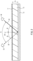
- the electromagnetic-wave shielding layer 3 of the electromagnetic-wave absorbing sheet according to the present embodiment is a member that is arranged on the side opposite to the electromagnetic-wave absorbing sheet via the dielectric layer 2, and that reflects the electromagnetic waves that are incident from the resistance film 1.
- the electromagnetic-wave shielding layer 3 needs to have at least flexibility for conforming and curving when the electric resistance film 1 and the dielectric layer 2 curve, and light transmittance.
- a conductive lattice in which metal wires such as thin copper wires with a diameter of several tens to several hundreds of ⁇ m are arranged horizontally and vertically can be used as the electromagnetic-wave shielding layer 3.
- the electromagnetic-wave shielding layer 3 formed using the above-described mesh or conductive lattice is configured to have the minimal thickness at which it is possible to realize the surface electric resistance required for the electromagnetic-wave shielding layer in order to ensure flexibility and light transmittance. Also, if the fibers of the conductive mesh or the wires of the conductive lattice are damaged or cut, it is difficult to realize the desired surface electric resistance. For this reason, a reinforcement layer and protective layer formed using resin that is light-transmissive can be further formed on the rear surface side of the conductive lattice, and the electromagnetic-wave shielding layer 3 formed using a stacked body in which the electromagnetic-wave reflecting portion formed by the conductive material and a film forming portion made of resin are stacked can be used.
- the electromagnetic-wave absorbing sheet according to the present embodiment, by providing the adhesive layer 4, the electromagnetic-wave absorbing sheet, which is a stacked body obtained by stacking the electric resistance film 1, the dielectric layer 2, and the electromagnetic-wave shielding layer 3, can be adhered at a desired position, such as the inner surface of the housing storing the electrical circuit, or the inner surface or outer surface of an electrical device.
- the electromagnetic-wave absorbing sheet of the present embodiment is flexible, the electromagnetic-wave absorbing sheet can be easily adhered to a curved surface, and by providing the adhesive layer 4 on the rear surface, the ease of handling the electromagnetic-wave absorbing sheet improves.
- a known material used as an adhesive layer such as adhesive tape, an acrylic-based adhesive, a rubber-based adhesive, a silicone-based adhesive, or the like can be used as the adhesive layer 4.
- a tackifier or a cross-linking agent can also be used to adjust the tackiness to the adherend, and to reduce adhesive residue.
- the tackiness to the adherend is preferably 5 N/10 mm to 12 N/10 mm. If the tackiness is smaller than 5 N/10 mm, the electromagnetic-wave absorbing sheet will easily peel off of the adherend or shift in some cases. Also, if the tackiness is greater than 12 N/10 mm, the electromagnetic-wave absorbing sheet will be more difficult to peel off of the adherend.
- an adhesive layer 4 that adheres the electromagnetic-wave absorbing sheet to the adherend such that it cannot be peeled off can be used as the adhesive layer 4 used in the electromagnetic-wave absorbing sheet according to the present embodiment, and an adhesive layer 4 that performs peelable adhesion can also be used thereas.
- the configuration including the adhesive layer 4 is not an essential element, but the electromagnetic-wave absorbing sheet can be adhered to a desired member using various types of conventionally common adhesion methods.
- the protective layer 5 can be provided on the incident surface of the electromagnetic waves, which is the surface of the electric resistance film 1.
- the thickness of the protective layer 5 is preferably thinner within a range of being able to protect the electric resistance film 1. Specifically, the thickness of the protective layer 5 is preferably 150 ⁇ m or less, and more preferably 100 ⁇ m or less. If the thickness of the protective layer exceeds 150 ⁇ m, the electromagnetic-wave absorbing performance decreases and the electromagnetic-wave absorption amount falls below 20 dB in some cases. Also, since the overall thickness of the electromagnetic-wave absorbing sheet increases, flexibility decreases.
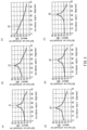
- the reflection attenuation amount is approximately 18 dB in the state in which the incidence angle ⁇ is equal to 0 degrees, which is perpendicular incidence, the reflection attenuation amount increases when the incidence angle increases, the reflection attenuation amount is 20 dB when the incidence angle ⁇ is 5 degrees, and the reflection attenuation amount reaches approximately 45 dB, which is the peak, when the incidence angle ⁇ is 34 degrees.
- the reflection attenuation amount decreases as the incidence angle ⁇ increases, and the reflection attenuation amount reaches 20 dB when the incidence angle ⁇ is 55 degrees. According to this result, with the sheet 1, it is understood that even if the electromagnetic waves are incident at incidence angles having a 50-degree incidence angle range between incidence angles ⁇ of 5 degrees and 55 degrees, a high reflection attenuation amount of 20 dB or more can be maintained. Also, in the sheet 1, it is understood that the surface electric resistance of the electric resistance film 1 is subjected to impedance matching at 310 ⁇ /sq with respect to electromagnetic waves with an incidence angle ⁇ of 34 degrees.
- the sheet 5 it is understood that even if the electromagnetic waves are incident at incidence angles having a 53-degree incidence angle range between incidence angles ⁇ of 3 degrees and 56 degrees, a high reflection attenuation amount of 20 dB or more can be maintained. Also, in the sheet 5, it is understood that the surface electric resistance of the electric resistance film 1 has been impedance-matched at 465 ⁇ /sq with respect to the electromagnetic waves with an incidence angle ⁇ of 37.5 degrees.
- the reflection attenuation amount is approximately 19 dB when the incidence angle ⁇ is equal to 0 degrees, which is perpendicular incidence, the reflection attenuation amount increases when the incidence angle increases, the reflection attenuation amount is 20 dB when the incidence angle ⁇ is 3 degrees, the reflection attenuation amount reaches a peak value of approximately 51 dB when the incidence angle ⁇ is 43 degrees, and thereafter the reflection attenuation amount decreases and reaches 20 dB when the incidence angle ⁇ is 53 degrees.
- the sheet 6 it is possible to maintain a reflection attenuation amount of 20 dB or more with respect to electromagnetic waves in a 50-degree incidence angle range in which the incidence angle ⁇ is 3 to 53 degrees. Also, with the sheet 6, it is indicated that the surface electric resistance of the electric resistance film 1 is impedance-matched at 500 ⁇ /sq.
- the reflection attenuation amount can be maintained at 20 dB or more, even if the range of the incidence angles ⁇ is 40 or 50 degrees in ranges in which the surface electric resistance of the electric resistance film that reaches the input impedance in the space is less than and greater than 377 ⁇ /sq. Since the reflection attenuation amount being 20 dB means that 99% of the electromagnetic waves will be absorbed, it can be determined that the electromagnetic-wave absorbing properties are sufficient in practical applications.
- the surface electric resistance of the electric resistance film 1 is 310 ⁇ /sq or more and 345 ⁇ /sq or less, or in a range in which the surface electric resistance is 420 ⁇ /sq or more and 500 ⁇ /sq or less, it is possible to ensure a reflection attenuation amount of-20 dB or more in a range of incidence angles ⁇ of up to 50 degrees.
- the optical property of the electromagnetic-wave absorbing sheet according to the present embodiment was within a preferable numeric value range in which the total light transmittance was 30% or more and the haze value was 40 or less.
- the electric resistance film that is arranged on the surface on the side of the electromagnetic-wave absorbing sheet according to the present embodiment on which the electromagnetic waves to be absorbed are incident is constituted by a conductive organic polymer, and thus the electromagnetic-wave absorbing properties can be maintained even if the electromagnetic-wave absorbing sheet is strongly bent. For this reason, it is possible to realize an electromagnetic-wave absorbing sheet that exhibits stable high electromagnetic-wave absorbing properties and is flexible and light-transmissive.
- the electromagnetic-wave absorbing sheet can be suitably used in a situation in which it is required that an interior or exterior is made visible while undesired electromagnetic waves are absorbed and not allowed to pass through, as with a living room curtain put in an electromagnetic-wave shielding state.
- the surface electric resistance of the electric resistance film is 303 ⁇ /sq or more and 350 ⁇ /sq or less, or to 415 ⁇ /sq or more and 502 ⁇ /sq or less, it is possible to, at a low cost, obtain electromagnetic-wave absorbing properties in which the reflection attenuation amount is 20 dB or more, which is thought to be sufficient for practical applications, even if the incidence angle range of the electromagnetic waves on the electromagnetic-wave absorbing sheet changes in a range of up to 40 degrees.
- an electromagnetic-wave absorbing sheet having electromagnetic-wave absorbing properties that are sufficient in practical applications with respect to electromagnetic waves incident in a wide angle range can be realized as an electromagnetic-wave absorbing sheet that is not light-transmissive.
- a wider range of materials for implementing the electromagnetic-wave absorbing sheet disclosed in the present application can be selected, such as using a lower-cost material that is not light-transmissive as the materials forming the electric resistance film and the dielectric layer instead of the constituent members of the layers included in the above-described electromagnetic-wave absorbing layers.
- a low-cost member such as aluminum foil can be employed as the electromagnetic-wave shielding layer as well.
Landscapes
- Engineering & Computer Science (AREA)
- Microelectronics & Electronic Packaging (AREA)
- Ceramic Engineering (AREA)
- Physics & Mathematics (AREA)
- Electromagnetism (AREA)
- Textile Engineering (AREA)
- Chemical & Material Sciences (AREA)
- Laminated Bodies (AREA)
- Shielding Devices Or Components To Electric Or Magnetic Fields (AREA)
Claims (6)
- Elektromagnetische-Wellen-absorbierende Folie, gebildet durch Stapeln eines Elektrischer-Widerstand-Films (1), einer dielektrischen Schicht (2) und einer elektromagnetische Wellen abschirmenden Schicht (3), wobei der Elektrischer-Widerstand-Film (1) unter Verwendung eines leitfähigen organischen Polymers gebildet ist und einen elektrischen Oberflächenwiderstand von 303 Ω/sq oder mehr und 350 Ω/sq oder weniger, oder von 415 Ω/sq oder mehr und 502 Ω/sq oder weniger aufweist,
und dadurch gekennzeichnet, dass die dielektrische Schicht (2) unter Verwendung von Silicon-OCA gebildet ist. - Elektromagnetische-Wellen-absorbierende Folie gemäß Anspruch 1, wobei der Elektrischer-Widerstand-Film (1) einen elektrischen Oberflächenwiderstand von 310 Ω/sq oder mehr und 345 Ω/sq oder weniger, oder 420 Ω/sq oder mehr und 500 Ω/sq oder weniger aufweist.
- Elektromagnetische-Wellen-absorbierende Folie gemäß Anspruch 1 oder 2, wobei der Elektrischer-Widerstand-Film (1), die dielektrische Schicht (2) und die elektromagnetische Wellen abschirmende Schicht (3) alle lichtdurchlässig sind und die Folie insgesamt-lichtdurchlässig-ist.
- Elektromagnetische-Wellen-absorbierende Folie gemäß einem der Ansprüche 1 bis 3, wobei der Elektrischer-Widerstand-Film Poly(3,4-ethylendioxythiophen), Polystyrensulfonsäure und Polyvinylidenfluorid beinhaltet.
- Elektromagnetische-Wellen-absorbierende Folie gemäß Anspruch 4, wobei der Elektrischer-Widerstand-Film (1) ferner wasserlöslichen-Polyester beinhaltet.
- Elektromagnetische-Wellen-absorbierende Folie gemäß einem der Ansprüche 1 bis 5, wobei die dielektrische Schicht (2) auf eine Schichtdicke eingestellt ist, bei welcher es ermöglicht ist, elektromagnetische Wellen in einem Hochfrequenzband in oder über einem Millimeterwellenband zu absorbieren.
Applications Claiming Priority (2)
| Application Number | Priority Date | Filing Date | Title |
|---|---|---|---|
| JP2017176000 | 2017-09-13 | ||
| PCT/JP2018/033662 WO2019054378A1 (ja) | 2017-09-13 | 2018-09-11 | 電磁波吸収シート |
Publications (5)
| Publication Number | Publication Date |
|---|---|
| EP3684155A1 EP3684155A1 (de) | 2020-07-22 |
| EP3684155A4 EP3684155A4 (de) | 2021-06-09 |
| EP3684155C0 EP3684155C0 (de) | 2024-04-03 |
| EP3684155B1 EP3684155B1 (de) | 2024-04-03 |
| EP3684155B9 true EP3684155B9 (de) | 2024-07-03 |
Family
ID=65722640
Family Applications (1)
| Application Number | Title | Priority Date | Filing Date |
|---|---|---|---|
| EP18856761.4A Active EP3684155B9 (de) | 2017-09-13 | 2018-09-11 | Folie zum absorbieren elektromagnetischer wellen |
Country Status (5)
| Country | Link |
|---|---|
| US (1) | US20210144890A1 (de) |
| EP (1) | EP3684155B9 (de) |
| JP (1) | JPWO2019054378A1 (de) |
| TW (1) | TWI771486B (de) |
| WO (1) | WO2019054378A1 (de) |
Families Citing this family (5)
| Publication number | Priority date | Publication date | Assignee | Title |
|---|---|---|---|---|
| JP7296955B2 (ja) * | 2018-06-07 | 2023-06-23 | マクセル株式会社 | 電磁波吸収シート |
| JP7479124B2 (ja) * | 2019-03-29 | 2024-05-08 | Toppanホールディングス株式会社 | 電磁波抑制シート及びその製造方法 |
| JP7479811B2 (ja) * | 2019-09-25 | 2024-05-09 | 積水化学工業株式会社 | λ/4型電波吸収体 |
| CN111695217B (zh) * | 2020-06-09 | 2021-12-28 | 西安交通大学 | 一种基于增材制造的宽角度吸波结构设计方法 |
| CN114236201B (zh) * | 2021-12-02 | 2023-02-17 | 浙江大学 | 一种频率可重构全角度完美匹配吸波暗室 |
Family Cites Families (13)
| Publication number | Priority date | Publication date | Assignee | Title |
|---|---|---|---|---|
| JPH05335832A (ja) | 1991-12-24 | 1993-12-17 | Tdk Corp | 電波吸収体 |
| JPH08307088A (ja) * | 1995-04-27 | 1996-11-22 | C I Kasei Co Ltd | 電波吸収体 |
| JPH09232787A (ja) | 1996-02-27 | 1997-09-05 | Tosoh Corp | 電波吸収体 |
| JP2000059066A (ja) * | 1998-08-10 | 2000-02-25 | Mitsubishi Chemicals Corp | 電波吸収体 |
| JP4435659B2 (ja) | 2004-09-17 | 2010-03-24 | 三菱電線工業株式会社 | 電波吸収体 |
| JP2008135485A (ja) | 2006-11-27 | 2008-06-12 | Taika:Kk | 電波吸収体およびその製造方法 |
| JP5554578B2 (ja) * | 2010-01-26 | 2014-07-23 | 帝人デュポンフィルム株式会社 | 導電性フィルム |
| TWI501866B (zh) * | 2013-09-02 | 2015-10-01 | Nat Inst Chung Shan Science & Technology | Conductive polymer broadband microwave absorbing body |
| JP2015173010A (ja) * | 2014-03-11 | 2015-10-01 | 日立マクセル株式会社 | 透明導電パターンの製造方法及び透明導電性シート |
| JP6184579B2 (ja) * | 2015-12-14 | 2017-08-23 | 日東電工株式会社 | 電磁波吸収体およびそれを備えた電磁波吸収体付成形体 |
| JP6375403B2 (ja) * | 2016-03-04 | 2018-08-15 | 日東電工株式会社 | 電磁波吸収体および電磁波吸収体付成形品 |
| WO2018088492A1 (ja) * | 2016-11-10 | 2018-05-17 | マクセルホールディングス株式会社 | 電磁波吸収シート |
| EP3595422B1 (de) * | 2017-03-10 | 2024-11-27 | Maxell, Ltd. | Folie zum absorbieren elektromagnetischer wellen |
-
2018
- 2018-09-11 US US16/620,778 patent/US20210144890A1/en not_active Abandoned
- 2018-09-11 WO PCT/JP2018/033662 patent/WO2019054378A1/ja not_active Ceased
- 2018-09-11 EP EP18856761.4A patent/EP3684155B9/de active Active
- 2018-09-11 JP JP2019542069A patent/JPWO2019054378A1/ja active Pending
- 2018-09-11 TW TW107131672A patent/TWI771486B/zh active
Also Published As
| Publication number | Publication date |
|---|---|
| WO2019054378A1 (ja) | 2019-03-21 |
| EP3684155A4 (de) | 2021-06-09 |
| EP3684155C0 (de) | 2024-04-03 |
| EP3684155B1 (de) | 2024-04-03 |
| TWI771486B (zh) | 2022-07-21 |
| TW201919893A (zh) | 2019-06-01 |
| EP3684155A1 (de) | 2020-07-22 |
| JPWO2019054378A1 (ja) | 2020-08-27 |
| US20210144890A1 (en) | 2021-05-13 |
Similar Documents
| Publication | Publication Date | Title |
|---|---|---|
| JP7591103B2 (ja) | 電磁波吸収シート | |
| CN110169218B (zh) | 电磁波吸收片 | |
| EP3684155B9 (de) | Folie zum absorbieren elektromagnetischer wellen | |
| JP7296955B2 (ja) | 電磁波吸収シート | |
| JP7141546B2 (ja) | 測定システム、および電波遮蔽部 | |
| US12349328B2 (en) | Electric-wave absorber and manufacturing method for electric-wave absorber | |
| JP7687903B2 (ja) | 電波吸収体、および電波吸収体の製造方法 | |
| JPWO2022158562A5 (de) | ||
| WO2025105332A1 (ja) | 電磁波吸収シート |
Legal Events
| Date | Code | Title | Description |
|---|---|---|---|
| STAA | Information on the status of an ep patent application or granted ep patent |
Free format text: STATUS: THE INTERNATIONAL PUBLICATION HAS BEEN MADE |
|
| PUAI | Public reference made under article 153(3) epc to a published international application that has entered the european phase |
Free format text: ORIGINAL CODE: 0009012 |
|
| STAA | Information on the status of an ep patent application or granted ep patent |
Free format text: STATUS: REQUEST FOR EXAMINATION WAS MADE |
|
| 17P | Request for examination filed |
Effective date: 20191209 |
|
| AK | Designated contracting states |
Kind code of ref document: A1 Designated state(s): AL AT BE BG CH CY CZ DE DK EE ES FI FR GB GR HR HU IE IS IT LI LT LU LV MC MK MT NL NO PL PT RO RS SE SI SK SM TR |
|
| AX | Request for extension of the european patent |
Extension state: BA ME |
|
| DAV | Request for validation of the european patent (deleted) | ||
| DAX | Request for extension of the european patent (deleted) | ||
| A4 | Supplementary search report drawn up and despatched |
Effective date: 20210507 |
|
| RIC1 | Information provided on ipc code assigned before grant |
Ipc: H05K 9/00 20060101AFI20210430BHEP Ipc: B32B 7/02 20190101ALI20210430BHEP Ipc: B32B 27/00 20060101ALI20210430BHEP |
|
| RAP3 | Party data changed (applicant data changed or rights of an application transferred) |
Owner name: MAXELL, LTD. |
|
| GRAP | Despatch of communication of intention to grant a patent |
Free format text: ORIGINAL CODE: EPIDOSNIGR1 |
|
| STAA | Information on the status of an ep patent application or granted ep patent |
Free format text: STATUS: GRANT OF PATENT IS INTENDED |
|
| INTG | Intention to grant announced |
Effective date: 20231017 |
|
| GRAS | Grant fee paid |
Free format text: ORIGINAL CODE: EPIDOSNIGR3 |
|
| GRAA | (expected) grant |
Free format text: ORIGINAL CODE: 0009210 |
|
| STAA | Information on the status of an ep patent application or granted ep patent |
Free format text: STATUS: THE PATENT HAS BEEN GRANTED |
|
| AK | Designated contracting states |
Kind code of ref document: B1 Designated state(s): AL AT BE BG CH CY CZ DE DK EE ES FI FR GB GR HR HU IE IS IT LI LT LU LV MC MK MT NL NO PL PT RO RS SE SI SK SM TR |
|
| REG | Reference to a national code |
Ref country code: GB Ref legal event code: FG4D |
|
| REG | Reference to a national code |
Ref country code: CH Ref legal event code: EP |
|
| REG | Reference to a national code |
Ref country code: IE Ref legal event code: FG4D |
|
| REG | Reference to a national code |
Ref country code: DE Ref legal event code: R096 Ref document number: 602018067644 Country of ref document: DE |
|
| U01 | Request for unitary effect filed |
Effective date: 20240426 |
|
| U07 | Unitary effect registered |
Designated state(s): AT BE BG DE DK EE FI FR IT LT LU LV MT NL PT SE SI Effective date: 20240506 |
|
| REG | Reference to a national code |
Ref country code: CH Ref legal event code: PK Free format text: BERICHTIGUNG B9 |
|
| PG25 | Lapsed in a contracting state [announced via postgrant information from national office to epo] |
Ref country code: IS Free format text: LAPSE BECAUSE OF FAILURE TO SUBMIT A TRANSLATION OF THE DESCRIPTION OR TO PAY THE FEE WITHIN THE PRESCRIBED TIME-LIMIT Effective date: 20240803 |
|
| PG25 | Lapsed in a contracting state [announced via postgrant information from national office to epo] |
Ref country code: HR Free format text: LAPSE BECAUSE OF FAILURE TO SUBMIT A TRANSLATION OF THE DESCRIPTION OR TO PAY THE FEE WITHIN THE PRESCRIBED TIME-LIMIT Effective date: 20240403 |
|
| PG25 | Lapsed in a contracting state [announced via postgrant information from national office to epo] |
Ref country code: GR Free format text: LAPSE BECAUSE OF FAILURE TO SUBMIT A TRANSLATION OF THE DESCRIPTION OR TO PAY THE FEE WITHIN THE PRESCRIBED TIME-LIMIT Effective date: 20240704 |
|
| PG25 | Lapsed in a contracting state [announced via postgrant information from national office to epo] |
Ref country code: ES Free format text: LAPSE BECAUSE OF FAILURE TO SUBMIT A TRANSLATION OF THE DESCRIPTION OR TO PAY THE FEE WITHIN THE PRESCRIBED TIME-LIMIT Effective date: 20240403 |
|
| PG25 | Lapsed in a contracting state [announced via postgrant information from national office to epo] |
Ref country code: CZ Free format text: LAPSE BECAUSE OF FAILURE TO SUBMIT A TRANSLATION OF THE DESCRIPTION OR TO PAY THE FEE WITHIN THE PRESCRIBED TIME-LIMIT Effective date: 20240403 |
|
| PG25 | Lapsed in a contracting state [announced via postgrant information from national office to epo] |
Ref country code: PL Free format text: LAPSE BECAUSE OF FAILURE TO SUBMIT A TRANSLATION OF THE DESCRIPTION OR TO PAY THE FEE WITHIN THE PRESCRIBED TIME-LIMIT Effective date: 20240403 |
|
| U20 | Renewal fee for the european patent with unitary effect paid |
Year of fee payment: 7 Effective date: 20240925 |
|
| PG25 | Lapsed in a contracting state [announced via postgrant information from national office to epo] |
Ref country code: PL Free format text: LAPSE BECAUSE OF FAILURE TO SUBMIT A TRANSLATION OF THE DESCRIPTION OR TO PAY THE FEE WITHIN THE PRESCRIBED TIME-LIMIT Effective date: 20240403 Ref country code: IS Free format text: LAPSE BECAUSE OF FAILURE TO SUBMIT A TRANSLATION OF THE DESCRIPTION OR TO PAY THE FEE WITHIN THE PRESCRIBED TIME-LIMIT Effective date: 20240803 Ref country code: HR Free format text: LAPSE BECAUSE OF FAILURE TO SUBMIT A TRANSLATION OF THE DESCRIPTION OR TO PAY THE FEE WITHIN THE PRESCRIBED TIME-LIMIT Effective date: 20240403 Ref country code: GR Free format text: LAPSE BECAUSE OF FAILURE TO SUBMIT A TRANSLATION OF THE DESCRIPTION OR TO PAY THE FEE WITHIN THE PRESCRIBED TIME-LIMIT Effective date: 20240704 Ref country code: ES Free format text: LAPSE BECAUSE OF FAILURE TO SUBMIT A TRANSLATION OF THE DESCRIPTION OR TO PAY THE FEE WITHIN THE PRESCRIBED TIME-LIMIT Effective date: 20240403 Ref country code: CZ Free format text: LAPSE BECAUSE OF FAILURE TO SUBMIT A TRANSLATION OF THE DESCRIPTION OR TO PAY THE FEE WITHIN THE PRESCRIBED TIME-LIMIT Effective date: 20240403 Ref country code: RS Free format text: LAPSE BECAUSE OF FAILURE TO SUBMIT A TRANSLATION OF THE DESCRIPTION OR TO PAY THE FEE WITHIN THE PRESCRIBED TIME-LIMIT Effective date: 20240703 |
|
| REG | Reference to a national code |
Ref country code: DE Ref legal event code: R097 Ref document number: 602018067644 Country of ref document: DE |
|
| PG25 | Lapsed in a contracting state [announced via postgrant information from national office to epo] |
Ref country code: RO Free format text: LAPSE BECAUSE OF FAILURE TO SUBMIT A TRANSLATION OF THE DESCRIPTION OR TO PAY THE FEE WITHIN THE PRESCRIBED TIME-LIMIT Effective date: 20240403 Ref country code: SK Free format text: LAPSE BECAUSE OF FAILURE TO SUBMIT A TRANSLATION OF THE DESCRIPTION OR TO PAY THE FEE WITHIN THE PRESCRIBED TIME-LIMIT Effective date: 20240403 |
|
| PG25 | Lapsed in a contracting state [announced via postgrant information from national office to epo] |
Ref country code: SM Free format text: LAPSE BECAUSE OF FAILURE TO SUBMIT A TRANSLATION OF THE DESCRIPTION OR TO PAY THE FEE WITHIN THE PRESCRIBED TIME-LIMIT Effective date: 20240403 |
|
| PG25 | Lapsed in a contracting state [announced via postgrant information from national office to epo] |
Ref country code: SM Free format text: LAPSE BECAUSE OF FAILURE TO SUBMIT A TRANSLATION OF THE DESCRIPTION OR TO PAY THE FEE WITHIN THE PRESCRIBED TIME-LIMIT Effective date: 20240403 Ref country code: SK Free format text: LAPSE BECAUSE OF FAILURE TO SUBMIT A TRANSLATION OF THE DESCRIPTION OR TO PAY THE FEE WITHIN THE PRESCRIBED TIME-LIMIT Effective date: 20240403 Ref country code: RO Free format text: LAPSE BECAUSE OF FAILURE TO SUBMIT A TRANSLATION OF THE DESCRIPTION OR TO PAY THE FEE WITHIN THE PRESCRIBED TIME-LIMIT Effective date: 20240403 |
|
| PLBE | No opposition filed within time limit |
Free format text: ORIGINAL CODE: 0009261 |
|
| STAA | Information on the status of an ep patent application or granted ep patent |
Free format text: STATUS: NO OPPOSITION FILED WITHIN TIME LIMIT |
|
| 26N | No opposition filed |
Effective date: 20250106 |
|
| PG25 | Lapsed in a contracting state [announced via postgrant information from national office to epo] |
Ref country code: MC Free format text: LAPSE BECAUSE OF FAILURE TO SUBMIT A TRANSLATION OF THE DESCRIPTION OR TO PAY THE FEE WITHIN THE PRESCRIBED TIME-LIMIT Effective date: 20240403 |
|
| REG | Reference to a national code |
Ref country code: CH Ref legal event code: PL |
|
| PG25 | Lapsed in a contracting state [announced via postgrant information from national office to epo] |
Ref country code: CH Free format text: LAPSE BECAUSE OF NON-PAYMENT OF DUE FEES Effective date: 20240930 |
|
| PG25 | Lapsed in a contracting state [announced via postgrant information from national office to epo] |
Ref country code: IE Free format text: LAPSE BECAUSE OF NON-PAYMENT OF DUE FEES Effective date: 20240911 |
|
| PGFP | Annual fee paid to national office [announced via postgrant information from national office to epo] |
Ref country code: NO Payment date: 20250923 Year of fee payment: 8 |
|
| PGFP | Annual fee paid to national office [announced via postgrant information from national office to epo] |
Ref country code: GB Payment date: 20250919 Year of fee payment: 8 |
|
| U20 | Renewal fee for the european patent with unitary effect paid |
Year of fee payment: 8 Effective date: 20250924 |
|
| PG25 | Lapsed in a contracting state [announced via postgrant information from national office to epo] |
Ref country code: CY Free format text: LAPSE BECAUSE OF FAILURE TO SUBMIT A TRANSLATION OF THE DESCRIPTION OR TO PAY THE FEE WITHIN THE PRESCRIBED TIME-LIMIT; INVALID AB INITIO Effective date: 20180911 |
|
| PG25 | Lapsed in a contracting state [announced via postgrant information from national office to epo] |
Ref country code: HU Free format text: LAPSE BECAUSE OF FAILURE TO SUBMIT A TRANSLATION OF THE DESCRIPTION OR TO PAY THE FEE WITHIN THE PRESCRIBED TIME-LIMIT; INVALID AB INITIO Effective date: 20180911 |