EP3684146A1 - Circuit board - Google Patents
Circuit board Download PDFInfo
- Publication number
- EP3684146A1 EP3684146A1 EP18856760.6A EP18856760A EP3684146A1 EP 3684146 A1 EP3684146 A1 EP 3684146A1 EP 18856760 A EP18856760 A EP 18856760A EP 3684146 A1 EP3684146 A1 EP 3684146A1
- Authority
- EP
- European Patent Office
- Prior art keywords
- resin layer
- circuit board
- layer
- group
- laminate
- Prior art date
- Legal status (The legal status is an assumption and is not a legal conclusion. Google has not performed a legal analysis and makes no representation as to the accuracy of the status listed.)
- Pending
Links
- 229920005989 resin Polymers 0.000 claims abstract description 223
- 239000011347 resin Substances 0.000 claims abstract description 223
- 229910052751 metal Inorganic materials 0.000 claims abstract description 103
- 239000002184 metal Substances 0.000 claims abstract description 103
- 230000005540 biological transmission Effects 0.000 abstract description 14
- 239000010410 layer Substances 0.000 description 338
- RYGMFSIKBFXOCR-UHFFFAOYSA-N Copper Chemical compound [Cu] RYGMFSIKBFXOCR-UHFFFAOYSA-N 0.000 description 43
- 239000000203 mixture Substances 0.000 description 34
- 239000011889 copper foil Substances 0.000 description 31
- 238000010438 heat treatment Methods 0.000 description 31
- OKKJLVBELUTLKV-UHFFFAOYSA-N Methanol Chemical compound OC OKKJLVBELUTLKV-UHFFFAOYSA-N 0.000 description 30
- 239000000758 substrate Substances 0.000 description 29
- 229920000642 polymer Polymers 0.000 description 28
- 230000003746 surface roughness Effects 0.000 description 27
- 238000004519 manufacturing process Methods 0.000 description 26
- 238000000034 method Methods 0.000 description 26
- SECXISVLQFMRJM-UHFFFAOYSA-N N-Methylpyrrolidone Chemical compound CN1CCCC1=O SECXISVLQFMRJM-UHFFFAOYSA-N 0.000 description 24
- 150000001875 compounds Chemical class 0.000 description 21
- 238000001914 filtration Methods 0.000 description 15
- 230000009477 glass transition Effects 0.000 description 15
- 239000002904 solvent Substances 0.000 description 15
- 230000015572 biosynthetic process Effects 0.000 description 14
- 238000003786 synthesis reaction Methods 0.000 description 14
- 238000011156 evaluation Methods 0.000 description 13
- 125000004432 carbon atom Chemical group C* 0.000 description 12
- 229910052802 copper Inorganic materials 0.000 description 12
- 239000010949 copper Substances 0.000 description 12
- -1 neopentylene group Chemical group 0.000 description 12
- 229920002799 BoPET Polymers 0.000 description 11
- 239000011888 foil Substances 0.000 description 11
- 238000006243 chemical reaction Methods 0.000 description 10
- BWHMMNNQKKPAPP-UHFFFAOYSA-L potassium carbonate Chemical compound [K+].[K+].[O-]C([O-])=O BWHMMNNQKKPAPP-UHFFFAOYSA-L 0.000 description 10
- 239000000126 substance Substances 0.000 description 10
- 150000002430 hydrocarbons Chemical group 0.000 description 9
- 238000011282 treatment Methods 0.000 description 9
- 239000012790 adhesive layer Substances 0.000 description 8
- 238000005530 etching Methods 0.000 description 8
- 238000005065 mining Methods 0.000 description 8
- 150000003839 salts Chemical class 0.000 description 8
- 239000000243 solution Substances 0.000 description 8
- 239000004593 Epoxy Substances 0.000 description 7
- 239000000853 adhesive Substances 0.000 description 7
- 230000001070 adhesive effect Effects 0.000 description 7
- YMWUJEATGCHHMB-UHFFFAOYSA-N Dichloromethane Chemical compound ClCCl YMWUJEATGCHHMB-UHFFFAOYSA-N 0.000 description 6
- 238000000576 coating method Methods 0.000 description 6
- BGTOWKSIORTVQH-UHFFFAOYSA-N cyclopentanone Chemical compound O=C1CCCC1 BGTOWKSIORTVQH-UHFFFAOYSA-N 0.000 description 6
- 238000003825 pressing Methods 0.000 description 6
- 238000012360 testing method Methods 0.000 description 6
- UMPGNGRIGSEMTC-UHFFFAOYSA-N 4-[1-(4-hydroxyphenyl)-3,3,5-trimethylcyclohexyl]phenol Chemical compound C1C(C)CC(C)(C)CC1(C=1C=CC(O)=CC=1)C1=CC=C(O)C=C1 UMPGNGRIGSEMTC-UHFFFAOYSA-N 0.000 description 5
- 238000000137 annealing Methods 0.000 description 5
- 125000002029 aromatic hydrocarbon group Chemical group 0.000 description 5
- 125000005843 halogen group Chemical group 0.000 description 5
- 238000003475 lamination Methods 0.000 description 5
- 238000005259 measurement Methods 0.000 description 5
- 239000012299 nitrogen atmosphere Substances 0.000 description 5
- 229910000027 potassium carbonate Inorganic materials 0.000 description 5
- 238000011084 recovery Methods 0.000 description 5
- 239000007787 solid Substances 0.000 description 5
- 239000011248 coating agent Substances 0.000 description 4
- 230000000052 comparative effect Effects 0.000 description 4
- 125000004093 cyano group Chemical group *C#N 0.000 description 4
- 125000000392 cycloalkenyl group Chemical group 0.000 description 4
- 125000000753 cycloalkyl group Chemical group 0.000 description 4
- 238000010790 dilution Methods 0.000 description 4
- 239000012895 dilution Substances 0.000 description 4
- 125000002950 monocyclic group Chemical group 0.000 description 4
- 125000000449 nitro group Chemical group [O-][N+](*)=O 0.000 description 4
- 125000003367 polycyclic group Chemical group 0.000 description 4
- 125000001302 tertiary amino group Chemical group 0.000 description 4
- ZWEHNKRNPOVVGH-UHFFFAOYSA-N 2-Butanone Chemical compound CCC(C)=O ZWEHNKRNPOVVGH-UHFFFAOYSA-N 0.000 description 3
- UHOVQNZJYSORNB-UHFFFAOYSA-N Benzene Chemical compound C1=CC=CC=C1 UHOVQNZJYSORNB-UHFFFAOYSA-N 0.000 description 3
- NRFQZTCQAYEXEE-UHFFFAOYSA-N Fenclorim Chemical compound ClC1=CC(Cl)=NC(C=2C=CC=CC=2)=N1 NRFQZTCQAYEXEE-UHFFFAOYSA-N 0.000 description 3
- ZMXDDKWLCZADIW-UHFFFAOYSA-N N,N-Dimethylformamide Chemical compound CN(C)C=O ZMXDDKWLCZADIW-UHFFFAOYSA-N 0.000 description 3
- 239000004642 Polyimide Substances 0.000 description 3
- YXFVVABEGXRONW-UHFFFAOYSA-N Toluene Chemical compound CC1=CC=CC=C1 YXFVVABEGXRONW-UHFFFAOYSA-N 0.000 description 3
- 239000000654 additive Substances 0.000 description 3
- 125000002723 alicyclic group Chemical group 0.000 description 3
- 229910052801 chlorine Inorganic materials 0.000 description 3
- 125000001309 chloro group Chemical group Cl* 0.000 description 3
- 239000004643 cyanate ester Chemical class 0.000 description 3
- 238000007772 electroless plating Methods 0.000 description 3
- 238000005516 engineering process Methods 0.000 description 3
- 229910052731 fluorine Inorganic materials 0.000 description 3
- 125000001153 fluoro group Chemical group F* 0.000 description 3
- 150000008282 halocarbons Chemical group 0.000 description 3
- 239000012212 insulator Substances 0.000 description 3
- 238000010030 laminating Methods 0.000 description 3
- 239000000463 material Substances 0.000 description 3
- 239000000178 monomer Substances 0.000 description 3
- 125000000962 organic group Chemical group 0.000 description 3
- 125000001997 phenyl group Chemical group [H]C1=C([H])C([H])=C(*)C([H])=C1[H] 0.000 description 3
- 229920001721 polyimide Polymers 0.000 description 3
- 229920001296 polysiloxane Chemical class 0.000 description 3
- 239000000523 sample Substances 0.000 description 3
- JDIPZHAYUYYGSN-UHFFFAOYSA-N (4-propylphenyl) cyanate Chemical compound CCCC1=CC=C(OC#N)C=C1 JDIPZHAYUYYGSN-UHFFFAOYSA-N 0.000 description 2
- FBHPRUXJQNWTEW-UHFFFAOYSA-N 1-benzyl-2-methylimidazole Chemical compound CC1=NC=CN1CC1=CC=CC=C1 FBHPRUXJQNWTEW-UHFFFAOYSA-N 0.000 description 2
- ARXJGSRGQADJSQ-UHFFFAOYSA-N 1-methoxypropan-2-ol Chemical compound COCC(C)O ARXJGSRGQADJSQ-UHFFFAOYSA-N 0.000 description 2
- 125000000094 2-phenylethyl group Chemical group [H]C1=C([H])C([H])=C(C([H])=C1[H])C([H])([H])C([H])([H])* 0.000 description 2
- YEJRWHAVMIAJKC-UHFFFAOYSA-N 4-Butyrolactone Chemical compound O=C1CCCO1 YEJRWHAVMIAJKC-UHFFFAOYSA-N 0.000 description 2
- OUKOUEHLRVEKCJ-UHFFFAOYSA-N 4-[1-(4-hydroxyphenyl)nonyl]phenol Chemical compound C=1C=C(O)C=CC=1C(CCCCCCCC)C1=CC=C(O)C=C1 OUKOUEHLRVEKCJ-UHFFFAOYSA-N 0.000 description 2
- ZCYVEMRRCGMTRW-UHFFFAOYSA-N 7553-56-2 Chemical group [I] ZCYVEMRRCGMTRW-UHFFFAOYSA-N 0.000 description 2
- WKBOTKDWSSQWDR-UHFFFAOYSA-N Bromine atom Chemical group [Br] WKBOTKDWSSQWDR-UHFFFAOYSA-N 0.000 description 2
- OKTJSMMVPCPJKN-UHFFFAOYSA-N Carbon Chemical compound [C] OKTJSMMVPCPJKN-UHFFFAOYSA-N 0.000 description 2
- CURLTUGMZLYLDI-UHFFFAOYSA-N Carbon dioxide Chemical compound O=C=O CURLTUGMZLYLDI-UHFFFAOYSA-N 0.000 description 2
- IAZDPXIOMUYVGZ-UHFFFAOYSA-N Dimethylsulphoxide Chemical compound CS(C)=O IAZDPXIOMUYVGZ-UHFFFAOYSA-N 0.000 description 2
- 125000005073 adamantyl group Chemical group C12(CC3CC(CC(C1)C3)C2)* 0.000 description 2
- 125000003545 alkoxy group Chemical group 0.000 description 2
- 125000005428 anthryl group Chemical group [H]C1=C([H])C([H])=C2C([H])=C3C(*)=C([H])C([H])=C([H])C3=C([H])C2=C1[H] 0.000 description 2
- 239000003963 antioxidant agent Substances 0.000 description 2
- 125000003710 aryl alkyl group Chemical group 0.000 description 2
- 125000003118 aryl group Chemical group 0.000 description 2
- 125000001797 benzyl group Chemical group [H]C1=C([H])C([H])=C(C([H])=C1[H])C([H])([H])* 0.000 description 2
- IISBACLAFKSPIT-UHFFFAOYSA-N bisphenol A Chemical compound C=1C=C(O)C=CC=1C(C)(C)C1=CC=C(O)C=C1 IISBACLAFKSPIT-UHFFFAOYSA-N 0.000 description 2
- 229910052799 carbon Inorganic materials 0.000 description 2
- 239000003795 chemical substances by application Substances 0.000 description 2
- 230000006835 compression Effects 0.000 description 2
- 238000007906 compression Methods 0.000 description 2
- 239000004020 conductor Substances 0.000 description 2
- 125000001047 cyclobutenyl group Chemical group C1(=CCC1)* 0.000 description 2
- 125000001995 cyclobutyl group Chemical group [H]C1([H])C([H])([H])C([H])(*)C1([H])[H] 0.000 description 2
- JHIVVAPYMSGYDF-UHFFFAOYSA-N cyclohexanone Chemical compound O=C1CCCCC1 JHIVVAPYMSGYDF-UHFFFAOYSA-N 0.000 description 2
- 125000000596 cyclohexenyl group Chemical group C1(=CCCCC1)* 0.000 description 2
- 125000000113 cyclohexyl group Chemical group [H]C1([H])C([H])([H])C([H])([H])C([H])(*)C([H])([H])C1([H])[H] 0.000 description 2
- 125000002433 cyclopentenyl group Chemical group C1(=CCCC1)* 0.000 description 2
- 125000001511 cyclopentyl group Chemical group [H]C1([H])C([H])([H])C([H])([H])C([H])(*)C1([H])[H] 0.000 description 2
- 125000000298 cyclopropenyl group Chemical group [H]C1=C([H])C1([H])* 0.000 description 2
- 125000001559 cyclopropyl group Chemical group [H]C1([H])C([H])([H])C1([H])* 0.000 description 2
- 230000006866 deterioration Effects 0.000 description 2
- 238000011161 development Methods 0.000 description 2
- 238000010586 diagram Methods 0.000 description 2
- USIUVYZYUHIAEV-UHFFFAOYSA-N diphenyl ether Chemical compound C=1C=CC=CC=1OC1=CC=CC=C1 USIUVYZYUHIAEV-UHFFFAOYSA-N 0.000 description 2
- KZTYYGOKRVBIMI-UHFFFAOYSA-N diphenyl sulfone Chemical compound C=1C=CC=CC=1S(=O)(=O)C1=CC=CC=C1 KZTYYGOKRVBIMI-UHFFFAOYSA-N 0.000 description 2
- 238000009713 electroplating Methods 0.000 description 2
- 239000011521 glass Substances 0.000 description 2
- 229910052740 iodine Inorganic materials 0.000 description 2
- 125000002496 methyl group Chemical group [H]C([H])([H])* 0.000 description 2
- 125000001624 naphthyl group Chemical group 0.000 description 2
- 125000004923 naphthylmethyl group Chemical group C1(=CC=CC2=CC=CC=C12)C* 0.000 description 2
- 125000003518 norbornenyl group Chemical group C12(C=CC(CC1)C2)* 0.000 description 2
- 125000002868 norbornyl group Chemical group C12(CCC(CC1)C2)* 0.000 description 2
- 125000004344 phenylpropyl group Chemical group 0.000 description 2
- 229920000728 polyester Polymers 0.000 description 2
- 229920001955 polyphenylene ether Polymers 0.000 description 2
- 238000012545 processing Methods 0.000 description 2
- 230000005855 radiation Effects 0.000 description 2
- 238000004544 sputter deposition Methods 0.000 description 2
- HHVIBTZHLRERCL-UHFFFAOYSA-N sulfonyldimethane Chemical compound CS(C)(=O)=O HHVIBTZHLRERCL-UHFFFAOYSA-N 0.000 description 2
- 125000000999 tert-butyl group Chemical group [H]C([H])([H])C(*)(C([H])([H])[H])C([H])([H])[H] 0.000 description 2
- 229920001187 thermosetting polymer Polymers 0.000 description 2
- 125000003944 tolyl group Chemical group 0.000 description 2
- 125000000391 vinyl group Chemical group [H]C([*])=C([H])[H] 0.000 description 2
- 229920002554 vinyl polymer Polymers 0.000 description 2
- 125000005023 xylyl group Chemical group 0.000 description 2
- CYSGHNMQYZDMIA-UHFFFAOYSA-N 1,3-Dimethyl-2-imidazolidinon Chemical compound CN1CCN(C)C1=O CYSGHNMQYZDMIA-UHFFFAOYSA-N 0.000 description 1
- VXNZUUAINFGPBY-UHFFFAOYSA-N 1-Butene Chemical group CCC=C VXNZUUAINFGPBY-UHFFFAOYSA-N 0.000 description 1
- ZFPGARUNNKGOBB-UHFFFAOYSA-N 1-Ethyl-2-pyrrolidinone Chemical compound CCN1CCCC1=O ZFPGARUNNKGOBB-UHFFFAOYSA-N 0.000 description 1
- MBDUIEKYVPVZJH-UHFFFAOYSA-N 1-ethylsulfonylethane Chemical compound CCS(=O)(=O)CC MBDUIEKYVPVZJH-UHFFFAOYSA-N 0.000 description 1
- 150000003923 2,5-pyrrolediones Chemical class 0.000 description 1
- MEVBAGCIOOTPLF-UHFFFAOYSA-N 2-[[5-(oxiran-2-ylmethoxy)naphthalen-2-yl]oxymethyl]oxirane Chemical compound C1OC1COC(C=C1C=CC=2)=CC=C1C=2OCC1CO1 MEVBAGCIOOTPLF-UHFFFAOYSA-N 0.000 description 1
- ZDULHUHNYHJYKA-UHFFFAOYSA-N 2-propan-2-ylsulfonylpropane Chemical compound CC(C)S(=O)(=O)C(C)C ZDULHUHNYHJYKA-UHFFFAOYSA-N 0.000 description 1
- 125000003903 2-propenyl group Chemical group [H]C([*])([H])C([H])=C([H])[H] 0.000 description 1
- GUSWJGOYDXFJSI-UHFFFAOYSA-N 3,6-dichloropyridazine Chemical compound ClC1=CC=C(Cl)N=N1 GUSWJGOYDXFJSI-UHFFFAOYSA-N 0.000 description 1
- XJPZKYIHCLDXST-UHFFFAOYSA-N 4,6-dichloropyrimidine Chemical compound ClC1=CC(Cl)=NC=N1 XJPZKYIHCLDXST-UHFFFAOYSA-N 0.000 description 1
- VHLLJTHDWPAQEM-UHFFFAOYSA-N 4-[2-(4-hydroxyphenyl)-4-methylpentan-2-yl]phenol Chemical compound C=1C=C(O)C=CC=1C(C)(CC(C)C)C1=CC=C(O)C=C1 VHLLJTHDWPAQEM-UHFFFAOYSA-N 0.000 description 1
- DKPFZGUDAPQIHT-UHFFFAOYSA-N Butyl acetate Natural products CCCCOC(C)=O DKPFZGUDAPQIHT-UHFFFAOYSA-N 0.000 description 1
- 229940126062 Compound A Drugs 0.000 description 1
- NLDMNSXOCDLTTB-UHFFFAOYSA-N Heterophylliin A Natural products O1C2COC(=O)C3=CC(O)=C(O)C(O)=C3C3=C(O)C(O)=C(O)C=C3C(=O)OC2C(OC(=O)C=2C=C(O)C(O)=C(O)C=2)C(O)C1OC(=O)C1=CC(O)=C(O)C(O)=C1 NLDMNSXOCDLTTB-UHFFFAOYSA-N 0.000 description 1
- FXHOOIRPVKKKFG-UHFFFAOYSA-N N,N-Dimethylacetamide Chemical compound CN(C)C(C)=O FXHOOIRPVKKKFG-UHFFFAOYSA-N 0.000 description 1
- CTQNGGLPUBDAKN-UHFFFAOYSA-N O-Xylene Chemical compound CC1=CC=CC=C1C CTQNGGLPUBDAKN-UHFFFAOYSA-N 0.000 description 1
- 239000004793 Polystyrene Substances 0.000 description 1
- IDCBOTIENDVCBQ-UHFFFAOYSA-N TEPP Chemical compound CCOP(=O)(OCC)OP(=O)(OCC)OCC IDCBOTIENDVCBQ-UHFFFAOYSA-N 0.000 description 1
- HCHKCACWOHOZIP-UHFFFAOYSA-N Zinc Chemical compound [Zn] HCHKCACWOHOZIP-UHFFFAOYSA-N 0.000 description 1
- 239000002253 acid Substances 0.000 description 1
- 238000010306 acid treatment Methods 0.000 description 1
- NIXOWILDQLNWCW-UHFFFAOYSA-N acrylic acid group Chemical group C(C=C)(=O)O NIXOWILDQLNWCW-UHFFFAOYSA-N 0.000 description 1
- 229910052783 alkali metal Inorganic materials 0.000 description 1
- 150000001340 alkali metals Chemical class 0.000 description 1
- 125000003342 alkenyl group Chemical group 0.000 description 1
- 125000000217 alkyl group Chemical group 0.000 description 1
- 125000000304 alkynyl group Chemical group 0.000 description 1
- 150000001408 amides Chemical class 0.000 description 1
- 125000003277 amino group Chemical group 0.000 description 1
- ZMJZYXKPJWGDGR-UHFFFAOYSA-N aminosulfamic acid Chemical class NNS(O)(=O)=O ZMJZYXKPJWGDGR-UHFFFAOYSA-N 0.000 description 1
- 239000003242 anti bacterial agent Substances 0.000 description 1
- 230000003078 antioxidant effect Effects 0.000 description 1
- 230000002238 attenuated effect Effects 0.000 description 1
- RWCCWEUUXYIKHB-UHFFFAOYSA-N benzophenone Chemical compound C=1C=CC=CC=1C(=O)C1=CC=CC=C1 RWCCWEUUXYIKHB-UHFFFAOYSA-N 0.000 description 1
- 239000012965 benzophenone Substances 0.000 description 1
- 125000004369 butenyl group Chemical group C(=CCC)* 0.000 description 1
- 125000000480 butynyl group Chemical group [*]C#CC([H])([H])C([H])([H])[H] 0.000 description 1
- JHRWWRDRBPCWTF-OLQVQODUSA-N captafol Chemical class C1C=CC[C@H]2C(=O)N(SC(Cl)(Cl)C(Cl)Cl)C(=O)[C@H]21 JHRWWRDRBPCWTF-OLQVQODUSA-N 0.000 description 1
- 239000001569 carbon dioxide Substances 0.000 description 1
- 229910002092 carbon dioxide Inorganic materials 0.000 description 1
- 239000003086 colorant Substances 0.000 description 1
- 238000004891 communication Methods 0.000 description 1
- 239000013256 coordination polymer Substances 0.000 description 1
- 238000005520 cutting process Methods 0.000 description 1
- 230000002950 deficient Effects 0.000 description 1
- 238000013461 design Methods 0.000 description 1
- 230000002542 deteriorative effect Effects 0.000 description 1
- CCAFPWNGIUBUSD-UHFFFAOYSA-N diethyl sulfoxide Chemical compound CCS(=O)CC CCAFPWNGIUBUSD-UHFFFAOYSA-N 0.000 description 1
- HOKNTYWEKQQKGV-UHFFFAOYSA-N disulfonylmethane Chemical class O=S(=O)=C=S(=O)=O HOKNTYWEKQQKGV-UHFFFAOYSA-N 0.000 description 1
- 238000005553 drilling Methods 0.000 description 1
- 230000000694 effects Effects 0.000 description 1
- 238000010894 electron beam technology Methods 0.000 description 1
- 239000003822 epoxy resin Substances 0.000 description 1
- 239000003759 ester based solvent Substances 0.000 description 1
- 239000004210 ether based solvent Substances 0.000 description 1
- 125000001495 ethyl group Chemical group [H]C([H])([H])C([H])([H])* 0.000 description 1
- XTHFKEDIFFGKHM-UHFFFAOYSA-N ethylene glycol dimethyl ether Natural products COCCOC XTHFKEDIFFGKHM-UHFFFAOYSA-N 0.000 description 1
- 125000000816 ethylene group Chemical group [H]C([H])([*:1])C([H])([H])[*:2] 0.000 description 1
- 125000002534 ethynyl group Chemical group [H]C#C* 0.000 description 1
- 239000003063 flame retardant Substances 0.000 description 1
- 239000004088 foaming agent Substances 0.000 description 1
- 125000000524 functional group Chemical group 0.000 description 1
- 150000004820 halides Chemical class 0.000 description 1
- FUZZWVXGSFPDMH-UHFFFAOYSA-N hexanoic acid Chemical compound CCCCCC(O)=O FUZZWVXGSFPDMH-UHFFFAOYSA-N 0.000 description 1
- 238000007731 hot pressing Methods 0.000 description 1
- 125000004435 hydrogen atom Chemical group [H]* 0.000 description 1
- 239000003999 initiator Substances 0.000 description 1
- 238000002347 injection Methods 0.000 description 1
- 239000007924 injection Substances 0.000 description 1
- 125000000959 isobutyl group Chemical group [H]C([H])([H])C([H])(C([H])([H])[H])C([H])([H])* 0.000 description 1
- 125000001449 isopropyl group Chemical group [H]C([H])([H])C([H])(*)C([H])([H])[H] 0.000 description 1
- 239000005453 ketone based solvent Substances 0.000 description 1
- 238000013532 laser treatment Methods 0.000 description 1
- 239000007788 liquid Substances 0.000 description 1
- 239000000314 lubricant Substances 0.000 description 1
- 238000002844 melting Methods 0.000 description 1
- 230000008018 melting Effects 0.000 description 1
- 150000002739 metals Chemical class 0.000 description 1
- 125000005641 methacryl group Chemical group 0.000 description 1
- 125000001570 methylene group Chemical group [H]C([H])([*:1])[*:2] 0.000 description 1
- 238000002156 mixing Methods 0.000 description 1
- 238000012986 modification Methods 0.000 description 1
- 230000004048 modification Effects 0.000 description 1
- 125000004108 n-butyl group Chemical group [H]C([H])([H])C([H])([H])C([H])([H])C([H])([H])* 0.000 description 1
- 125000000740 n-pentyl group Chemical group [H]C([H])([H])C([H])([H])C([H])([H])C([H])([H])C([H])([H])* 0.000 description 1
- 125000004123 n-propyl group Chemical group [H]C([H])([H])C([H])([H])C([H])([H])* 0.000 description 1
- 125000006502 nitrobenzyl group Chemical group 0.000 description 1
- 125000002347 octyl group Chemical group [H]C([*])([H])C([H])([H])C([H])([H])C([H])([H])C([H])([H])C([H])([H])C([H])([H])C([H])([H])[H] 0.000 description 1
- 239000003960 organic solvent Substances 0.000 description 1
- 150000004893 oxazines Chemical class 0.000 description 1
- 238000000059 patterning Methods 0.000 description 1
- 125000002255 pentenyl group Chemical group C(=CCCC)* 0.000 description 1
- 125000005981 pentynyl group Chemical group 0.000 description 1
- 150000004962 phenylmethylimidazoles Chemical class 0.000 description 1
- 238000007747 plating Methods 0.000 description 1
- 229920000412 polyarylene Polymers 0.000 description 1
- 229920000647 polyepoxide Polymers 0.000 description 1
- 239000003505 polymerization initiator Substances 0.000 description 1
- 238000006116 polymerization reaction Methods 0.000 description 1
- 229920002223 polystyrene Polymers 0.000 description 1
- 239000000843 powder Substances 0.000 description 1
- 125000004368 propenyl group Chemical group C(=CC)* 0.000 description 1
- LLHKCFNBLRBOGN-UHFFFAOYSA-N propylene glycol methyl ether acetate Chemical compound COCC(C)OC(C)=O LLHKCFNBLRBOGN-UHFFFAOYSA-N 0.000 description 1
- 125000004805 propylene group Chemical group [H]C([H])([H])C([H])([*:1])C([H])([H])[*:2] 0.000 description 1
- 125000002568 propynyl group Chemical group [*]C#CC([H])([H])[H] 0.000 description 1
- LVTJOONKWUXEFR-FZRMHRINSA-N protoneodioscin Natural products O(C[C@@H](CC[C@]1(O)[C@H](C)[C@@H]2[C@]3(C)[C@H]([C@H]4[C@@H]([C@]5(C)C(=CC4)C[C@@H](O[C@@H]4[C@H](O[C@H]6[C@@H](O)[C@@H](O)[C@@H](O)[C@H](C)O6)[C@@H](O)[C@H](O[C@H]6[C@@H](O)[C@@H](O)[C@@H](O)[C@H](C)O6)[C@H](CO)O4)CC5)CC3)C[C@@H]2O1)C)[C@H]1[C@H](O)[C@H](O)[C@H](O)[C@@H](CO)O1 LVTJOONKWUXEFR-FZRMHRINSA-N 0.000 description 1
- 125000000714 pyrimidinyl group Chemical group 0.000 description 1
- 230000009257 reactivity Effects 0.000 description 1
- 230000000630 rising effect Effects 0.000 description 1
- 238000005488 sandblasting Methods 0.000 description 1
- 125000002914 sec-butyl group Chemical group [H]C([H])([H])C([H])([H])C([H])(*)C([H])([H])[H] 0.000 description 1
- 238000003860 storage Methods 0.000 description 1
- 238000005728 strengthening Methods 0.000 description 1
- HXJUTPCZVOIRIF-UHFFFAOYSA-N sulfolane Chemical compound O=S1(=O)CCCC1 HXJUTPCZVOIRIF-UHFFFAOYSA-N 0.000 description 1
- 125000001273 sulfonato group Chemical class [O-]S(*)(=O)=O 0.000 description 1
- 150000003457 sulfones Chemical class 0.000 description 1
- 230000002194 synthesizing effect Effects 0.000 description 1
- 238000009864 tensile test Methods 0.000 description 1
- 150000003918 triazines Chemical class 0.000 description 1
- 150000003673 urethanes Chemical class 0.000 description 1
- 239000011800 void material Substances 0.000 description 1
- 239000008096 xylene Substances 0.000 description 1
- 239000011701 zinc Substances 0.000 description 1
- 229910052725 zinc Inorganic materials 0.000 description 1
Images


Classifications
-
- H—ELECTRICITY
- H05—ELECTRIC TECHNIQUES NOT OTHERWISE PROVIDED FOR
- H05K—PRINTED CIRCUITS; CASINGS OR CONSTRUCTIONAL DETAILS OF ELECTRIC APPARATUS; MANUFACTURE OF ASSEMBLAGES OF ELECTRICAL COMPONENTS
- H05K1/00—Printed circuits
- H05K1/02—Details
- H05K1/0213—Electrical arrangements not otherwise provided for
- H05K1/0237—High frequency adaptations
- H05K1/024—Dielectric details, e.g. changing the dielectric material around a transmission line
-
- B—PERFORMING OPERATIONS; TRANSPORTING
- B32—LAYERED PRODUCTS
- B32B—LAYERED PRODUCTS, i.e. PRODUCTS BUILT-UP OF STRATA OF FLAT OR NON-FLAT, e.g. CELLULAR OR HONEYCOMB, FORM
- B32B15/00—Layered products comprising a layer of metal
- B32B15/04—Layered products comprising a layer of metal comprising metal as the main or only constituent of a layer, which is next to another layer of the same or of a different material
- B32B15/08—Layered products comprising a layer of metal comprising metal as the main or only constituent of a layer, which is next to another layer of the same or of a different material of synthetic resin
-
- C—CHEMISTRY; METALLURGY
- C08—ORGANIC MACROMOLECULAR COMPOUNDS; THEIR PREPARATION OR CHEMICAL WORKING-UP; COMPOSITIONS BASED THEREON
- C08G—MACROMOLECULAR COMPOUNDS OBTAINED OTHERWISE THAN BY REACTIONS ONLY INVOLVING UNSATURATED CARBON-TO-CARBON BONDS
- C08G73/00—Macromolecular compounds obtained by reactions forming a linkage containing nitrogen with or without oxygen or carbon in the main chain of the macromolecule, not provided for in groups C08G12/00 - C08G71/00
- C08G73/02—Polyamines
- C08G73/024—Polyamines containing oxygen in the form of ether bonds in the main chain
-
- C—CHEMISTRY; METALLURGY
- C08—ORGANIC MACROMOLECULAR COMPOUNDS; THEIR PREPARATION OR CHEMICAL WORKING-UP; COMPOSITIONS BASED THEREON
- C08G—MACROMOLECULAR COMPOUNDS OBTAINED OTHERWISE THAN BY REACTIONS ONLY INVOLVING UNSATURATED CARBON-TO-CARBON BONDS
- C08G73/00—Macromolecular compounds obtained by reactions forming a linkage containing nitrogen with or without oxygen or carbon in the main chain of the macromolecule, not provided for in groups C08G12/00 - C08G71/00
- C08G73/06—Polycondensates having nitrogen-containing heterocyclic rings in the main chain of the macromolecule
- C08G73/0622—Polycondensates containing six-membered rings, not condensed with other rings, with nitrogen atoms as the only ring hetero atoms
- C08G73/0633—Polycondensates containing six-membered rings, not condensed with other rings, with nitrogen atoms as the only ring hetero atoms with only two nitrogen atoms in the ring
-
- H—ELECTRICITY
- H05—ELECTRIC TECHNIQUES NOT OTHERWISE PROVIDED FOR
- H05K—PRINTED CIRCUITS; CASINGS OR CONSTRUCTIONAL DETAILS OF ELECTRIC APPARATUS; MANUFACTURE OF ASSEMBLAGES OF ELECTRICAL COMPONENTS
- H05K1/00—Printed circuits
- H05K1/02—Details
- H05K1/0213—Electrical arrangements not otherwise provided for
- H05K1/0237—High frequency adaptations
- H05K1/0242—Structural details of individual signal conductors, e.g. related to the skin effect
-
- H—ELECTRICITY
- H05—ELECTRIC TECHNIQUES NOT OTHERWISE PROVIDED FOR
- H05K—PRINTED CIRCUITS; CASINGS OR CONSTRUCTIONAL DETAILS OF ELECTRIC APPARATUS; MANUFACTURE OF ASSEMBLAGES OF ELECTRICAL COMPONENTS
- H05K3/00—Apparatus or processes for manufacturing printed circuits
- H05K3/22—Secondary treatment of printed circuits
- H05K3/28—Applying non-metallic protective coatings
- H05K3/281—Applying non-metallic protective coatings by means of a preformed insulating foil
-
- H—ELECTRICITY
- H05—ELECTRIC TECHNIQUES NOT OTHERWISE PROVIDED FOR
- H05K—PRINTED CIRCUITS; CASINGS OR CONSTRUCTIONAL DETAILS OF ELECTRIC APPARATUS; MANUFACTURE OF ASSEMBLAGES OF ELECTRICAL COMPONENTS
- H05K3/00—Apparatus or processes for manufacturing printed circuits
- H05K3/22—Secondary treatment of printed circuits
- H05K3/28—Applying non-metallic protective coatings
- H05K3/285—Permanent coating compositions
-
- H—ELECTRICITY
- H05—ELECTRIC TECHNIQUES NOT OTHERWISE PROVIDED FOR
- H05K—PRINTED CIRCUITS; CASINGS OR CONSTRUCTIONAL DETAILS OF ELECTRIC APPARATUS; MANUFACTURE OF ASSEMBLAGES OF ELECTRICAL COMPONENTS
- H05K3/00—Apparatus or processes for manufacturing printed circuits
- H05K3/38—Improvement of the adhesion between the insulating substrate and the metal
-
- H—ELECTRICITY
- H05—ELECTRIC TECHNIQUES NOT OTHERWISE PROVIDED FOR
- H05K—PRINTED CIRCUITS; CASINGS OR CONSTRUCTIONAL DETAILS OF ELECTRIC APPARATUS; MANUFACTURE OF ASSEMBLAGES OF ELECTRICAL COMPONENTS
- H05K1/00—Printed circuits
- H05K1/02—Details
- H05K1/0213—Electrical arrangements not otherwise provided for
- H05K1/0237—High frequency adaptations
-
- H—ELECTRICITY
- H05—ELECTRIC TECHNIQUES NOT OTHERWISE PROVIDED FOR
- H05K—PRINTED CIRCUITS; CASINGS OR CONSTRUCTIONAL DETAILS OF ELECTRIC APPARATUS; MANUFACTURE OF ASSEMBLAGES OF ELECTRICAL COMPONENTS
- H05K1/00—Printed circuits
- H05K1/02—Details
- H05K1/03—Use of materials for the substrate
- H05K1/0313—Organic insulating material
-
- H—ELECTRICITY
- H05—ELECTRIC TECHNIQUES NOT OTHERWISE PROVIDED FOR
- H05K—PRINTED CIRCUITS; CASINGS OR CONSTRUCTIONAL DETAILS OF ELECTRIC APPARATUS; MANUFACTURE OF ASSEMBLAGES OF ELECTRICAL COMPONENTS
- H05K1/00—Printed circuits
- H05K1/02—Details
- H05K1/03—Use of materials for the substrate
- H05K1/0313—Organic insulating material
- H05K1/032—Organic insulating material consisting of one material
- H05K1/0346—Organic insulating material consisting of one material containing N
-
- H—ELECTRICITY
- H05—ELECTRIC TECHNIQUES NOT OTHERWISE PROVIDED FOR
- H05K—PRINTED CIRCUITS; CASINGS OR CONSTRUCTIONAL DETAILS OF ELECTRIC APPARATUS; MANUFACTURE OF ASSEMBLAGES OF ELECTRICAL COMPONENTS
- H05K1/00—Printed circuits
- H05K1/02—Details
- H05K1/03—Use of materials for the substrate
- H05K1/0393—Flexible materials
-
- H—ELECTRICITY
- H05—ELECTRIC TECHNIQUES NOT OTHERWISE PROVIDED FOR
- H05K—PRINTED CIRCUITS; CASINGS OR CONSTRUCTIONAL DETAILS OF ELECTRIC APPARATUS; MANUFACTURE OF ASSEMBLAGES OF ELECTRICAL COMPONENTS
- H05K1/00—Printed circuits
- H05K1/02—Details
- H05K1/11—Printed elements for providing electric connections to or between printed circuits
-
- H—ELECTRICITY
- H05—ELECTRIC TECHNIQUES NOT OTHERWISE PROVIDED FOR
- H05K—PRINTED CIRCUITS; CASINGS OR CONSTRUCTIONAL DETAILS OF ELECTRIC APPARATUS; MANUFACTURE OF ASSEMBLAGES OF ELECTRICAL COMPONENTS
- H05K2201/00—Indexing scheme relating to printed circuits covered by H05K1/00
- H05K2201/01—Dielectrics
- H05K2201/0137—Materials
- H05K2201/0154—Polyimide
-
- H—ELECTRICITY
- H05—ELECTRIC TECHNIQUES NOT OTHERWISE PROVIDED FOR
- H05K—PRINTED CIRCUITS; CASINGS OR CONSTRUCTIONAL DETAILS OF ELECTRIC APPARATUS; MANUFACTURE OF ASSEMBLAGES OF ELECTRICAL COMPONENTS
- H05K2203/00—Indexing scheme relating to apparatus or processes for manufacturing printed circuits covered by H05K3/00
- H05K2203/06—Lamination
- H05K2203/065—Binding insulating layers without adhesive, e.g. by local heating or welding, before lamination of the whole PCB
-
- H—ELECTRICITY
- H05—ELECTRIC TECHNIQUES NOT OTHERWISE PROVIDED FOR
- H05K—PRINTED CIRCUITS; CASINGS OR CONSTRUCTIONAL DETAILS OF ELECTRIC APPARATUS; MANUFACTURE OF ASSEMBLAGES OF ELECTRICAL COMPONENTS
- H05K3/00—Apparatus or processes for manufacturing printed circuits
- H05K3/46—Manufacturing multilayer circuits
- H05K3/4644—Manufacturing multilayer circuits by building the multilayer layer by layer, i.e. build-up multilayer circuits
- H05K3/4652—Adding a circuit layer by laminating a metal foil or a preformed metal foil pattern
- H05K3/4655—Adding a circuit layer by laminating a metal foil or a preformed metal foil pattern by using a laminate characterized by the insulating layer
Definitions
- the present invention relates to a circuit board including a wiring portion having a resin layer and a metal layer.
- FPC flexible printed circuit board
- FFC flexible flat cable
- the FPC is produced by the steps of processing a copper clad laminate (CCL) including an insulator layer and a copper foil layer to form an electrical circuit, and then attaching an adhesive portion of a coverlay (CL) including an insulating layer and an adhesive layer to the circuit portion to protect the circuit portion.
- CCL copper clad laminate
- CL coverlay
- FFC is an electrical circuit obtained by using a substrate made of an insulator layer and an adhesive layer and a conductor such as copper foil formed in a wiring form, arranging a plurality of conductors between the adhesive parts of the substrate, and bonding.
- mounting boards for next-generation high-frequency (10 GHz or higher), low dielectric for reducing crosstalk between wires and low dielectric loss characteristics for suppressing the transmission loss of electrical signals have become indispensable characteristics for insulator materials.
- the mounting substrate has excellent smoothness.
- an adhesive is used to laminate the resin layer and the metal layer, but the adhesive layer formed by the adhesive is considered to be one of the causes of impairing the low dielectric loss characteristics and the smoothness of the mounting substrate.
- the present invention has been made in view of the above circumstances, and an object of the present invention is to provide a circuit board having excellent smoothness and capable of reducing a transmission loss of a high-frequency signal.
- the present invention has been made to achieve at least part of the above object, and can be achieved as the following embodiments or the application examples.
- An embodiment of the circuit board according to the present invention includes a wiring portion and a non-wiring portion, the wiring portion having a metal layer and a resin layer, the non-wiring portion having a resin layer, the resin layer at a frequency 10GHz having a relative permittivity of from 2 to 3 at 23°C, and the circuit board satisfying a relationship: (A - B)/B ⁇ 0.1 in which A is a maximum value of a thickness in the wiring portion ( ⁇ m) and B is a minimum value of a thickness in the non-wiring portion ( ⁇ m).
- the circuit board according to Application Example 1 in which the metal layer and the resin layer in the wiring portion may be laminated in contact with each other.
- a dielectric loss tangent of the resin layer may be from 0.001 to 0.01 at a frequency of 10 GHz at 23°C.
- an elastic modulus of the resin layer may be from 0.1 to 3 GPa.
- circuit board according to any one of Application Examples 1 to 4, in which a peel strength between the resin layer and the metal layer may be 5 N/cm or greater.
- a thickness of the resin layer may be from 10 to 100 ⁇ m, and a thickness of the metal layer may be from 10 to 50 ⁇ m.
- the circuit board of the present invention has excellent smoothness and is capable of reducing a transmission loss of a high-frequency signal.
- a numerical range described with “from A to B” is meant to include a numerical value A as a lower limit value and a numerical value B as an upper limit value.
- the "high-frequency signal” refers to an electric signal or a radio wave having a frequency of 10 GHz or higher.
- the "high-frequency circuit laminate” refers to a laminated body used when producing a high-frequency circuit driven at a frequency of 10 GHz or higher.
- the "B-stage resin layer” refers to a layer in which the resin is semi-cured.
- the "C-stage resin layer” refers to a layer in which the resin is completely cured. Note that in the present invention, the "C-stage resin layer” may be simply referred to as a "resin layer”.
- the direction herein is defined as follows. That is, three spatial axes orthogonal to each other are defined as an X axis, a Y axis, and a Z axis.
- the vertical direction is the direction along the Z-axis direction (Z direction), the vertical downward direction is the -Z direction, and the vertical upward direction is the +Z direction.
- the plane perpendicular to the Z axis is taken as an XY plane.
- the circuit board according to the present embodiment includes a wiring portion and a non-wiring portion, the wiring portion having a metal layer and a resin layer, the non-wiring portion having a resin layer, the resin layer at a frequency 10GHz having a relative permittivity of from 2 to 3 at 23°C, and the circuit board satisfying a relationship: (A - B)/B ⁇ 0.1 in which A is the maximum value of the thickness in the wiring portion ( ⁇ m) and B is the minimum value of the thickness in the non-wiring portion ( ⁇ m).
- Fig. 1 is a cross-sectional view schematically illustrating a circuit board according to the present embodiment.
- Fig. 2 is plan view cut along the line C-C' of Fig. 1 .
- a circuit board 100 includes a resin layer 12 and a metal layer 14 on a substrate 10 (in the +Z direction).
- the resin layer 12 is laminated on the metal layer 14 (in the +Z direction), so that the resin layer 14 existing above the metal layer 14 is in a state of being raised in the +Z direction more than the other resin layer 14.
- the substrate 10 is not particularly limited, and may be, for example, a glass epoxy substrate, a metal substrate, a polyester substrate, a polyimide substrate, a BT resin substrate, a thermosetting polyphenylene ether substrate, or a fluororesin substrate.
- the high-frequency circuit laminate described below may be used as a substrate when producing a multilayer circuit board.
- the portions of the metal layer 14 and the resin layer 12 (that is, a region 16) laminated on the metal layer 14 (in the +Z direction) as shown in Fig. 1 are defined as a "wiring portion", and the portion of the resin layer 12 other than the wiring portion is defined as “non-wiring portion”.
- the circuit board according to the present embodiment satisfies the relationship (A - B)/B ⁇ 0.1, in which A is the maximum value of the thickness at the wiring portion ( ⁇ m) and B is the minimum value of the thickness at the non-wiring portion ( ⁇ m).
- the (A - B) is ⁇ H in Fig. 1 .
- the (A - B)/B is preferably 0.09 or less, and more preferably 0.08 or less, and even more preferably 0.07 or less, yet even more preferably 0.06 or less, and particularly preferably 0.05 or less.
- the resin layer 12 laminated on the metal layer 14 (in the +Z direction), which is a projection of the wiring portion, does not form a large step, and the entire surface of the resin layer 14 is in a smooth state. For this reason, even if circuit boards are laminated, high positioning accuracy can be satisfied, and more layers of circuits can be integrated.
- the maximum value A ( ⁇ m) of the thickness in the wiring portion and the minimum value B ( ⁇ m) of the thickness in the non-wiring portion are defined for each resin layer.
- the metal layer 14 and the resin layer 12 are preferably laminated in contact with each other. That is, it is preferable that no adhesive layer such as a primer resin layer is interposed between the metal layer and the resin layer.
- an adhesive layer is interposed between the resin layer and the metal layer in order to improve the adhesion between the metal layer having the conductive function and the resin layer having the insulating function.
- the adhesive layer is formed by a method such as application using an adhesive mainly containing a polymer having a polar functional group.
- an adhesive layer has poor electrical characteristics, so that the effective dielectric constant and effective dielectric loss of the resin layer having an insulating function are increased, and are not suitable for high-frequency circuits.
- the circuit board according to the present embodiment has good adhesion between the metal layer and the resin layer without using an adhesive, and the metal layer and the resin layer are laminated in contact with each other. As a result, a circuit board suitable for a high-frequency circuit was successfully obtained without deteriorating the effective electrical characteristics of the resin layer.
- the peel strength between the resin layer and the metal layer is preferably 5 N/cm or greater, more preferably 5.3 N/cm or greater, and particularly preferably 6 N/cm or greater. Since the circuit board according to the present embodiment has a peel strength in the above-described range, the adhesion between the metal layer and the resin layer is good even without using an adhesive. Note that the peel strength can be measured in accordance with the method described in "IPC-TM-650 2.4.9".
- the circuit board according to the present embodiment includes a resin layer.
- the elastic modulus of the resin layer is preferably from 0.1 to 3 GPa, and more preferably from 0.2 to 2.5 GPa. When the elastic modulus of the resin layer is within the above range, a circuit board having excellent flexibility can be obtained, so that a circuit board can be produced under more free conditions.
- the elastic modulus of the resin layer is a tensile modulus of elasticity, and can be measured in accordance with JIS K7161.
- the relative permittivity of the resin layer at a frequency of 10 GHz at 23°C is from 2 to 3, and preferably from 2.1 to 2.8. When the relative permittivity at 10 GHz is within the above range, a circuit board having excellent high-frequency characteristics can be produced.
- the dielectric loss tangent of the resin layer at a frequency of 10 GHz at 23°C is preferably from 0.001 to 0.01, and more preferably from 0.002 to 0.009. When the dielectric loss tangent at a frequency of 10 GHz is within the above range, a circuit board having excellent high-frequency characteristics can be produced.
- the relative permittivity and the dielectric loss tangent at a frequency of 10 GHz can be measured using a cavity resonator perturbation method dielectric constant measurement device.
- the thickness of the resin layer is preferably from 10 to 100 ⁇ m, more preferably from 20 to 90 ⁇ m, and particularly preferably from 25 to 80 ⁇ m.
- the present invention also includes an embodiment in which the resin layer is composed of a plurality of different resin layers.
- the resin layer includes a plurality of resin layers
- the elastic modulus, relative permittivity, and dielectric loss tangent of each resin layer need not necessarily be limited to the preferable ranges described above, and is required to be in a preferred range as a whole.
- the method for producing the resin layer is not particularly limited, and it can be produced by a method such as applying the resin layer composition to a substrate such as a release layer or a metal foil, or extruding the composition to produce a self-standing film.
- the composition of the resin layer composition is not particularly limited as long as the resin layer to be obtained has a composition satisfying the relative permittivity described above, and preferably contains a polymer, a curable compound, and as necessary, a curing aid and a solvent.
- the polymer that can be included in the resin layer composition for example, a known material having low dielectric constant and low dielectric loss tangent characteristics such as an epoxy resin, a polyimide, or a polyarylene may be used as appropriate.
- a polymer having a repeating unit represented by at least one of Formulas (1-1), (1-2) and (1-3) below are preferably used.
- R 1 are each independently a halogen atom, a monovalent hydrocarbon group having from 1 to 20 carbon atoms, a monovalent halogenated hydrocarbon group having from 1 to 20 carbons, a nitro group, a cyano group, any of primary to tertiary amino groups, or any of salts of primary to tertiary amino groups.
- the n is each independently an integer from 0 to 2. In a case where n is 2, the plurality of R 1 s may be the same or different, and may be bonded in any combination to form part of a ring structure.
- the R 1 is preferably a halogen atom, a monovalent hydrocarbon group having from 1 to 6 carbon atoms, a monovalent halogenated hydrocarbon group having from 1 to 6 carbon atoms, a nitro group, a cyano group, a primary to tertiary amino group, or a salt of a primary to tertiary amino group, and more preferably a fluorine atom, a chlorine atom, a methyl group, a nitro group, a cyano group, a t-butyl group, a phenyl group, or an amino group.
- the n is preferably 0 or 1, and more preferably 0.
- the position of the other bond with respect to one bond of the repeating unit is not particularly limited, but the meta position is preferred from the viewpoint of improving the polymerization reactivity of the monomer giving the repeating unit.
- the repeating unit is preferably a structural unit having a pyrimidine skeleton and represented by Formula (1-2) above.
- the polymer may have a repeating unit other than the repeating unit represented by at least one of Formulas (1-1), (1-2) and (1-3) above as necessary, and the content ratio of the repeating unit represented by at least one of Formulas (1-1), (1-2) and (1-3) above in the polymer is preferably from 5 to 95 mol%, and more preferably from 10 to 60 mol% when the total of all the structural units in the polymer is 100 mol%.
- the method for synthesizing the polymer having a repeating unit represented by at least one of Formulas (1-1), (1-2) and (1-3) above is not particularly limited, and may be a known method. For example, it can be synthesized by heating a monomer that provides a repeating unit represented by at least one of Formulas (1-1), (1-2) and (1-3) above and other monomer as necessary in an organic solvent together with an alkali metal or the like.
- the lower limit of the weight average molecular weight (Mw) of the polymer having a repeating unit represented by at least one of Formulas (1-1), (1-2) and (1-3) above is preferably 500, more preferably 1000, still more preferably 10000, and particularly preferably 30000.
- the upper limit of the weight average molecular weight (Mw) is preferably 600000, more preferably 400000, even more preferably 300000, and particularly preferably 200000.
- the lower limit of the glass transition temperature (Tg) of the polymer having a repeating unit represented by at least one of Formulas (1-1), (1-2) and (1-3) above is preferably 150°C, and more preferably 180°C.
- the upper limit of the glass transition temperature (Tg) is preferably 320°C, and more preferably 300°C.
- the polymer preferably further has a repeating unit represented by General Formula (2) below.
- R 3 and R 4 are each independently a halogen atom, a nitro group, a cyano group, or a divalent organic group having from 1 to 20 carbon atoms
- c and d are each independently an integer from 0 to 8
- e, f, and y are each independently an integer of 0 to 2
- L is a single bond, -O-, -S-, -CO-, -SO-, -SO 2 -, or a divalent organic group having from 1 to 20 carbon atoms.
- halogen atoms represented by R 3 and R 4 include a fluorine atom, a chlorine atom, a bromine atom and an iodine atom.
- Examples of the monovalent hydrocarbon group having from 1 to 20 carbons represented by R 3 and R 4 include a monovalent linear hydrocarbon group, a monovalent alicyclic hydrocarbon group, and a monovalent aromatic hydrocarbon group.
- Examples of the monovalent linear hydrocarbon group include alkyl groups such as a methyl group, an ethyl group, a n-propyl group, an i-propyl group, a n-butyl group, an i-butyl group, a sec-butyl group, a t-butyl group, a n-pentyl group; alkenyl groups such as an ethenyl group, a propenyl group, a butenyl group, and a pentenyl group; and alkynyl groups such as an ethynyl group, a propynyl group, a butynyl group, and a pentynyl group.
- alkyl groups such as a methyl group, an ethyl group, a n-propyl group, an i-propyl group, a n-butyl group, an i-butyl group, a sec-butyl
- Examples of the monovalent alicyclic hydrocarbon group include monocyclic cycloalkyl groups such as a cyclopropyl group, a cyclobutyl group, a cyclopentyl group, and a cyclohexyl group; polycyclic cycloalkyl groups such as a norbornyl group and an adamantyl group; monocyclic cycloalkenyl groups such as a cyclopropenyl group, a cyclobutenyl group, a cyclopentenyl group, and a cyclohexenyl group; and polycyclic cycloalkenyl groups such as a norbornenyl group.
- Examples of the monovalent aromatic hydrocarbon group include aryl groups such as a phenyl group, a tolyl group, a xylyl group, a naphthyl group, and an anthryl group; and aralkyl groups such as a benzyl group, a phenethyl group, a phenylpropyl group, and a naphthylmethyl group.
- Examples of the monovalent halogenated hydrocarbon group having 1 to 20 carbon atoms represented by R 3 and R 4 include groups in which part or all of the hydrogen atoms of the monovalent hydrocarbon group having from 1 to 20 carbon atoms exemplified as the group represented by R 3 and R 4 is substituted with a halogen atom such as a fluorine atom, a chlorine atom, a bromine atom, or an iodine atom.
- Examples of the divalent organic group having from 1 to 20 carbon atoms represented by L include divalent linear hydrocarbon groups having from 1 to 20 carbon atoms, divalent fluorinated linear hydrocarbon groups having from 1 to 20 carbon atoms, divalent aromatic hydrocarbon groups having from 6 to 20 carbon atoms, and divalent fluorinated aromatic hydrocarbon groups having from 6 to 20 carbon atoms.
- divalent linear hydrocarbon group examples include a methylene group, an ethylene group, an n-propylene group, an isopropylene group, an n-butylene group, a sec-butylene group, a t-butylene group, a neopentylene group, a 4-methyl-pentane-2,2-diyl group, and a nonane-1,9-diyl group
- divalent alicyclic hydrocarbon group examples include monocyclic cycloalkyl groups such as a cyclopropyl group, a cyclobutyl group, a cyclopentyl group, and a cyclohexyl group; polycyclic cycloalkyl groups such as a norbornyl group and an adamantyl group; monocyclic cycloalkenyl groups such as a cyclopropenyl group, a cyclobutenyl group, a cyclopentenyl group, and a cyclohexenyl group; and polycyclic cycloalkenyl groups such as a norbornenyl group.
- monocyclic cycloalkyl groups such as a cyclopropyl group, a cyclobutyl group, a cyclopentyl group, and a cyclohexyl group
- polycyclic cycloalkyl groups such as a norbornyl group and an
- divalent aromatic hydrocarbon group examples include aryl groups such as a phenyl group, a tolyl group, a xylyl group, a naphthyl group, and an anthryl group; and aralkyl groups such as a benzyl group, a phenethyl group, a phenylpropyl group, and a naphthylmethyl group.
- Examples of these polymers include the polymers described in JP 2015-209511 A , WO 2016/143447 , JP 2017-197725 A , and JP 2018-024827 A .
- the content ratio of the polymer in the resin layer composition is preferably 10 parts by mass or greater and 90 parts by mass or less with respect to a total of 100 parts by mass of the below-described curable compound and polymer.
- the curable compound is a compound that is cured by irradiation with heat or light (for example, visible light, ultraviolet light, near infrared radiation, far infrared radiation, electron beam, or the like), and may require a curing aid to be described later.
- heat or light for example, visible light, ultraviolet light, near infrared radiation, far infrared radiation, electron beam, or the like
- examples of such a curable compound include epoxy compounds, cyanate ester compounds, vinyl compounds, silicone compounds, oxazine compounds, maleimide compounds, allyl compounds, acrylic compounds, methacryl compounds, and urethane compounds. These may be used alone or in combination of two or more of them.
- At least one of an epoxy compound, a cyanate ester compound, a vinyl compound, a silicone compound, an oxazine compound, a maleimide compound, and an allyl compound is preferable, and at least one of an epoxy compound, a cyanate ester compound, a vinyl compound, an allyl compound, and a silicone compound is more preferable.
- the content ratio of the curable compound in the resin layer composition is preferably 10 parts by mass or greater and 90 parts by mass or less, and more preferably 20 parts by mass or greater and 80 parts by mass or less with respect to 100 parts by mass of the resin layer composition.
- curing aids include polymerization initiators such as a photoreaction initiator (a photoradical generator, a photoacid generator, and a photobase generator).
- specific examples of the curing aid include onium salt compounds, sulfone compounds, sulfonate compounds, sulfonimide compounds, disulfonyldiazomethane compounds, disulfonylmethane compounds, oxime sulfonate compounds, hydrazine sulfonate compounds, triazine compounds, nitrobenzyl compounds, benzylimidazole compounds, organic halides, octyl acid metal salts, and disulfone.
- These curing aids may be used alone or in combination of two or more of them, regardless of the type.
- the content ratio of the curing aid in the resin layer composition is preferably 5 parts by mass or greater and 20 parts by mass or less, more preferably 5 parts by mass or greater and 10 parts by mass or less with respect to 100 parts by mass of the resin layer composition.
- the resin layer composition may contain a solvent as necessary.
- the solvent include amide solvents such as N, N-dimethylacetamide, N, N-dimethylformamide, N-methyl-2-pyrrolidone, N-ethyl-2-pyrrolidone, 1,3-dimethyl-2-imidazolidinone; ester solvents such as ⁇ -butyrolactone and butyl acetate; ketone solvents such as cyclopentanone, cyclohexanone, methyl ethyl ketone, and benzophenone; ether solvents such as 1,2-methoxyethane and diphenyl ether; polyfunctional solvents such as 1-methoxy-2-propanol and propylene glycol methyl ether acetate; sulfone solvents such as sulfolane, dimethyl sulfoxide, diethyl sulfoxide, dimethyl sulfone, diethyl sulfone, diisopropy
- the amount is preferably 2000 parts by mass or less, more preferably 200 parts by mass or less with respect to 100 parts by mass of the resin layer composition excluding the solvent.
- the resin layer composition may contain other components as necessary.
- other components include antioxidants, strengthening agents, lubricants, flame retardants, antibacterial agents, coloring agents, release agents, foaming agents, and polymers other than the above polymers.
- the method for preparing the resin layer composition is not particularly limited. For example, it can be prepared by uniformly mixing a polymer, a curable compound, and other additives as necessary (for example, other components such as a curing aid, a solvent, and an antioxidant).
- the composition may be in the form of a liquid, a paste, or the like.
- the circuit board according to the present embodiment includes a metal layer.
- the metal layer is preferably a metal foil or a sputtered film.
- the metal foil is preferably a copper foil. There are two types of copper foil, electrolytic foil and rolled foil, and either one may be used.
- the surface roughness Ra of the metal layer is preferably from 10 to 300 nm, more preferably from 30 to 200 nm, and particularly preferably from 30 to 100 nm.
- the adhesion between the resin layer and the metal layer can be further improved when producing the circuit board according to the present embodiment.
- the in-plane thickness of the circuit board can be made more uniform, and the peeling of the resin layer and the metal layer can be suppressed when the circuit board is wound into a roll.
- the surface roughness Ra of the metal layer refers to "arithmetic mean roughness" measured according to JIS B0601-2001.
- the thickness of the metal layer is preferably from 3 to 50 ⁇ m, more preferably from 5 to 40 ⁇ m, and particularly preferably from 7 to 35 ⁇ m.
- a thinner one may be used as it is as long as the surface roughness Ra of the metal foil is within the above range, and the surface of the foil may be physically or chemically treated to control the surface roughness Ra within the above range.
- Methods for controlling the roughness of the surface of the metal foil include, but are not limited to, etching (such as acid treatment), laser treatment, electrolytic plating, electroless plating, sputtering, and sandblasting of the metal foil.
- a circuit board such as FPC can be manufactured using a high-frequency circuit laminate in which a metal layer and a resin layer are laminated.
- the method for producing the high-frequency circuit laminate s not particularly limited as long as the resin layer and the metal layer can be laminated in contact with each other. "The resin layer and the metal layer are in contact with each other" is not limited to the case where one surface of the resin layer is in contact with the entire surface of the metal layer, and includes the case where at least a part of the one surface of the resin layer is in contact with the metal layer.
- the thickness of the high-frequency circuit laminate used in the present embodiment is preferably from 50 to 200 ⁇ m, more preferably from 60 to 180 ⁇ m, and particularly preferably from 70 to 150 ⁇ m.
- the thickness of the high-frequency circuit laminate is within the aforementioned range, the high-frequency circuit board with a small thickness is produced, and it will not be easily curled when wound around a core.
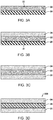
- Figs. 3A to 3D are diagrams schematically illustrating cross sections in the steps of Production Example A. Production Example A will be described with reference to Figs. 3A to 3D .
- a B-stage resin layer 22 is formed by applying a resin layer composition on a release layer 20, and a "B-stage resin layer/release layer laminate" (also referred to as a "B-stage sheet") is produced.
- a release layer 20 a known film such as a PET film may be used.
- the PET film is not particularly limited, and may be, for example, Panaprotect MK38S available from PANAC Co., Ltd.
- the method for applying the resin layer composition may be a known application method. For example, it is preferable to apply the composition while adjusting the film thickness using a bar coater.
- the semi-cured B-stage resin layer 22 is formed using a known heating means such as an oven after the resin layer composition is applied to the release layer 20 as described above.
- the heating temperature is preferably from 50 to 150°C, and more preferably from 70 to 130°C.
- the heating may be performed in two stages, such as from 50 to 100°C and from 100 to 150°C.
- the total heating time is preferably less than 30 minutes, and more preferably less than 20 minutes.
- the surface roughness Ra of the B-stage resin layer 22 exposed on the surface is preferably from 1 to 100 nm, and more preferably from 10 to 50 nm.
- the surface roughness Ra of the B-stage resin layer 22 is within the above range, the adhesion between the resin layer and the metal layer or between the resin layers can be further improved when producing a high-frequency circuit laminate.
- the surface roughness Ra of the B-stage resin layer in the present invention refers to "arithmetic mean roughness" measured according to JIS B0601-2001.
- the elastic modulus of the B-stage resin layer 22 is preferably such that the maximum value of the elastic modulus (MPa) is 1 MPa or greater, and more preferably 3 MPa or greater at 50°C or higher and lower than 80°C under the measurement condition of 1 Hz.
- the minimum value of the elastic modulus (MPa) in the temperature range of 80°C or higher and 200°C or lower is preferably 20 MPa or less, and more preferably 15 MPa or less.
- the exposed resin layer surface 23 of the "B-stage resin layer/release layer laminate" produced in the step A1 is bonded to the metal layer 24 to produce a "metal layer/B-stage resin layer/release layer laminate".
- the surface roughness Ra of the metal layer 24 bonded to the resin layer surface 23 is preferably from 10 to 300 nm, more preferably from 30 to 200 nm, and particularly preferably from 30 to 100 nm.
- the resin layer surface 23 of the "B-stage resin layer/release layer laminate" and the metal layer 24 are overlaid, and then preferably thermocompressed using a heated roll (also referred to as a "hot roll” in the present specification) or the like.
- the linear load at the time of thermocompression bonding is preferably from 1 to 19 kN/m, and more preferably from 5 to 18 kN/m.
- the temperature of the thermocompression bonding is preferably from 50 to 200°C, more preferably from 50 to 150°C, and particularly preferably from 70 to 130°C.
- the "metal layer/B-stage resin layer/release layer laminate" immediately after bonding may be further subjected to annealing treatment by subsequently contacting the laminate with a heated roll or passing it through a heating furnace.
- the annealing treatment may be performed at a temperature equal to or higher than the melting point of the resin, and is preferably, for example, from 100 to 250°C, and more preferably from 110 to 230°C.
- the heating time is not particularly limited, but is preferably from 5 to 600 seconds, and more preferably from 10 to 300 seconds.
- the release layer can be peeled off satisfactorily in the production process.
- the above-described "the "metal layer/B-stage resin layer/release layer laminate” immediately after bonding" is further treated” refers to the step in which the laminate, which had been bonded in the production line for bonding the laminate, is further treated in-line after the bonding treatment, without taking out the bonded laminate from the production line.
- the release layer 20 is peeled off from the "metal layer/B-stage resin layer/release layer laminate" produced in the step A2, and the exposed resin layer surface 21 and the metal foil 26 are bonded as necessary.
- the release layer 20 is peeled off from the "metal layer/B-stage resin layer/release layer laminate” and the exposed B-stage resin layer surface 21 is bonded to the metal layer 26, it is preferable that the exposed resin layer surface 21 and the metal layer 26 are overlaid, and further subjected to thermocompression bonding using a hot roll or the like.
- the thermocompression bonding is preferably performed under the same conditions as in the step A2.
- the surface roughness Ra of the resin layer surface 21 exposed by peeling the release layer 20 from the "metal layer/B-stage resin layer/release layer laminate" is preferably from 1 to 100 nm, and more preferably from 10 to 50 nm.
- the surface roughness Ra of the B-stage resin layer is within the above range, when producing a high-frequency circuit laminate, the adhesion between the resin layer and the metal layer or between the resin layers can be further improved.
- the B-stage resin layer 22 is cured to form a C-stage resin layer 28, thereby obtaining a high-frequency circuit laminate 200.
- the laminate obtained in the step A3 is preferably heated to 50 to 200°C, and more preferably to 100 to 200°C using a known heating means such as an oven.
- the heating may be performed in two stages such as from 50 to 100°C and from 100 to 200°C.
- the heating time is preferably less than 5 hours, and more preferably less than 3 hours.
- Figs. 4A to 4C are diagrams schematically illustrating the cross sections in the steps of Production Example B. Production Example B will be described with reference to Figs. 4A to 4C .
- a resin layer composition is applied to the metal layer 30 to form a B-stage resin layer 32, thereby producing a "metal layer/B-stage resin layer laminate".
- the coating method of the resin layer composition may be a known coating method, but it is preferable to use a bar coater to adjust the film thickness of the coating.
- the semi-cured B-stage resin layer 32 After the resin layer composition is applied to the metal layer 30 as described above, it is preferable to form the semi-cured B-stage resin layer 32 using a known heating means such as an oven.
- the heating temperature is preferably from 50 to 150°C, and more preferably from 70 to 130°C.
- the heating may be performed in two stages, such as from 50 to 100°C and from 100 to 150°C.
- the total heating time is preferably less than 30 minutes, and more preferably less than 20 minutes.
- the metal layer 34 is bonded to the exposed resin layer surface 33 of the "metal layer/B-stage resin layer laminate" produced in the step B1, thereby producing a "metal layer/B-stage resin layer/metal layer laminate".
- the exposed resin layer surface 33 and the metal layer 34 are overlaid, and then thermocompressed using a hot roll or the like.
- the thermocompression bonding is preferably performed under the same conditions as in the step A2.
- an annealing process may be performed by continuing the "metal layer/B-stage resin layer/metal layer" immediately after the bonding by contacting the heated roller or passing it through the heating furnace.
- the annealing treatment is preferably performed under the same conditions as in the step A2.
- the surface roughness Ra of the exposed resin layer surface 33 is preferably from 1 to 100 nm, and more preferably from 10 to 50 nm.
- the surface roughness Ra of the B-stage resin layer is within the above-described range, the adhesion between the resin layer and the metal layer can be further improved when producing a high-frequency circuit laminate.
- the surface roughness Ra of the metal layer 34 to be bonded to the resin layer surface 33 is preferably from 10 to 300 nm, more preferably from 30 to 200 nm, and particularly preferably from 30 to 100 nm.
- the B-stage resin layer 32 is cured to form a C-stage resin layer 36, thereby obtaining a high-frequency circuit laminate 300.
- the "metal layer/B-stage resin layer/metal layer laminate" produced in the step B2 is preferably heated to 50 to 200°C, and more preferably heated to 100 to 200°C using a known heating means such as an oven.
- the heating may be performed in two stages, such as from 50 to 100°C and from 100 to 200°C.
- the heating time is preferably less than 5 hours, and more preferably less than 3 hours.
- a circuit board such as FPC can be produced using the high-frequency circuit laminate thus obtained.
- the transmission loss can be reduced even when driven at a high frequency by using the above-described high-frequency circuit laminate as at least a part of the laminate structure.
- Such a circuit board is required to include the above-described high-frequency circuit laminate as a part of a laminated structure, and can be produced by applying the production process described in, for example, WO 2012/014339 and JP 2009-231770 A .
- a circuit board can be produced by, for example, laminating the above-described high-frequency circuit laminate, patterning the metal layer of the above-described high-frequency circuit laminate by etching, drilling it, or cutting it to a required size.
- Such a circuit board can be produced by, for example,
- the method for laminating the resin film on the circuit board in the step (a) is not particularly limited, and examples thereof include lamination methods using a multi-stage press, a vacuum press, a normal pressure laminator, or a laminator that heats and presses under vacuum. Among them, the method using a laminator that heats and presses under vacuum is preferable. As a result, even if the circuit board has a fine wiring circuit on the surface, there is no void and the space between the circuits can be embedded with the resin.
- the lamination conditions are not particularly limited, but the compression temperature is from 70 to 130°C, the compression pressure is from 1 to 11 kgf/cm 2 , and the lamination is preferably performed under reduced pressure or vacuum.
- the lamination may be performed by a batch system or a continuous system using rolls.
- the circuit substrate is not particularly limited, and may be, for example, a glass epoxy substrate, a metal substrate, a polyester substrate, a polyimide substrate, a BT resin substrate, a thermosetting polyphenylene ether substrate, or a fluororesin substrate.
- the circuit surface of the surface on which the resin film of the circuit board is laminated may be pre-roughened.
- the number of circuit layers of the circuit board is not limited. For example, when producing a printed wiring board for a millimeter-wave radar, the number of circuit layers may be freely selected from 2 to 20 according to the design.
- the resin film and the circuit board laminated in the step (a) are heated and pressed to flatten.
- the conditions are not particularly limited, but the temperature is preferably from 100°C to 250°C, the pressure is preferably from 0.2 to 10 MPa, and the time is preferably from 30 to 120 minutes, and the temperature is more preferably from 150°C to 220°C.
- a circuit layer is further formed on the resin layer formed by heating and pressing the resin film and the circuit board.
- the method for forming the circuit layer formed on the resin layer as described above is not particularly limited.
- the circuit layer may be formed by, for example, an etching method such as a subtractive method, or a semi-additive method.
- the subtractive method is a method for forming a desired circuit, including forming an etching resist layer having a shape corresponding to a desired pattern shape on a metal layer, and dissolving and removing the metal layer in a portion, where the resist has been removed, with a chemical solution by a subsequent development process.
- the semi-additive method is a method for forming a desired circuit layer, including forming a metal film on the surface of the resin layer by electroless plating, forming a plating resist layer having a shape corresponding to a desired pattern on the metal film, and then forming a metal layer by electrolytic plating, followed by removing unnecessary electroless plating layer with a chemical solution or the like.
- holes such as via holes may be formed in the resin layer as needed.
- the method for forming the holes is not limited, and may use, for example, an NC drill, a carbon dioxide laser, a UV laser, a YAG laser, or plasma.
- the glass transition temperature (Tg) was measured using a dynamic viscoelasticity measuring device ("DMS7100" available from Seiko Instruments Inc.) at a frequency of 1 Hz and a temperature rising rate of 10°C/minute, and used the temperature at which the loss tangent was at a maximum.
- the loss tangent was a value obtained by dividing the storage elastic modulus by the loss elastic modulus.
- the weight average molecular weight (Mw) was measured under the following conditions using a GPC apparatus ("HLC-8320" available from Tosoh Corporation).
- HPC-8320 available from Tosoh Corporation
- Detector differential refractometer Standard substance: monodisperse polystyrene
- the resin layer composition prepared above was coated on a 100 ⁇ m thick PET film (Teijin Tetron Film G2 available from Teijin Film Solutions Co., Ltd.) with a bar coater so that the film thickness after curing was 25 ⁇ m, and heated at 70°C for 10 minutes using an oven. Thereafter, the coating was heated at 130°C for 10 minutes, thereby obtaining a "B-stage resin layer/release layer laminate" in which the B-stage resin layer was laminated on the PET film.
- PET film Teijin Tetron Film G2 available from Teijin Film Solutions Co., Ltd.
- the surface of the resin layer of the "B-stage resin layer/release layer laminate” obtained above was measured using a white interference microscope (New View 5032 available from ZYGO Corporation), and "arithmetic average roughness" calculated for the 10 ⁇ m ⁇ 10 ⁇ m range in accordance with JIS B0601-2001 was used as the surface roughness Ra.
- the results are shown in Table 1.
- the release layer (PET film) was peeled off from the "B-stage resin layer/release layer laminate" obtained above, a test piece (width 3 mm ⁇ length 2 cm) was cut out, and the maximum value of the elastic modulus (MPa) in the temperature range of 50°C or higher and lower than 80°C and the minimum value of the elastic modulus (MPa) in the temperature range of 80°C or higher and 200°C or lower was measured using a DMS tester (available from Seiko Instruments Inc.) under the measurement condition of 1 Hz and 10°C/min. The results are shown in Table 1.
- a 18 ⁇ m thick copper foil (model number "TQ-M4-VSP", surface roughness 110 nm, available from Mitsui Mining & Smelting Co., Ltd.) was overlaid on the exposed resin layer of the "B-stage resin layer/release layer laminate" obtained above, further the laminate was pressed with a hot roll at 150°C under a linear load of 10 kN/m, thereby producing a "metal layer/B-stage resin layer/release layer laminate" having a laminate structure of copper foil/B-stage resin layer/PET film.
- the surface roughness Ra of the copper foil was measured using a white interference microscope (New View 5032 available from ZYGO), and the "arithmetic mean roughness" calculated for the 10 ⁇ m ⁇ 10 ⁇ m range was defined as the surface roughness Ra in accordance with JIS B0601-2001. The results are shown in Table 1.
- the release layer (PET film) was peeled off from the "metal layer/B-stage resin layer/release layer laminate" obtained above, and the surface of the exposed resin layer was measured using a white interference microscope (New View 5032 available from ZYGO Corporation), and the "arithmetic mean roughness" calculated for a range of 10 ⁇ m ⁇ 10 ⁇ m in accordance with JIS B0601-2001 was used as the surface roughness Ra.
- the results are shown in Table 1.
- the release layer (PET film) was peeled off from the "metal layer/B-stage resin layer/release layer laminate" obtained above, and the exposed resin layer surface and an 18 ⁇ m thick copper foil (model number "TQ-M4-VSP", surface roughness 110 nm, available from Mitsui Mining & Smelting Co., Ltd.) were placed on top of each other, pressed with a hot roll at 150°C under a linear load of 10 kN/m, and then heated at 250°C for 3 hours using an oven, thereby producing a high-frequency circuit laminate having a laminated structure of "copper foil (film thickness: 18 ⁇ m)/C-stage resin layer (film thickness: 25 ⁇ m)/copper foil (film thickness: 18 ⁇ m)" in which copper foil was laminated on both sides of the C-stage resin layer.
- the surface roughness Ra of the copper foil (metal layer) was measured using a white interference microscope (New View 5032, available from ZYGO Corporation), and the "arithmetic average roughness" calculated for a range of 10 ⁇ m ⁇ 10 ⁇ m based on JIS B0601-2001 was defined as the surface roughness Ra.
- Table 1 The results are shown in Table 1.
- the produced high-frequency circuit laminate was subjected to etching treatment to remove the copper foil, thereby producing a resin film for evaluation.
- a dumbbell-shaped test piece of JIS K 7161 7 was cut out from the prepared resin film, and pulled at 5 mm/min using "Ez-LX" available from Shimadzu Corporation, and the stress and elongation at break were measured as tensile strength and tensile elongation, respectively. The results are shown in Table 1.
- the produced high-frequency circuit laminate was subjected to etching treatment to remove the copper foil, thereby producing a resin film for evaluation.
- a test piece (width 3 mm ⁇ length 1 cm) was cut out from the prepared resin film, and the glass transition temperature (Tg) was measured using a DMS tester (model number "EXSTAR4000", available from Seiko Instruments Inc.). The results are shown in Table 1.
- the produced high-frequency circuit laminate was subjected to etching treatment to remove the copper foil, thereby producing a resin film for evaluation.
- a dumbbell-shaped test piece of JIS K7161 7 was cut out from the prepared resin film, and a tensile test was performed at 5 mm/min in accordance with JIS K7161 using "Ez-LX" available from Shimadzu Corporation to measure the tensile modulus of elasticity. The results are shown in Table 1.
- the produced high-frequency circuit laminate was subjected to etching treatment to remove the copper foil, thereby producing a resin film for evaluation.
- a test piece (2.6 mm wide ⁇ 80 mm long) was cut out from the produced resin film and measured for the relative permittivity and the dielectric loss tangent at 10 GHz using a dielectric constant measuring device by cavity perturbation method (model No. "PNA-L Network Analyzer N5230A” available from Agilent Technologies and a model number "Cavity Resonator CP 531 for 10 GHz” available from Kanto Electronic Application and Development Inc.). The results are shown in Table 1.
- test piece (1 cm wide ⁇ 10 cm long) was cut out from the produced high-frequency circuit laminate, and was pulled in the direction of 90° at 500 mm/min using "Instron 5567" available from Instron, and the peel strength was measured in accordance with "IPC-TM-650 2.4.9". The results are shown in Table 1.
- One side of the high-frequency circuit laminate prepared above was patterned with a copper foil using a photosensitive dry film, and copper wiring patterns having a pitch of 150 ⁇ m and a line width of 40, 45, 50, 55 and 60 ⁇ m, and a pitch of 750 ⁇ m and a line width of 200, 220, 240, 260 and 280 ⁇ m were prepared.
- the "B-stage resin layer/release layer laminate" prepared as described above was placed in such a manner that the B-stage resin layer side contacts the copper wiring of the patterned high-frequency circuit laminate, and then a panel board was placed thereon. After forming with heat and pressure under pressing conditions at 120°C/3.0 MPa/5 min, the release layer (PET film) was peeled off, followed by heating at 250°C for 3 hours to produce a circuit board.
- the circuit board prepared above was measured for the transmission loss at a frequency of 20 GHz at 25°C using a measurement probe (Single (ACP40GSG250), available from Cascade Microtech, Inc.) and a vector network analyzer (E8363B, available from Keysight technology). When the transmission loss was -5 dB/100mm or greater, it was judged to be good.
- Both surfaces of the high-frequency circuit laminate prepared above were etched so that the thickness of the copper foil was 9 ⁇ m, further the copper foil was patterned using a photosensitive dry film to prepare a copper wiring pattern having a pitch of 100 ⁇ m and a line width of 50 ⁇ m.
- the release layer (PET film) was peeled off from the "metal layer/B-stage resin layer/release layer laminate" produced above, the laminate was arranged on both sides so that the peeled and exposed resin layer and the prepared copper wiring pattern were in contact with each other. Further, the object was sandwiched between end plates, heated and pressed under pressing conditions of 120°C/1.1 MPa/2 minutes, and further heated at 250°C for 3 hours.
- the copper foil was patterned using a photosensitive dry film, and a copper wiring pattern with a pitch of 100 ⁇ m and a line width of 50 ⁇ m was formed on both sides.
- the release layer (PET film) was peeled off from the "B-stage resin layer/release layer laminate" produced above, the laminate was arranged on both sides so that the resin layer on the release surface and the prepared copper wiring pattern are in contact with each other. Further, the object was sandwiched between end plates, formed by heating and pressing under pressing conditions of 120°C/1.1 MPa/2 minutes, followed by further heating at 250°C for 3 hours, thereby producing an evaluation substrate having four layers of copper wiring.
- the cross-sectional shape of the produced substrate for evaluation was observed using a scanning electron microscope.
- the difference between the recessed part and the convex part was 5% or less, the substrate was judged to be practical and good, and when the difference was greater than 5%, the substrate was judged to be impractical and defective.
- the results are shown in Table 1.
- a circuit board was produced and evaluated in the same manner as in Example 1 except that the resin layer composition was changed to the composition shown in Table 1, and the type of the metal film and various thickness and the lamination conditions were changed as shown in Table 1. The results are shown in Table 1.
- the resin layer composition prepared in Example 1 was coated on a 18 ⁇ m thick copper foil (model number "TQ-M4-VSP", surface roughness 110 nm, available from Mitsui Mining & Smelting Co., Ltd.) with a bar coater so that the film thickness after curing was 25 ⁇ m, and heated at 70°C for 10 minutes using an oven. Thereafter, the coating was heated at 130°C for 10 minutes to produce a "metal layer/B-stage resin layer laminate" having a laminate structure of copper foil/B-stage resin layer.
- the resin layer composition was prepared in the same manner as in Example 1 so as to have the composition shown in Table 1, coated on a 18 ⁇ m thick copper foil (model number "TQ-M4-VSP", surface roughness 110 nm, available from Mitsui Mining & Smelting Co., Ltd.) with a bar coater so that the film thickness after curing was 25 ⁇ m, and heated at 70°C for 10 minutes using an oven. Thereafter, the coating was heated at 130°C for 10 minutes, and further heated at 250°C for 3 hours.
- Table 1 shows the resin layer composition used in each of the examples and comparative examples, and the evaluation results of the high-frequency circuit laminates and the circuit boards.
Landscapes
- Engineering & Computer Science (AREA)
- Microelectronics & Electronic Packaging (AREA)
- Manufacturing & Machinery (AREA)
- Chemical & Material Sciences (AREA)
- Medicinal Chemistry (AREA)
- Chemical Kinetics & Catalysis (AREA)
- Health & Medical Sciences (AREA)
- Polymers & Plastics (AREA)
- Organic Chemistry (AREA)
- Laminated Bodies (AREA)
- Chemical And Physical Treatments For Wood And The Like (AREA)
- Polysaccharides And Polysaccharide Derivatives (AREA)
- Manufacturing Of Printed Wiring (AREA)
- Non-Metallic Protective Coatings For Printed Circuits (AREA)
- Production Of Multi-Layered Print Wiring Board (AREA)
Abstract
(A - B)/B ≤ 0.1
wherein A is the maximum value of the thickness in the wiring portion (µm) and B is the minimum value of the thickness in the non-wiring portion (µm).
Description
- The present invention relates to a circuit board including a wiring portion having a resin layer and a metal layer.
- With the recent increase in the performance of information terminal equipment and dramatic advances in network technology, the frequency of electric signals handled in the information communication field has been increasing toward high speed and large capacity transmission. In order to address this, there is an increasing demand for low dielectric constant (low εr) and low dielectric loss tangent (low tan δ) materials that can reduce the transmission loss, which is a problem when transmitting and processing high-frequency signals and high-speed digital signals to the printed wiring boards used (for example, see Patent Documents 1 to 4).
- As printed wiring boards, a flexible printed circuit board (hereinafter also referred to as "FPC") and a flexible flat cable (hereinafter also referred to as "FFC") are used for electronic and electric devices. The FPC is produced by the steps of processing a copper clad laminate (CCL) including an insulator layer and a copper foil layer to form an electrical circuit, and then attaching an adhesive portion of a coverlay (CL) including an insulating layer and an adhesive layer to the circuit portion to protect the circuit portion. Additionally, FFC is an electrical circuit obtained by using a substrate made of an insulator layer and an adhesive layer and a conductor such as copper foil formed in a wiring form, arranging a plurality of conductors between the adhesive parts of the substrate, and bonding.
-
- Patent Document 1:
JP 2014-197611 A - Patent Document 2:
JP 2015-176921 A - Patent Document 3:
JP 2016-087799 A - Patent Document 4:
JP 2016-032098 A - However, electrical signals tend to be attenuated at higher frequencies, and the transmission loss tends to increase. Therefore, mounting boards for next-generation high-frequency (10 GHz or higher), low dielectric for reducing crosstalk between wires and low dielectric loss characteristics for suppressing the transmission loss of electrical signals have become indispensable characteristics for insulator materials. Furthermore, in order to suppress the transmission loss of electrical signals, it is also important that the mounting substrate has excellent smoothness. In particular, in FPC and FFC, an adhesive is used to laminate the resin layer and the metal layer, but the adhesive layer formed by the adhesive is considered to be one of the causes of impairing the low dielectric loss characteristics and the smoothness of the mounting substrate.
- The present invention has been made in view of the above circumstances, and an object of the present invention is to provide a circuit board having excellent smoothness and capable of reducing a transmission loss of a high-frequency signal.
- The present invention has been made to achieve at least part of the above object, and can be achieved as the following embodiments or the application examples.
- An embodiment of the circuit board according to the present invention includes a wiring portion and a non-wiring portion,
the wiring portion having a metal layer and a resin layer,
the non-wiring portion having a resin layer,
the resin layer at a frequency 10GHz having a relative permittivity of from 2 to 3 at 23°C, and
the circuit board satisfying a relationship:
(A - B)/B ≤ 0.1
in which A is a maximum value of a thickness in the wiring portion (µm) and B is a minimum value of a thickness in the non-wiring portion (µm). - The circuit board according to Application Example 1, in which the metal layer and the resin layer in the wiring portion may be laminated in contact with each other.
- The circuit board according to Application Example 1 or 2, in which a dielectric loss tangent of the resin layer may be from 0.001 to 0.01 at a frequency of 10 GHz at 23°C.
- The circuit board according to any one of Application Examples 1 to 3, in which an elastic modulus of the resin layer may be from 0.1 to 3 GPa.
- The circuit board according to any one of Application Examples 1 to 4, in which a peel strength between the resin layer and the metal layer may be 5 N/cm or greater.
- The circuit board according to any one of Application Examples 1 to 5, in which a thickness of the resin layer may be from 10 to 100 µm, and a thickness of the metal layer may be from 10 to 50 µm.
- The circuit board of the present invention has excellent smoothness and is capable of reducing a transmission loss of a high-frequency signal.
-
-
Fig. 1 is a cross-sectional view schematically illustrating a circuit board according to the present embodiment -
Fig. 2 is a plan view cut along the line C-C 'inFig. 1 . -
Fig. 3A is a cross-sectional view schematically illustrating the step A1 in Production Example A of the high-frequency circuit laminate. -
Fig. 3B is a cross-sectional view schematically illustrating a step A2 in Production Example A of the high-frequency circuit laminate. -
Fig. 3C is a cross-sectional view schematically illustrating a step A3 in Production Example A of the high-frequency circuit laminate. -
Fig. 3D is a cross-sectional view schematically illustrating a step A4 in Production Example A of the high-frequency circuit laminate. -
Fig. 4A is a cross-sectional view schematically illustrating a step B1 in Production Example B of the high-frequency circuit laminate. -
Fig. 4B is a cross-sectional view schematically illustrating a step B2 in Production Example B of the high-frequency circuit laminate. -
Fig. 4C is a cross-sectional view schematically illustrating a step B3 in Production Example B of the high-frequency circuit laminate. - Preferred embodiments according to the present invention will be described below in detail. It should be understood that the present invention is not limited to only the embodiments described below, but also includes various modifications that are made without departing from the spirit of the present invention.
- In this specification, a numerical range described with "from A to B" is meant to include a numerical value A as a lower limit value and a numerical value B as an upper limit value.
- The terms used in the present specification are defined as follows.
- The "high-frequency signal" refers to an electric signal or a radio wave having a frequency of 10 GHz or higher.
- The "high-frequency circuit laminate" refers to a laminated body used when producing a high-frequency circuit driven at a frequency of 10 GHz or higher.
- The "B-stage resin layer" refers to a layer in which the resin is semi-cured.
- The "C-stage resin layer" refers to a layer in which the resin is completely cured. Note that in the present invention, the "C-stage resin layer" may be simply referred to as a "resin layer".
- In addition, the direction herein is defined as follows. That is, three spatial axes orthogonal to each other are defined as an X axis, a Y axis, and a Z axis. The vertical direction is the direction along the Z-axis direction (Z direction), the vertical downward direction is the -Z direction, and the vertical upward direction is the +Z direction. The plane perpendicular to the Z axis is taken as an XY plane.
- The circuit board according to the present embodiment includes a wiring portion and a non-wiring portion, the wiring portion having a metal layer and a resin layer, the non-wiring portion having a resin layer,
the resin layer at a frequency 10GHz having a relative permittivity of from 2 to 3 at 23°C, and the circuit board satisfying a relationship:
(A - B)/B ≤ 0.1
in which A is the maximum value of the thickness in the wiring portion (µm) and B is the minimum value of the thickness in the non-wiring portion (µm). Below, the circuit board according to the present embodiment will be described in detail with reference to the drawings. -
Fig. 1 is a cross-sectional view schematically illustrating a circuit board according to the present embodiment.Fig. 2 is plan view cut along the line C-C' ofFig. 1 . As illustrated inFig. 1 , acircuit board 100 includes aresin layer 12 and ametal layer 14 on a substrate 10 (in the +Z direction). In the example ofFig. 1 , theresin layer 12 is laminated on the metal layer 14 (in the +Z direction), so that theresin layer 14 existing above themetal layer 14 is in a state of being raised in the +Z direction more than theother resin layer 14. - The
substrate 10 is not particularly limited, and may be, for example, a glass epoxy substrate, a metal substrate, a polyester substrate, a polyimide substrate, a BT resin substrate, a thermosetting polyphenylene ether substrate, or a fluororesin substrate. Alternatively, the high-frequency circuit laminate described below may be used as a substrate when producing a multilayer circuit board. - In the circuit board according to the present embodiment, the portions of the
metal layer 14 and the resin layer 12 (that is, a region 16) laminated on the metal layer 14 (in the +Z direction) as shown inFig. 1 are defined as a "wiring portion", and the portion of theresin layer 12 other than the wiring portion is defined as "non-wiring portion". - The circuit board according to the present embodiment satisfies the relationship (A - B)/B ≤ 0.1, in which A is the maximum value of the thickness at the wiring portion (µm) and B is the minimum value of the thickness at the non-wiring portion (µm). The (A - B) is ΔH in
Fig. 1 . The (A - B)/B is preferably 0.09 or less, and more preferably 0.08 or less, and even more preferably 0.07 or less, yet even more preferably 0.06 or less, and particularly preferably 0.05 or less. In such a circuit board, theresin layer 12 laminated on the metal layer 14 (in the +Z direction), which is a projection of the wiring portion, does not form a large step, and the entire surface of theresin layer 14 is in a smooth state. For this reason, even if circuit boards are laminated, high positioning accuracy can be satisfied, and more layers of circuits can be integrated. - In the present invention, even when such a circuit board is laminated to produce a multilayer circuit board, the maximum value A (µm) of the thickness in the wiring portion and the minimum value B (µm) of the thickness in the non-wiring portion are defined for each resin layer.
- In the circuit board according to the present embodiment, the
metal layer 14 and theresin layer 12 are preferably laminated in contact with each other. That is, it is preferable that no adhesive layer such as a primer resin layer is interposed between the metal layer and the resin layer. In a general circuit board, an adhesive layer is interposed between the resin layer and the metal layer in order to improve the adhesion between the metal layer having the conductive function and the resin layer having the insulating function. The adhesive layer is formed by a method such as application using an adhesive mainly containing a polymer having a polar functional group. However, such an adhesive layer has poor electrical characteristics, so that the effective dielectric constant and effective dielectric loss of the resin layer having an insulating function are increased, and are not suitable for high-frequency circuits. In contrast, the circuit board according to the present embodiment has good adhesion between the metal layer and the resin layer without using an adhesive, and the metal layer and the resin layer are laminated in contact with each other. As a result, a circuit board suitable for a high-frequency circuit was successfully obtained without deteriorating the effective electrical characteristics of the resin layer. - In the circuit board according to the present embodiment, the peel strength between the resin layer and the metal layer is preferably 5 N/cm or greater, more preferably 5.3 N/cm or greater, and particularly preferably 6 N/cm or greater. Since the circuit board according to the present embodiment has a peel strength in the above-described range, the adhesion between the metal layer and the resin layer is good even without using an adhesive. Note that the peel strength can be measured in accordance with the method described in "IPC-TM-650 2.4.9".
- Hereinafter, the configuration and production method of each layer constituting the circuit board according to the present embodiment will be described in detail.
- The circuit board according to the present embodiment includes a resin layer. The elastic modulus of the resin layer is preferably from 0.1 to 3 GPa, and more preferably from 0.2 to 2.5 GPa. When the elastic modulus of the resin layer is within the above range, a circuit board having excellent flexibility can be obtained, so that a circuit board can be produced under more free conditions. The elastic modulus of the resin layer is a tensile modulus of elasticity, and can be measured in accordance with JIS K7161.
- The relative permittivity of the resin layer at a frequency of 10 GHz at 23°C is from 2 to 3, and preferably from 2.1 to 2.8. When the relative permittivity at 10 GHz is within the above range, a circuit board having excellent high-frequency characteristics can be produced. In addition, the dielectric loss tangent of the resin layer at a frequency of 10 GHz at 23°C is preferably from 0.001 to 0.01, and more preferably from 0.002 to 0.009. When the dielectric loss tangent at a frequency of 10 GHz is within the above range, a circuit board having excellent high-frequency characteristics can be produced. The relative permittivity and the dielectric loss tangent at a frequency of 10 GHz can be measured using a cavity resonator perturbation method dielectric constant measurement device.
- In addition, the thickness of the resin layer is preferably from 10 to 100 µm, more preferably from 20 to 90 µm, and particularly preferably from 25 to 80 µm.
- The present invention also includes an embodiment in which the resin layer is composed of a plurality of different resin layers. When the resin layer includes a plurality of resin layers, the elastic modulus, relative permittivity, and dielectric loss tangent of each resin layer need not necessarily be limited to the preferable ranges described above, and is required to be in a preferred range as a whole.
- The method for producing the resin layer is not particularly limited, and it can be produced by a method such as applying the resin layer composition to a substrate such as a release layer or a metal foil, or extruding the composition to produce a self-standing film.
- The composition of the resin layer composition is not particularly limited as long as the resin layer to be obtained has a composition satisfying the relative permittivity described above, and preferably contains a polymer, a curable compound, and as necessary, a curing aid and a solvent.
- As the polymer that can be included in the resin layer composition, for example, a known material having low dielectric constant and low dielectric loss tangent characteristics such as an epoxy resin, a polyimide, or a polyarylene may be used as appropriate. In particular, a polymer having a repeating unit represented by at least one of Formulas (1-1), (1-2) and (1-3) below are preferably used.

- (Where in Formulas (1-1) to (1-3), R1 are each independently a halogen atom, a monovalent hydrocarbon group having from 1 to 20 carbon atoms, a monovalent halogenated hydrocarbon group having from 1 to 20 carbons, a nitro group, a cyano group, any of primary to tertiary amino groups, or any of salts of primary to tertiary amino groups. The n is each independently an integer from 0 to 2. In a case where n is 2, the plurality of R1s may be the same or different, and may be bonded in any combination to form part of a ring structure.)
- The R1 is preferably a halogen atom, a monovalent hydrocarbon group having from 1 to 6 carbon atoms, a monovalent halogenated hydrocarbon group having from 1 to 6 carbon atoms, a nitro group, a cyano group, a primary to tertiary amino group, or a salt of a primary to tertiary amino group, and more preferably a fluorine atom, a chlorine atom, a methyl group, a nitro group, a cyano group, a t-butyl group, a phenyl group, or an amino group. The n is preferably 0 or 1, and more preferably 0.
- The position of the other bond with respect to one bond of the repeating unit is not particularly limited, but the meta position is preferred from the viewpoint of improving the polymerization reactivity of the monomer giving the repeating unit. The repeating unit is preferably a structural unit having a pyrimidine skeleton and represented by Formula (1-2) above.
- The polymer may have a repeating unit other than the repeating unit represented by at least one of Formulas (1-1), (1-2) and (1-3) above as necessary, and the content ratio of the repeating unit represented by at least one of Formulas (1-1), (1-2) and (1-3) above in the polymer is preferably from 5 to 95 mol%, and more preferably from 10 to 60 mol% when the total of all the structural units in the polymer is 100 mol%.
- The method for synthesizing the polymer having a repeating unit represented by at least one of Formulas (1-1), (1-2) and (1-3) above is not particularly limited, and may be a known method. For example, it can be synthesized by heating a monomer that provides a repeating unit represented by at least one of Formulas (1-1), (1-2) and (1-3) above and other monomer as necessary in an organic solvent together with an alkali metal or the like.
- The lower limit of the weight average molecular weight (Mw) of the polymer having a repeating unit represented by at least one of Formulas (1-1), (1-2) and (1-3) above is preferably 500, more preferably 1000, still more preferably 10000, and particularly preferably 30000. The upper limit of the weight average molecular weight (Mw) is preferably 600000, more preferably 400000, even more preferably 300000, and particularly preferably 200000.
- The lower limit of the glass transition temperature (Tg) of the polymer having a repeating unit represented by at least one of Formulas (1-1), (1-2) and (1-3) above is preferably 150°C, and more preferably 180°C. The upper limit of the glass transition temperature (Tg) is preferably 320°C, and more preferably 300°C.
- The polymer preferably further has a repeating unit represented by General Formula (2) below.


- (In Formula (2), R3 and R4 are each independently a halogen atom, a nitro group, a cyano group, or a divalent organic group having from 1 to 20 carbon atoms, c and d are each independently an integer from 0 to 8, e, f, and y are each independently an integer of 0 to 2, and L is a single bond, -O-, -S-, -CO-, -SO-, -SO2-, or a divalent organic group having from 1 to 20 carbon atoms.)
- Examples of the halogen atoms represented by R3 and R4 include a fluorine atom, a chlorine atom, a bromine atom and an iodine atom.
- Examples of the monovalent hydrocarbon group having from 1 to 20 carbons represented by R3 and R4 include a monovalent linear hydrocarbon group, a monovalent alicyclic hydrocarbon group, and a monovalent aromatic hydrocarbon group.
- Examples of the monovalent linear hydrocarbon group include alkyl groups such as a methyl group, an ethyl group, a n-propyl group, an i-propyl group, a n-butyl group, an i-butyl group, a sec-butyl group, a t-butyl group, a n-pentyl group; alkenyl groups such as an ethenyl group, a propenyl group, a butenyl group, and a pentenyl group; and alkynyl groups such as an ethynyl group, a propynyl group, a butynyl group, and a pentynyl group.
- Examples of the monovalent alicyclic hydrocarbon group include monocyclic cycloalkyl groups such as a cyclopropyl group, a cyclobutyl group, a cyclopentyl group, and a cyclohexyl group; polycyclic cycloalkyl groups such as a norbornyl group and an adamantyl group; monocyclic cycloalkenyl groups such as a cyclopropenyl group, a cyclobutenyl group, a cyclopentenyl group, and a cyclohexenyl group; and polycyclic cycloalkenyl groups such as a norbornenyl group.
- Examples of the monovalent aromatic hydrocarbon group include aryl groups such as a phenyl group, a tolyl group, a xylyl group, a naphthyl group, and an anthryl group; and aralkyl groups such as a benzyl group, a phenethyl group, a phenylpropyl group, and a naphthylmethyl group.
- Examples of the monovalent halogenated hydrocarbon group having 1 to 20 carbon atoms represented by R3 and R4 include groups in which part or all of the hydrogen atoms of the monovalent hydrocarbon group having from 1 to 20 carbon atoms exemplified as the group represented by R3 and R4 is substituted with a halogen atom such as a fluorine atom, a chlorine atom, a bromine atom, or an iodine atom.
- Examples of the divalent organic group having from 1 to 20 carbon atoms represented by L include divalent linear hydrocarbon groups having from 1 to 20 carbon atoms, divalent fluorinated linear hydrocarbon groups having from 1 to 20 carbon atoms, divalent aromatic hydrocarbon groups having from 6 to 20 carbon atoms, and divalent fluorinated aromatic hydrocarbon groups having from 6 to 20 carbon atoms.
- Examples of the divalent linear hydrocarbon group include a methylene group, an ethylene group, an n-propylene group, an isopropylene group, an n-butylene group, a sec-butylene group, a t-butylene group, a neopentylene group, a 4-methyl-pentane-2,2-diyl group, and a nonane-1,9-diyl group
- Examples of the divalent alicyclic hydrocarbon group include monocyclic cycloalkyl groups such as a cyclopropyl group, a cyclobutyl group, a cyclopentyl group, and a cyclohexyl group; polycyclic cycloalkyl groups such as a norbornyl group and an adamantyl group; monocyclic cycloalkenyl groups such as a cyclopropenyl group, a cyclobutenyl group, a cyclopentenyl group, and a cyclohexenyl group; and polycyclic cycloalkenyl groups such as a norbornenyl group.
- Examples of the divalent aromatic hydrocarbon group include aryl groups such as a phenyl group, a tolyl group, a xylyl group, a naphthyl group, and an anthryl group; and aralkyl groups such as a benzyl group, a phenethyl group, a phenylpropyl group, and a naphthylmethyl group.
- Examples of these polymers include the polymers described in
JP 2015-209511 A WO 2016/143447 ,JP 2017-197725 A JP 2018-024827 A - The content ratio of the polymer in the resin layer composition is preferably 10 parts by mass or greater and 90 parts by mass or less with respect to a total of 100 parts by mass of the below-described curable compound and polymer.
- The curable compound is a compound that is cured by irradiation with heat or light (for example, visible light, ultraviolet light, near infrared radiation, far infrared radiation, electron beam, or the like), and may require a curing aid to be described later. Examples of such a curable compound include epoxy compounds, cyanate ester compounds, vinyl compounds, silicone compounds, oxazine compounds, maleimide compounds, allyl compounds, acrylic compounds, methacryl compounds, and urethane compounds. These may be used alone or in combination of two or more of them. Among these, from the viewpoint of compatibility with the polymer and properties such as heat resistance, at least one of an epoxy compound, a cyanate ester compound, a vinyl compound, a silicone compound, an oxazine compound, a maleimide compound, and an allyl compound is preferable, and at least one of an epoxy compound, a cyanate ester compound, a vinyl compound, an allyl compound, and a silicone compound is more preferable.
- The content ratio of the curable compound in the resin layer composition is preferably 10 parts by mass or greater and 90 parts by mass or less, and more preferably 20 parts by mass or greater and 80 parts by mass or less with respect to 100 parts by mass of the resin layer composition.
- Examples of curing aids include polymerization initiators such as a photoreaction initiator (a photoradical generator, a photoacid generator, and a photobase generator). Specific examples of the curing aid include onium salt compounds, sulfone compounds, sulfonate compounds, sulfonimide compounds, disulfonyldiazomethane compounds, disulfonylmethane compounds, oxime sulfonate compounds, hydrazine sulfonate compounds, triazine compounds, nitrobenzyl compounds, benzylimidazole compounds, organic halides, octyl acid metal salts, and disulfone. These curing aids may be used alone or in combination of two or more of them, regardless of the type.
- The content ratio of the curing aid in the resin layer composition is preferably 5 parts by mass or greater and 20 parts by mass or less, more preferably 5 parts by mass or greater and 10 parts by mass or less with respect to 100 parts by mass of the resin layer composition.
- The resin layer composition may contain a solvent as necessary. Examples of the solvent include amide solvents such as N, N-dimethylacetamide, N, N-dimethylformamide, N-methyl-2-pyrrolidone, N-ethyl-2-pyrrolidone, 1,3-dimethyl-2-imidazolidinone; ester solvents such as γ-butyrolactone and butyl acetate; ketone solvents such as cyclopentanone, cyclohexanone, methyl ethyl ketone, and benzophenone; ether solvents such as 1,2-methoxyethane and diphenyl ether; polyfunctional solvents such as 1-methoxy-2-propanol and propylene glycol methyl ether acetate; sulfone solvents such as sulfolane, dimethyl sulfoxide, diethyl sulfoxide, dimethyl sulfone, diethyl sulfone, diisopropyl sulfone, and diphenyl sulfone; methylene chloride, benzene, toluene, xylene, dialkoxybenzene (carbon number of alkoxy group; from 1 to 4), and trialkoxybenzene (carbon number of alkoxy group; from 1 to 4). These solvents may be used alone or in combination of two or more of them.
- When the resin layer composition contains a solvent, the amount is preferably 2000 parts by mass or less, more preferably 200 parts by mass or less with respect to 100 parts by mass of the resin layer composition excluding the solvent.
- The resin layer composition may contain other components as necessary. Examples of other components include antioxidants, strengthening agents, lubricants, flame retardants, antibacterial agents, coloring agents, release agents, foaming agents, and polymers other than the above polymers.
- The method for preparing the resin layer composition is not particularly limited. For example, it can be prepared by uniformly mixing a polymer, a curable compound, and other additives as necessary (for example, other components such as a curing aid, a solvent, and an antioxidant). In addition, the composition may be in the form of a liquid, a paste, or the like.
- The circuit board according to the present embodiment includes a metal layer. The metal layer is preferably a metal foil or a sputtered film. The metal foil is preferably a copper foil. There are two types of copper foil, electrolytic foil and rolled foil, and either one may be used.
- The surface roughness Ra of the metal layer is preferably from 10 to 300 nm, more preferably from 30 to 200 nm, and particularly preferably from 30 to 100 nm. When the surface roughness Ra of the metal layer is within the above range, the adhesion between the resin layer and the metal layer can be further improved when producing the circuit board according to the present embodiment. Further, the in-plane thickness of the circuit board can be made more uniform, and the peeling of the resin layer and the metal layer can be suppressed when the circuit board is wound into a roll. Note that the surface roughness Ra of the metal layer refers to "arithmetic mean roughness" measured according to JIS B0601-2001.
- The thickness of the metal layer is preferably from 3 to 50 µm, more preferably from 5 to 40 µm, and particularly preferably from 7 to 35 µm.
- When a metal foil is used as the metal layer, a thinner one may be used as it is as long as the surface roughness Ra of the metal foil is within the above range, and the surface of the foil may be physically or chemically treated to control the surface roughness Ra within the above range. Methods for controlling the roughness of the surface of the metal foil include, but are not limited to, etching (such as acid treatment), laser treatment, electrolytic plating, electroless plating, sputtering, and sandblasting of the metal foil.
- A circuit board such as FPC can be manufactured using a high-frequency circuit laminate in which a metal layer and a resin layer are laminated. The method for producing the high-frequency circuit laminate s not particularly limited as long as the resin layer and the metal layer can be laminated in contact with each other. "The resin layer and the metal layer are in contact with each other" is not limited to the case where one surface of the resin layer is in contact with the entire surface of the metal layer, and includes the case where at least a part of the one surface of the resin layer is in contact with the metal layer.
- The thickness of the high-frequency circuit laminate used in the present embodiment is preferably from 50 to 200 µm, more preferably from 60 to 180 µm, and particularly preferably from 70 to 150 µm. When the thickness of the high-frequency circuit laminate is within the aforementioned range, the high-frequency circuit board with a small thickness is produced, and it will not be easily curled when wound around a core.
- Preferred examples of producing the high-frequency circuit laminate will be described below.
-
Figs. 3A to 3D are diagrams schematically illustrating cross sections in the steps of Production Example A. Production Example A will be described with reference toFigs. 3A to 3D . - As illustrated in
Fig. 3A , a B-stage resin layer 22 is formed by applying a resin layer composition on arelease layer 20, and
a "B-stage resin layer/release layer laminate" (also referred to as a "B-stage sheet") is produced. As therelease layer 20, a known film such as a PET film may be used. The PET film is not particularly limited, and may be, for example, Panaprotect MK38S available from PANAC Co., Ltd. The method for applying the resin layer composition may be a known application method. For example, it is preferable to apply the composition while adjusting the film thickness using a bar coater. - It is preferable to form the semi-cured B-
stage resin layer 22 using a known heating means such as an oven after the resin layer composition is applied to therelease layer 20 as described above. The heating temperature is preferably from 50 to 150°C, and more preferably from 70 to 130°C. When heating, the heating may be performed in two stages, such as from 50 to 100°C and from 100 to 150°C. In addition, the total heating time is preferably less than 30 minutes, and more preferably less than 20 minutes. By heating under the conditions of temperature and time in the above ranges, the B-stage resin layer 22 having high film thickness uniformity can be produced. In addition, by suppressing the deterioration of therelease layer 20, therelease layer 20 can be satisfactorily peeled in the production process. - The surface roughness Ra of the B-
stage resin layer 22 exposed on the surface is preferably from 1 to 100 nm, and more preferably from 10 to 50 nm. When the surface roughness Ra of the B-stage resin layer 22 is within the above range, the adhesion between the resin layer and the metal layer or between the resin layers can be further improved when producing a high-frequency circuit laminate. Note that the surface roughness Ra of the B-stage resin layer in the present invention refers to "arithmetic mean roughness" measured according to JIS B0601-2001. - The elastic modulus of the B-
stage resin layer 22 is preferably such that the maximum value of the elastic modulus (MPa) is 1 MPa or greater, and more preferably 3 MPa or greater at 50°C or higher and lower than 80°C under the measurement condition of 1 Hz. In addition, the minimum value of the elastic modulus (MPa) in the temperature range of 80°C or higher and 200°C or lower is preferably 20 MPa or less, and more preferably 15 MPa or less. When the elastic modulus of the B-stage resin layer is in each temperature range, when the high-frequency circuit laminate is produced by hot pressing, the unevenness of the wiring portion and the non-wiring portion can be suppressed, whereby the transmission loss can be suppressed. - As illustrated in
Fig. 3B , the exposedresin layer surface 23 of the "B-stage resin layer/release layer laminate" produced in the step A1 is bonded to themetal layer 24 to produce a "metal layer/B-stage resin layer/release layer laminate". The surface roughness Ra of themetal layer 24 bonded to theresin layer surface 23 is preferably from 10 to 300 nm, more preferably from 30 to 200 nm, and particularly preferably from 30 to 100 nm. - When bonding, the
resin layer surface 23 of the "B-stage resin layer/release layer laminate" and themetal layer 24 are overlaid, and then preferably thermocompressed using a heated roll (also referred to as a "hot roll" in the present specification) or the like. The linear load at the time of thermocompression bonding is preferably from 1 to 19 kN/m, and more preferably from 5 to 18 kN/m. The temperature of the thermocompression bonding is preferably from 50 to 200°C, more preferably from 50 to 150°C, and particularly preferably from 70 to 130°C. - Further, in the step A2, the "metal layer/B-stage resin layer/release layer laminate" immediately after bonding may be further subjected to annealing treatment by subsequently contacting the laminate with a heated roll or passing it through a heating furnace. The annealing treatment may be performed at a temperature equal to or higher than the melting point of the resin, and is preferably, for example, from 100 to 250°C, and more preferably from 110 to 230°C. The heating time is not particularly limited, but is preferably from 5 to 600 seconds, and more preferably from 10 to 300 seconds. By performing annealing treatment in a short period of time of, for example, about 5 to 600 seconds using a hot roll, a B-stage resin layer having high film thickness uniformity can be produced. In addition, by suppressing deterioration of the release layer, the release layer can be peeled off satisfactorily in the production process. Note that the above-described "the "metal layer/B-stage resin layer/release layer laminate" immediately after bonding" is further treated" refers to the step in which the laminate, which had been bonded in the production line for bonding the laminate, is further treated in-line after the bonding treatment, without taking out the bonded laminate from the production line.
- As illustrated in
Fig. 3C , therelease layer 20 is peeled off from the "metal layer/B-stage resin layer/release layer laminate" produced in the step A2, and the exposedresin layer surface 21 and themetal foil 26 are bonded as necessary. When therelease layer 20 is peeled off from the "metal layer/B-stage resin layer/release layer laminate" and the exposed B-stageresin layer surface 21 is bonded to themetal layer 26, it is preferable that the exposedresin layer surface 21 and themetal layer 26 are overlaid, and further subjected to thermocompression bonding using a hot roll or the like. The thermocompression bonding is preferably performed under the same conditions as in the step A2. - The surface roughness Ra of the
resin layer surface 21 exposed by peeling therelease layer 20 from the "metal layer/B-stage resin layer/release layer laminate" is preferably from 1 to 100 nm, and more preferably from 10 to 50 nm. When the surface roughness Ra of the B-stage resin layer is within the above range, when producing a high-frequency circuit laminate, the adhesion between the resin layer and the metal layer or between the resin layers can be further improved. - As illustrated in
Fig. 3D , the B-stage resin layer 22 is cured to form a C-stage resin layer 28, thereby obtaining a high-frequency circuit laminate 200. In order to cure the B-stage resin layer 12, the laminate obtained in the step A3 is preferably heated to 50 to 200°C, and more preferably to 100 to 200°C using a known heating means such as an oven. When heating, the heating may be performed in two stages such as from 50 to 100°C and from 100 to 200°C. In addition, the heating time is preferably less than 5 hours, and more preferably less than 3 hours. By heating under the conditions of temperature and time in the above ranges, the B-stage resin layer can be cured to produce a C-stage resin layer with high thickness uniformity -
Figs. 4A to 4C are diagrams schematically illustrating the cross sections in the steps of Production Example B. Production Example B will be described with reference toFigs. 4A to 4C . - As illustrated in
Fig. 4A , a resin layer composition is applied to themetal layer 30 to form a B-stage resin layer 32, thereby producing a "metal layer/B-stage resin layer laminate". The coating method of the resin layer composition may be a known coating method, but it is preferable to use a bar coater to adjust the film thickness of the coating. - After the resin layer composition is applied to the
metal layer 30 as described above, it is preferable to form the semi-cured B-stage resin layer 32 using a known heating means such as an oven. The heating temperature is preferably from 50 to 150°C, and more preferably from 70 to 130°C. When heating, the heating may be performed in two stages, such as from 50 to 100°C and from 100 to 150°C. In addition, the total heating time is preferably less than 30 minutes, and more preferably less than 20 minutes. By heating under the conditions of temperature and time in the above ranges, the B-stage resin layer 32 with high film thickness uniformity can be produced. - As illustrated in
Fig. 4B , themetal layer 34 is bonded to the exposedresin layer surface 33 of the "metal layer/B-stage resin layer laminate" produced in the step B1, thereby producing a "metal layer/B-stage resin layer/metal layer laminate". When themetal layer 34 is bonded to the exposedresin layer surface 33, it is preferable that the exposedresin layer surface 33 and themetal layer 34 are overlaid, and then thermocompressed using a hot roll or the like. In addition, the thermocompression bonding is preferably performed under the same conditions as in the step A2. - Further, in the step B2, an annealing process may be performed by continuing the "metal layer/B-stage resin layer/metal layer" immediately after the bonding by contacting the heated roller or passing it through the heating furnace. The annealing treatment is preferably performed under the same conditions as in the step A2.
- The surface roughness Ra of the exposed
resin layer surface 33 is preferably from 1 to 100 nm, and more preferably from 10 to 50 nm. When the surface roughness Ra of the B-stage resin layer is within the above-described range, the adhesion between the resin layer and the metal layer can be further improved when producing a high-frequency circuit laminate. Furthermore, the surface roughness Ra of themetal layer 34 to be bonded to theresin layer surface 33 is preferably from 10 to 300 nm, more preferably from 30 to 200 nm, and particularly preferably from 30 to 100 nm. - As illustrated in
Fig. 4C , the B-stage resin layer 32 is cured to form a C-stage resin layer 36, thereby obtaining a high-frequency circuit laminate 300. In the step B3, the "metal layer/B-stage resin layer/metal layer laminate" produced in the step B2 is preferably heated to 50 to 200°C, and more preferably heated to 100 to 200°C using a known heating means such as an oven. When heating, the heating may be performed in two stages, such as from 50 to 100°C and from 100 to 200°C. In addition, the heating time is preferably less than 5 hours, and more preferably less than 3 hours. By heating under the conditions of temperature and time in the above-described ranges, the B-stage resin layer 32 can be cured to produce the C-stage resin layer 36 with high film thickness uniformity. - A circuit board such as FPC can be produced using the high-frequency circuit laminate thus obtained. In such a circuit board, the transmission loss can be reduced even when driven at a high frequency by using the above-described high-frequency circuit laminate as at least a part of the laminate structure. Such a circuit board is required to include the above-described high-frequency circuit laminate as a part of a laminated structure, and can be produced by applying the production process described in, for example,
WO 2012/014339 andJP 2009-231770 A - Specifically, a circuit board can be produced by, for example, laminating the above-described high-frequency circuit laminate, patterning the metal layer of the above-described high-frequency circuit laminate by etching, drilling it, or cutting it to a required size.
- In such a circuit board, since no adhesive layer is interposed, the resin layer covering the metal wiring layer, which is a convex portion, does not have a large step, and the surface of the resin layer is smooth. For this reason, even if circuits are laminated, high positioning accuracy can be satisfied, and more layers of circuits can be integrated.
- Such a circuit board can be produced by, for example,
- step (a): a step of laminating a resin film on a circuit board to form a resin layer;
- step (b): a step of flattening the resin layer by heating and pressing; and
- step (c): a step of further forming a circuit layer on the resin layer.
- The method for laminating the resin film on the circuit board in the step (a) is not particularly limited, and examples thereof include lamination methods using a multi-stage press, a vacuum press, a normal pressure laminator, or a laminator that heats and presses under vacuum. Among them, the method using a laminator that heats and presses under vacuum is preferable. As a result, even if the circuit board has a fine wiring circuit on the surface, there is no void and the space between the circuits can be embedded with the resin. The lamination conditions are not particularly limited, but the compression temperature is from 70 to 130°C, the compression pressure is from 1 to 11 kgf/cm2, and the lamination is preferably performed under reduced pressure or vacuum. The lamination may be performed by a batch system or a continuous system using rolls.
- The circuit substrate is not particularly limited, and may be, for example, a glass epoxy substrate, a metal substrate, a polyester substrate, a polyimide substrate, a BT resin substrate, a thermosetting polyphenylene ether substrate, or a fluororesin substrate. The circuit surface of the surface on which the resin film of the circuit board is laminated may be pre-roughened. Further, the number of circuit layers of the circuit board is not limited. For example, when producing a printed wiring board for a millimeter-wave radar, the number of circuit layers may be freely selected from 2 to 20 according to the design.
- In the step (b), the resin film and the circuit board laminated in the step (a) are heated and pressed to flatten. The conditions are not particularly limited, but the temperature is preferably from 100°C to 250°C, the pressure is preferably from 0.2 to 10 MPa, and the time is preferably from 30 to 120 minutes, and the temperature is more preferably from 150°C to 220°C.
- In the step (c), a circuit layer is further formed on the resin layer formed by heating and pressing the resin film and the circuit board. The method for forming the circuit layer formed on the resin layer as described above is not particularly limited. The circuit layer may be formed by, for example, an etching method such as a subtractive method, or a semi-additive method.
- The subtractive method is a method for forming a desired circuit, including forming an etching resist layer having a shape corresponding to a desired pattern shape on a metal layer, and dissolving and removing the metal layer in a portion, where the resist has been removed, with a chemical solution by a subsequent development process.
- The semi-additive method is a method for forming a desired circuit layer, including forming a metal film on the surface of the resin layer by electroless plating, forming a plating resist layer having a shape corresponding to a desired pattern on the metal film, and then forming a metal layer by electrolytic plating, followed by removing unnecessary electroless plating layer with a chemical solution or the like.
- Additionally, holes such as via holes may be formed in the resin layer as needed. The method for forming the holes is not limited, and may use, for example, an NC drill, a carbon dioxide laser, a UV laser, a YAG laser, or plasma.
- The present invention will be described in detail below based on examples, but the present invention is not limited to these examples. The "parts" and "%" in the examples and comparative examples are based on mass unless otherwise specified.
- In a four-neck separable flask equipped with a stirrer, 1,1-bis (4-hydroxyphenyl)-3,3,5-trimethylcyclohexane (BisTMC) (18.6 g, 60.0 mmol), 4,6-dichloropyrimidine (Pym) (8.9 g, 60.0 mmol), and potassium carbonate (11.1 g, 81.0 mmol) were weighed, N-methyl-2-pyrrolidone (64 g) was added, and the reaction was carried out at 130°C for 6 hours in a nitrogen atmosphere. After completion of the reaction, N-methyl-2-pyrrolidone (368 g) was added, salts were removed by filtration, and then the solution was poured into methanol (9.1 kg). The precipitated solid was separated by filtration, washed with a small amount of methanol, recovered by filtration again, and then dried under reduced pressure at 120°C for 12 hours using a vacuum dryer, thereby obtaining a polymer P-1 having a structural unit represented by the following formula (P-1) (recovery amount; 20.5 g, yield; 90%, weight average molecular weight (Mw); 32,000, glass transition temperature) (Tg); 206°C).


- Note that the glass transition temperature (Tg) was measured using a dynamic viscoelasticity measuring device ("DMS7100" available from Seiko Instruments Inc.) at a frequency of 1 Hz and a temperature rising rate of 10°C/minute, and used the temperature at which the loss tangent was at a maximum. The loss tangent was a value obtained by dividing the storage elastic modulus by the loss elastic modulus.
- In addition, the weight average molecular weight (Mw) was measured under the following conditions using a GPC apparatus ("HLC-8320" available from Tosoh Corporation).
Column: the one connecting "TSK gel α-M" available Tosoh Corporation and "TSK gel guard column α" available Tosoh Corporation
Developing solvent: N-methyl-2-pyrrolidone
Column temperature: 40°C
Flow rate: 1.0 mL/min
Sample concentration: 0.75% by mass
Sample injection volume: 50µL
Detector: differential refractometer
Standard substance: monodisperse polystyrene - In a four-neck separable flask equipped with a stirrer, 1,1-bis(4-hydroxyphenyl)-3,3,5-trimethylcyclohexane (BisTMC) (10.7 g, 34.5 mmol), 3,6-dichloropyridazine (Pyd) (5.1 g, 34.2 mmol) and potassium carbonate (6.5 g, 47.0 mmol) were weighed, N-methyl-2-pyrrolidone (36 g) was added, and the reaction was carried out at 145°C for 9 hours in a nitrogen atmosphere. After completion of the reaction, N-methyl-2-pyrrolidone (150 g) was added for dilution, and after removing salts by filtration, the solution was poured into methanol (3 kg). The precipitated solid was separated by filtration, washed with a small amount of methanol, recovered by filtration again, and then dried under the same conditions as in Synthesis Example 1, thereby obtaining a polymer P-2 having a structural unit represented by the following formula (P-2) (recovery amount 7.6 g, yield 48%, weight average molecular weight (Mw); 30000, glass transition temperature) (Tg); 232°C). Note that the weight average molecular weight and glass transition temperature were measured in the same manner as in Synthesis Example 1.

- In a four-neck separable flask equipped with a stirrer, 1,1-bis(4-hydroxyphenyl)-3,3,5-trimethylcyclohexane (BisTMC) (18.6 g, 60.0 mmol), 4,6-dichloro-2-phenylpyrimidine (PhPym) (13.7 g, 61.1 mmol), and potassium carbonate (11.4 g, 82.5 mmol) were weighed, N-methyl-2-pyrrolidone (75 g) was added, and the reaction was carried out at 130°C for 6 hours in a nitrogen atmosphere. After completion of the reaction, N-methyl-2-pyrrolidone (368 g) was added for dilution, salts were removed by filtration, and then the solution was poured into methanol (9.1 kg). The precipitated solid was separated by filtration, washed with a small amount of methanol, recovered by filtration again, and then dried under the same conditions as in Synthesis Example 1, thereby obtaining a polymer P-3 having a structural unit represented by Formula (P-3) below (recovery amount 20.5 g, yield 90%, weight average molecular weight (Mw); 187000, glass transition temperature) (Tg); 223°C). Note that the weight average molecular weight and the glass transition temperature were measured in the same manner as in Synthesis Example 1.

- In a four-neck separable flask equipped with a stirrer, 1,1-bis (4-hydroxyphenyl)-3,3,5-trimethylcyclohexane (BisTMC) (12.4 g, 40.0 mmol), 2,2-bis(4-hydroxyphenyl)-propane (BisA) (2.3 g, 10.0 mmol), 1,1-bis (4-hydroxyphenyl)-nonane (BisP-DED) (3.3 g, 10.0 mmol), 4,6-dichloro-2-phenylpyrimidine (PhPym) (13.7 g, 61.1 mmol), and potassium carbonate (11.4 g, 82.5 mmol) were weighed, N-methyl-2-pyrrolidone (75 g) was added, and the reaction was carried out at 130°C for 6 hours in a nitrogen atmosphere. After completion of the reaction, N-methyl-2-pyrrolidone (368 g) was added for dilution, salts were removed by filtration, and then the solution was poured into methanol (9.1 kg). The precipitated solid was separated by filtration, washed with a small amount of methanol, recovered by filtration again, and then dried under the same conditions as in Synthesis Example 1, thereby obtaining a polymer P-4 having a structural unit represented by Formula (P-4) below (recovery amount 23.5 g, yield 87%, weight average molecular weight (Mw); 165000, glass transition temperature) (Tg); 196°C). Note that the weight average molecular weight and the glass transition temperature were measured in the same manner as in Synthesis Example 1.

- In a four-neck separable flask equipped with a stirrer, 1,1-bis(4-hydroxyphenyl)-3,3,5-trimethylcyclohexane (BisTMC) (12.4 g, 40.0 mmol), 4,4'-(1,3-dimethylbutylidene) bisphenol (BisP-MIBK) (2.7 g, 10.0 mmol), 1,1-bis(4-hydroxyphenyl)-nonane (BisP-DED) (3.3 g, 10.0 mmol), 4,6-dichloro-2-phenylpyrimidine (PhPym) (13.7 g, 61.1 mmol), and potassium carbonate (11.4 g, 82.5 mmol) were weighed, N-methyl-2-pyrrolidone (75 g) was added, and the reaction was carried out at 130°C for 6 hours in a nitrogen atmosphere. After completion of the reaction, N-methyl-2-pyrrolidone (368 g) was added for dilution, salts were removed by filtration, and then the solution was poured into methanol (9.1 kg). The precipitated solid was separated by filtration, washed with a small amount of methanol, recovered by filtration again, and then dried under the same conditions as in Synthesis Example 1, thereby obtaining a polymer P-5 having a structural unit represented by Formula (P-5) below (recovery amount 23.8 g, yield 88%, weight average molecular weight (Mw); 157000, glass transition temperature) (Tg); 190°C). Note that the weight average molecular weight and glass transition temperature were measured in the same manner as in Synthesis Example 1.

- 50 parts of polymer P-1, 50 parts of 2,2'-bis (4-cyanatophenyl)propane (available from Tokyo Chemical Industry Co., Ltd.) as a curable compound, and 5 parts of 1-benzyl-2-methylimidazole as a curing aid (product name "
BMI 12" available from Mitsubishi Chemical Corporation), and 160 parts of cyclopentanone were mixed to prepare a resin layer composition. - As a release layer, the resin layer composition prepared above was coated on a 100 µm thick PET film (Teijin Tetron Film G2 available from Teijin Film Solutions Co., Ltd.) with a bar coater so that the film thickness after curing was 25 µm, and heated at 70°C for 10 minutes using an oven. Thereafter, the coating was heated at 130°C for 10 minutes, thereby obtaining a "B-stage resin layer/release layer laminate" in which the B-stage resin layer was laminated on the PET film.
- The surface of the resin layer of the "B-stage resin layer/release layer laminate" obtained above was measured using a white interference microscope (New View 5032 available from ZYGO Corporation), and "arithmetic average roughness" calculated for the 10 µm × 10 µm range in accordance with JIS B0601-2001 was used as the surface roughness Ra. The results are shown in Table 1.
- The release layer (PET film) was peeled off from the "B-stage resin layer/release layer laminate" obtained above, a test piece (width 3 mm × length 2 cm) was cut out, and the maximum value of the elastic modulus (MPa) in the temperature range of 50°C or higher and lower than 80°C and the minimum value of the elastic modulus (MPa) in the temperature range of 80°C or higher and 200°C or lower was measured using a DMS tester (available from Seiko Instruments Inc.) under the measurement condition of 1 Hz and 10°C/min. The results are shown in Table 1.
- A 18 µm thick copper foil (model number "TQ-M4-VSP", surface roughness 110 nm, available from Mitsui Mining & Smelting Co., Ltd.) was overlaid on the exposed resin layer of the "B-stage resin layer/release layer laminate" obtained above, further the laminate was pressed with a hot roll at 150°C under a linear load of 10 kN/m, thereby producing a "metal layer/B-stage resin layer/release layer laminate" having a laminate structure of copper foil/B-stage resin layer/PET film. Note that the surface roughness Ra of the copper foil was measured using a white interference microscope (New View 5032 available from ZYGO), and the "arithmetic mean roughness" calculated for the 10 µm × 10 µm range was defined as the surface roughness Ra in accordance with JIS B0601-2001. The results are shown in Table 1.
- The release layer (PET film) was peeled off from the "metal layer/B-stage resin layer/release layer laminate" obtained above, and the surface of the exposed resin layer was measured using a white interference microscope (New View 5032 available from ZYGO Corporation), and the "arithmetic mean roughness" calculated for a range of 10 µm × 10 µm in accordance with JIS B0601-2001 was used as the surface roughness Ra. The results are shown in Table 1.
- The release layer (PET film) was peeled off from the "metal layer/B-stage resin layer/release layer laminate" obtained above, and the exposed resin layer surface and an 18 µm thick copper foil (model number "TQ-M4-VSP", surface roughness 110 nm, available from Mitsui Mining & Smelting Co., Ltd.) were placed on top of each other, pressed with a hot roll at 150°C under a linear load of 10 kN/m, and then heated at 250°C for 3 hours using an oven, thereby producing a high-frequency circuit laminate having a laminated structure of "copper foil (film thickness: 18 µm)/C-stage resin layer (film thickness: 25 µm)/copper foil (film thickness: 18 µm)" in which copper foil was laminated on both sides of the C-stage resin layer. Note that the surface roughness Ra of the copper foil (metal layer) was measured using a white interference microscope (New View 5032, available from ZYGO Corporation), and the "arithmetic average roughness" calculated for a range of 10 µm × 10 µm based on JIS B0601-2001 was defined as the surface roughness Ra. The results are shown in Table 1.
- The produced high-frequency circuit laminate was subjected to etching treatment to remove the copper foil, thereby producing a resin film for evaluation. A dumbbell-shaped test piece of JIS K 7161 7 was cut out from the prepared resin film, and pulled at 5 mm/min using "Ez-LX" available from Shimadzu Corporation, and the stress and elongation at break were measured as tensile strength and tensile elongation, respectively. The results are shown in Table 1.
- The produced high-frequency circuit laminate was subjected to etching treatment to remove the copper foil, thereby producing a resin film for evaluation. A test piece (width 3 mm × length 1 cm) was cut out from the prepared resin film, and the glass transition temperature (Tg) was measured using a DMS tester (model number "EXSTAR4000", available from Seiko Instruments Inc.). The results are shown in Table 1.
- The produced high-frequency circuit laminate was subjected to etching treatment to remove the copper foil, thereby producing a resin film for evaluation. A dumbbell-shaped test piece of JIS K7161 7 was cut out from the prepared resin film, and a tensile test was performed at 5 mm/min in accordance with JIS K7161 using "Ez-LX" available from Shimadzu Corporation to measure the tensile modulus of elasticity. The results are shown in Table 1.
- The produced high-frequency circuit laminate was subjected to etching treatment to remove the copper foil, thereby producing a resin film for evaluation. A test piece (2.6 mm wide × 80 mm long) was cut out from the produced resin film and measured for the relative permittivity and the dielectric loss tangent at 10 GHz using a dielectric constant measuring device by cavity perturbation method (model No. "PNA-L Network Analyzer N5230A" available from Agilent Technologies and a model number "Cavity Resonator CP 531 for 10 GHz" available from Kanto Electronic Application and Development Inc.). The results are shown in Table 1.
- A test piece (1 cm wide × 10 cm long) was cut out from the produced high-frequency circuit laminate, and was pulled in the direction of 90° at 500 mm/min using "Instron 5567" available from Instron, and the peel strength was measured in accordance with "IPC-TM-650 2.4.9". The results are shown in Table 1.
- One side of the high-frequency circuit laminate prepared above was patterned with a copper foil using a photosensitive dry film, and copper wiring patterns having a pitch of 150 µm and a line width of 40, 45, 50, 55 and 60 µm, and a pitch of 750 µm and a line width of 200, 220, 240, 260 and 280 µm were prepared. Next, on the surface of the prepared copper wiring pattern, the "B-stage resin layer/release layer laminate" prepared as described above was placed in such a manner that the B-stage resin layer side contacts the copper wiring of the patterned high-frequency circuit laminate, and then a panel board was placed thereon. After forming with heat and pressure under pressing conditions at 120°C/3.0 MPa/5 min, the release layer (PET film) was peeled off, followed by heating at 250°C for 3 hours to produce a circuit board.
- The cross-sectional shape of the circuit board produced above was observed using a scanning electron microscope, and the thickness A (µm) of the resin layer in the wiring portion and the thickness B (µm) of the resin layer in the non-wiring portion were measured. The results are shown in Table 1. When (A - B)/B was 0.1 or less, the flatness was judged to be good, and when it exceeded 0.1, the flatness was judged to be poor.
- The circuit board prepared above was measured for the transmission loss at a frequency of 20 GHz at 25°C using a measurement probe (Single (ACP40GSG250), available from Cascade Microtech, Inc.) and a vector network analyzer (E8363B, available from Keysight technology). When the transmission loss was -5 dB/100mm or greater, it was judged to be good.
- Both surfaces of the high-frequency circuit laminate prepared above were etched so that the thickness of the copper foil was 9 µm, further the copper foil was patterned using a photosensitive dry film to prepare a copper wiring pattern having a pitch of 100 µm and a line width of 50 µm.
- Next, the release layer (PET film) was peeled off from the "metal layer/B-stage resin layer/release layer laminate" produced above, the laminate was arranged on both sides so that the peeled and exposed resin layer and the prepared copper wiring pattern were in contact with each other. Further, the object was sandwiched between end plates, heated and pressed under pressing conditions of 120°C/1.1 MPa/2 minutes, and further heated at 250°C for 3 hours.
- Thereafter, the copper foil was patterned using a photosensitive dry film, and a copper wiring pattern with a pitch of 100 µm and a line width of 50 µm was formed on both sides.
- Finally, the release layer (PET film) was peeled off from the "B-stage resin layer/release layer laminate" produced above, the laminate was arranged on both sides so that the resin layer on the release surface and the prepared copper wiring pattern are in contact with each other. Further, the object was sandwiched between end plates, formed by heating and pressing under pressing conditions of 120°C/1.1 MPa/2 minutes, followed by further heating at 250°C for 3 hours, thereby producing an evaluation substrate having four layers of copper wiring.
- The cross-sectional shape of the produced substrate for evaluation was observed using a scanning electron microscope. When the difference between the recessed part and the convex part was 5% or less, the substrate was judged to be practical and good, and when the difference was greater than 5%, the substrate was judged to be impractical and defective. The results are shown in Table 1.
- A circuit board was produced and evaluated in the same manner as in Example 1 except that the resin layer composition was changed to the composition shown in Table 1, and the type of the metal film and various thickness and the lamination conditions were changed as shown in Table 1. The results are shown in Table 1.
- The resin layer composition prepared in Example 1 was coated on a 18 µm thick copper foil (model number "TQ-M4-VSP", surface roughness 110 nm, available from Mitsui Mining & Smelting Co., Ltd.) with a bar coater so that the film thickness after curing was 25 µm, and heated at 70°C for 10 minutes using an oven. Thereafter, the coating was heated at 130°C for 10 minutes to produce a "metal layer/B-stage resin layer laminate" having a laminate structure of copper foil/B-stage resin layer.
- An 18 µm thick copper foil (model number "TQ-M4-VSP", surface roughness 110 nm, available from Mitsui Mining & Smelting Co., Ltd.) was overlaid on the exposed resin layer surface of the produced "metal layer/B-stage resin layer laminate", pressed with a hot roll at 150°C under a linear load of 10 kN/m, and then heated at 250°C for 3 hours using an oven to produce a high-frequency circuit laminate body having a laminate structure of copper foil (film thickness 18 µm)/C-stage resin layer (film thickness 25 µm)/copper foil (film thickness 18 µm) in which copper foils were laminated on both sides of the C-stage resin layer. Using the high-frequency circuit laminate thus produced, a circuit board was produced and evaluated in the same manner as in Example 1. The results are shown in Table 1.
- The resin layer composition was prepared in the same manner as in Example 1 so as to have the composition shown in Table 1, coated on a 18 µm thick copper foil (model number "TQ-M4-VSP", surface roughness 110 nm, available from Mitsui Mining & Smelting Co., Ltd.) with a bar coater so that the film thickness after curing was 25 µm, and heated at 70°C for 10 minutes using an oven. Thereafter, the coating was heated at 130°C for 10 minutes, and further heated at 250°C for 3 hours.
- Thereafter, the exposed resin layer surface was subjected to copper sputtering, thereby producing a high-frequency circuit laminate having a laminate structure of copper foil (film thickness 18 µm)/resin layer (25 µm)/copper layer (1 µm) in which copper layers were laminated on both sides of the resin layer. Using the high-frequency circuit laminate thus produced, a circuit board was produced and evaluated in the same manner as in Example 1. The results are shown in Table 1.
- Table 1 shows the resin layer composition used in each of the examples and comparative examples, and the evaluation results of the high-frequency circuit laminates and the circuit boards.
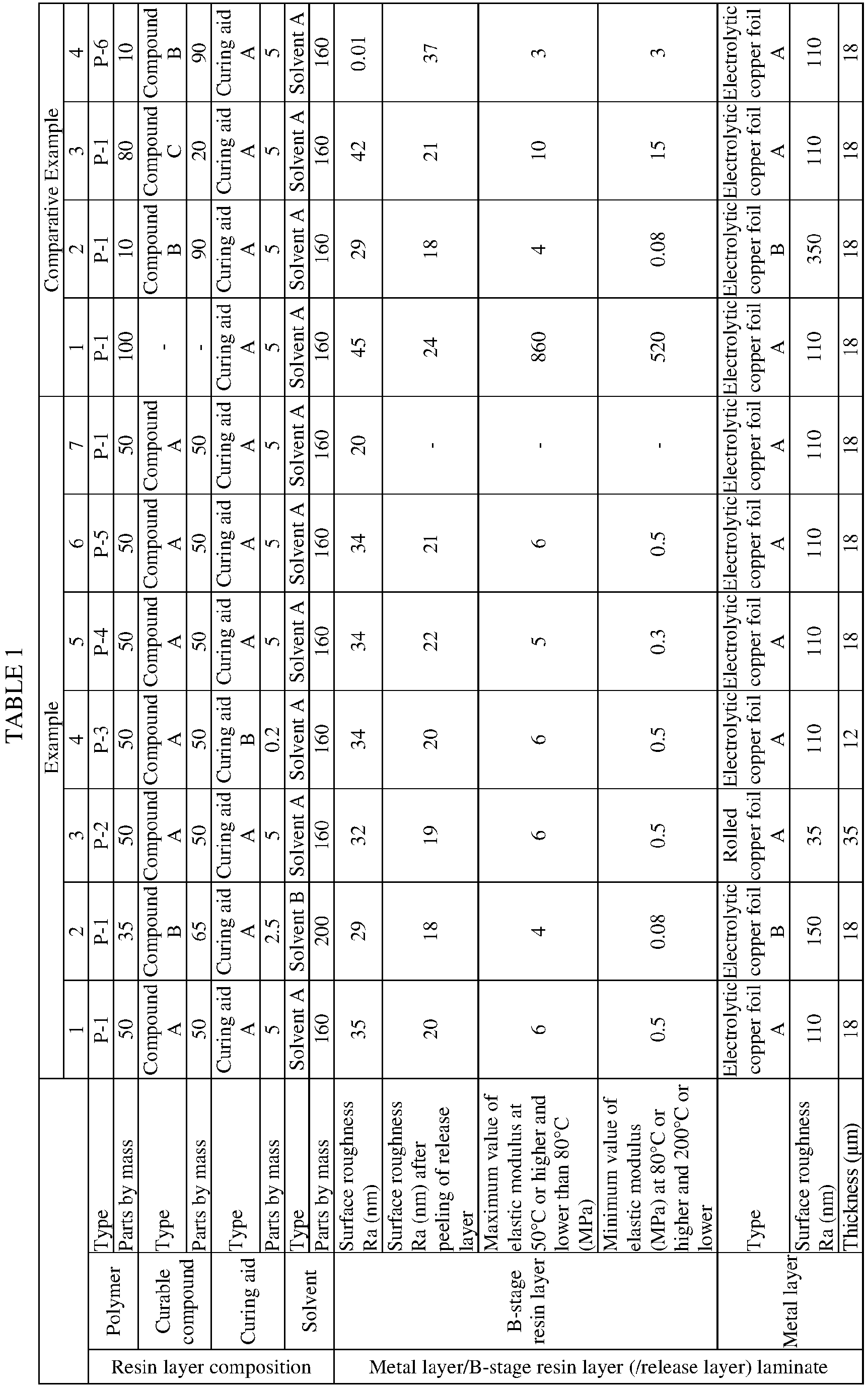

- In Table 1, the following abbreviations are supplemented.
- Polymer
P-6: model number "PPO Resin Powder" available from Sabic, glass transition temperature (Tg): 215°C - Curable compound
- Compound A: 2,2'-bis (4-cyanatophenyl) propane (available from Tokyo Chemical Industry Co., Ltd.)
- Compound B: SR-16H (available from Sakamoto Yakuhin Kogyo Co., Ltd, epoxy equivalent; 160 g/eq)
- Compound C: HP-4032D (available from DIC, epoxy equivalent; 141 meq/g)
- Curing aid
- Curing aid A: 1-benzyl-2-methylimidazole (available from Mitsubishi Chemical Corporation, product name "
BMI 12") - Curing aid B: zinc 2-ethyloctylate (available from Wako Pure Chemical Industries, Ltd.)
- Curing aid A: 1-benzyl-2-methylimidazole (available from Mitsubishi Chemical Corporation, product name "
- Solvent
- Solvent A: Cyclopentanone (available from y Tokyo Chemical Industry Co., Ltd.)
- Solvent B: methylene chloride (available from Tokyo Chemical Industry Co., Ltd.)
- Metal layer type
- Electrolytic copper foil A: product number "TQ-M4-VSP" available from Mitsui Mining & Smelting Co., Ltd.
- Electrolytic copper foil B: product number "3EC-M3S-HTE" available from Mitsui Mining & Smelting Co., Ltd.
- Rolled copper foil A: product number "GHY5-HA" available from JX Nippon Mining & Metals Corporation
The results shown in Table 1 indicates that the circuit boards obtained in Examples 1 to 7 reduced the transmission loss of electric signals in the high-frequency circuit, and had excellent smoothness.
-
- 10.
- Substrate
- 12.
- Resin layer
- 14.
- Metal layer
- 16.
- Wiring portion
- 20.
- Release layer
- 21.
- Resin layer surface (exposed surface)
- 22.
- B-stage resin layer
- 23.
- Resin layer surface (exposed surface)
- 24.
- Metal layer
- 26.
- Metal layer
- 28.
- C-stage resin layer
- 30.
- Metal layer
- 32.
- B-stage resin layer
- 33.
- Resin layer surface (exposed surface)
- 34.
- Metal layer
- 36.
- C-stage resin layer
- 100.
- Circuit board
- 200.
- High-frequency circuit laminate
- 300.
- High-frequency circuit laminate
Claims (6)
- A circuit board comprising a wiring portion and a non-wiring portion,
the wiring portion having a metal layer and a resin layer,
the non-wiring portion having a resin layer,
the resin layer at a frequency 10GHz having a relative permittivity of from 2 to 3 at 23°C,
the circuit board satisfying a relationship:
(A - B)/B ≤ 0.1
wherein A is a maximum value of a thickness in the wiring portion (µm) and B is a minimum value of a thickness in the non-wiring portion (µm). - The circuit board according to claim 1, wherein the metal layer and the resin layer in the wiring portion are laminated in contact with each other.
- The circuit board according to claim 1 or 2, wherein a dielectric loss tangent of the resin layer at a frequency 10 GHz is from 0.001 to 0.01 at 23°C.
- The circuit board according to any one of claims 1 to 3, wherein the resin layer has an elastic modulus of from 0.1 to 3 GPa.
- The circuit board according to any one of claims 1 to 4, wherein a peel strength between the resin layer and the metal layer is 5 N/cm or greater.
- The circuit board according to any one of claims 1 to 5, wherein a thickness of the resin layer is from 10 to 100 µm, and a thickness of the metal layer is from 10 to 50 µm.
Applications Claiming Priority (2)
| Application Number | Priority Date | Filing Date | Title |
|---|---|---|---|
| JP2017177602 | 2017-09-15 | ||
| PCT/JP2018/033480 WO2019054335A1 (en) | 2017-09-15 | 2018-09-10 | PRINTED CIRCUIT BOARD |
Publications (2)
| Publication Number | Publication Date |
|---|---|
| EP3684146A1 true EP3684146A1 (en) | 2020-07-22 |
| EP3684146A4 EP3684146A4 (en) | 2021-06-02 |
Family
ID=65723293
Family Applications (1)
| Application Number | Title | Priority Date | Filing Date |
|---|---|---|---|
| EP18856760.6A Pending EP3684146A4 (en) | 2017-09-15 | 2018-09-10 | Circuit board |
Country Status (7)
| Country | Link |
|---|---|
| US (1) | US11582860B2 (en) |
| EP (1) | EP3684146A4 (en) |
| JP (1) | JP2019054242A (en) |
| KR (1) | KR20200054194A (en) |
| CN (1) | CN111108816A (en) |
| TW (1) | TWI784050B (en) |
| WO (1) | WO2019054335A1 (en) |
Families Citing this family (9)
| Publication number | Priority date | Publication date | Assignee | Title |
|---|---|---|---|---|
| WO2020217700A1 (en) * | 2019-04-25 | 2020-10-29 | Jsr株式会社 | Photosensitive resin composition |
| JP7409374B2 (en) * | 2019-04-25 | 2024-01-09 | Jsr株式会社 | Photosensitive resin composition |
| JP7834649B2 (en) * | 2020-02-13 | 2026-03-24 | 東洋アルミニウム株式会社 | Catalytic metal foil and its applications |
| JP7702778B2 (en) * | 2020-04-27 | 2025-07-04 | 味の素株式会社 | resin composition |
| JP7639824B2 (en) * | 2020-07-28 | 2025-03-05 | 株式会社レゾナック | Method for manufacturing wiring board |
| TW202249544A (en) * | 2021-05-31 | 2022-12-16 | 日商富士軟片股份有限公司 | Wiring board and method for manufacturing wiring board |
| TWI803168B (en) * | 2022-01-25 | 2023-05-21 | 欣興電子股份有限公司 | Method of signal enhancement of circuit of circuit board and structure thereof |
| JP2024018566A (en) * | 2022-07-29 | 2024-02-08 | 長瀬産業株式会社 | Structure |
| US12258445B2 (en) | 2022-11-16 | 2025-03-25 | AGC Multi Material America, Inc. | Curable compositions |
Family Cites Families (61)
| Publication number | Priority date | Publication date | Assignee | Title |
|---|---|---|---|---|
| DE1949137A1 (en) | 1968-09-30 | 1970-04-23 | Procter & Gamble | Optical brighteners and processes for their manufacture |
| US3644285A (en) | 1970-10-12 | 1972-02-22 | Research Corp | Polyaromatic pyrazines |
| US3981832A (en) | 1971-02-11 | 1976-09-21 | Fokker-V.F.W. B.V. | Fire-protecting epoxy resins |
| US3814757A (en) | 1971-04-13 | 1974-06-04 | Du Pont | Diamino substituted dicyano pyrazines and process |
| CH606253A5 (en) | 1977-01-07 | 1978-10-31 | Ciba Geigy Ag | |
| SU858316A1 (en) | 1979-12-17 | 1985-11-30 | Новосибирский институт органической химии СО АН СССР | 2,5-di-(n-aminophenyl)pyramidine as monomer for synthesis of polymides,method of producing same and polyimides on its base as heat resistant material |
| US4931487A (en) | 1988-03-04 | 1990-06-05 | Dow Chemical Company | Chain extenders for polyurethanes |
| US5089571A (en) | 1990-12-04 | 1992-02-18 | The Dow Chemical Company | Regenerated, high molecular weight, thermoplastic resins and process for regenerating thermoplastic resins |
| JPH0565352A (en) | 1991-09-09 | 1993-03-19 | Mitsubishi Gas Chem Co Inc | Production of thermosetting film of cyanate-modified polyphenylene ether resin |
| DE4237768A1 (en) | 1991-11-12 | 1993-05-13 | Ciba Geigy Ag | New polyarylene ether derivs. with reduced viscosity - used to prepare moulded bodies, foils, fibres and membranes, as matrix resins, adhesives or coating agents or as polymer additives |
| JP2001301088A (en) * | 2000-04-24 | 2001-10-30 | Jsr Corp | Laminated film and printed circuit board using the laminated film |
| JP4467816B2 (en) | 2001-02-27 | 2010-05-26 | 株式会社日立製作所 | Low dielectric loss tangent resin composition, curable film, cured product, electrical component using the same, and production method thereof |
| US6869715B2 (en) | 2002-11-23 | 2005-03-22 | Gkss-Forschungszentrum Geesthacht, Gmbh | Ion conductive membrane for electrochemical application |
| JP4211378B2 (en) | 2002-12-13 | 2009-01-21 | ソニー株式会社 | Capacitor element |
| DE602004028614D1 (en) * | 2003-06-19 | 2010-09-23 | Sumitomo Chemical Co | EPOXY COMPOUND AND CURED EPOXY RESIN PRODUCT |
| JP4999285B2 (en) | 2005-05-24 | 2012-08-15 | 上野製薬株式会社 | Liquid crystalline polyester resin composition |
| JP2007262191A (en) | 2006-03-28 | 2007-10-11 | Nippon Steel Chem Co Ltd | Flame-retardant curable resin composition |
| JP2008041960A (en) * | 2006-08-07 | 2008-02-21 | Nissan Chem Ind Ltd | Manufacturing method of electronic circuit components |
| JP2008039703A (en) | 2006-08-09 | 2008-02-21 | Sumitomo Bakelite Co Ltd | Electromagnetic characteristic measuring tool and measuring method |
| JP4963628B2 (en) | 2007-05-15 | 2012-06-27 | 住友化学株式会社 | Polymer film laminate, method for producing the same, and flexible wiring board using polymer film laminate. |
| JP5198105B2 (en) | 2008-03-25 | 2013-05-15 | 日本メクトロン株式会社 | Manufacturing method of multilayer flexible printed wiring board |
| JP4613977B2 (en) | 2008-04-28 | 2011-01-19 | 日立化成工業株式会社 | Prepreg including thin-layer quartz glass cloth and wiring board using the same |
| EP2428529B1 (en) | 2009-05-07 | 2019-03-06 | Nissan Chemical Corporation | Triazine ring-containing polymer and film-forming composition comprising same |
| TWI498408B (en) | 2009-07-14 | 2015-09-01 | Ajinomoto Kk | Attached film with copper foil |
| US8222403B2 (en) | 2009-11-12 | 2012-07-17 | The United States Of America, As Represented By The Secretary Of The Navy | Heteroaromatic phthalonitriles |
| CN102753604B (en) | 2010-01-04 | 2015-01-21 | 罗地亚经营管理公司 | Polyamine and method for producing the same |
| US9185802B2 (en) | 2010-07-26 | 2015-11-10 | Nippon Mektron, Ltd. | Flexible printed circuit board with component mounting section for mounting electronic component and flexible cables extending in different directions from the component mounting section, and method of manufacturing the same |
| JP5511597B2 (en) * | 2010-09-06 | 2014-06-04 | 日東電工株式会社 | Method for manufacturing printed circuit board |
| JP5630182B2 (en) | 2010-09-27 | 2014-11-26 | 株式会社デンソー | Epoxy resin composition and epoxy resin / polyethersulfone composite |
| JP5598258B2 (en) | 2010-10-28 | 2014-10-01 | 日産化学工業株式会社 | Electronic device comprising a triazine ring-containing polymer-containing high refractive index film |
| TWI393495B (en) * | 2010-12-03 | 2013-04-11 | Adv Flexible Circuits Co Ltd | Electrical impedance precision control of signal transmission line for circuit board |
| CN105934104B (en) * | 2010-12-27 | 2019-04-23 | 株式会社可乐丽 | Circuit board and method of manufacturing the same |
| JP5708160B2 (en) * | 2011-04-04 | 2015-04-30 | Jsr株式会社 | Resin substrate for high frequency circuit board and high frequency circuit board |
| US9006339B2 (en) | 2011-05-10 | 2015-04-14 | Basf Se | Mechanically stabilized polyazoles comprising at least one polyvinyl alcohol |
| WO2013027732A1 (en) * | 2011-08-23 | 2013-02-28 | 日本ゼオン株式会社 | Curable resin composition, film, prepreg, laminate, cured product and composite body |
| CN103947306B (en) * | 2011-11-22 | 2017-06-23 | 松下知识产权经营株式会社 | Metal-clad flexible substrate and preparation method thereof |
| WO2013080929A1 (en) | 2011-12-01 | 2013-06-06 | Jsr株式会社 | Resist-underlayer-film-forming composition used in multilayer resist process, resist underlayer film, method for forming same, and pattern-formation method |
| US9596754B2 (en) * | 2011-12-22 | 2017-03-14 | Taiyo Ink Mfg. Co., Ltd. | Dry film, printed wiring board using same, method for producing printed wiring board, and flip chip mounting substrate |
| US8981036B2 (en) | 2012-08-02 | 2015-03-17 | The United States Of America, As Represented By The Secretary Of The Navy | Synthesis of and curing additives for phthalonitriles |
| JP2014070111A (en) * | 2012-09-28 | 2014-04-21 | Nippon Zeon Co Ltd | Insulator, insulating film, laminate, and method for manufacturing laminate |
| WO2014148155A1 (en) | 2013-03-22 | 2014-09-25 | ナミックス株式会社 | Resin composition and adhesive film, coverlay film, and interlayer adhesive using resin composition |
| JP6235787B2 (en) * | 2013-03-29 | 2017-11-22 | 東レ・デュポン株式会社 | Coverlay for high frequency circuit boards |
| WO2015098788A1 (en) | 2013-12-24 | 2015-07-02 | 日産化学工業株式会社 | Triazine-polymer-containing composition |
| CN103801501B (en) * | 2014-01-20 | 2016-04-20 | 中国科学院长春应用化学研究所 | Flexible glue-free copper coated plate and preparation method thereof |
| JP6388483B2 (en) | 2014-03-13 | 2018-09-12 | 東レ・デュポン株式会社 | High frequency circuit board coverlay and flexible flat cable base material |
| JP6432156B2 (en) | 2014-04-28 | 2018-12-05 | Jsr株式会社 | POLYMER COMPOSITION, POLYMER PELLET, MOLDED BODY, AND FILM |
| JP6429267B2 (en) | 2014-04-28 | 2018-11-28 | Jsr株式会社 | Polymer |
| JP5936794B2 (en) * | 2014-06-03 | 2016-06-22 | 三井金属鉱業株式会社 | Metal foil with release resin layer and printed wiring board |
| JP6206445B2 (en) | 2014-07-25 | 2017-10-04 | Jsr株式会社 | Circuit board resin substrate, circuit board resin composition, and circuit board |
| JP2016087799A (en) | 2014-10-29 | 2016-05-23 | 東レ・デュポン株式会社 | Long-sized laminate for high frequency circuit board, and method for manufacturing the same |
| KR101832684B1 (en) | 2015-01-13 | 2018-02-26 | 히타치가세이가부시끼가이샤 | A resin film for a flexible printed wiring board, a metal foil with a resin, a coverlay film, a bonding sheet and a flexible printed wiring board |
| WO2016143447A1 (en) | 2015-03-11 | 2016-09-15 | Jsr株式会社 | Polymer, resin composition and resin molded body |
| WO2017007928A1 (en) | 2015-07-07 | 2017-01-12 | Katz Jeffrey Louis | Polymeric ion conductor with improved thermal characteristics |
| JP6590568B2 (en) | 2015-07-22 | 2019-10-16 | 株式会社カネカ | Insulating film, method for producing insulating film, and method for producing metal-clad laminate |
| JP6927665B2 (en) * | 2015-12-25 | 2021-09-01 | 日東電工株式会社 | Wiring circuit board |
| JP6888308B2 (en) | 2016-02-04 | 2021-06-16 | Jsr株式会社 | Resin composition, polymer production method and molded product |
| JP6971580B2 (en) | 2016-02-12 | 2021-11-24 | 株式会社カネカ | Multilayer polyimide film and flexible metal-clad laminate |
| JP6866737B2 (en) | 2016-04-20 | 2021-04-28 | Jsr株式会社 | Polymers, compositions and moldings |
| KR102267304B1 (en) * | 2016-04-20 | 2021-06-21 | 제이에스알 가부시끼가이샤 | Polymers, compositions, molded articles, cured articles and laminates |
| WO2017209208A1 (en) | 2016-06-02 | 2017-12-07 | 日立化成株式会社 | Production method for laminate |
| JP6922364B2 (en) | 2016-07-28 | 2021-08-18 | Jsr株式会社 | Polymers, compositions and moldings |
-
2018
- 2018-09-10 CN CN201880058828.9A patent/CN111108816A/en active Pending
- 2018-09-10 EP EP18856760.6A patent/EP3684146A4/en active Pending
- 2018-09-10 US US16/647,350 patent/US11582860B2/en active Active
- 2018-09-10 KR KR1020207007170A patent/KR20200054194A/en not_active Ceased
- 2018-09-10 JP JP2018168775A patent/JP2019054242A/en active Pending
- 2018-09-10 WO PCT/JP2018/033480 patent/WO2019054335A1/en not_active Ceased
- 2018-09-14 TW TW107132490A patent/TWI784050B/en active
Also Published As
| Publication number | Publication date |
|---|---|
| JP2019054242A (en) | 2019-04-04 |
| US11582860B2 (en) | 2023-02-14 |
| WO2019054335A1 (en) | 2019-03-21 |
| US20200344870A1 (en) | 2020-10-29 |
| KR20200054194A (en) | 2020-05-19 |
| TWI784050B (en) | 2022-11-21 |
| EP3684146A4 (en) | 2021-06-02 |
| CN111108816A (en) | 2020-05-05 |
| TW201921505A (en) | 2019-06-01 |
Similar Documents
| Publication | Publication Date | Title |
|---|---|---|
| US11582860B2 (en) | Circuit board | |
| US11134568B2 (en) | High-frequency circuit laminate and method for producing same, and B-stage sheet | |
| TWI784927B (en) | resin composition | |
| KR102780208B1 (en) | Laminate for high-frequency circuit and its manufacturing method, flexible printed substrate, B-stage sheet, and laminate roll | |
| JP7047257B2 (en) | Resin composition | |
| TW201900768A (en) | Resin composition | |
| JP7115165B2 (en) | Laminates for high-frequency circuits and flexible printed circuit boards | |
| JP6911806B2 (en) | Resin composition, sheet-like laminated material, printed wiring board and semiconductor device | |
| TW201718688A (en) | Resin composition | |
| US20230391949A1 (en) | Polyester resin | |
| JP7087859B2 (en) | Laminated body wound body | |
| US20040265609A1 (en) | Metal-clad laminate | |
| KR102065643B1 (en) | Flexible Copper Clad Layer and manufacturing method thereof | |
| JP2005053940A (en) | Adhesive composition for semiconductor device and coverlay film, adhesive sheet, copper-clad polyimide film using the same | |
| JP2020074444A (en) | Adhesive film, print circuit board and semiconductor device | |
| JP2020029566A (en) | Resin composition | |
| JP2024112016A (en) | Resin composition | |
| KR20170099664A (en) | Flexible circuit clad laminate, printed circuit board using it, and method of manufacturing the same |
Legal Events
| Date | Code | Title | Description |
|---|---|---|---|
| STAA | Information on the status of an ep patent application or granted ep patent |
Free format text: STATUS: THE INTERNATIONAL PUBLICATION HAS BEEN MADE |
|
| PUAI | Public reference made under article 153(3) epc to a published international application that has entered the european phase |
Free format text: ORIGINAL CODE: 0009012 |
|
| STAA | Information on the status of an ep patent application or granted ep patent |
Free format text: STATUS: REQUEST FOR EXAMINATION WAS MADE |
|
| 17P | Request for examination filed |
Effective date: 20200326 |
|
| AK | Designated contracting states |
Kind code of ref document: A1 Designated state(s): AL AT BE BG CH CY CZ DE DK EE ES FI FR GB GR HR HU IE IS IT LI LT LU LV MC MK MT NL NO PL PT RO RS SE SI SK SM TR |
|
| AX | Request for extension of the european patent |
Extension state: BA ME |
|
| DAV | Request for validation of the european patent (deleted) | ||
| DAX | Request for extension of the european patent (deleted) | ||
| A4 | Supplementary search report drawn up and despatched |
Effective date: 20210504 |
|
| RIC1 | Information provided on ipc code assigned before grant |
Ipc: H05K 1/03 20060101AFI20210428BHEP Ipc: B32B 15/08 20060101ALI20210428BHEP Ipc: H05K 3/28 20060101ALI20210428BHEP Ipc: H05K 3/46 20060101ALI20210428BHEP Ipc: H05K 3/38 20060101ALI20210428BHEP |
|
| RAP1 | Party data changed (applicant data changed or rights of an application transferred) |
Owner name: JICC-02 CO., LTD. |
|
| RAP3 | Party data changed (applicant data changed or rights of an application transferred) |
Owner name: JSR CORPORATION |