EP3680938B1 - Spinstrom-magnetisierungsumkehrelement und magnetwiderstandseffektelement vom spin-orbit-drehmomenttyp - Google Patents
Spinstrom-magnetisierungsumkehrelement und magnetwiderstandseffektelement vom spin-orbit-drehmomenttyp Download PDFInfo
- Publication number
- EP3680938B1 EP3680938B1 EP18854094.2A EP18854094A EP3680938B1 EP 3680938 B1 EP3680938 B1 EP 3680938B1 EP 18854094 A EP18854094 A EP 18854094A EP 3680938 B1 EP3680938 B1 EP 3680938B1
- Authority
- EP
- European Patent Office
- Prior art keywords
- spin
- region
- orbit torque
- ferromagnetic layer
- spin orbit
- Prior art date
- Legal status (The legal status is an assumption and is not a legal conclusion. Google has not performed a legal analysis and makes no representation as to the accuracy of the status listed.)
- Active
Links
Images


Classifications
-
- G—PHYSICS
- G11—INFORMATION STORAGE
- G11C—STATIC STORES
- G11C11/00—Digital stores characterised by the use of particular electric or magnetic storage elements; Storage elements therefor
- G11C11/02—Digital stores characterised by the use of particular electric or magnetic storage elements; Storage elements therefor using magnetic elements
- G11C11/16—Digital stores characterised by the use of particular electric or magnetic storage elements; Storage elements therefor using magnetic elements using elements in which the storage effect is based on magnetic spin effect
- G11C11/161—Digital stores characterised by the use of particular electric or magnetic storage elements; Storage elements therefor using magnetic elements using elements in which the storage effect is based on magnetic spin effect details concerning the memory cell structure, e.g. the layers of the ferromagnetic memory cell
-
- H—ELECTRICITY
- H10—SEMICONDUCTOR DEVICES; ELECTRIC SOLID-STATE DEVICES NOT OTHERWISE PROVIDED FOR
- H10N—ELECTRIC SOLID-STATE DEVICES NOT OTHERWISE PROVIDED FOR
- H10N52/00—Hall-effect devices
- H10N52/80—Constructional details
-
- H—ELECTRICITY
- H03—ELECTRONIC CIRCUITRY
- H03B—GENERATION OF OSCILLATIONS, DIRECTLY OR BY FREQUENCY-CHANGING, BY CIRCUITS EMPLOYING ACTIVE ELEMENTS WHICH OPERATE IN A NON-SWITCHING MANNER; GENERATION OF NOISE BY SUCH CIRCUITS
- H03B15/00—Generation of oscillations using galvano-magnetic devices, e.g. Hall-effect devices, or using superconductivity effects
-
- H—ELECTRICITY
- H10—SEMICONDUCTOR DEVICES; ELECTRIC SOLID-STATE DEVICES NOT OTHERWISE PROVIDED FOR
- H10B—ELECTRONIC MEMORY DEVICES
- H10B61/00—Magnetic memory devices, e.g. magnetoresistive RAM [MRAM] devices
-
- H—ELECTRICITY
- H10—SEMICONDUCTOR DEVICES; ELECTRIC SOLID-STATE DEVICES NOT OTHERWISE PROVIDED FOR
- H10D—INORGANIC ELECTRIC SEMICONDUCTOR DEVICES
- H10D48/00—Individual devices not covered by groups H10D1/00 - H10D44/00
- H10D48/40—Devices controlled by magnetic fields
-
- H—ELECTRICITY
- H10—SEMICONDUCTOR DEVICES; ELECTRIC SOLID-STATE DEVICES NOT OTHERWISE PROVIDED FOR
- H10N—ELECTRIC SOLID-STATE DEVICES NOT OTHERWISE PROVIDED FOR
- H10N50/00—Galvanomagnetic devices
- H10N50/10—Magnetoresistive devices
-
- H—ELECTRICITY
- H10—SEMICONDUCTOR DEVICES; ELECTRIC SOLID-STATE DEVICES NOT OTHERWISE PROVIDED FOR
- H10N—ELECTRIC SOLID-STATE DEVICES NOT OTHERWISE PROVIDED FOR
- H10N50/00—Galvanomagnetic devices
- H10N50/80—Constructional details
-
- H—ELECTRICITY
- H10—SEMICONDUCTOR DEVICES; ELECTRIC SOLID-STATE DEVICES NOT OTHERWISE PROVIDED FOR
- H10N—ELECTRIC SOLID-STATE DEVICES NOT OTHERWISE PROVIDED FOR
- H10N50/00—Galvanomagnetic devices
- H10N50/80—Constructional details
- H10N50/85—Materials of the active region
-
- H—ELECTRICITY
- H10—SEMICONDUCTOR DEVICES; ELECTRIC SOLID-STATE DEVICES NOT OTHERWISE PROVIDED FOR
- H10N—ELECTRIC SOLID-STATE DEVICES NOT OTHERWISE PROVIDED FOR
- H10N52/00—Hall-effect devices
-
- H—ELECTRICITY
- H10—SEMICONDUCTOR DEVICES; ELECTRIC SOLID-STATE DEVICES NOT OTHERWISE PROVIDED FOR
- H10N—ELECTRIC SOLID-STATE DEVICES NOT OTHERWISE PROVIDED FOR
- H10N52/00—Hall-effect devices
- H10N52/01—Manufacture or treatment
Definitions
- the present invention relates to a spin-current magnetization rotational element and a spin orbit torque type magnetoresistance effect element.
- a giant magnetoresistance (GMR) element that is configured by a multilayer film including a ferromagnetic layer and a non-magnetic layer and a tunneling magnetoresistance (TMR) element that uses an insulating layer (a tunnel barrier layer, a barrier layer) as a non-magnetic layer is known as a magnetoresistance effect element.
- TMR tunneling magnetoresistance
- the TMR element has a higher element resistance and a larger magnetoresistance (MR) ratio than the GMR element. For that reason, attention is focused on the TMR element as an element for magnetic sensors, high-frequency components, magnetic heads and nonvolatile random-access memories (MRAM).
- the MRAM reads and writes data by utilizing the characteristic that the element resistance of the TMR element changes as the direction of magnetization of two ferromagnetic layers sandwiching the insulating layer changes.
- a writing method of MRAM a method in which writing (magnetization rotational) is performed by utilizing a magnetic field created by an electric current and a method in which writing (magnetization rotational) is performed by using a spin-transfer torque (STT) generated by applying an electric current in a laminating direction of a magnetoresistance effect element are known.
- STT spin-transfer torque
- the rotational current density for the magnetization rotational is high. It is desirable that the rotational current density be low from the viewpoint of long life span of the TMR element. This also applies to the GMR element.
- Non-Patent Literature 1 a pure spin-current generated by spin-orbit interaction, which performs magnetization rotational by a mechanism different from STT.
- SOT spin orbit torque
- Pure spin-current is generated by the same number of spin up and spin down electrons flowing in opposite directions, and the flow of electric charge is canceled out. For that reason, electric current flowing through the magnetoresistance effect element is zero, and it is expected that the magnetoresistance effect element has a long life span.
- Other prior art in this context is further referred to below (see Literature 2 to 6)
- the present invention has been made in view of the above circumstances, and it is an object of the present invention to provide a spin-current magnetization rotational element and a spin orbit torque type magnetoresistance effect element capable of efficiently removing impurities adhered to a side wall.
- the present inventors have found that impurities can be suppressed from reattachment to a side wall by relatively lowering the position of a second region outside a first region in which a ferromagnetic layer is laminated. That is, the present invention provides the following means to solve the above-mentioned problems.
- FIG 1 is a perspective view schematically showing a spin-current magnetization rotational element according to a first embodiment of the present invention.
- FIG 2 is a cross-sectional view schematically showing the spin-current magnetization rotational element according to the first embodiment.
- the spin-current magnetization rotational element 10 according to the first embodiment includes a first ferromagnetic layer 1 and a spin orbit torque wiring 2.
- a first direction in which the spin orbit torque wiring 2 extends is defined as an x direction
- a laminating direction (a second direction) of the first ferromagnetic layer 1 is defined as a z direction
- a direction orthogonal to both of the x direction and the z direction is defined as a y direction.
- the first ferromagnetic layer 1 is disposed (placed) to stand upright in the second direction (the z direction) intersecting the first direction (the x direction) of the spin orbit torque wiring 2.
- a thickness direction of the first ferromagnetic layer 1 may be substantially parallel to the z direction.
- the first ferromagnetic layer 1 functions by changing the direction of its magnetization M1.
- the first ferromagnetic layer 1 is an in-plane magnetized film in which the magnetization M1 is oriented in the x direction in FIG 1 , it may be an in-plane magnetized film oriented in a different direction in the xy plane and may be a perpendicular magnetized film oriented in the z direction.
- a ferromagnetic material particularly, a soft magnetic material
- metals selected from the group consisting of Cr, Mn, Co, Fe and Ni, alloys containing at least one of the above metals, and alloys containing the above metals and at least one element of B, C, and N, or the like can be used.
- Co-Fe, Co-Fe-B, and Ni-Fe can be exemplified.
- a Heusler alloy such as Co 2 FeSi may be used as the first ferromagnetic layer 1.
- the Heusler alloy contains an intermetallic compound having a chemical composition of X 2 YZ, in which X is a transition metal element of Co, Fe, Ni, or Cu group or a noble metal element on the periodic table, Y is a transition metal of Mn, V, Cr or Ti group or an element of X, and Z is a typical element of group III to group V.
- Co 2 FeSi, Co 2 FeGe, Co 2 FeGa, Co 2 MnSi, Co 2 Mn 1-a Fe a Al b Si 1-b , Co 2 FeGe 1-c Ga c and the like can be exemplified.
- the spin orbit torque wiring 2 extends in the x direction.
- the spin orbit torque wiring 2 is connected to one surface of the first ferromagnetic layer 1 in the z direction.
- the spin orbit torque wiring 2 may be directly connected to the first ferromagnetic layer 1 or may be connected via another layer.
- the spin orbit torque wiring 2 is made of a material in which a pure spin-current is generated due to the Spin Hall effect when a current flows. As such a material, any material may be used as long as a pure spin-current is generated in the spin orbit torque wiring 2. Therefore, the spin orbit torque wiring 2 may not be necessarily made of a single element and may be made of a plurality of materials, for example, such as a material which easily generates a pure spin-current and a material which hardly generates a pure spin-current.
- the Spin Hall effect is a phenomenon in which, when an electric current flows in a material, a pure spin-current is induced in a direction orthogonal to the direction of current due to the interaction (the spin-orbit interaction) acting between the orbital angular momentum and the spin angular momentum of electrons responsible for the current.
- the mechanism by which a pure spin-current is induced by the Spin Hall effect will be described.
- the number of electrons of the first spin S1 is equal to the number of electrons of the second spin S2 in a non-magnetic material (a material that is not a ferromagnetic material)
- the number of electrons of the first spin S1 oriented upward is equal to the number of electrons of the second spin S2 oriented downward in the drawings.
- the electric current as a net flow of charge is zero.
- This spin-current which is not accompanied by the electric current is particularly called pure spin-current.
- the phenomenon in which the first spin S1 and the second spin S2 are bent in opposite directions is the same as the non-magnetic material.
- either one of the first spin S1 and the second spin S2 is large, and as a result, a net flow of charge occurs (voltage is generated). Therefore, as a material of the spin orbit torque wiring 2, a material only consisting of a ferromagnetic material is not included.
- the pure spin-current JS flows in the z direction in the drawings.
- JS is a flow of electrons with a polarizability of 100%.
- FIG 1 when a ferromagnetic material is brought into contact with an upper surface of the spin orbit torque wiring 2, the pure spin-current diffuses and flows into the ferromagnetic material. That is, spin is injected into the first ferromagnetic layer 1.
- the spin orbit torque wiring 2 is configured by any one of a metal, an alloy, an intermetallic compound, a metal boride, a metal carbide, a metal silicide, and a metal phosphide which has a function of generating a pure spin-current by a Spin Hall effect when an electric current flows.
- the main constituent material of the spin orbit torque wiring 2 may be a non-magnetic heavy metal.
- the heavy metal means a metal having a specific gravity equal to or higher than yttrium.
- the non-magnetic heavy metal may be a non-magnetic metal having a large atomic number, that is, a non-magnetic metal having an atomic number of 39 or more and having d electrons or f electrons in the outermost shell. In such a non-magnetic metal, the spin-orbit interaction causing the Spin Hall effect is large.
- the spin orbit torque wiring 2 may contain a magnetic metal.
- the magnetic metal means a ferromagnetic metal or an antiferromagnetic metal. If a small amount of magnetic metal is contained in the non-magnetic metal, it becomes a scattering factor of spin. If the spin is scattered, the spin-orbit interaction is enhanced and the spin-current generation efficiency with respect to the current is increased.
- the main configuration of the spin orbit torque wiring 2 may be made of only an antiferromagnetic metal.
- the molar ratio of the added magnetic metal may be sufficiently smaller than the total molar ratio of the elements constituting the spin orbit torque wiring.
- the molar ratio of the added magnetic metal may be 3% or less.
- the spin orbit torque wiring 2 may include a topological insulator.
- the main configuration of the spin orbit torque wiring 2 may be a topological insulator.
- the topological insulator is a material in which the inside of the substance is an insulator or a high resistance body, a spin-polarized metallic state is generated on the surface. An internal magnetic field is generated in this material by the spin-orbit interaction. As a result, even if there is no external magnetic field, a new topological phase develops due to the effect of the spin-orbit interaction. This is a topological insulator, and, due to strong spin orbital interaction and breaking of inversion symmetry at the edge, pure spin-current can be generated with high efficiency.
- topological insulator for example, SnTe, Bi 1.5 Sb 0.5 Te 1.7 Se 1.3 , TlBiSe 2 , Bi 2 Te 3 , Bi 1-x Sb x , (Bi 1-x Sb x ) 2 Te 3 and the like may be used. These topological insulators are capable of generating spin-current with high efficiency.
- the spin orbit torque wiring 2 has a first surface 2a positioned on the side where the first ferromagnetic layer 1 is arranged (laminated) and a second surface 2b on the side opposite to the first surface 2a.
- the first surface 2a has a first region 2A, in which the first ferromagnetic layer 1 is disposed, and a second region 2B positioned outside the first region 2A and recessed in the -z direction (second surface 2b side) from the first region 2A.
- the second region 2B is positioned on an outer region in the +x direction and on an outer region in the -x direction when viewed from the first region 2A. That is, the first region 2A is sandwiched by a plurality of second regions 2B in the x direction.
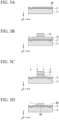
- FIGS. 3A to 3D are schematic diagrams explaining an example of a method for manufacturing the spin-current magnetization rotational element 10.
- a substrate 11 having a plurality (two in this case) of recessed portions 2B aligned in one direction (x direction) on one main surface is prepared, and a layer (layer made of a member for spin orbit torque wiring) serving as a base of the spin orbit torque wiring is formed (laminated) on one main surface of the substrate 11.
- a lamination method known methods such as a sputtering method and a chemical vapor deposition (CVD) method can be used.
- the layer serving as the base of the spin orbit torque wiring is processed to extend along the x direction while covering the plurality of recessed portions 2B by using a technique such as photolithography to form the spin orbit torque wiring 2. Since the spin orbit torque wiring 2 is formed to follow the shape of the surface of the substrate 11, the second region 2B can be produced by providing corresponding recessed portions in the substrate 11 ( FIG. 3A ).
- an insulating layer is coated to surround a periphery of the spin orbit torque wiring.
- an oxide film, a nitride film, or the like can be used as the insulating layer.
- the surface of the insulating layer and the spin orbit torque wiring 2 is planarized by chemical mechanical polishing (CMP).
- CMP chemical mechanical polishing
- a layer (layer made of a material for the first ferromagnetic layer) 12 serving as the base of the first ferromagnetic layer is formed, and a protective layer 13 made of a resist or the like is formed on the layer 12 serving as the base of the first ferromagnetic layer ( FIG. 3B ).
- methods such as reactive ion etching (RIE) and ion beam etching (IBE) can be used ( FIG. 3C ).
- Impurities may attach to the side wall of the first ferromagnetic layer 1 during processing. These impurities deteriorate magnetic properties of the first ferromagnetic layer 1. Attached impurities can be removed by irradiating the ion beam from the side wall ( FIG. 3D ). An incident angle of the ion beam (the angle formed by the traveling direction of the ion beam and the xy plane) may be close to parallel to the xy plane. The angle formed by the traveling direction of the incident beam and the xy plane is tilted to 10°.
- the side wall of the first ferromagnetic layer 1 becomes a shadow of the second region 2B and the ion beam cannot be efficiently irradiated to the side wall of the first ferromagnetic layer 1.
- the second region 2B is recessed from the first region 2A on the first surface 2a, the second region 2B does not inhibit the ion beam incident on the first ferromagnetic layer 1. That is, it is possible to irradiate the side wall of the first ferromagnetic layer 1 directly with the ion beam so that impurities can be removed efficiently.
- the recessed portion of the second region 2B shown in FIG 2 is configured by a first inclined surface 2B1 and a second inclined surface 2B2.
- the first inclined surface 2B 1 is an inclined surface inclined with respect to the first region 2A of the first surface 2a to be deeper the further away it is from the first region 2A.
- the second inclined surface 2B2 is an inclined surface inclined with respect to the first region 2A of the first surface 2a to be deeper the closer it is to the first region 2A.
- by providing the first inclined surface 2B1 in the second region 2B by providing the first inclined surface 2B1 in the second region 2B, reattachment of the impurities from the spin orbit torque wiring 2 can be suppressed.
- a protruding portion following the shape of the recessed portion is formed on the side opposite to the first surface 2a is shown, but this protruding portion is not essential.
- the ion beam is incident at an angle with respect to the xy plane. Therefore, a part of the ion beam is incident on the spin orbit torque wiring 2.
- a part of the spin orbit torque wiring 2 is scattered. The scattered matter reattaches to the side wall of the first ferromagnetic layer 1. Since the spin orbit torque wiring 2 has conductivity, the scattered matter which has scattered and reattached becomes an impurity which deteriorates the magnetic characteristics of the first ferromagnetic layer 1.
- FIGS. 4A and 4B are diagrams schematically showing the scattering direction of impurities generated by the ion beam incident on the flat surface and the scattering direction of the impurity generated by the ion beam incident on the first inclined surface.
- the scattered direction of the scattered matter S is at an angle ⁇ with respect to the flat surface F1.
- the scattering direction of the scattering matter S is an angle ⁇ +2 ⁇ with respect to the surface F2.
- ⁇ is the inclination angle of the first inclined surface 2B1
- the plane F2 is a plane parallel to the horizontal plane extending from the end on the second region 2B side of the first region 2A and also parallel to the flat face F1.
- the first inclined surface 2B1 can tilt the scattering direction of the scattering object S in the +z direction (upward).
- the height (thickness) h of the first ferromagnetic layer 1 is finite. Therefore, the scattering direction of the scattering object S is tilted in the +z direction (upward) so that the amount of the scattering matter S adhering to the first ferromagnetic layer 1 can be reduced.
- the relational equation of G>h/tan( ⁇ +2 ⁇ ) is satisfied.
- G corresponds to the shortest distance between the first region 2A and the second region 2B. Since this relationship is satisfied, the scattering material S splashed on the first inclined surface 2B1 passes over the end (top) in the +z direction (upward) of the first ferromagnetic layer 1 so that the amount of impurities reattached to the first ferromagnetic layer 1 can be reduced.
- the incident angle is set to 10°.
- the inclination angle ⁇ of the first inclined surface 2B1 may be large.
- the positional relationship between the first region 2A and the second region 2B in the z direction greatly fluctuates, which makes it difficult to uniformly manufacture the spin orbit torque wiring 2.
- the thickness of the spin orbit torque wiring 2 formed in the second region 2B becomes thinner and the spin orbit torque wiring 2 may break. Therefore, the depth of the recessed portion of the second region 2B with respect to the first region 2A may be less than or equal to the thickness of the spin orbit torque wiring 2.
- the spin-current magnetization rotational element 10 of the present embodiment it is possible to efficiently remove impurities adhering to the side wall of the first ferromagnetic layer 1. By removing impurities, the magnetic characteristics of the first ferromagnetic layer 1 are stabilized. Further, by providing the first inclined surface 2B1 in the second region 2B, reattachment of impurities from the spin orbit torque wiring 2 can be suppressed.
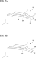
- FIGS. 5A and 5B are perspective views schematically showing another example of the spin-current magnetization rotational element according to exemplary embodiments which are not part of the present invention.
- the spin orbit torque wiring 22 shown in FIG. 5A includes a first portion 24 including a first region 22A and a second portion 26 including a second region 22B. Since the second portion 26 is positioned in the -z direction (downward) with respect to the first portion 24, the second region 22B is recessed in the -z direction with respect to the first region 22A.
- the shape of the spin orbit torque wiring 32 is different from that of the spin orbit torque wiring 2 applied to the spin-current magnetization rotational element 10 according to the first embodiment.
- the spin orbit torque wiring 32 shown in FIG. 5B consists only of the inclined surface, which is inclined so that the second region 32B is deeper in the -z direction the further away the second region 32B is from the first region 32A.
- the second region 32B is recessed in the z direction with respect to the first region 32A.
- the second regions 2B, 22B, and 32B presented above are all positioned in the x direction with respect to the first regions 2A, 22A, and 32A.
- the second region is not limited to the position in the x direction with respect to the first region but may be the position in the y direction.
- the spin orbit torque wiring 2 extends in the x direction. That is, the insulating layer expands to the side of the y direction of the first ferromagnetic layer 1. When the scattered matter generated by the ion beam is an insulator, the scattered matter has little influence on the magnetic characteristics of the first ferromagnetic layer 1.
- the second region may be positioned on the side in the x direction of the first region.
- the first ferromagnetic layer 1 and the spin orbit torque wiring 2 may have the same width in the y direction.
- the metal is scattered by the ion beam from the y direction.
- the occurrence of this problem can be suppressed by aligning the widths of the first ferromagnetic layer 1 and the spin orbit torque wiring 2.
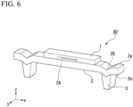
- FIG. 6 is a schematic perspective view of a spin-current magnetization rotational element 40 according to a second embodiment of the present invention.
- the spin-current magnetization rotational element 40 is different from the spin-current magnetization rotational element 10 according to the first embodiment in that the spin-current magnetization rotational element 40 has a via wiring 3.
- the other configurations are the same as those of the spin-current magnetization rotational element 10 according to the first embodiment, and the corresponding components are denoted by the same reference numerals.
- the via wiring 3 extends along the second direction (z direction) intersecting the first direction (x direction) from the second surface 2b on the opposite side to the first surface 2a in the surface of the spin orbit torque wiring 2.
- the via wiring 3 is a connection wiring for allowing a current to flow in the x direction in which the spin orbit torque wiring 2 extends.
- the second region 2B is positioned at a position overlapping the via wiring 3 when viewed from the z direction (in plan view from the second direction).
- the second region 2B of the first surface 2a can be easily recessed with respect to the first region 2A.
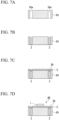
- FIGS. 7A to 7D are diagrams schematically showing an example of a method of manufacturing the spin-current magnetization rotational element 40 having the via wiring 3.
- an opening 50a extending in the z direction is provided in the interlayer insulating film 50 formed on the second surface 2b of the spin orbit torque wiring 2 ( FIG. 7A ).
- a metal is laminated (buried) in the opening 50a, and a via wiring 3 is formed ( FIG. 7B ).
- the length of the via wiring 3 is adjusted to be shorter than the thickness of the interlayer insulating film 50.
- a layer (a member for spin orbit torque wiring) serving as the base of the spin orbit torque wiring is laminated (disposed) on an interlayer insulating film 50 and the via wiring 3, and the layer is processed into the spin orbit torque wiring 2 ( FIG. 7C ). Since the via wiring 3 is recessed in the thickness direction of the interlayer insulating film 50, the spin orbit torque wiring 2 also follows its shape. As a result, the position in the xy plane of the second region 2B of the spin orbit torque wiring 2 coincides with the position in the xy plane of the via wiring 3, and the second region 2B and the via wiring 3 overlap when viewed from the z direction. After the second region 2B recessed from the first region 2A is formed on the first surface 2a, the spin-current magnetization rotational element 40 can be manufactured by the same procedure as in FIG. 3 ( FIG. 7D ).
- the spin-current magnetization rotational element 40 of the present embodiment it is possible to easily recess the second region 2B with respect to the first region 2A in the process of manufacturing the via wiring 3. Further, impurities adhering to the side walls of the first ferromagnetic layer 1 can be efficiently removed by depressing the second region 2B with respect to the first region 2A.
- FIG. 8 is a schematic sectional view of a spin orbit torque type magnetoresistance effect element 100 according to a third embodiment of the present invention.
- the spin orbit torque type magnetoresistance effect element 100 shown in FIG. 8 includes a first ferromagnetic layer 1, a spin orbit torque wiring 2, a via wiring 3, a non-magnetic layer 5, a second ferromagnetic layer 6, and a mask layer 7.
- the laminate configured by the first ferromagnetic layer 1, the spin orbit torque wiring 2 and the via wiring 3 corresponds to the spin-current magnetization rotational element 40 according to the second embodiment shown in FIG. 6 .
- the non-magnetic layer 5 is disposed on the side of the surface of the first ferromagnetic layer 1 opposite to the surface positioned on the side of the spin orbit torque wiring 2.
- the second ferromagnetic layer 6 is disposed on the non-magnetic layer 5 to sandwich the non-magnetic layer 5 between the second ferromagnetic layer 6 and the first ferromagnetic layer 1.
- the spin-current magnetization rotational elements 10, 20, and 30 according to the first embodiment may be used. A description of the same configuration as that of the spin-current magnetization rotational element 40 of the second embodiment will be omitted.
- the laminated body (a functional section 60), in which the first ferromagnetic layer 1, the non-magnetic layer 5, and the second ferromagnetic layer 6 are laminated, functions in the same manner as an ordinary magnetoresistance effect element.
- the functional section 60 functions due to the magnetization M6 of the second ferromagnetic layer 6 being fixed in one direction (z direction) and the direction of the magnetization M1 of the first ferromagnetic layer 1 being relatively changed.
- this functional section 60 is applied to a coercive force difference type (pseudo spin valve type) magnetoresistive random-access memory (MRAM)
- MRAM magnetoresistive random-access memory
- the coercive force of the second ferromagnetic layer 6 is made to be larger than the coercive force of the first ferromagnetic layer 1.
- an exchange bias type spin valve type
- the magnetization M6 of the second ferromagnetic layer 6 is fixed by exchange coupling with the antiferromagnetic layer.
- the functional section 60 has the same structure as a tunneling magnetoresistance (TMR) element, and when the functional section 60 is made of a metal, it has the same configuration as the giant magnetoresistance (GMR) device.
- TMR tunneling magnetoresistance
- GMR giant magnetoresistance
- each layer may be configured by a plurality of layers or may be provided with another layer such as an antiferromagnetic layer for fixing the magnetization direction of the second ferromagnetic layer 6.
- the second ferromagnetic layer 6 is called a fixed layer or a reference layer
- the first ferromagnetic layer 1 is called a free layer, a memory layer, or the like.
- a known material can be used for the material of the second ferromagnetic layer 6.
- a metal selected from the group consisting of Cr, Mn, Co, Fe and Ni, and an alloy exhibiting ferromagnetism containing at least one of these metals can be used.
- An alloy containing these metals and at least one element of B, C, and N can be used.
- Co-Fe and Co-Fe-B can be exemplified.
- a Heusler alloy such as Co 2 FeSi may be used as the material of the second ferromagnetic layer 6.
- the Heusler alloy contains an intermetallic compound having a chemical composition of X 2 YZ, in which X is a transition metal element of Co, Fe, Ni, or Cu group or a noble metal element in the periodic table, Y is a transition metal of Mn, V, Cr or Ti group or an elemental species of X, and Z is a typical element of group III to group V.
- Co 2 FeSi, Co 2 FeGe, Co 2 FeGa, Co 2 MnSi, Co 2 Mn 1-a Fe a Al b Si 1-b , Co 2 FeGe 1-c Ga c and the like can be exemplified.
- an antiferromagnetic material such as IrMn, PtMn or the like may be used as a material in contact with the second ferromagnetic layer 6.
- a synthetic ferromagnetic coupling structure may be adopted.
- the non-magnetic layer 5 a known material can be used.
- the non-magnetic layer 5 is made of an insulator (in the case of a tunnel barrier layer)
- Al 2 O 3 , SiO 2 , MgO, MgAl 2 O 4 , or the like can be used as a material thereof.
- a material in which an Al, Si, or Mg part is substituted with Zn, Be, or the like can also be used.
- MgO and MgAl 2 O 4 are materials that can realize coherent tunneling, spin can be efficiently injected.
- the non-magnetic layer 5 is made of a metal
- Cu, Au, Ag, or the like can be used as the material thereof.
- the non-magnetic layer 5 is made of a semiconductor, Si, Ge, CuInSe 2 , CuGaSe 2 , Cu(In, Ga)Se 2 , or the like can be used as a material thereof.
- the functional section 60 may have other layers.
- An underlayer may be provided on the surface of the first ferromagnetic layer 1 on the side opposite to the non-magnetic layer 5.
- the layer disposed between the spin orbit torque wiring 2 and the first ferromagnetic layer 1 may not dissipate the spin propagating from the spin orbit torque wiring 2.
- silver, copper, magnesium, aluminum, etc. have a long spin diffusion length of 100 nm or more, and spin hardly dissipates.
- the thickness of this layer may be not more than the spin diffusion length of the material constituting the layer. If the thickness of the layer is less than or equal to the spin diffusion length, the spin propagating from the spin orbit torque wiring 2 can be sufficiently transmitted to the first ferromagnetic layer 1.
- a mask layer 7 is laminated in the functional section 60 shown in FIG. 8 .
- the mask layer 7 corresponds to the protective layer 13 shown in FIG. 3A .
- the mask layer 7 is used for processing the shape of the functional section 60.
- the mask layer 7 also functions as a cap layer.
- the cap layer adjusts the crystallinity of the functional section 60 and strongly aligns the magnetization M6 of the second ferromagnetic layer 6 in a predetermined direction.
- the relational equation of G>H/tan( ⁇ +2 ⁇ ) is satisfied, and the relational equation of G>(H+h 7 )/tan( ⁇ +2 ⁇ ) may be further satisfied.
- G is the shortest distance between the first region 2A and the second region 2B
- H is the height (thickness) of the functional section 60
- h 7 is the height (thickness) of the mask layer 7.
- ⁇ is the incident angle of the ion beam with respect to the xy plane
- ⁇ is the inclination angle of the inclined plane. In embodiments of the present invention, the incident angle is set to 10°.
- the spin orbit torque type magnetoresistance effect element according to the third embodiment can suppress the scattering matter from adhering to the functional section 60. For that reason, the MR ratio of the functional section 60 can be increased. Also, it is possible to record and read data using the change in the resistance value of the functional section 60 caused by the difference in the relative angle between the magnetization M1 of the first ferromagnetic layer 1 and the magnetization M6 of the second ferromagnetic layer 6.
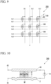
- FIG. 9 is a plan view of a magnetic memory 200 including a plurality of spin orbit torque type magnetoresistance effect elements 100 (see FIG. 8).
- FIG. 8 corresponds to a cross-sectional view of the spin orbit torque type magnetoresistance effect element 100 cut along the A-A plane in FIG. 9 .
- the spin orbit torque type magnetoresistance effect element 100 is arranged in a 3 ⁇ 3 matrix.
- FIG. 9 is an example of a magnetic memory, and the number and arrangement of the spin orbit torque type magnetoresistance effect elements 100 are arbitrary.
- One word line WL1 to WL3, one source line SL1 to SL3, and one read line RL1 to RL3 are each connected to the spin orbit torque type magnetoresistance effect element 100.
- a current is supplied to the spin orbit torque wiring 2 of an arbitrary spin orbit torque type magnetoresistance effect element 100 to perform a writing operation. Further, by selecting the read lines RL1 to RL3 and the source lines SL1 to SL3 to which current is applied, a current is caused to flow in the laminating direction of the functional section 60 of an arbitrary spin orbit torque type magnetoresistance effect element 100 to perform a reading operation.
- the word lines WL1 to WL3, the source lines SL1 to SL3, and the read lines RL1 to RL3 to which current is applied can be selected by transistors or the like. That is, since data of an arbitrary element can be read out from the plurality of spin orbit torque type magnetoresistance effect elements 100, the magnetic memory 200 can be utilized as a magnetic memory.
- FIG. 10 is a schematic cross-sectional view of a high-frequency magnetic element according to a fifth embodiment of the present invention.
- the high-frequency magnetic element 300 shown in FIG. 6 includes a spin orbit torque type magnetoresistance effect element 100 shown in FIG. 8 and a DC power supply 41 connected to the spin orbit torque type magnetoresistance effect element 100.
- a high-frequency current is input from the input terminal 42 of the high-frequency magnetic element 300.
- the high-frequency current generates a high-frequency magnetic field.
- a pure spin-current is induced and spin is injected into the first ferromagnetic layer 1.
- the magnetization M1 of the first ferromagnetic layer 1 vibrates due to the high-frequency magnetic field and the injected spin.
- the magnetization M1 of the first ferromagnetic layer 1 undergoes ferromagnetic resonance when the frequency of the high-frequency current input from the input terminal 42 is the ferromagnetic resonance frequency.
- the resistance value change of the functional section of the magnetoresistance effect becomes large. This change in resistance value is read out from the output terminal 43 by applying a direct current or a direct current voltage via the electrode 44 by the direct current power supply 41.
- the high-frequency magnetic element functions as a high-frequency filter.
Landscapes
- Engineering & Computer Science (AREA)
- Manufacturing & Machinery (AREA)
- Computer Hardware Design (AREA)
- Hall/Mr Elements (AREA)
- Mram Or Spin Memory Techniques (AREA)
Claims (8)
- Spinstrommagnetisierungsrotationselement (10), aufweisend:eine Spin-Orbit-Drehmoment-Verdrahtung (2), die sich in einer ersten Richtung erstreckt; undeine erste ferromagnetische Schicht (1), die in einer zweiten Richtung angeordnet ist, die die erste Richtung der Spin-Orbit-Drehmoment-Verdrahtung (2) schneidet,wobei die Spin-Orbit-Drehmoment-Verdrahtung (2) eine erste Oberfläche (2a), die auf der Seite angeordnet ist, auf der die erste ferromagnetische Schicht (1) angeordnet ist, und eine zweite Oberfläche (2b) gegenüber der ersten Oberfläche (2a) aufweist,die Spin-Orbit-Drehmoment-Verdrahtung (2) einen zweiten Bereich (2B) auf der ersten Oberfläche (2a) außerhalb eines ersten Bereichs (2A) aufweist, in dem die erste ferromagnetische Schicht (1) angeordnet ist, wobei der zweite Bereich (2B) einen vertieften Abschnitt bildet, der von dem ersten Bereich (2A) zu der Seite der zweiten Oberfläche (2b) vertieft ist, undder vertiefte Abschnitt in dem zweiten Bereich (2B) eine erste geneigte Oberfläche (2B1) aufweist, die in Bezug auf den ersten Bereich (2A) auf der ersten Oberfläche (2a) mit einem Neigungswinkel ϕ geneigt ist, der umso tiefer ist, je weiter er von dem ersten Bereich (2A) entfernt ist,dadurch gekennzeichnet, dass der vertiefte Abschnitt in dem zweiten Bereich (2B) weiterhin eine zweite geneigte Oberfläche (2B2) aufweist, die in Bezug auf den ersten Bereich (2A) auf der ersten Oberfläche (2a) so geneigt ist, dass sie umso tiefer ist, je näher sie sich an dem ersten Bereich befindet,und dass, wenn die Dicke der ersten ferromagnetischen Schicht (1) h ist und der kürzeste Abstand zwischen dem ersten Bereich (2A) und dem zweiten Bereich (2B) G ist, G>h/tan(10°+2ϕ) erfüllt ist.
- Spinstrommagnetisierungsrotationselement (10) nach Anspruch 1, wobei der Abstand G entlang der ersten Richtung verläuft.
- Spinstrommagnetisierungsrotationselement (10) nach Anspruch 1 oder 2, weiterhin aufweisend:eine Via-Verdrahtung (3), die sich in einer Richtung, die die erste Richtung schneidet, von der zweiten Oberfläche (2b) der Oberfläche der Spin-Orbit-Drehmoment-Verdrahtung (2) erstreckt,wobei der zweite Bereich (2B) die Via-Verdrahtung in einer Draufsicht aus der zweiten Richtung überlappt.
- Spinstrommagnetisierungsrotationselement (10) nach einem der Ansprüche 1 bis 3,
wobei die Tiefe des vertieften Abschnitts des zweiten Bereichs (2B) in Bezug auf den ersten Bereich (2A) geringer ist als die Dicke der Spin-Orbit-Drehmoment-Verdrahtung (2). - Spinstrommagnetisierungsrotationselement (10) nach einem der Ansprüche 1 bis 3,wobei die Tiefe des vertieften Abschnitts des zweiten Bereichs (2B) in Bezug auf den ersten Bereich (2A) gleich der Dicke der Spin-Orbit- Drehmoment-Verdrahtung (2) ist, undein vorstehender Abschnitt, der der Form des ausgesparten Abschnitts folgt, auf der Seite gegenüber der ersten Oberfläche (2a) ausgebildet ist.
- Spin-Orbit-Drehmoment-Typ-Magnetowiderstandseffektelement (100), aufweisend: das Spinstrommagnetisierungsrotationselement (10) nach einem der Ansprüche 1 bis 5;eine nichtmagnetische Schicht (5), die auf einer Oberfläche der Oberfläche der ersten ferromagnetischen Schicht (1) gegenüber einer Oberfläche angeordnet ist, die sich auf der Seite der Spin-Orbit-Drehmoment-Verdrahtung (2) befindet; undeine zweite ferromagnetische Schicht (6), die die nichtmagnetische Schicht sandwichartig zwischen der ersten ferromagnetischen Schicht (1) und der zweiten ferromagnetischen Schicht einschließt.
- Spin-Orbit-Drehmoment-Typ-Magnetowiderstandseffektelement (100) nach Anspruch 6,
wobei, wenn die Höhe eines Laminats (60), das die erste ferromagnetische Schicht (1), die nichtmagnetische Schicht (5) und die zweite ferromagnetische Schicht (6) enthält, H ist, G>H/tan(10°+2ϕ) erfüllt ist. - Verfahren zur Herstellung des Spinstrommagnetisierungsrotationselements (10) nach einem der Ansprüche 1 bis 5, dadurch gekennzeichnet, dass es die folgenden Verfahren umfasst:Herstellen eines Substrats mit einer Vielzahl von vertieften Abschnitten, die in einer Richtung auf einer Hauptoberfläche angeordnet sind, und Bilden einer Schicht, die durch ein Element für eine Spin-Orbit-Drehmoment-Verdrahtung (2) auf einer Hauptoberfläche des Substrats konfiguriert ist;Verarbeiten der Schicht des Elements für die Spin-Orbit-Drehmoment-Verdrahtung (2), so dass sie sich entlang der einen Richtung erstreckt, während sie die Vielzahl von vertieften Abschnitten bedeckt, um eine Spin-Orbit-Drehmoment-Verdrahtung (2) zu bilden;Bilden einer Schicht, die durch ein Element für eine erste ferromagnetische Schicht (1) auf der Spin-Orbit-Drehmoment-Verdrahtung (2) konfiguriert ist; undBilden einer ersten ferromagnetischen Schicht (1) durch Bearbeiten der Schicht des Elements für die erste ferromagnetische Schicht (1), so dass ein Abschnitt, der den vertieften Abschnitt überlappt, in Draufsicht aus der Laminierrichtung entfernt wird.
Applications Claiming Priority (2)
| Application Number | Priority Date | Filing Date | Title |
|---|---|---|---|
| JP2017172399 | 2017-09-07 | ||
| PCT/JP2018/029754 WO2019049591A1 (ja) | 2017-09-07 | 2018-08-08 | スピン流磁化反転素子及びスピン軌道トルク型磁気抵抗効果素子 |
Publications (3)
| Publication Number | Publication Date |
|---|---|
| EP3680938A1 EP3680938A1 (de) | 2020-07-15 |
| EP3680938A4 EP3680938A4 (de) | 2021-05-26 |
| EP3680938B1 true EP3680938B1 (de) | 2024-11-13 |
Family
ID=65633956
Family Applications (1)
| Application Number | Title | Priority Date | Filing Date |
|---|---|---|---|
| EP18854094.2A Active EP3680938B1 (de) | 2017-09-07 | 2018-08-08 | Spinstrom-magnetisierungsumkehrelement und magnetwiderstandseffektelement vom spin-orbit-drehmomenttyp |
Country Status (5)
| Country | Link |
|---|---|
| US (3) | US10910554B2 (de) |
| EP (1) | EP3680938B1 (de) |
| JP (1) | JP6642773B2 (de) |
| CN (1) | CN110268530B (de) |
| WO (1) | WO2019049591A1 (de) |
Families Citing this family (11)
| Publication number | Priority date | Publication date | Assignee | Title |
|---|---|---|---|---|
| JP6803575B2 (ja) * | 2016-06-24 | 2020-12-23 | 国立研究開発法人物質・材料研究機構 | I−iii−vi2化合物半導体を用いた磁気抵抗素子及びその製造方法、これを用いた磁気記憶装置並びにスピントランジスタ |
| JP6686990B2 (ja) * | 2017-09-04 | 2020-04-22 | Tdk株式会社 | スピン軌道トルク型磁化反転素子及び磁気メモリ |
| US10910554B2 (en) * | 2017-09-07 | 2021-02-02 | Tdk Corporation | Spin-current magnetization rotational element and spin orbit torque type magnetoresistance effect element |
| US11637234B2 (en) | 2017-09-15 | 2023-04-25 | Tokyo Institute Of Technology | Manufacturing method for multilayer structure of magnetic body and BiSb layer, magnetoresistive memory, and pure spin injection source |
| CN118201462A (zh) * | 2019-03-28 | 2024-06-14 | Tdk株式会社 | 存储元件、半导体装置、磁记录阵列和存储元件的制造方法 |
| CN114256408A (zh) * | 2020-09-24 | 2022-03-29 | 中芯国际集成电路制造(上海)有限公司 | 半导体结构及其形成方法 |
| US11373705B2 (en) * | 2020-11-23 | 2022-06-28 | Micron Technology, Inc. | Dynamically boosting read voltage for a memory device |
| US12020736B2 (en) | 2021-08-13 | 2024-06-25 | International Business Machines Corporation | Spin-orbit-torque magnetoresistive random-access memory array |
| US11793001B2 (en) | 2021-08-13 | 2023-10-17 | International Business Machines Corporation | Spin-orbit-torque magnetoresistive random-access memory |
| US11915734B2 (en) | 2021-08-13 | 2024-02-27 | International Business Machines Corporation | Spin-orbit-torque magnetoresistive random-access memory with integrated diode |
| US20250393480A1 (en) * | 2024-06-21 | 2025-12-25 | International Business Machines Corporation | Serpentine electrode for memory devices |
Family Cites Families (30)
| Publication number | Priority date | Publication date | Assignee | Title |
|---|---|---|---|---|
| JPS6164189A (ja) | 1984-09-06 | 1986-04-02 | 松下電器産業株式会社 | セラミツク多層配線基板の製造方法 |
| JP3153167B2 (ja) * | 1997-12-12 | 2001-04-03 | 日本電気株式会社 | 強磁性トンネル接合素子の製造方法 |
| JP2002314049A (ja) * | 2001-04-18 | 2002-10-25 | Nec Corp | 磁性メモリ及びその製造方法 |
| WO2003098637A1 (en) | 2002-05-22 | 2003-11-27 | Koninklijke Philips Electronics N.V. | Mram-cell and array-architecture with maximum read-out signal and reduced electromagnetic interference |
| US8379429B2 (en) | 2008-02-13 | 2013-02-19 | Nec Corporation | Domain wall motion element and magnetic random access memory |
| FR2963152B1 (fr) * | 2010-07-26 | 2013-03-29 | Centre Nat Rech Scient | Element de memoire magnetique |
| FR2963153B1 (fr) | 2010-07-26 | 2013-04-26 | Centre Nat Rech Scient | Element magnetique inscriptible |
| US8921959B2 (en) * | 2011-07-26 | 2014-12-30 | Taiwan Semiconductor Manufacturing Company, Ltd. | MRAM device and fabrication method thereof |
| US9105832B2 (en) | 2011-08-18 | 2015-08-11 | Cornell University | Spin hall effect magnetic apparatus, method and applications |
| JP2016021530A (ja) | 2014-07-15 | 2016-02-04 | ルネサスエレクトロニクス株式会社 | 半導体装置 |
| US9941468B2 (en) | 2014-08-08 | 2018-04-10 | Tohoku University | Magnetoresistance effect element and magnetic memory device |
| JP6200471B2 (ja) | 2015-09-14 | 2017-09-20 | 株式会社東芝 | 磁気メモリ |
| WO2017052494A1 (en) * | 2015-09-21 | 2017-03-30 | Intel Corporation | Flash anneal of a spin hall effect switched magnetic tunnel junction device to reduce resistivity of metal interconnects |
| US9608039B1 (en) * | 2015-11-16 | 2017-03-28 | Samsung Electronics Co., Ltd. | Magnetic junctions programmable using spin-orbit interaction torque in the absence of an external magnetic field |
| US10592802B2 (en) * | 2016-02-28 | 2020-03-17 | Purdue Research Foundation | Electronic synapse having spin-orbit torque induced spike-timing dependent plasticity |
| WO2017159432A1 (ja) * | 2016-03-14 | 2017-09-21 | Tdk株式会社 | 磁気メモリ |
| JP6674808B2 (ja) | 2016-03-22 | 2020-04-01 | Ntn株式会社 | 水力発電装置 |
| US10559747B1 (en) * | 2016-04-26 | 2020-02-11 | The Johns Hopkins University | Topological insulator-based high efficiency switching of magnetic unit, method and applications |
| JP2017216286A (ja) | 2016-05-30 | 2017-12-07 | 学校法人慶應義塾 | スピントロニクスデバイス及びこれを用いた記憶装置 |
| JP6374452B2 (ja) * | 2016-08-04 | 2018-08-15 | 株式会社東芝 | 磁気メモリ |
| JP6271654B1 (ja) * | 2016-08-05 | 2018-01-31 | 株式会社東芝 | 不揮発性メモリ |
| JP6926760B2 (ja) * | 2016-10-27 | 2021-08-25 | Tdk株式会社 | スピン軌道トルク型磁化反転素子、磁気メモリ及び高周波磁気デバイス |
| JP6972542B2 (ja) * | 2016-12-02 | 2021-11-24 | Tdk株式会社 | スピン流磁化反転素子、磁気抵抗効果素子および磁気メモリ |
| JP7003991B2 (ja) | 2017-04-14 | 2022-01-21 | Tdk株式会社 | 磁壁利用型アナログメモリ素子、磁壁利用型アナログメモリ、不揮発性ロジック回路及び磁気ニューロ素子 |
| JP6926666B2 (ja) * | 2017-05-18 | 2021-08-25 | Tdk株式会社 | スピン流磁化反転素子 |
| JP6495980B2 (ja) | 2017-08-08 | 2019-04-03 | 株式会社東芝 | 磁気メモリ |
| US10910554B2 (en) * | 2017-09-07 | 2021-02-02 | Tdk Corporation | Spin-current magnetization rotational element and spin orbit torque type magnetoresistance effect element |
| WO2019171715A1 (ja) | 2018-03-08 | 2019-09-12 | Tdk株式会社 | スピン素子及び磁気メモリ |
| US11575083B2 (en) * | 2018-04-02 | 2023-02-07 | Intel Corporation | Insertion layer between spin hall effect or spin orbit torque electrode and free magnet for improved magnetic memory |
| US12033062B2 (en) | 2018-11-21 | 2024-07-09 | Tdk Corporation | Reservoir element and neuromorphic element |
-
2018
- 2018-08-08 US US16/467,157 patent/US10910554B2/en active Active
- 2018-08-08 JP JP2019540677A patent/JP6642773B2/ja active Active
- 2018-08-08 WO PCT/JP2018/029754 patent/WO2019049591A1/ja not_active Ceased
- 2018-08-08 EP EP18854094.2A patent/EP3680938B1/de active Active
- 2018-08-08 CN CN201880008927.6A patent/CN110268530B/zh active Active
-
2020
- 2020-10-22 US US17/077,165 patent/US11641784B2/en active Active
-
2023
- 2023-02-24 US US18/113,747 patent/US12035639B2/en active Active
Also Published As
| Publication number | Publication date |
|---|---|
| US11641784B2 (en) | 2023-05-02 |
| WO2019049591A1 (ja) | 2019-03-14 |
| EP3680938A1 (de) | 2020-07-15 |
| CN110268530B (zh) | 2022-07-26 |
| US20190319183A1 (en) | 2019-10-17 |
| EP3680938A4 (de) | 2021-05-26 |
| US12035639B2 (en) | 2024-07-09 |
| US10910554B2 (en) | 2021-02-02 |
| JPWO2019049591A1 (ja) | 2019-12-19 |
| US20230200259A1 (en) | 2023-06-22 |
| US20210043831A1 (en) | 2021-02-11 |
| JP6642773B2 (ja) | 2020-02-12 |
| CN110268530A (zh) | 2019-09-20 |
Similar Documents
| Publication | Publication Date | Title |
|---|---|---|
| US12035639B2 (en) | Spin-current magnetization rotational element and spin orbit torque type magnetoresistance effect element | |
| US10665375B2 (en) | Spin current magnetization rotational element, spin-orbit-torque magnetoresistance effect element, magnetic memory, and high-frequency magnetic element | |
| CN109786544B (zh) | 自旋轨道转矩型磁化旋转元件、磁阻效应元件和磁存储器 | |
| CN109427965B (zh) | 自旋流磁化旋转元件、自旋轨道转矩型磁阻效应元件 | |
| US10923649B2 (en) | Spin current magnetization rotation magnetoresistance effect element, and magnetic memory | |
| CN110914974B (zh) | 自旋轨道转矩型磁化旋转元件、自旋轨道转矩型磁阻效应元件和磁存储器 | |
| US11211547B2 (en) | Spin-orbit-torque type magnetization rotating element, spin-orbit-torque type magnetoresistance effect element, and magnetic memory | |
| US10998493B2 (en) | Spin-orbit-torque magnetoresistance effect element and magnetic memory | |
| JP6428988B1 (ja) | スピン素子の安定化方法及びスピン素子の製造方法 | |
| CN108011038A (zh) | 自旋轨道转矩型磁阻效应元件及其制造方法 | |
| CN111129285A (zh) | 自旋轨道转矩型磁化旋转元件、自旋轨道转矩型磁阻效应元件和磁存储器 | |
| JP6462191B1 (ja) | データの書き込み方法、検査方法、スピン素子の製造方法及び磁気抵抗効果素子 | |
| JP7139701B2 (ja) | スピン流磁化反転素子、スピン軌道トルク型磁気抵抗効果素子、磁気メモリ及び高周波磁気素子 | |
| WO2019167197A1 (ja) | スピン素子の安定化方法及びスピン素子の製造方法 | |
| CN111480240A (zh) | 自旋轨道转矩型磁阻效应元件和磁存储器 | |
| CN113330582A (zh) | 自旋轨道转矩型磁化旋转元件、自旋轨道转矩型磁阻效应元件、磁存储器及储备池元件 | |
| US20200083430A1 (en) | Spin-orbit-torque magnetization rotational element and spin-orbit-torque magnetoresistance effect element | |
| JP2020035792A (ja) | スピン軌道トルク型磁化回転素子、スピン軌道トルク型磁気抵抗効果素子及び磁気メモリ | |
| JP7124788B2 (ja) | スピン流磁化回転型磁気抵抗効果素子、及び磁気メモリ | |
| CN115000291B (zh) | 磁器件 | |
| US11925123B2 (en) | Spin-orbit torque type magnetization rotational element, spin-orbit torque type magnetoresistance effect element, and magnetic memory | |
| US11264071B2 (en) | Magnetoresistance effect element and magnetic memory | |
| WO2022190346A1 (ja) | 磁気抵抗効果素子及び磁気メモリ |
Legal Events
| Date | Code | Title | Description |
|---|---|---|---|
| STAA | Information on the status of an ep patent application or granted ep patent |
Free format text: STATUS: THE INTERNATIONAL PUBLICATION HAS BEEN MADE |
|
| PUAI | Public reference made under article 153(3) epc to a published international application that has entered the european phase |
Free format text: ORIGINAL CODE: 0009012 |
|
| STAA | Information on the status of an ep patent application or granted ep patent |
Free format text: STATUS: REQUEST FOR EXAMINATION WAS MADE |
|
| 17P | Request for examination filed |
Effective date: 20190606 |
|
| AK | Designated contracting states |
Kind code of ref document: A1 Designated state(s): AL AT BE BG CH CY CZ DE DK EE ES FI FR GB GR HR HU IE IS IT LI LT LU LV MC MK MT NL NO PL PT RO RS SE SI SK SM TR |
|
| AX | Request for extension of the european patent |
Extension state: BA ME |
|
| DAV | Request for validation of the european patent (deleted) | ||
| DAX | Request for extension of the european patent (deleted) | ||
| A4 | Supplementary search report drawn up and despatched |
Effective date: 20210422 |
|
| RIC1 | Information provided on ipc code assigned before grant |
Ipc: H01L 29/82 20060101AFI20210416BHEP Ipc: H01L 21/8239 20060101ALI20210416BHEP Ipc: H01L 27/105 20060101ALI20210416BHEP Ipc: H01L 43/08 20060101ALI20210416BHEP Ipc: H01L 43/12 20060101ALI20210416BHEP Ipc: H03B 15/00 20060101ALI20210416BHEP Ipc: G11C 11/16 20060101ALI20210416BHEP Ipc: H01L 43/02 20060101ALI20210416BHEP |
|
| STAA | Information on the status of an ep patent application or granted ep patent |
Free format text: STATUS: EXAMINATION IS IN PROGRESS |
|
| 17Q | First examination report despatched |
Effective date: 20230310 |
|
| REG | Reference to a national code |
Ref country code: DE Ref legal event code: R079 Ref document number: 602018076597 Country of ref document: DE Free format text: PREVIOUS MAIN CLASS: H01L0029820000 Ipc: H10N0050100000 |
|
| GRAP | Despatch of communication of intention to grant a patent |
Free format text: ORIGINAL CODE: EPIDOSNIGR1 |
|
| STAA | Information on the status of an ep patent application or granted ep patent |
Free format text: STATUS: GRANT OF PATENT IS INTENDED |
|
| RIC1 | Information provided on ipc code assigned before grant |
Ipc: H03B 15/00 20060101ALI20240628BHEP Ipc: H01L 29/82 20060101ALI20240628BHEP Ipc: G11C 11/16 20060101ALI20240628BHEP Ipc: H10N 50/80 20230101ALI20240628BHEP Ipc: H10N 50/10 20230101AFI20240628BHEP |
|
| INTG | Intention to grant announced |
Effective date: 20240806 |
|
| GRAS | Grant fee paid |
Free format text: ORIGINAL CODE: EPIDOSNIGR3 |
|
| GRAA | (expected) grant |
Free format text: ORIGINAL CODE: 0009210 |
|
| STAA | Information on the status of an ep patent application or granted ep patent |
Free format text: STATUS: THE PATENT HAS BEEN GRANTED |
|
| AK | Designated contracting states |
Kind code of ref document: B1 Designated state(s): AL AT BE BG CH CY CZ DE DK EE ES FI FR GB GR HR HU IE IS IT LI LT LU LV MC MK MT NL NO PL PT RO RS SE SI SK SM TR |
|
| P01 | Opt-out of the competence of the unified patent court (upc) registered |
Free format text: CASE NUMBER: APP_53386/2024 Effective date: 20240925 |
|
| REG | Reference to a national code |
Ref country code: GB Ref legal event code: FG4D |
|
| REG | Reference to a national code |
Ref country code: CH Ref legal event code: EP |
|
| REG | Reference to a national code |
Ref country code: IE Ref legal event code: FG4D |
|
| REG | Reference to a national code |
Ref country code: DE Ref legal event code: R096 Ref document number: 602018076597 Country of ref document: DE |
|
| REG | Reference to a national code |
Ref country code: LT Ref legal event code: MG9D |
|
| REG | Reference to a national code |
Ref country code: NL Ref legal event code: MP Effective date: 20241113 |
|
| PG25 | Lapsed in a contracting state [announced via postgrant information from national office to epo] |
Ref country code: HR Free format text: LAPSE BECAUSE OF FAILURE TO SUBMIT A TRANSLATION OF THE DESCRIPTION OR TO PAY THE FEE WITHIN THE PRESCRIBED TIME-LIMIT Effective date: 20241113 Ref country code: IS Free format text: LAPSE BECAUSE OF FAILURE TO SUBMIT A TRANSLATION OF THE DESCRIPTION OR TO PAY THE FEE WITHIN THE PRESCRIBED TIME-LIMIT Effective date: 20250313 Ref country code: PT Free format text: LAPSE BECAUSE OF FAILURE TO SUBMIT A TRANSLATION OF THE DESCRIPTION OR TO PAY THE FEE WITHIN THE PRESCRIBED TIME-LIMIT Effective date: 20250313 |
|
| PG25 | Lapsed in a contracting state [announced via postgrant information from national office to epo] |
Ref country code: FI Free format text: LAPSE BECAUSE OF FAILURE TO SUBMIT A TRANSLATION OF THE DESCRIPTION OR TO PAY THE FEE WITHIN THE PRESCRIBED TIME-LIMIT Effective date: 20241113 Ref country code: NL Free format text: LAPSE BECAUSE OF FAILURE TO SUBMIT A TRANSLATION OF THE DESCRIPTION OR TO PAY THE FEE WITHIN THE PRESCRIBED TIME-LIMIT Effective date: 20241113 |
|
| REG | Reference to a national code |
Ref country code: AT Ref legal event code: MK05 Ref document number: 1742653 Country of ref document: AT Kind code of ref document: T Effective date: 20241113 |
|
| PG25 | Lapsed in a contracting state [announced via postgrant information from national office to epo] |
Ref country code: BG Free format text: LAPSE BECAUSE OF FAILURE TO SUBMIT A TRANSLATION OF THE DESCRIPTION OR TO PAY THE FEE WITHIN THE PRESCRIBED TIME-LIMIT Effective date: 20241113 |
|
| PG25 | Lapsed in a contracting state [announced via postgrant information from national office to epo] |
Ref country code: ES Free format text: LAPSE BECAUSE OF FAILURE TO SUBMIT A TRANSLATION OF THE DESCRIPTION OR TO PAY THE FEE WITHIN THE PRESCRIBED TIME-LIMIT Effective date: 20241113 |
|
| PG25 | Lapsed in a contracting state [announced via postgrant information from national office to epo] |
Ref country code: NO Free format text: LAPSE BECAUSE OF FAILURE TO SUBMIT A TRANSLATION OF THE DESCRIPTION OR TO PAY THE FEE WITHIN THE PRESCRIBED TIME-LIMIT Effective date: 20250213 |
|
| PG25 | Lapsed in a contracting state [announced via postgrant information from national office to epo] |
Ref country code: LV Free format text: LAPSE BECAUSE OF FAILURE TO SUBMIT A TRANSLATION OF THE DESCRIPTION OR TO PAY THE FEE WITHIN THE PRESCRIBED TIME-LIMIT Effective date: 20241113 Ref country code: AT Free format text: LAPSE BECAUSE OF FAILURE TO SUBMIT A TRANSLATION OF THE DESCRIPTION OR TO PAY THE FEE WITHIN THE PRESCRIBED TIME-LIMIT Effective date: 20241113 Ref country code: GR Free format text: LAPSE BECAUSE OF FAILURE TO SUBMIT A TRANSLATION OF THE DESCRIPTION OR TO PAY THE FEE WITHIN THE PRESCRIBED TIME-LIMIT Effective date: 20250214 |
|
| PG25 | Lapsed in a contracting state [announced via postgrant information from national office to epo] |
Ref country code: PL Free format text: LAPSE BECAUSE OF FAILURE TO SUBMIT A TRANSLATION OF THE DESCRIPTION OR TO PAY THE FEE WITHIN THE PRESCRIBED TIME-LIMIT Effective date: 20241113 |
|
| PG25 | Lapsed in a contracting state [announced via postgrant information from national office to epo] |
Ref country code: RS Free format text: LAPSE BECAUSE OF FAILURE TO SUBMIT A TRANSLATION OF THE DESCRIPTION OR TO PAY THE FEE WITHIN THE PRESCRIBED TIME-LIMIT Effective date: 20250213 |
|
| PG25 | Lapsed in a contracting state [announced via postgrant information from national office to epo] |
Ref country code: SM Free format text: LAPSE BECAUSE OF FAILURE TO SUBMIT A TRANSLATION OF THE DESCRIPTION OR TO PAY THE FEE WITHIN THE PRESCRIBED TIME-LIMIT Effective date: 20241113 |
|
| PG25 | Lapsed in a contracting state [announced via postgrant information from national office to epo] |
Ref country code: DK Free format text: LAPSE BECAUSE OF FAILURE TO SUBMIT A TRANSLATION OF THE DESCRIPTION OR TO PAY THE FEE WITHIN THE PRESCRIBED TIME-LIMIT Effective date: 20241113 |
|
| PG25 | Lapsed in a contracting state [announced via postgrant information from national office to epo] |
Ref country code: EE Free format text: LAPSE BECAUSE OF FAILURE TO SUBMIT A TRANSLATION OF THE DESCRIPTION OR TO PAY THE FEE WITHIN THE PRESCRIBED TIME-LIMIT Effective date: 20241113 |
|
| PG25 | Lapsed in a contracting state [announced via postgrant information from national office to epo] |
Ref country code: RO Free format text: LAPSE BECAUSE OF FAILURE TO SUBMIT A TRANSLATION OF THE DESCRIPTION OR TO PAY THE FEE WITHIN THE PRESCRIBED TIME-LIMIT Effective date: 20241113 |
|
| PG25 | Lapsed in a contracting state [announced via postgrant information from national office to epo] |
Ref country code: SK Free format text: LAPSE BECAUSE OF FAILURE TO SUBMIT A TRANSLATION OF THE DESCRIPTION OR TO PAY THE FEE WITHIN THE PRESCRIBED TIME-LIMIT Effective date: 20241113 |
|
| PG25 | Lapsed in a contracting state [announced via postgrant information from national office to epo] |
Ref country code: CZ Free format text: LAPSE BECAUSE OF FAILURE TO SUBMIT A TRANSLATION OF THE DESCRIPTION OR TO PAY THE FEE WITHIN THE PRESCRIBED TIME-LIMIT Effective date: 20241113 |
|
| PG25 | Lapsed in a contracting state [announced via postgrant information from national office to epo] |
Ref country code: IT Free format text: LAPSE BECAUSE OF FAILURE TO SUBMIT A TRANSLATION OF THE DESCRIPTION OR TO PAY THE FEE WITHIN THE PRESCRIBED TIME-LIMIT Effective date: 20241113 |
|
| REG | Reference to a national code |
Ref country code: DE Ref legal event code: R097 Ref document number: 602018076597 Country of ref document: DE |
|
| PG25 | Lapsed in a contracting state [announced via postgrant information from national office to epo] |
Ref country code: SE Free format text: LAPSE BECAUSE OF FAILURE TO SUBMIT A TRANSLATION OF THE DESCRIPTION OR TO PAY THE FEE WITHIN THE PRESCRIBED TIME-LIMIT Effective date: 20241113 |
|
| PLBE | No opposition filed within time limit |
Free format text: ORIGINAL CODE: 0009261 |
|
| STAA | Information on the status of an ep patent application or granted ep patent |
Free format text: STATUS: NO OPPOSITION FILED WITHIN TIME LIMIT |
|
| PGFP | Annual fee paid to national office [announced via postgrant information from national office to epo] |
Ref country code: DE Payment date: 20250821 Year of fee payment: 8 |
|
| PGFP | Annual fee paid to national office [announced via postgrant information from national office to epo] |
Ref country code: FR Payment date: 20250827 Year of fee payment: 8 |
|
| 26N | No opposition filed |
Effective date: 20250814 |
|
| REG | Reference to a national code |
Ref country code: CH Ref legal event code: H13 Free format text: ST27 STATUS EVENT CODE: U-0-0-H10-H13 (AS PROVIDED BY THE NATIONAL OFFICE) Effective date: 20260324 |