EP3671331A1 - Arraysubstrat und verfahren zur herstellung davon sowie anzeigetafel - Google Patents
Arraysubstrat und verfahren zur herstellung davon sowie anzeigetafel Download PDFInfo
- Publication number
- EP3671331A1 EP3671331A1 EP18846203.0A EP18846203A EP3671331A1 EP 3671331 A1 EP3671331 A1 EP 3671331A1 EP 18846203 A EP18846203 A EP 18846203A EP 3671331 A1 EP3671331 A1 EP 3671331A1
- Authority
- EP
- European Patent Office
- Prior art keywords
- transparent substrate
- light reflecting
- array substrate
- coarse region
- present disclosure
- Prior art date
- Legal status (The legal status is an assumption and is not a legal conclusion. Google has not performed a legal analysis and makes no representation as to the accuracy of the status listed.)
- Withdrawn
Links
- 239000000758 substrate Substances 0.000 title claims abstract description 120
- 238000000034 method Methods 0.000 title claims abstract description 19
- 238000004519 manufacturing process Methods 0.000 title claims abstract description 11
- 239000011241 protective layer Substances 0.000 claims description 26
- 239000000463 material Substances 0.000 claims description 18
- KRHYYFGTRYWZRS-UHFFFAOYSA-N Fluorane Chemical compound F KRHYYFGTRYWZRS-UHFFFAOYSA-N 0.000 claims description 8
- VEXZGXHMUGYJMC-UHFFFAOYSA-N Hydrochloric acid Chemical compound Cl VEXZGXHMUGYJMC-UHFFFAOYSA-N 0.000 claims description 8
- 239000011159 matrix material Substances 0.000 claims description 8
- 238000001312 dry etching Methods 0.000 claims description 7
- 239000011521 glass Substances 0.000 claims description 6
- 238000001039 wet etching Methods 0.000 claims description 6
- 229920002120 photoresistant polymer Polymers 0.000 claims description 5
- 238000000059 patterning Methods 0.000 claims description 4
- 239000000843 powder Substances 0.000 claims description 4
- 239000010410 layer Substances 0.000 description 10
- 230000000694 effects Effects 0.000 description 8
- 230000015572 biosynthetic process Effects 0.000 description 7
- 238000010586 diagram Methods 0.000 description 2
- 239000002184 metal Substances 0.000 description 2
- 239000007769 metal material Substances 0.000 description 2
- 230000003287 optical effect Effects 0.000 description 2
- 238000002161 passivation Methods 0.000 description 2
- 230000003044 adaptive effect Effects 0.000 description 1
- 238000010276 construction Methods 0.000 description 1
- 238000005516 engineering process Methods 0.000 description 1
- 230000014509 gene expression Effects 0.000 description 1
- 238000012986 modification Methods 0.000 description 1
- 230000004048 modification Effects 0.000 description 1
- 230000005855 radiation Effects 0.000 description 1
- 230000003313 weakening effect Effects 0.000 description 1
Images


Classifications
-
- G—PHYSICS
- G02—OPTICS
- G02F—OPTICAL DEVICES OR ARRANGEMENTS FOR THE CONTROL OF LIGHT BY MODIFICATION OF THE OPTICAL PROPERTIES OF THE MEDIA OF THE ELEMENTS INVOLVED THEREIN; NON-LINEAR OPTICS; FREQUENCY-CHANGING OF LIGHT; OPTICAL LOGIC ELEMENTS; OPTICAL ANALOGUE/DIGITAL CONVERTERS
- G02F1/00—Devices or arrangements for the control of the intensity, colour, phase, polarisation or direction of light arriving from an independent light source, e.g. switching, gating or modulating; Non-linear optics
- G02F1/01—Devices or arrangements for the control of the intensity, colour, phase, polarisation or direction of light arriving from an independent light source, e.g. switching, gating or modulating; Non-linear optics for the control of the intensity, phase, polarisation or colour
- G02F1/13—Devices or arrangements for the control of the intensity, colour, phase, polarisation or direction of light arriving from an independent light source, e.g. switching, gating or modulating; Non-linear optics for the control of the intensity, phase, polarisation or colour based on liquid crystals, e.g. single liquid crystal display cells
- G02F1/133—Constructional arrangements; Operation of liquid crystal cells; Circuit arrangements
- G02F1/1333—Constructional arrangements; Manufacturing methods
- G02F1/1335—Structural association of cells with optical devices, e.g. polarisers or reflectors
- G02F1/133553—Reflecting elements
-
- G—PHYSICS
- G02—OPTICS
- G02F—OPTICAL DEVICES OR ARRANGEMENTS FOR THE CONTROL OF LIGHT BY MODIFICATION OF THE OPTICAL PROPERTIES OF THE MEDIA OF THE ELEMENTS INVOLVED THEREIN; NON-LINEAR OPTICS; FREQUENCY-CHANGING OF LIGHT; OPTICAL LOGIC ELEMENTS; OPTICAL ANALOGUE/DIGITAL CONVERTERS
- G02F1/00—Devices or arrangements for the control of the intensity, colour, phase, polarisation or direction of light arriving from an independent light source, e.g. switching, gating or modulating; Non-linear optics
- G02F1/01—Devices or arrangements for the control of the intensity, colour, phase, polarisation or direction of light arriving from an independent light source, e.g. switching, gating or modulating; Non-linear optics for the control of the intensity, phase, polarisation or colour
- G02F1/13—Devices or arrangements for the control of the intensity, colour, phase, polarisation or direction of light arriving from an independent light source, e.g. switching, gating or modulating; Non-linear optics for the control of the intensity, phase, polarisation or colour based on liquid crystals, e.g. single liquid crystal display cells
- G02F1/133—Constructional arrangements; Operation of liquid crystal cells; Circuit arrangements
- G02F1/136—Liquid crystal cells structurally associated with a semi-conducting layer or substrate, e.g. cells forming part of an integrated circuit
- G02F1/1362—Active matrix addressed cells
- G02F1/136209—Light shielding layers, e.g. black matrix, incorporated in the active matrix substrate, e.g. structurally associated with the switching element
-
- H—ELECTRICITY
- H10—SEMICONDUCTOR DEVICES; ELECTRIC SOLID-STATE DEVICES NOT OTHERWISE PROVIDED FOR
- H10D—INORGANIC ELECTRIC SEMICONDUCTOR DEVICES
- H10D86/00—Integrated devices formed in or on insulating or conducting substrates, e.g. formed in silicon-on-insulator [SOI] substrates or on stainless steel or glass substrates
- H10D86/01—Manufacture or treatment
- H10D86/021—Manufacture or treatment of multiple TFTs
- H10D86/0212—Manufacture or treatment of multiple TFTs comprising manufacture, treatment or coating of substrates
-
- H—ELECTRICITY
- H10—SEMICONDUCTOR DEVICES; ELECTRIC SOLID-STATE DEVICES NOT OTHERWISE PROVIDED FOR
- H10D—INORGANIC ELECTRIC SEMICONDUCTOR DEVICES
- H10D86/00—Integrated devices formed in or on insulating or conducting substrates, e.g. formed in silicon-on-insulator [SOI] substrates or on stainless steel or glass substrates
- H10D86/40—Integrated devices formed in or on insulating or conducting substrates, e.g. formed in silicon-on-insulator [SOI] substrates or on stainless steel or glass substrates characterised by multiple TFTs
- H10D86/411—Integrated devices formed in or on insulating or conducting substrates, e.g. formed in silicon-on-insulator [SOI] substrates or on stainless steel or glass substrates characterised by multiple TFTs characterised by materials, geometry or structure of the substrates
-
- H—ELECTRICITY
- H10—SEMICONDUCTOR DEVICES; ELECTRIC SOLID-STATE DEVICES NOT OTHERWISE PROVIDED FOR
- H10D—INORGANIC ELECTRIC SEMICONDUCTOR DEVICES
- H10D86/00—Integrated devices formed in or on insulating or conducting substrates, e.g. formed in silicon-on-insulator [SOI] substrates or on stainless steel or glass substrates
- H10D86/40—Integrated devices formed in or on insulating or conducting substrates, e.g. formed in silicon-on-insulator [SOI] substrates or on stainless steel or glass substrates characterised by multiple TFTs
- H10D86/60—Integrated devices formed in or on insulating or conducting substrates, e.g. formed in silicon-on-insulator [SOI] substrates or on stainless steel or glass substrates characterised by multiple TFTs wherein the TFTs are in active matrices
-
- G—PHYSICS
- G02—OPTICS
- G02F—OPTICAL DEVICES OR ARRANGEMENTS FOR THE CONTROL OF LIGHT BY MODIFICATION OF THE OPTICAL PROPERTIES OF THE MEDIA OF THE ELEMENTS INVOLVED THEREIN; NON-LINEAR OPTICS; FREQUENCY-CHANGING OF LIGHT; OPTICAL LOGIC ELEMENTS; OPTICAL ANALOGUE/DIGITAL CONVERTERS
- G02F1/00—Devices or arrangements for the control of the intensity, colour, phase, polarisation or direction of light arriving from an independent light source, e.g. switching, gating or modulating; Non-linear optics
- G02F1/01—Devices or arrangements for the control of the intensity, colour, phase, polarisation or direction of light arriving from an independent light source, e.g. switching, gating or modulating; Non-linear optics for the control of the intensity, phase, polarisation or colour
- G02F1/13—Devices or arrangements for the control of the intensity, colour, phase, polarisation or direction of light arriving from an independent light source, e.g. switching, gating or modulating; Non-linear optics for the control of the intensity, phase, polarisation or colour based on liquid crystals, e.g. single liquid crystal display cells
- G02F1/133—Constructional arrangements; Operation of liquid crystal cells; Circuit arrangements
- G02F1/1333—Constructional arrangements; Manufacturing methods
- G02F1/1335—Structural association of cells with optical devices, e.g. polarisers or reflectors
- G02F1/13356—Structural association of cells with optical devices, e.g. polarisers or reflectors characterised by the placement of the optical elements
- G02F1/133565—Structural association of cells with optical devices, e.g. polarisers or reflectors characterised by the placement of the optical elements inside the LC elements, i.e. between the cell substrates
-
- G—PHYSICS
- G02—OPTICS
- G02F—OPTICAL DEVICES OR ARRANGEMENTS FOR THE CONTROL OF LIGHT BY MODIFICATION OF THE OPTICAL PROPERTIES OF THE MEDIA OF THE ELEMENTS INVOLVED THEREIN; NON-LINEAR OPTICS; FREQUENCY-CHANGING OF LIGHT; OPTICAL LOGIC ELEMENTS; OPTICAL ANALOGUE/DIGITAL CONVERTERS
- G02F2203/00—Function characteristic
- G02F2203/02—Function characteristic reflective
-
- G—PHYSICS
- G02—OPTICS
- G02F—OPTICAL DEVICES OR ARRANGEMENTS FOR THE CONTROL OF LIGHT BY MODIFICATION OF THE OPTICAL PROPERTIES OF THE MEDIA OF THE ELEMENTS INVOLVED THEREIN; NON-LINEAR OPTICS; FREQUENCY-CHANGING OF LIGHT; OPTICAL LOGIC ELEMENTS; OPTICAL ANALOGUE/DIGITAL CONVERTERS
- G02F2203/00—Function characteristic
- G02F2203/03—Function characteristic scattering
-
- H—ELECTRICITY
- H10—SEMICONDUCTOR DEVICES; ELECTRIC SOLID-STATE DEVICES NOT OTHERWISE PROVIDED FOR
- H10D—INORGANIC ELECTRIC SEMICONDUCTOR DEVICES
- H10D86/00—Integrated devices formed in or on insulating or conducting substrates, e.g. formed in silicon-on-insulator [SOI] substrates or on stainless steel or glass substrates
- H10D86/40—Integrated devices formed in or on insulating or conducting substrates, e.g. formed in silicon-on-insulator [SOI] substrates or on stainless steel or glass substrates characterised by multiple TFTs
- H10D86/441—Interconnections, e.g. scanning lines
Definitions
- the present disclosure relate to the field of display technologies, and in particular, to an array substrate, a method for manufacturing the same and a display panel thereof.
- Embodiments of the present disclosure provide an array substrate, a method for manufacturing the same, and a display panel thereof.
- an array substrate includes: a transparent substrate having a first side surface and a second side surface opposite to the first side surface; and a light reflecting structure disposed on the first side surface of the transparent substrate, wherein the second side surface of the transparent substrate has a coarse region, an orthographic projection of the coarse region on the transparent substrate coinciding with an orthographic projection of the light reflecting structure on the transparent substrate.
- the coarse region is a portion of a base material of the transparent substrate.
- the light reflecting structure includes a black matrix and a conductive structure.
- the conductive structure includes at least one of a data line, a data lead, a gate line, and a gate lead formed on the transparent substrate.
- the base material of the transparent substrate is glass.
- a display panel including the array substrate described in the first aspect of the embodiment of the present disclosure.
- a method for manufacturing an array substrate includes: providing a transparent substrate having a first side surface and a second side surface opposite to the first side surface, a light reflecting structure being disposed on the first side surface of the transparent substrate; and coarsening the second side surface of the transparent substrate to form a coarse region, wherein an orthographic projection of the coarse region on the transparent substrate coincides with an orthographic projection of the light reflecting structure on the transparent substrate.
- the coarse region is a portion of a base material of the transparent substrate.
- the coarsening includes: forming a protective layer on the second side surface of the transparent substrate; patterning the protective layer to form a patterned protective layer, wherein the patterned protective layer has an opening, an orthographic projection of the opening on the transparent substrate coinciding with an orthographic projection of the light reflecting structure on the transparent substrate; coarsening a portion, exposed by the opening, of the second side surface of the transparent substrate to form the coarse region; and removing the patterned protective layer.
- a material of the protective layer is a negative photoresist
- the patterning includes exposing the negative photoresist using the light reflecting structure as a mask.
- coarsening the portion, exposed by the opening, of the second side surface of the transparent substrate to form the coarse region includes a wet or dry etching.
- the base material of the transparent substrate is glass.
- the wet etching employs an etchant including frost powder, hydrofluoric acid, and hydrochloric acid.
- the dry etching employs a plasma of at least one of He, CF 4 , H 2 , and O 2 .
- the light reflecting structure includes a black matrix and a conductive structure.
- the conductive structure includes at least one of a data line, a data lead, a gate line, and a gate lead formed on the transparent substrate.
- FIG. 1 shows a display panel without a frame.
- a backlight module and an array substrate are respectively disposed on opposite sides of a color filter substrate.
- the array substrate is disposed on a display side.
- an array substrate is provided.
- a surface of a transparent substrate of the array substrate has a coarse region, which can reduce the reflection of ambient light caused by an undesired reflective structure (for example, a black matrix and a conductive structure) located on the transparent substrate, thereby improving the display effect of the display device.
- an undesired reflective structure for example, a black matrix and a conductive structure
- FIG. 2 is a schematic view showing a cross section of an array substrate according to an embodiment of the present disclosure.
- an array substrate 10 includes: a transparent substrate 1 having a first side surface 11 and a second side surface 12 opposite to the first side surface 11; and a plurality of light reflecting structures 2 located on the first side surface 11 of the transparent substrate 1.
- the second side surface 12 of the transparent substrate 1 has a plurality of coarse regions 13, an orthographic projection of the coarse region 13 on the transparent substrate 1 coinciding with an orthographic projection of the light reflecting structure 2 on the transparent substrate 1.
- the coarse region 13 is a portion of a surface of a base material of the transparent substrate 1.
- the base material of the transparent substrate 1 may be glass.
- the light reflecting structure 2 may include a black matrix and a conductive structure.
- the conductive structure may include at least one of a data line, a data lead, a gate line, and a gate lead formed on the transparent substrate 1.
- the light reflecting structure 2 may be made of a metal material.
- the light incident on the coarse region 13 is diffusely reflected due to the transparent substrate 1 has the coarse region 13, thereby weakening the reflection of ambient light along a certain direction on the light reflecting structure 2 and thus improving the display effect of the display device.
- FIG. 3 is a schematic structural view showing a display panel according to an embodiment of the present disclosure.
- the display panel 100 includes the array substrate 10 as shown in FIG. 1 , so that the display effect of the display panel 100 can be improved.
- a method for manufacturing an array substrate is provided. It is possible to manufacture an array substrate having a coarse region on a surface of a base material of a transparent substrate, thereby improving the display effect of the display device.
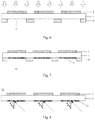
- FIG. 4 is a flow chart schematically showing a method for manufacturing an array substrate according to an embodiment of the present disclosure.
- a transparent substrate is provided; and in step S402, a protective layer is formed on a surface of the transparent substrate.
- FIG. 5 is a schematic view showing a cross section of formation of a protective layer according to an embodiment of the present disclosure.
- a transparent substrate 1 having a first side surface 11 and a second side surface 12 opposite to the first side surface 11 is provided, and a plurality of light reflecting structures 2 are disposed on the first side surface 11 of the transparent substrate 1.
- a protective layer 4 is formed on the second side surface 12 of the transparent substrate 1.
- FIG. 6 is a schematic view showing a cross section of formation of a patterned protective layer according to an embodiment of the present disclosure.
- the protective layer 4 is patterned to form a patterned protective layer 41.
- the protective layer 4 is exposed to radiation such as ultraviolet rays by using the light reflecting structure 2 as a mask.
- a material of the protective layer 4 is a negative photoresist.
- the patterned protective layer 41 has a plurality of openings 42, an orthographic projection of the opening 42 on the transparent substrate 1 coinciding with an orthographic projection of the light reflecting structure 2 on the transparent substrate 1.
- the light reflecting structure 2 may include a black matrix and a conductive structure.
- the conductive structure may include at least one of a data line, a data lead, a gate line, and a gate lead formed on the transparent substrate 1.
- the light reflecting structure 2 may be made of a metal material.
- FIG. 7 is a schematic view showing a cross section of formation of a coarse region according to an embodiment of the present disclosure.
- the second side surface 12 of the transparent substrate 1 is coarsened to form the coarse region 13.
- a portion, exposed by the opening 42, of the second side surface 12 of the transparent substrate 1 is coarsened to form the coarse region 13.
- the coarse region 13 is a portion of a surface of a base material of the transparent substrate 1.
- the base material of the transparent substrate 1 is glass.
- the above coarsening may include a wet or dry etching.
- the wet etching employs an etchant including frost powder, hydrofluoric acid, and hydrochloric acid.
- an etchant including frost powder, hydrofluoric acid, and hydrochloric acid.
- the frost powder, hydrofluoric acid, and hydrochloric acid are mixed to prepare an etchant, and the etchant is then applied (for example, sprayed) to at least a portion, exposed by the opening 42, of the second side surface 12 of the transparent substrate 1, the portion being sufficiently reacted with the etchant to form the coarse region 13.
- the dry etching employs a plasma of at least one of He, CF 4 , H 2 , and O 2 .
- a portion, exposed by the opening 42, of the second side surface 12 of the transparent substrate 1 is physically bombarded with a plasma of at least one of He, CF 4 , H 2 , and O 2 within a dry etching apparatus, thereby forming the coarse region 13.
- step S405 the patterned protective layer is removed. Specifically, the patterned protective layer 41 is removed, thereby manufacturing the array substrate 10 as shown in FIG. 2 .
- FIG. 8 is a view schematically showing a optical path of a reflected light when ambient light is incident on an array substrate according to an embodiment of the present disclosure.
- the light incident on the coarse region 13 is diffusely reflected so that ambient light is reflected in a plurality of directions, thereby reducing reflection of ambient light along a certain direction and thus improving the display effect of the display device.
- FIG. 9 a schematic view showing a cross section of an array substrate when the conductive structure includes a gate line and a gate lead.
- the array substrate 20 includes: a transparent substrate 1 having a first side surface 11 and a second side surface 12 opposite to the first side surface 11; a coarse region 13 located on the second side surface 12 on the transparent substrate 1; a gate line 21 and a gate lead 22 located on the first side surface 11 of the transparent substrate 1, a material of the gate line 21 and the gate lead 22 being a metal; a gate insulating layer 3 located on the first side surface 11, the gate line 21 and the gate lead 22; an active layer 6 and a source/drain electrode layer 7 located on the gate insulating layer 3; a passivation layer 5 located on the gate insulating layer 3, the active layer 6 and the source/drain electrode layer 7; and a conductive contact 8 connecting to the source/drain electrode layer 7 via a hole in the passivation layer 5.
- the transparent substrate 1 When ambient light is incident on the transparent substrate 1, the light is diffusely reflected on the coarse region 13, which can reduce the reflection of ambient light along a certain direction on the gate line 21 and the gate lead 22 made of metal, thereby improving the display effect of the display device including the array substrate 20.
- the surface of the base material of the transparent substrate of the array substrate has a coarse region, which can reduce the reflection of ambient light along a certain direction on the black matrix, the gate line, the gate lead, the data line, and the data lead, etc. on the transparent substrate, thereby improving the display effect of the display device.
Landscapes
- Physics & Mathematics (AREA)
- Nonlinear Science (AREA)
- Mathematical Physics (AREA)
- Chemical & Material Sciences (AREA)
- Crystallography & Structural Chemistry (AREA)
- General Physics & Mathematics (AREA)
- Optics & Photonics (AREA)
- Engineering & Computer Science (AREA)
- Microelectronics & Electronic Packaging (AREA)
- Devices For Indicating Variable Information By Combining Individual Elements (AREA)
Applications Claiming Priority (2)
| Application Number | Priority Date | Filing Date | Title |
|---|---|---|---|
| CN201710707687.6A CN109407431A (zh) | 2017-08-17 | 2017-08-17 | 阵列基板及其制备方法、显示面板 |
| PCT/CN2018/086872 WO2019033802A1 (zh) | 2017-08-17 | 2018-05-15 | 阵列基板及其制备方法、显示面板 |
Publications (2)
| Publication Number | Publication Date |
|---|---|
| EP3671331A1 true EP3671331A1 (de) | 2020-06-24 |
| EP3671331A4 EP3671331A4 (de) | 2021-05-19 |
Family
ID=65362676
Family Applications (1)
| Application Number | Title | Priority Date | Filing Date |
|---|---|---|---|
| EP18846203.0A Withdrawn EP3671331A4 (de) | 2017-08-17 | 2018-05-15 | Arraysubstrat und verfahren zur herstellung davon sowie anzeigetafel |
Country Status (4)
| Country | Link |
|---|---|
| US (1) | US20190355757A1 (de) |
| EP (1) | EP3671331A4 (de) |
| CN (1) | CN109407431A (de) |
| WO (1) | WO2019033802A1 (de) |
Families Citing this family (2)
| Publication number | Priority date | Publication date | Assignee | Title |
|---|---|---|---|---|
| CN110231730A (zh) * | 2019-05-14 | 2019-09-13 | 深圳市华星光电技术有限公司 | 彩膜基板的制备方法及彩膜基板 |
| CN112817485B (zh) * | 2021-02-19 | 2022-09-23 | 联想(北京)有限公司 | 透明盖板及其制作方法 |
Family Cites Families (24)
| Publication number | Priority date | Publication date | Assignee | Title |
|---|---|---|---|---|
| JP2002055333A (ja) * | 2000-08-11 | 2002-02-20 | Seiko Epson Corp | 液晶装置用基板、その製造方法、液晶装置および電子機器 |
| CN102081246A (zh) * | 2009-12-01 | 2011-06-01 | 群康科技(深圳)有限公司 | 液晶显示面板及液晶显示装置 |
| TWI392919B (zh) * | 2010-06-14 | 2013-04-11 | Au Optronics Corp | 液晶顯示面板 |
| CN102403320B (zh) * | 2010-09-16 | 2015-05-20 | 上海天马微电子有限公司 | 阵列基板及其制作方法、液晶显示面板 |
| US20140051253A1 (en) * | 2012-08-14 | 2014-02-20 | Lam Research Corporation | Plasma baffle ring for a plasma processing apparatus and method of use |
| CN102955298A (zh) * | 2012-11-16 | 2013-03-06 | 友达光电股份有限公司 | 一种液晶显示设备 |
| US8906810B2 (en) * | 2013-05-07 | 2014-12-09 | Lam Research Corporation | Pulsed dielectric etch process for in-situ metal hard mask shape control to enable void-free metallization |
| CN103346200A (zh) * | 2013-05-13 | 2013-10-09 | 福建铂阳精工设备有限公司 | 玻璃基板及其制造方法和薄膜太阳能电池的制造方法 |
| CN104724937A (zh) * | 2013-12-23 | 2015-06-24 | 黄淼 | 一种环保型玻璃蒙砂膏 |
| CN104297978B (zh) * | 2014-10-30 | 2017-06-09 | 京东方科技集团股份有限公司 | 一种显示基板的制备方法、显示装置的制备方法 |
| CN104464603A (zh) * | 2014-12-30 | 2015-03-25 | 京东方科技集团股份有限公司 | 一种显示面板及显示装置 |
| CN104570445A (zh) * | 2015-01-14 | 2015-04-29 | 京东方科技集团股份有限公司 | 显示基板及其制造方法和显示装置及其制造方法 |
| CN104614911A (zh) * | 2015-03-03 | 2015-05-13 | 京东方科技集团股份有限公司 | 一种基板及其制作方法、显示装置 |
| CN104829140B (zh) * | 2015-05-26 | 2017-10-03 | 浙江星星科技股份有限公司 | 一种电子产品玻璃显示屏的防眩光加工方法 |
| CN105118834B (zh) * | 2015-07-17 | 2018-11-13 | 京东方科技集团股份有限公司 | 阵列基板及其制备方法、显示面板、显示装置 |
| CN104977740A (zh) * | 2015-07-29 | 2015-10-14 | 京东方科技集团股份有限公司 | 显示基板及其制备方法、显示装置 |
| CN105470268A (zh) * | 2016-01-11 | 2016-04-06 | 京东方科技集团股份有限公司 | 一种阵列基板及其制作方法、显示装置 |
| CN105572998A (zh) * | 2016-03-04 | 2016-05-11 | 京东方科技集团股份有限公司 | 一种阵列基板及其制造方法、显示装置 |
| CN205656403U (zh) * | 2016-05-31 | 2016-10-19 | 上海天马微电子有限公司 | 一种阵列基板、显示面板及显示装置 |
| CN106292102A (zh) * | 2016-08-12 | 2017-01-04 | 京东方科技集团股份有限公司 | 一种显示面板及显示器 |
| CN106292048A (zh) * | 2016-09-18 | 2017-01-04 | 合肥鑫晟光电科技有限公司 | 显示面板及其制备方法、显示装置 |
| CN106684095B (zh) * | 2016-10-31 | 2020-02-14 | 京东方科技集团股份有限公司 | 阵列基板及其制备方法、显示装置 |
| CN106835011B (zh) * | 2016-12-20 | 2019-06-25 | 深圳先进技术研究院 | 一种具有类金刚石阵列的结构件及其制备方法 |
| CN106547042B (zh) * | 2017-01-25 | 2019-02-26 | 京东方科技集团股份有限公司 | 散射膜及具有该散射膜的阵列基板 |
-
2017
- 2017-08-17 CN CN201710707687.6A patent/CN109407431A/zh active Pending
-
2018
- 2018-05-15 EP EP18846203.0A patent/EP3671331A4/de not_active Withdrawn
- 2018-05-15 US US16/331,285 patent/US20190355757A1/en not_active Abandoned
- 2018-05-15 WO PCT/CN2018/086872 patent/WO2019033802A1/zh not_active Ceased
Also Published As
| Publication number | Publication date |
|---|---|
| CN109407431A (zh) | 2019-03-01 |
| WO2019033802A1 (zh) | 2019-02-21 |
| EP3671331A4 (de) | 2021-05-19 |
| US20190355757A1 (en) | 2019-11-21 |
Similar Documents
| Publication | Publication Date | Title |
|---|---|---|
| US9709864B2 (en) | Array substrate and its manufacturing method and display device | |
| US10379413B2 (en) | Array substrate, manufacturing method thereof, and display apparatus | |
| US10175579B2 (en) | Mask, glass substrate and manufacturing method thereof | |
| US10658612B2 (en) | Display panel having passivation layer with protruding portions in peripheral area for sealant | |
| EP3214492A1 (de) | Farbfilter auf arraysubstrat und herstellungsverfahren dafür sowie eine anzeigevorrichtung | |
| US10795228B2 (en) | Array substrate with diffuse reflection layer, method for manufacturing the same, and display device comprising the same | |
| US20150340512A1 (en) | Thin film transistor, array substrate, method of fabricating same, and display device | |
| US20150313021A1 (en) | Display panel motherboard and manufacturing method thereof | |
| US20110063232A1 (en) | Projective-capacitive touch panel and fabrication method thereof | |
| KR20180056708A (ko) | 액정 디스플레이 패널, 어레이 기판 및 그 제조 방법 | |
| CN107037648A (zh) | 一种阵列基板及其制备方法、显示面板、显示装置 | |
| US20160162080A1 (en) | Touch panel structure and method for manufacturing the same, and display apparatus and method for manufacturing the same | |
| US20170186879A1 (en) | Thin Film Transistor, Array Substrate and Manufacturing Processes of Them | |
| WO2017028455A1 (zh) | 薄膜晶体管及制作方法、阵列基板及制作方法和显示装置 | |
| US20150185904A1 (en) | Method for manufacturing touch substrate | |
| CN115000146A (zh) | 显示面板、显示装置及显示面板的制备方法 | |
| EP3671331A1 (de) | Arraysubstrat und verfahren zur herstellung davon sowie anzeigetafel | |
| US10177180B2 (en) | Method for forming pixel structure | |
| CN204129400U (zh) | 一种coa基板和显示装置 | |
| KR20160034381A (ko) | 유기발광 표시장치의 금속 배선들 간 단락 방지 방법 | |
| EP3327778B1 (de) | Arraysubstrat, herstellungsverfahren dafür, anzeigetafel und anzeigevorrichtung | |
| CN107946318A (zh) | 一种阵列基板及其制作方法、显示面板 | |
| WO2020207273A1 (zh) | 显示母板及其制造和切割方法、显示基板及装置 | |
| CN100447628C (zh) | 彩色滤光层的制造方法 | |
| WO2015180357A1 (zh) | 阵列基板及其制作方法和显示装置 |
Legal Events
| Date | Code | Title | Description |
|---|---|---|---|
| STAA | Information on the status of an ep patent application or granted ep patent |
Free format text: STATUS: THE INTERNATIONAL PUBLICATION HAS BEEN MADE |
|
| PUAI | Public reference made under article 153(3) epc to a published international application that has entered the european phase |
Free format text: ORIGINAL CODE: 0009012 |
|
| STAA | Information on the status of an ep patent application or granted ep patent |
Free format text: STATUS: REQUEST FOR EXAMINATION WAS MADE |
|
| 17P | Request for examination filed |
Effective date: 20190304 |
|
| AK | Designated contracting states |
Kind code of ref document: A1 Designated state(s): AL AT BE BG CH CY CZ DE DK EE ES FI FR GB GR HR HU IE IS IT LI LT LU LV MC MK MT NL NO PL PT RO RS SE SI SK SM TR |
|
| AX | Request for extension of the european patent |
Extension state: BA ME |
|
| DAV | Request for validation of the european patent (deleted) | ||
| DAX | Request for extension of the european patent (deleted) | ||
| A4 | Supplementary search report drawn up and despatched |
Effective date: 20210419 |
|
| RIC1 | Information provided on ipc code assigned before grant |
Ipc: G02F 1/1335 20060101AFI20210413BHEP Ipc: G02F 1/1362 20060101ALI20210413BHEP |
|
| STAA | Information on the status of an ep patent application or granted ep patent |
Free format text: STATUS: THE APPLICATION HAS BEEN WITHDRAWN |
|
| 18W | Application withdrawn |
Effective date: 20220406 |