EP3665751B1 - Optischer signalgenerator mit einem phasenschieber - Google Patents
Optischer signalgenerator mit einem phasenschieber Download PDFInfo
- Publication number
- EP3665751B1 EP3665751B1 EP18755142.9A EP18755142A EP3665751B1 EP 3665751 B1 EP3665751 B1 EP 3665751B1 EP 18755142 A EP18755142 A EP 18755142A EP 3665751 B1 EP3665751 B1 EP 3665751B1
- Authority
- EP
- European Patent Office
- Prior art keywords
- phase
- signal generator
- radiation
- emitter
- modulator
- Prior art date
- Legal status (The legal status is an assumption and is not a legal conclusion. Google has not performed a legal analysis and makes no representation as to the accuracy of the status listed.)
- Active
Links
Images



Classifications
-
- G—PHYSICS
- G02—OPTICS
- G02F—OPTICAL DEVICES OR ARRANGEMENTS FOR THE CONTROL OF LIGHT BY MODIFICATION OF THE OPTICAL PROPERTIES OF THE MEDIA OF THE ELEMENTS INVOLVED THEREIN; NON-LINEAR OPTICS; FREQUENCY-CHANGING OF LIGHT; OPTICAL LOGIC ELEMENTS; OPTICAL ANALOGUE/DIGITAL CONVERTERS
- G02F1/00—Devices or arrangements for the control of the intensity, colour, phase, polarisation or direction of light arriving from an independent light source, e.g. switching, gating or modulating; Non-linear optics
- G02F1/01—Devices or arrangements for the control of the intensity, colour, phase, polarisation or direction of light arriving from an independent light source, e.g. switching, gating or modulating; Non-linear optics for the control of the intensity, phase, polarisation or colour
- G02F1/21—Devices or arrangements for the control of the intensity, colour, phase, polarisation or direction of light arriving from an independent light source, e.g. switching, gating or modulating; Non-linear optics for the control of the intensity, phase, polarisation or colour by interference
- G02F1/225—Devices or arrangements for the control of the intensity, colour, phase, polarisation or direction of light arriving from an independent light source, e.g. switching, gating or modulating; Non-linear optics for the control of the intensity, phase, polarisation or colour by interference in an optical waveguide structure
- G02F1/2257—Devices or arrangements for the control of the intensity, colour, phase, polarisation or direction of light arriving from an independent light source, e.g. switching, gating or modulating; Non-linear optics for the control of the intensity, phase, polarisation or colour by interference in an optical waveguide structure the optical waveguides being made of semiconducting material
-
- G—PHYSICS
- G02—OPTICS
- G02B—OPTICAL ELEMENTS, SYSTEMS OR APPARATUS
- G02B6/00—Light guides; Structural details of arrangements comprising light guides and other optical elements, e.g. couplings
- G02B6/24—Coupling light guides
- G02B6/42—Coupling light guides with opto-electronic elements
- G02B6/4201—Packages, e.g. shape, construction, internal or external details
- G02B6/4204—Packages, e.g. shape, construction, internal or external details the coupling comprising intermediate optical elements, e.g. lenses, holograms
- G02B6/4206—Optical features
-
- G—PHYSICS
- G02—OPTICS
- G02F—OPTICAL DEVICES OR ARRANGEMENTS FOR THE CONTROL OF LIGHT BY MODIFICATION OF THE OPTICAL PROPERTIES OF THE MEDIA OF THE ELEMENTS INVOLVED THEREIN; NON-LINEAR OPTICS; FREQUENCY-CHANGING OF LIGHT; OPTICAL LOGIC ELEMENTS; OPTICAL ANALOGUE/DIGITAL CONVERTERS
- G02F1/00—Devices or arrangements for the control of the intensity, colour, phase, polarisation or direction of light arriving from an independent light source, e.g. switching, gating or modulating; Non-linear optics
- G02F1/01—Devices or arrangements for the control of the intensity, colour, phase, polarisation or direction of light arriving from an independent light source, e.g. switching, gating or modulating; Non-linear optics for the control of the intensity, phase, polarisation or colour
- G02F1/0147—Devices or arrangements for the control of the intensity, colour, phase, polarisation or direction of light arriving from an independent light source, e.g. switching, gating or modulating; Non-linear optics for the control of the intensity, phase, polarisation or colour based on thermo-optic effects
-
- H—ELECTRICITY
- H01—ELECTRIC ELEMENTS
- H01S—DEVICES USING THE PROCESS OF LIGHT AMPLIFICATION BY STIMULATED EMISSION OF RADIATION [LASER] TO AMPLIFY OR GENERATE LIGHT; DEVICES USING STIMULATED EMISSION OF ELECTROMAGNETIC RADIATION IN WAVE RANGES OTHER THAN OPTICAL
- H01S5/00—Semiconductor lasers
- H01S5/005—Optical components external to the laser cavity, specially adapted therefor, e.g. for homogenisation or merging of the beams or for manipulating laser pulses, e.g. pulse shaping
- H01S5/0085—Optical components external to the laser cavity, specially adapted therefor, e.g. for homogenisation or merging of the beams or for manipulating laser pulses, e.g. pulse shaping for modulating the output, i.e. the laser beam is modulated outside the laser cavity
-
- H—ELECTRICITY
- H04—ELECTRIC COMMUNICATION TECHNIQUE
- H04B—TRANSMISSION
- H04B10/00—Transmission systems employing electromagnetic waves other than radio-waves, e.g. infrared, visible or ultraviolet light, or employing corpuscular radiation, e.g. quantum communication
- H04B10/50—Transmitters
- H04B10/501—Structural aspects
- H04B10/503—Laser transmitters
- H04B10/505—Laser transmitters using external modulation
-
- H—ELECTRICITY
- H04—ELECTRIC COMMUNICATION TECHNIQUE
- H04B—TRANSMISSION
- H04B10/00—Transmission systems employing electromagnetic waves other than radio-waves, e.g. infrared, visible or ultraviolet light, or employing corpuscular radiation, e.g. quantum communication
- H04B10/50—Transmitters
- H04B10/58—Compensation for non-linear transmitter output
-
- G—PHYSICS
- G02—OPTICS
- G02F—OPTICAL DEVICES OR ARRANGEMENTS FOR THE CONTROL OF LIGHT BY MODIFICATION OF THE OPTICAL PROPERTIES OF THE MEDIA OF THE ELEMENTS INVOLVED THEREIN; NON-LINEAR OPTICS; FREQUENCY-CHANGING OF LIGHT; OPTICAL LOGIC ELEMENTS; OPTICAL ANALOGUE/DIGITAL CONVERTERS
- G02F1/00—Devices or arrangements for the control of the intensity, colour, phase, polarisation or direction of light arriving from an independent light source, e.g. switching, gating or modulating; Non-linear optics
- G02F1/01—Devices or arrangements for the control of the intensity, colour, phase, polarisation or direction of light arriving from an independent light source, e.g. switching, gating or modulating; Non-linear optics for the control of the intensity, phase, polarisation or colour
- G02F1/21—Devices or arrangements for the control of the intensity, colour, phase, polarisation or direction of light arriving from an independent light source, e.g. switching, gating or modulating; Non-linear optics for the control of the intensity, phase, polarisation or colour by interference
- G02F1/212—Mach-Zehnder type
-
- H—ELECTRICITY
- H01—ELECTRIC ELEMENTS
- H01S—DEVICES USING THE PROCESS OF LIGHT AMPLIFICATION BY STIMULATED EMISSION OF RADIATION [LASER] TO AMPLIFY OR GENERATE LIGHT; DEVICES USING STIMULATED EMISSION OF ELECTROMAGNETIC RADIATION IN WAVE RANGES OTHER THAN OPTICAL
- H01S5/00—Semiconductor lasers
- H01S5/10—Construction or shape of the optical resonator, e.g. extended or external cavity, coupled cavities, bent-guide, varying width, thickness or composition of the active region
- H01S5/1028—Coupling to elements in the cavity, e.g. coupling to waveguides adjacent the active region, e.g. forward coupled [DFC] structures
- H01S5/1032—Coupling to elements comprising an optical axis that is not aligned with the optical axis of the active region
Definitions
- the invention relates to optical signal generators, methods of operating optical signal generators and methods of fabricating optical signal generators.
- An optical signal generator is described for instance in US Patent 9,318,868 B2 .
- This document describes a tunable laser that includes a substrate comprising a silicon material, a gain medium coupled to the substrate, wherein the gain medium includes a compound semiconductor material, and a waveguide disposed in the substrate and optically coupled to the gain medium.
- the tunable laser also includes a first wavelength selective element characterized by a first reflectance spectrum and disposed in the substrate and a carrier-based phase modulator optically coupled to the first wavelength selective element.
- the tunable laser further includes a second wavelength selective element characterized by a second reflectance spectrum and disposed in the substrate, an optical coupler disposed in the substrate and optically coupled to the first wavelength selective element, the second wavelength selective element, and the waveguide, and an output mirror.
- optical signal generator comprising an optical emitter configured to generate a beam of optical radiation, a beam deflecting element, a modulator, a phase shifter, and a control unit configured to control the phase-shift of the phase shifter, wherein the beam deflecting element, the phase shifter and the modulator are located in the same plane, wherein said modulator is configured to modulate the emitter's radiation and outputting a modulated radiation, wherein said second beam deflecting element is configured to deflect the modulated radiation off the plane towards an output port of the signal generator, wherein the modulator is configured to modulate the emitter's radiation in response to an electrical data signal that is applied to the modulator and comprises a data stream, and wherein the control unit is configured to generate a control signal in order to control the phase-shift of the phase shifter and in order to avoid or reduce an impact of reflected radiation on the emitter's emission characteristic.
- An objective of the present invention is to provide an optical signal generator that has a good emission characteristic and comparably low fabrication costs.
- a further objective of the present invention is to provide a method of operating an optical signal generator such that it provides a good emission characteristic.
- a further objective of the present invention is to provide a method of fabricating an optical signal generator that has a good emission characteristic.
- An embodiment of the invention relates to an optical signal generator comprising the features of claim 1
- the above embodiment of the invention can be fabricated at relatively low costs since the first beam deflecting element, the modulator, the phase shifter and the second beam deflecting element lie in the same plane. Further, the above embodiment addresses the problem, that the first beam deflecting element, the modulator and/or the second beam deflecting element may reflect radiation and generate reflected radiation. This reflected radiation may travel back to the emitter and deteriorate the emission characteristic of the emitter.
- the control unit may generate a control signal in order to avoid or reduce reflected radiation or at least the impact of reflected radiation on the emitter's emission characteristic.
- the output port of the signal generator can be formed directly by an output port of the second beam deflecting element.
- the output port of the signal generator can be separated from the output port of the second beam deflecting element, for instance by a lens, or a backend or backend layers of a semiconductor chip.
- the first and second beam deflecting elements and the modulator are preferably integrated in the semiconductor chip.
- the cut-off frequency of the phase shifter may be smaller than the cut-off frequency of the modulator. More specifically, the cut-off frequency of the phase shifter may be at least a thousand times smaller than the cut-off frequency of the modulator.
- the phase shifter preferably comprises a thermal element capable of shifting the phase on the basis of the thermo-optic effect.
- the optical signal generator may comprise a monitor detector for generating a monitor signal that is proportional to the emitter's radiation or at least characterizes the emitter's radiation.
- the control unit may be configured to control the phase-shift of the phase shifter such that a predefined characteristic of the monitor signal and therefore of the emitter's radiation remains inside a predefined range.
- the control unit is preferably configured to control the phase-shift of the phase shifter such that the intensity of the monitor signal remains inside a predefined intensity range.
- a bandpass filter having a center wavelength is preferably located upstream the monitor detector.
- the bandpass filter may help to direct the impact of the phase shifter towards the central wavelength of the emitter.
- the monitor detector is preferably configured to detect a portion of the emitter's radiation.
- the monitor detector is preferably connected to or coupled with a radiation path that extends from the first beam deflecting element to the second beam deflecting element.
- the first and/or second beam deflecting element may comprise a monitor output and the monitor detector may be optically coupled with the monitor output.
- the optimal phase-shift of the phase shifter, an optimal control voltage that causes the optimal phase-shift, or an optimal control current that causes the optimal phase-shift may have been determined during the fabrication of the signal generator.
- the stored target value preferably describes the optimal phase-shift of the phase shifter, the optimal control voltage and/or the optimal control current.
- a single target value is stored in the memory.
- the signal generator may comprise a temperature sensor.
- the control unit may be configured to control the phase-shift of the phase shifter as a function of a temperature value provided by the temperature sensor.
- the signal generator may comprise a memory that stores a look-up table.
- the look-up table may define a target phase-shift depending on the actual temperature value of the temperature sensor.
- the target phase-shifts may have been determined for different temperatures during the fabrication of the signal generator and stored in the memory or its look-up table.
- At least one phase shifter may be located downstream the modulator and configured to shift the phase of radiation that is reflected by the second beam deflecting element.
- At least one phase shifter may be located upstream the modulator and configured to shift the phase of radiation that is reflected by both the modulator and the second beam deflecting element.
- the first beam deflecting element is preferably a first grating that is arranged inside said plane.
- the emitter's radiation is preferably directed towards the first grating at an input angle between 10° and 30° with respect to the perpendicular of said plane.
- the grating period of the first grating is preferably configured for coupling the emitter's radiation into said plane.
- the coupling efficiency of the first grating is preferably at least 30 % at the emitter's wavelength range and said input angle range.
- the second beam deflecting element is preferably a second grating that is arranged inside said plane.
- the second grating preferably has a grating period for out-of-plane coupling at an output angle between 10° and 30° with respect to the perpendicular of said plane.
- the coupling efficiency of the second grating is preferably at least 30 % at the emitter's wavelength range and said output angle range.
- the first and second beam deflecting elements and the modulator are preferably integrated in the same semiconductor chip.
- the emitter is preferably a laser that is flip-chip mounted on said semiconductor chip.
- the emitter may be a laser that is mounted on said semiconductor chip by means of a submount.
- the optical emitter is preferably a continuous wave laser.
- the first and second beam deflecting elements and the modulator preferably share the same waveguiding silicon layer.
- the modulator may be a Mach-Zehnder modulator.
- 3dB couplers of the Mach-Zehnder modulator are preferably MMI couplers.
- the modulator may alternatively be an electro-optic modulator for the modulation of the optical radiation of a predetermined wavelength.
- the electro-optic modulator preferably has at least one optical resonator in which a standing optical wave can be formed for the predetermined wavelength.
- a standing optical wave can be formed for the predetermined wavelength.
- the at least two doped semiconductor sections are arranged at a distance from one another.
- the at least two doped semiconductor sections respectively lie locally at an intensity minimum of the standing optical wave.
- a waveguide consisting of semiconductor material is preferably present in the resonator.
- the longitudinal direction of the waveguide preferably extends along the longitudinal direction of the resonator.
- the at least two doped semiconductor sections may be respectively formed by a doped semiconductor section of the waveguide.
- the signal generator may comprise two or more phase shifters located between the first and second beam deflecting elements. Each of two or more phase shifters is preferably controlled individually.
- the optical signal generator may further comprise a lens that is located in the beam path between the emitter and the first beam deflecting element and/or a lens that is located in the beam path between the second beam deflecting element and an output port.
- the lenses are preferably formed in at least one backend layer of the semiconductor chip.
- a further embodiment of the present disclosure relates to a method of operating an optical signal generator that comprises an optical emitter, a first and second beam deflecting element, a phase shifter, and a modulator being located between the beam deflecting elements, wherein the first and second beam deflecting elements, the phase shifter and the modulator are located in the same plane.
- the optical emitter generates a beam of optical radiation, said beam being angled relative to the plane.
- the first beam deflecting element deflects the emitter's beam into the plane towards the modulator.
- the modulator modulates the emitter's radiation and outputs a modulated radiation.
- the second beam deflecting element deflects the modulated radiation off the plane towards an output port of the signal generator.
- the phase shifter that is located in said plane between the first and second beam deflecting elements, is controlled to avoid or reduce an impact of reflected radiation on the emitter's output characteristic.
- the phase-shift of the phase shifter is preferably controlled such that a predefined characteristic of a monitor signal of the optical signal generator remains inside a predefined range.
- the phase shifter is controlled such that the amplitude of a sum signal that consists of radiation reflected by the first beam deflecting element, radiation reflected by the modulator and radiation reflected by the second beam deflecting element, is minimal.
- the phase shifter is controlled such that the phase of a sum signal that consists of radiation reflected by the first beam deflecting element, radiation reflected by the modulator and radiation reflected by the second beam deflecting element, is in-phase with the emitter's output radiation at the emitter's output port.
- the phase may be controlled based on a look-up table, preferably in response to a measured temperature value.
- the output port of the signal generator can be formed directly by an output port of the second beam deflecting element.
- the output port of the signal generator can be separated from the output port of the second beam deflecting element by one or more further components, for instance a lens, a backend or backend layers of a semiconductor chip.
- the optimal phase that avoids or reduces an impact of reflected radiation on the emitter's output characteristic may be determined. For instance, the optimal phase may be determined at different temperatures and the corresponding control signals for the phase shifter may be stored for further usage in a look-up table of the control unit as a function of the corresponding temperature value or with reference to the corresponding temperature value.
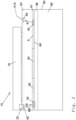
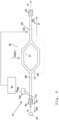
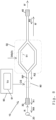
- Figures 1 and 2 show a first exemplary embodiment of an optical signal generator 10 according to the present invention.
- Figures 1 and 2 show a top view and a cross-section, respectively.
- the optical signal generator 10 comprises an optical emitter 20 that generates a beam of optical radiation R, a first beam deflecting element 30, a second beam deflecting element 40, and a modulator 50.
- the modulator 50 is located between the beam deflecting elements 30 and 40.
- the first and second beam deflecting elements 30 and 40 as well as the modulator 50 are located in the same plane E.
- the first and second beam deflecting elements 30, 40 and the modulator 50 share the same waveguiding silicon layer 61 of the same semiconductor chip 60.
- the semiconductor chip 60 may be based on SOI (silicon on insulator) material, which comprises a silicon substrate 65, a buried oxide layer 66 on top of the substrate 65, and a silicon layer on top of the buried oxide layer.
- SOI silicon on insulator
- the latter silicon layer preferably forms the waveguiding silicon layer 61.
- the emitter 20 may be a laser that is flip-chip mounted on the semiconductor chip 60.
- the emitter 20 may be mounted on the semiconductor chip 60 by means of a submount 70.
- the optical emitter 20 is preferably a continuous wave laser.
- the emitter's radiation R may be directed towards the first beam deflecting element 30 at an input angle between 10° and 30° with respect to the perpendicular of the plane E.
- the deflecting element 30 may be a grating that comprises a grating period for coupling the emitter's radiation into the plane E.
- the coupling efficiency of the first beam deflecting element 30 is preferably at least 30 % at the emitter's wavelength range and the input angle between 10° and 30°.
- the modulator 50 modulates the emitter's radiation R and outputs a modulated radiation R'.
- the modulator 50 modulates the emitter's radiation R in response to an external electrical data signal DS(D) that is applied to a carrier injection or depletion unit 51 (e. g. a pin-diode or pn-diode) of the modulator 50.
- the data signal DS(D) carries a data stream D.
- the electrical data signal DS(D) and the data rate of the data stream D may be in the GHz-range.
- the second beam deflecting element 40 is preferably a grating that has a grating period for out-of-plane coupling of the modulated radiation R' towards an output port A10 of the signal generator 10.
- the output angle is preferably between 10° and 30° with respect to the perpendicular of the plane E.
- the coupling efficiency of the second beam deflecting element 40 is preferably at least 30 % at the emitter's wavelength range and the output angle between 10° and 30°.
- a lens 62 may be located in the beam path between the emitter 20 and the first beam deflecting element 30.
- the lens 62 may be formed in at least one backend layer 63 of the backend of the semiconductor chip 60.
- a lens 64 may be located in the beam path between the second beam deflecting element 40 and the output port A10 of the signal generator 10.
- the lens 64 may be formed in the at least one backend layer 63 of the semiconductor chip 60.
- the optical signal generator 10 further comprises a phase shifter 80 and a control unit 90.
- the control unit 90 generates a control signal CS that controls the phase-shift that is induced by the phase shifter 80.
- the phase shifter 80 may comprise a thermal element capable of shifting the phase on the basis of the thermo-optic effect.
- the phase shifter 80 is located upstream the modulator 50, namely between the modulator 50 and the first beam deflecting element 30.
- the first beam deflecting element 30, the modulator 50 and the second beam deflecting element 40 may reflect radiation and generate reflected radiation RR.
- the reflected radiation RR may travel back to the emitter 20 and deteriorate the emission characteristic of the emitter 20.
- the control unit 90 In order to avoid or reduce reflected radiation RR or at least the impact of reflected radiation RR on the emitter's emission characteristic and the emitter's radiation R, the control unit 90 generates the control signal CS. Since the phase shifter 80 is located upstream the modulator 50, the phase shifter 80 can shift the phase of reflected radiation that is generated by both the second beam deflecting element 40 and the modulator 50.
- the phase shifter 80 can shift the phase such that the overlapped reflected radiations R2+R3 arrive at the emitter 20 with an optimal phase. This way of shifting the phase is particularly advantageous if one of the components, for instance the modulator 50 or the second beam deflecting element 40, causes most of the reflected radiation (i.e. R2 >> R1,R3 or R3 >> R1,R2).
- the cut-off frequency of the phase shifter 80 may be much smaller, for instance at least a thousand times smaller, than the cut-off frequency of the modulator 50.
- the optical signal generator 10 comprises a monitor detector 100 for generating a monitor signal MS that is proportional to the emitter's radiation R or at least characterizes the emitter's radiation R.
- the monitor detector 100 is connected to or coupled with a radiation path RP that extends from the first beam deflecting element 30 to the second beam deflecting element 40.
- the monitor detector detects just a small portion (preferably less than 10 %) of the emitter's radiation R.
- the coupling element 110 in Figure 1 is designed accordingly.
- the control unit 90 controls the phase-shift of the phase shifter 80 such that a predefined characteristic of the monitor signal MS and therefore of the emitter's radiation R remains inside a predefined range. For instance, the control unit 90 controls the phase-shift of the phase shifter 80 such that the intensity of the monitor signal MS remains inside a predefined intensity range.
- FIG 3 shows a second exemplary embodiment of an optical signal generator 10 according to the present invention.
- the optical signal generator 10 of Figure 3 comprises a bandpass filter that is located upstream the monitor detector 100.
- the bandpass filter has a center wavelength that corresponds to the center wavelength of the emitter's wavelength range.
- the bandpass filter makes sure that the impact of the control unit 90 and the impact of the phase shifter 80 is primarily directed towards the central wavelength of the emitter.
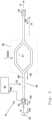
- Figure 4 shows a third exemplary embodiment of an optical signal generator 10 according to the present invention.
- the phase shifter 80 is located downstream the modulator 50, namely between the modulator 50 and the second beam deflecting element 40. Since the phase shifter 80 is located downstream the modulator 50, the phase shifter 80 can only shift the phase of reflected radiation R3 that is generated by the second beam deflecting element 40.
- the phase shifter 80 can shift the phase such that the radiation R3 arrives at the emitter 20 with an optimal phase. This way of shifting the phase is particularly advantageous if the second beam deflecting element 40 causes most of the reflected radiation (i.e. R3 >> R1 or R3 >> R2).
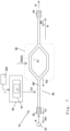
- Figure 5 shows a fourth exemplary embodiment of an optical signal generator 10 according to the present invention.
- the first beam deflecting element 30 has a monitor output.
- the monitor detector 100 is optically coupled with the monitor output.
- Figure 6 shows a fifth exemplary embodiment of an optical signal generator 10 according to the present invention.
- the second beam deflecting element 40 has a monitor output and the monitor detector 100 is optically coupled with the monitor output.
- Figure 7 shows a sixth exemplary embodiment of an optical signal generator 10 according to the present invention.
- the optical signal generator 10 comprises a temperature sensor 200 that is connected with the control unit 90.
- the control unit 90 controls the phase-shift of the phase shifter 80 as a function of a temperature value T that is provided by the temperature sensor 200.
- control unit 90 comprises a memory 91 that stores a look-up table LT.
- the look-up table LT defines a target phase-shift of the phase shifter 80 depending on the actual temperature value T of the temperature sensor 200.
- the control unit 90 generates the control signal CS according to the corresponding target value stored in the memory 91.
- the look-up table LT and its target phase-shifts have been determined and stored in the memory 91 during the fabrication of the optical signal generator 10.
- the target phase shifts are chosen such that any impact of reflected radiation RR on the emitter's emission characteristic is minimal.
- the emitter's emission characteristic may have been measured by an external monitor detector for different phase shifts and different temperatures.
- the optimal phase shifts may have been determined for each temperature within the possible temperature range of the optical signal generator 10.
- the optimal phase shifts and the corresponding control signals CS are stored in the memory 91.
- Figure 8 shows a seventh exemplary embodiment of an optical signal generator 10 according to the present invention.
- the optical signal generator 10 comprises a control unit 90 that generates an invariant control signal CS according to the corresponding target value TV stored in a memory 91.
- the target value TV has been determined and stored in the memory 91 during the fabrication of the optical signal generator 10.
- the target phase-shift is chosen such that the impact of reflected radiation RR on the emitter's emission characteristic is minimal.
- the emitter's emission characteristic may have been measured by an external monitor detector for different phase shifts. In this way, the optimal phase-shift may have been determined.
- the optimal phase shift, i.e. the target value TV, and the corresponding control signal CS are stored in the memory 91.
- the modulator 50 is a Mach-Zehnder modulator.
- the 1x2-couplers 52 and 53 (see Figure 1 ) at the input port and output port of the Mach-Zehnder modulator are preferably MMI (multi-mode interference) couplers.
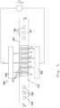
- Figure 9 shows an alternative embodiment of a modulator which can be used in the optical signal generators 10 according to Figures 1 -8 (instead of the Mach-Zehnder modulator). More specifically, Figure 9 shows an electro-optic modulator 500 that is configured for the modulation of the optical radiation R at a predetermined wavelength.
- the electro-optic modulator 500 has an optical resonator 510 in which a standing optical wave 511 can be formed for the predetermined wavelength.
- a SOI (silicon-on-insulator) waveguide 520 extends along the longitudinal direction of the resonator 510.
- the resonator 510 is delimited by mirror sections 530 and 531, which are formed by holes 540 in the SOI waveguide 520.
- p-doped semiconductor sections p and n-doped section n are arranged at a distance from one another. Each doped semiconductor section lies locally at an intensity minimum of the standing optical wave.
- a modulated voltage U By applying a modulated voltage U at contacts 550 a modulated current I is generated.
- the current I injects carriers which modulate the resonance wavelength of the resonator 510 and therefore the amplitude of the output radiation R'.
- the modulated voltage U may consist of a bias voltage and the external electrical data signal DS(D) (see Figure 10 ).
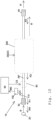
- Figure 10 shows an exemplary embodiment of an optical signal generators 10 that comprises the electro-optic modulator 500 of Figure 9 . Since the mirror sections 530 and 531 may generate a significant amount of reflected radiation R2, the phase shifter 80 is preferably located upstream the modulator 500.
Landscapes
- Physics & Mathematics (AREA)
- Nonlinear Science (AREA)
- Optics & Photonics (AREA)
- General Physics & Mathematics (AREA)
- Electromagnetism (AREA)
- Engineering & Computer Science (AREA)
- Computer Networks & Wireless Communication (AREA)
- Signal Processing (AREA)
- Condensed Matter Physics & Semiconductors (AREA)
- Optical Modulation, Optical Deflection, Nonlinear Optics, Optical Demodulation, Optical Logic Elements (AREA)
Claims (15)
- Optischer Signalgenerator (10), umfassend:- einen optischen Emitter (20), der dafür ausgelegt ist, einen Strahl optischer Strahlung, (R), zu erzeugen- ein erstes (30) und ein zweites (40) Strahlablenkungselement,- einen Modulator (50), der zwischen den Strahlablenkungselementen angeordnet ist,- einen den Phasenschieber (80), der zwischen den Strahlablenkungselementen angeordnet ist,- eine Steuereinheit (90), die dafür ausgelegt ist, die Phasenverschiebung des Phasenschiebers zu steuern,- wobei das erste und das zweite Strahlablenkungselement, der Phasenschieber und der Modulator in derselben Ebene angeordnet sind, (61)- wobei der durch den optischen Emitter erzeugte Strahl einen Winkel relativ zu dieser Ebene aufweist,- wobei das erste Strahlablenkungselement dafür ausgelegt ist, den Strahl (R) des Emitters in die Ebene zum Modulator abzulenken, wobei der Modulator dafür ausgelegt ist, die Strahlung des Emitters zu modulieren und eine modulierte Strahlung, (R'), auszugeben- wobei das zweite Strahlablenkungselement dafür ausgelegt ist, die modulierte Strahlung aus der Ebene zu einem Ausgangsport des Signalgenerators abzulenken,- wobei der Modulator dafür ausgelegt ist, die Strahlung des Emitters in Reaktion auf ein elektrisches Datensignal, das an den Modulator angelegt wird und einen Datenstrom umfasst, zu modulieren,- wobei die Steuereinheit dafür ausgelegt ist, ein Steuersignal zu erzeugen, um die Phasenverschiebung des Phasenschiebers zu steuern und um einen Einfluss von reflektierter Strahlung auf die Emissionscharakteristik des Emitters zu vermeiden oder zu reduzieren,- wobei der Signalgenerator einen Speicher umfasst, in dem ein Zielwert gespeichert ist, und- wobei eine Steuereinheit dafür ausgelegt ist, die Phasenverschiebung des Phasenschiebers gemäß dem gespeicherten Zielwert zu steuern.
- Optischer Signalgenerator gemäß Anspruch 1,- wobei eine optimale Phasenverschiebung des Phasenschiebers, die die reflektierte Strahlung oder deren Einfluss auf die Ausgangscharakteristik des Emitters vermeidet oder reduziert, während der Herstellung des Signalgenerators bestimmt wurde, und- wobei der Zielwert die optimale Phasenverschiebung des Phasenschiebers, eine optimale Steuerspannung, die die optimale Phasenverschiebung bewirkt, oder einen optimalen Steuerstrom, der die optimale Phasenverschiebung bewirkt, beschreibt.
- Optischer Signalgenerator gemäß Anspruch 1,
wobei die Grenzfrequenz des Phasenschiebers kleiner als die Grenzfrequenz des Modulators ist. - Optischer Signalgenerator gemäß Anspruch 3,
wobei die Grenzfrequenz des Phasenschiebers wenigstens tausendfach kleiner als die Grenzfrequenz des Modulators ist. - Optischer Signalgenerator gemäß Anspruch 1,- wobei der optische Signalgenerator einen Überwachungsdetektor (100) zum Erzeugen eines Überwachungssignals umfasst, das proportional zur Strahlung des Emitters ist oder wenigstens die Strahlung des Emitters charakterisiert, und- wobei die Steuereinheit dafür ausgelegt ist, die Phasenverschiebung des Phasenschiebers so zu steuern, dass eine vordefinierte Charakteristik des Überwachungssignals und damit der Strahlung des Emitters innerhalb eines vordefinierten Bereichs bleibt.
- Optischer Signalgenerator gemäß Anspruch 5,
wobei die Steuereinheit dafür ausgelegt ist, die Phasenverschiebung des Phasenschiebers so zu steuern, dass die Intensität des Überwachungssignals innerhalb eines vordefinierten Intensitätsbereichs bleibt. - Optischer Signalgenerator gemäß Anspruch 5,
wobei ein Bandpassfilter mit einer Zentralwellenlänge stromaufwärts des Überwachungsdetektors angeordnet ist. - Optischer Signalgenerator gemäß Anspruch 5,- wobei der Überwachungsdetektor mit einem Strahlungsweg verbunden oder gekoppelt ist, der sich vom ersten Strahlablenkungselement zum zweiten Strahlablenkungselement erstreckt, und- wobei der Überwachungsdetektor dafür ausgelegt ist, einen Teil der Strahlung des Emitters zu detektieren.
- Optischer Signalgenerator gemäß Anspruch 5,- wobei das erste oder das zweite Strahlablenkungselement einen Monitorausgang hat und- wobei der Überwachungsdetektor optisch mit dem Monitorausgang gekoppelt ist.
- Optischer Signalgenerator gemäß Anspruch 1,- wobei der Signalgenerator einen Temperatursensor umfasst und- wobei eine Steuereinheit dafür ausgelegt ist, die Phasenverschiebung des Phasenschiebers in Abhängigkeit von einem durch den Temperatursensor bereitgestellten Temperaturwert zu steuern.
- Optischer Signalgenerator gemäß Anspruch 10,- wobei der Signalgenerator einen Speicher umfasst, in dem eine Nachschlagetabelle gespeichert ist, die einen Zielwert definiert, der von dem tatsächlichen Temperaturwert des Temperatursensors abhängt, und- wobei der Zielwert die optimale Phasenverschiebung des Phasenschiebers, die optimale Steuerspannung, die die optimale Phasenverschiebung bewirkt, oder einen optimalen Steuerstrom, der die optimale Phasenverschiebung bewirkt, beschreibt.
- Optischer Signalgenerator gemäß Anspruch 1,
wobei wenigstens ein Phasenschieber stromabwärts des Modulators angeordnet und dafür ausgelegt ist, die Phase der Strahlung, die von dem zweiten Strahlablenkungselement reflektiert wird, zu verschieben. - Optischer Signalgenerator gemäß Anspruch 1,
wobei wenigstens ein Phasenschieber stromaufwärts des Modulators angeordnet und dafür ausgelegt ist, die Phase der Strahlung, die sowohl vom Modulator als auch dem zweiten Strahlablenkungselement reflektiert wird, zu verschieben. - Verfahren zum Herstellen eines optischen Signalgenerators, die Schritte umfassend:- Herstellen eines optischen Emitters, eines ersten und eines zweiten Strahlablenkungselements, eines Phasenschiebers, der zwischen den Strahlablenkungselementen angeordnet ist, und eines Modulators, der zwischen den Strahlablenkungselementen angeordnet ist,- wobei das erste und das zweite Strahlablenkungselement, der Phasenschieber und der Modulator in derselben Ebene angeordnet sind,- wobei der optische Emitter dafür ausgelegt ist, einen Strahl optischer Strahlung zu erzeugen, wobei der Strahl einen Winkel relativ zur Ebene aufweist,- wobei das erste Strahlablenkungselement dafür ausgelegt ist, den Strahl des Emitters in die Ebene zum Modulator abzulenken,- wobei der Modulator dafür ausgelegt ist, die Strahlung des Emitters zu modulieren und eine modulierte Strahlung auszugeben,- wobei das zweite Strahlablenkungselement dafür ausgelegt ist, die modulierte Strahlung aus der Ebene zu einem Ausgangsport des Signalgenerators abzulenken,- wobei während der Herstellung eine optimale Phase des Phasenschiebers bestimmt wird, die einen Einfluss der reflektierten Strahlung auf die Ausgangscharakteristik des Emitters vermeidet oder reduziert, und- wobei das entsprechende Steuersignal, das die optimale Phase für den Phasenschieber erzeugt, in einer Steuereinheit gespeichert ist.
- Verfahren nach Anspruch 14,
wobei während der Herstellung die optimale Phase, die einen Einfluss der reflektierten Strahlung auf die Ausgangscharakteristik des Emitters vermeidet oder reduziert, bei verschiedenen Temperaturen bestimmt wird und die entsprechenden Steuersignale für den Phasenschieber zur weiteren Verwendung in einer Nachschlagetabelle der Steuereinheit in Abhängigkeit von dem oder unter Bezugnahme auf den entsprechenden Temperaturwert gespeichert werden.
Applications Claiming Priority (2)
| Application Number | Priority Date | Filing Date | Title |
|---|---|---|---|
| US15/674,424 US10514584B2 (en) | 2017-08-10 | 2017-08-10 | Optical signal generator comprising a phase shifter |
| PCT/EP2018/070415 WO2019030019A1 (en) | 2017-08-10 | 2018-07-27 | Optical signal generator comprising a phase shifter |
Publications (2)
| Publication Number | Publication Date |
|---|---|
| EP3665751A1 EP3665751A1 (de) | 2020-06-17 |
| EP3665751B1 true EP3665751B1 (de) | 2023-09-27 |
Family
ID=63207718
Family Applications (1)
| Application Number | Title | Priority Date | Filing Date |
|---|---|---|---|
| EP18755142.9A Active EP3665751B1 (de) | 2017-08-10 | 2018-07-27 | Optischer signalgenerator mit einem phasenschieber |
Country Status (4)
| Country | Link |
|---|---|
| US (1) | US10514584B2 (de) |
| EP (1) | EP3665751B1 (de) |
| CN (1) | CN110959233B (de) |
| WO (1) | WO2019030019A1 (de) |
Families Citing this family (3)
| Publication number | Priority date | Publication date | Assignee | Title |
|---|---|---|---|---|
| US10509167B2 (en) * | 2018-04-23 | 2019-12-17 | Hewlett Packard Enterprise Development Lp | Optical phase difference calculation using analog processing |
| AU2023210287A1 (en) | 2022-01-21 | 2024-09-05 | Poseida Therapeutics, Inc. | Compositions and methods for delivery of nucleic acids |
| JP2025528163A (ja) | 2022-08-11 | 2025-08-26 | ポセイダ セラピューティクス,インコーポレイティド | キメラcd8-アルファ補助受容体組成物及び使用方法 |
Family Cites Families (18)
| Publication number | Priority date | Publication date | Assignee | Title |
|---|---|---|---|---|
| JPH09269428A (ja) | 1996-03-29 | 1997-10-14 | Nec Corp | 反射戻り光補償回路 |
| US6616353B1 (en) * | 1999-10-07 | 2003-09-09 | Massachusetts Institute Of Technology | Laser intensity noise suppression using unbalanced interferometer modulation |
| JP2003296979A (ja) * | 2002-01-31 | 2003-10-17 | Yasuo Cho | 誘電体記録媒体の記録条件抽出システム及び記録条件抽出方法並びに情報記録装置 |
| CN1997924B (zh) | 2004-04-15 | 2016-05-04 | 英飞聂拉股份有限公司 | 用于wdm传输网络的无制冷且波长栅格漂移的集成光路(pic) |
| US7512166B2 (en) | 2006-12-01 | 2009-03-31 | Raybit Systems | Apparatus and method for controlling optical power and extinction ratio |
| WO2008107963A1 (ja) | 2007-03-05 | 2008-09-12 | Fujitsu Limited | 光半導体素子 |
| US7805026B2 (en) * | 2007-10-09 | 2010-09-28 | Alcatel-Lucent Usa Inc. | Resonator-assisted control of radio-frequency response in an optical modulator |
| JP5293557B2 (ja) * | 2008-12-17 | 2013-09-18 | セイコーエプソン株式会社 | 超音波トランスデューサー、超音波トランスデューサーアレイ及び超音波デバイス |
| US9318868B2 (en) | 2011-09-07 | 2016-04-19 | Skorpios Technologies, Inc. | Tunable hybrid laser with carrier-induced phase control |
| JP2013543127A (ja) * | 2010-11-01 | 2013-11-28 | コチ・ウニヴェルシテシ | 小型で集積化されたマイクロエレクトロメカニカルシステム(メムス)の光学センサアレイ |
| KR101845514B1 (ko) * | 2010-12-17 | 2018-04-04 | 삼성전자주식회사 | 소형 광 변조기 및 이를 포함하는 광 송신기 |
| DE102011005422B4 (de) | 2011-03-11 | 2013-01-31 | Ihp Gmbh - Innovations For High Performance Microelectronics / Leibniz-Institut Für Innovative Mikroelektronik | Elektrooptischer Modulator |
| WO2013133099A1 (ja) | 2012-03-08 | 2013-09-12 | 独立行政法人産業技術総合研究所 | 光源回路及びこれを備えた光源装置 |
| WO2014156885A1 (ja) | 2013-03-25 | 2014-10-02 | 技術研究組合光電子融合基盤技術研究所 | 光回路 |
| CN107111060A (zh) | 2014-07-14 | 2017-08-29 | 拜奥德光电公司 | 与光耦合元件的3d光子集成 |
| DE102015208983A1 (de) | 2015-05-15 | 2016-11-17 | Technische Universität Berlin | Optoelektronisches Bauelement |
| JP6628028B2 (ja) | 2015-10-01 | 2020-01-08 | 富士通株式会社 | 半導体発光装置及び光送受信器 |
| US20170250755A1 (en) | 2016-02-29 | 2017-08-31 | Renesas Electronics Corporation | Semiconductor device |
-
2017
- 2017-08-10 US US15/674,424 patent/US10514584B2/en active Active
-
2018
- 2018-07-27 CN CN201880049510.4A patent/CN110959233B/zh active Active
- 2018-07-27 EP EP18755142.9A patent/EP3665751B1/de active Active
- 2018-07-27 WO PCT/EP2018/070415 patent/WO2019030019A1/en not_active Ceased
Also Published As
| Publication number | Publication date |
|---|---|
| CN110959233B (zh) | 2023-04-04 |
| CN110959233A (zh) | 2020-04-03 |
| EP3665751A1 (de) | 2020-06-17 |
| WO2019030019A1 (en) | 2019-02-14 |
| US20190049816A1 (en) | 2019-02-14 |
| US10514584B2 (en) | 2019-12-24 |
Similar Documents
| Publication | Publication Date | Title |
|---|---|---|
| JP5206187B2 (ja) | 光半導体装置 | |
| JP5315792B2 (ja) | 光変調器 | |
| US6480513B1 (en) | Tunable external cavity laser | |
| JP5850139B2 (ja) | 光半導体デバイス | |
| RU2317575C2 (ru) | Электроабсорбционный модулятор с широкой оптической полосой и способ модуляции оптического сигнала | |
| EP3703202B1 (de) | Abstimmbare laservorrichtung und lasersender | |
| CN104937791B (zh) | 激光装置、光调制装置以及光半导体元件 | |
| TW202333430A (zh) | 提供一寬頻啁啾雷射訊號的方法、可調頻固態雷射裝置及高解析度快速響應光達成像系統 | |
| US20120057079A1 (en) | Method and system for hybrid integration of a tunable laser for a cable tv transmitter | |
| KR101781011B1 (ko) | 파면 합성기 시스템 | |
| US6920253B2 (en) | Optical modulator based on a microdisk resonator | |
| US8885679B1 (en) | Mode-hop free athermal laser | |
| JP2010008763A (ja) | 光変調デバイス及び光半導体装置 | |
| JP2008268276A (ja) | 光変調器、光源装置及び前記光変調器の駆動方法 | |
| US10514584B2 (en) | Optical signal generator comprising a phase shifter | |
| KR20010013957A (ko) | 광학 방사선 스위칭, 증폭, 제어 및 변조 방법 및 장치 | |
| JP2009145838A (ja) | レーザビーム走査装置 | |
| US8805126B2 (en) | Photonic modulator with forward-and reverse-biased diodes for separate tuning and modulating elements | |
| US10707837B2 (en) | Laser frequency chirping structures, methods, and applications | |
| KR20210059472A (ko) | 라이다 장치 | |
| US9817295B2 (en) | Injection modulator | |
| JP2000294870A (ja) | 発光デバイス | |
| US20240372314A1 (en) | Optical modulation chip and tunable laser | |
| KR100299121B1 (ko) | 광스위치및광스위칭방법 | |
| Rabus et al. | Devices |
Legal Events
| Date | Code | Title | Description |
|---|---|---|---|
| STAA | Information on the status of an ep patent application or granted ep patent |
Free format text: STATUS: UNKNOWN |
|
| STAA | Information on the status of an ep patent application or granted ep patent |
Free format text: STATUS: THE INTERNATIONAL PUBLICATION HAS BEEN MADE |
|
| PUAI | Public reference made under article 153(3) epc to a published international application that has entered the european phase |
Free format text: ORIGINAL CODE: 0009012 |
|
| STAA | Information on the status of an ep patent application or granted ep patent |
Free format text: STATUS: REQUEST FOR EXAMINATION WAS MADE |
|
| 17P | Request for examination filed |
Effective date: 20200224 |
|
| AK | Designated contracting states |
Kind code of ref document: A1 Designated state(s): AL AT BE BG CH CY CZ DE DK EE ES FI FR GB GR HR HU IE IS IT LI LT LU LV MC MK MT NL NO PL PT RO RS SE SI SK SM TR |
|
| AX | Request for extension of the european patent |
Extension state: BA ME |
|
| DAV | Request for validation of the european patent (deleted) | ||
| DAX | Request for extension of the european patent (deleted) | ||
| GRAP | Despatch of communication of intention to grant a patent |
Free format text: ORIGINAL CODE: EPIDOSNIGR1 |
|
| STAA | Information on the status of an ep patent application or granted ep patent |
Free format text: STATUS: GRANT OF PATENT IS INTENDED |
|
| INTG | Intention to grant announced |
Effective date: 20230509 |
|
| GRAS | Grant fee paid |
Free format text: ORIGINAL CODE: EPIDOSNIGR3 |
|
| GRAA | (expected) grant |
Free format text: ORIGINAL CODE: 0009210 |
|
| STAA | Information on the status of an ep patent application or granted ep patent |
Free format text: STATUS: THE PATENT HAS BEEN GRANTED |
|
| AK | Designated contracting states |
Kind code of ref document: B1 Designated state(s): AL AT BE BG CH CY CZ DE DK EE ES FI FR GB GR HR HU IE IS IT LI LT LU LV MC MK MT NL NO PL PT RO RS SE SI SK SM TR |
|
| REG | Reference to a national code |
Ref country code: GB Ref legal event code: FG4D |
|
| REG | Reference to a national code |
Ref country code: CH Ref legal event code: EP |
|
| REG | Reference to a national code |
Ref country code: DE Ref legal event code: R096 Ref document number: 602018058299 Country of ref document: DE |
|
| REG | Reference to a national code |
Ref country code: IE Ref legal event code: FG4D |
|
| REG | Reference to a national code |
Ref country code: LT Ref legal event code: MG9D |
|
| PG25 | Lapsed in a contracting state [announced via postgrant information from national office to epo] |
Ref country code: GR Free format text: LAPSE BECAUSE OF FAILURE TO SUBMIT A TRANSLATION OF THE DESCRIPTION OR TO PAY THE FEE WITHIN THE PRESCRIBED TIME-LIMIT Effective date: 20231228 |
|
| PG25 | Lapsed in a contracting state [announced via postgrant information from national office to epo] |
Ref country code: SE Free format text: LAPSE BECAUSE OF FAILURE TO SUBMIT A TRANSLATION OF THE DESCRIPTION OR TO PAY THE FEE WITHIN THE PRESCRIBED TIME-LIMIT Effective date: 20230927 Ref country code: RS Free format text: LAPSE BECAUSE OF FAILURE TO SUBMIT A TRANSLATION OF THE DESCRIPTION OR TO PAY THE FEE WITHIN THE PRESCRIBED TIME-LIMIT Effective date: 20230927 Ref country code: NO Free format text: LAPSE BECAUSE OF FAILURE TO SUBMIT A TRANSLATION OF THE DESCRIPTION OR TO PAY THE FEE WITHIN THE PRESCRIBED TIME-LIMIT Effective date: 20231227 Ref country code: LV Free format text: LAPSE BECAUSE OF FAILURE TO SUBMIT A TRANSLATION OF THE DESCRIPTION OR TO PAY THE FEE WITHIN THE PRESCRIBED TIME-LIMIT Effective date: 20230927 Ref country code: LT Free format text: LAPSE BECAUSE OF FAILURE TO SUBMIT A TRANSLATION OF THE DESCRIPTION OR TO PAY THE FEE WITHIN THE PRESCRIBED TIME-LIMIT Effective date: 20230927 Ref country code: HR Free format text: LAPSE BECAUSE OF FAILURE TO SUBMIT A TRANSLATION OF THE DESCRIPTION OR TO PAY THE FEE WITHIN THE PRESCRIBED TIME-LIMIT Effective date: 20230927 Ref country code: GR Free format text: LAPSE BECAUSE OF FAILURE TO SUBMIT A TRANSLATION OF THE DESCRIPTION OR TO PAY THE FEE WITHIN THE PRESCRIBED TIME-LIMIT Effective date: 20231228 Ref country code: FI Free format text: LAPSE BECAUSE OF FAILURE TO SUBMIT A TRANSLATION OF THE DESCRIPTION OR TO PAY THE FEE WITHIN THE PRESCRIBED TIME-LIMIT Effective date: 20230927 |
|
| REG | Reference to a national code |
Ref country code: NL Ref legal event code: MP Effective date: 20230927 |
|
| REG | Reference to a national code |
Ref country code: AT Ref legal event code: MK05 Ref document number: 1616351 Country of ref document: AT Kind code of ref document: T Effective date: 20230927 |
|
| PG25 | Lapsed in a contracting state [announced via postgrant information from national office to epo] |
Ref country code: NL Free format text: LAPSE BECAUSE OF FAILURE TO SUBMIT A TRANSLATION OF THE DESCRIPTION OR TO PAY THE FEE WITHIN THE PRESCRIBED TIME-LIMIT Effective date: 20230927 |
|
| PG25 | Lapsed in a contracting state [announced via postgrant information from national office to epo] |
Ref country code: IS Free format text: LAPSE BECAUSE OF FAILURE TO SUBMIT A TRANSLATION OF THE DESCRIPTION OR TO PAY THE FEE WITHIN THE PRESCRIBED TIME-LIMIT Effective date: 20240127 |
|
| PG25 | Lapsed in a contracting state [announced via postgrant information from national office to epo] |
Ref country code: AT Free format text: LAPSE BECAUSE OF FAILURE TO SUBMIT A TRANSLATION OF THE DESCRIPTION OR TO PAY THE FEE WITHIN THE PRESCRIBED TIME-LIMIT Effective date: 20230927 |
|
| PG25 | Lapsed in a contracting state [announced via postgrant information from national office to epo] |
Ref country code: ES Free format text: LAPSE BECAUSE OF FAILURE TO SUBMIT A TRANSLATION OF THE DESCRIPTION OR TO PAY THE FEE WITHIN THE PRESCRIBED TIME-LIMIT Effective date: 20230927 |
|
| PG25 | Lapsed in a contracting state [announced via postgrant information from national office to epo] |
Ref country code: SM Free format text: LAPSE BECAUSE OF FAILURE TO SUBMIT A TRANSLATION OF THE DESCRIPTION OR TO PAY THE FEE WITHIN THE PRESCRIBED TIME-LIMIT Effective date: 20230927 Ref country code: RO Free format text: LAPSE BECAUSE OF FAILURE TO SUBMIT A TRANSLATION OF THE DESCRIPTION OR TO PAY THE FEE WITHIN THE PRESCRIBED TIME-LIMIT Effective date: 20230927 Ref country code: IS Free format text: LAPSE BECAUSE OF FAILURE TO SUBMIT A TRANSLATION OF THE DESCRIPTION OR TO PAY THE FEE WITHIN THE PRESCRIBED TIME-LIMIT Effective date: 20240127 Ref country code: ES Free format text: LAPSE BECAUSE OF FAILURE TO SUBMIT A TRANSLATION OF THE DESCRIPTION OR TO PAY THE FEE WITHIN THE PRESCRIBED TIME-LIMIT Effective date: 20230927 Ref country code: EE Free format text: LAPSE BECAUSE OF FAILURE TO SUBMIT A TRANSLATION OF THE DESCRIPTION OR TO PAY THE FEE WITHIN THE PRESCRIBED TIME-LIMIT Effective date: 20230927 Ref country code: CZ Free format text: LAPSE BECAUSE OF FAILURE TO SUBMIT A TRANSLATION OF THE DESCRIPTION OR TO PAY THE FEE WITHIN THE PRESCRIBED TIME-LIMIT Effective date: 20230927 Ref country code: AT Free format text: LAPSE BECAUSE OF FAILURE TO SUBMIT A TRANSLATION OF THE DESCRIPTION OR TO PAY THE FEE WITHIN THE PRESCRIBED TIME-LIMIT Effective date: 20230927 Ref country code: PT Free format text: LAPSE BECAUSE OF FAILURE TO SUBMIT A TRANSLATION OF THE DESCRIPTION OR TO PAY THE FEE WITHIN THE PRESCRIBED TIME-LIMIT Effective date: 20240129 Ref country code: SK Free format text: LAPSE BECAUSE OF FAILURE TO SUBMIT A TRANSLATION OF THE DESCRIPTION OR TO PAY THE FEE WITHIN THE PRESCRIBED TIME-LIMIT Effective date: 20230927 |
|
| PG25 | Lapsed in a contracting state [announced via postgrant information from national office to epo] |
Ref country code: PL Free format text: LAPSE BECAUSE OF FAILURE TO SUBMIT A TRANSLATION OF THE DESCRIPTION OR TO PAY THE FEE WITHIN THE PRESCRIBED TIME-LIMIT Effective date: 20230927 Ref country code: IT Free format text: LAPSE BECAUSE OF FAILURE TO SUBMIT A TRANSLATION OF THE DESCRIPTION OR TO PAY THE FEE WITHIN THE PRESCRIBED TIME-LIMIT Effective date: 20230927 |
|
| REG | Reference to a national code |
Ref country code: DE Ref legal event code: R097 Ref document number: 602018058299 Country of ref document: DE |
|
| PG25 | Lapsed in a contracting state [announced via postgrant information from national office to epo] |
Ref country code: DK Free format text: LAPSE BECAUSE OF FAILURE TO SUBMIT A TRANSLATION OF THE DESCRIPTION OR TO PAY THE FEE WITHIN THE PRESCRIBED TIME-LIMIT Effective date: 20230927 |
|
| PG25 | Lapsed in a contracting state [announced via postgrant information from national office to epo] |
Ref country code: DK Free format text: LAPSE BECAUSE OF FAILURE TO SUBMIT A TRANSLATION OF THE DESCRIPTION OR TO PAY THE FEE WITHIN THE PRESCRIBED TIME-LIMIT Effective date: 20230927 |
|
| PLBE | No opposition filed within time limit |
Free format text: ORIGINAL CODE: 0009261 |
|
| STAA | Information on the status of an ep patent application or granted ep patent |
Free format text: STATUS: NO OPPOSITION FILED WITHIN TIME LIMIT |
|
| 26N | No opposition filed |
Effective date: 20240628 |
|
| PG25 | Lapsed in a contracting state [announced via postgrant information from national office to epo] |
Ref country code: SI Free format text: LAPSE BECAUSE OF FAILURE TO SUBMIT A TRANSLATION OF THE DESCRIPTION OR TO PAY THE FEE WITHIN THE PRESCRIBED TIME-LIMIT Effective date: 20230927 |
|
| PG25 | Lapsed in a contracting state [announced via postgrant information from national office to epo] |
Ref country code: SI Free format text: LAPSE BECAUSE OF FAILURE TO SUBMIT A TRANSLATION OF THE DESCRIPTION OR TO PAY THE FEE WITHIN THE PRESCRIBED TIME-LIMIT Effective date: 20230927 |
|
| PG25 | Lapsed in a contracting state [announced via postgrant information from national office to epo] |
Ref country code: BG Free format text: LAPSE BECAUSE OF FAILURE TO SUBMIT A TRANSLATION OF THE DESCRIPTION OR TO PAY THE FEE WITHIN THE PRESCRIBED TIME-LIMIT Effective date: 20230927 |
|
| PG25 | Lapsed in a contracting state [announced via postgrant information from national office to epo] |
Ref country code: BG Free format text: LAPSE BECAUSE OF FAILURE TO SUBMIT A TRANSLATION OF THE DESCRIPTION OR TO PAY THE FEE WITHIN THE PRESCRIBED TIME-LIMIT Effective date: 20230927 |
|
| PG25 | Lapsed in a contracting state [announced via postgrant information from national office to epo] |
Ref country code: MC Free format text: LAPSE BECAUSE OF FAILURE TO SUBMIT A TRANSLATION OF THE DESCRIPTION OR TO PAY THE FEE WITHIN THE PRESCRIBED TIME-LIMIT Effective date: 20230927 |
|
| REG | Reference to a national code |
Ref country code: CH Ref legal event code: PL |
|
| PG25 | Lapsed in a contracting state [announced via postgrant information from national office to epo] |
Ref country code: LU Free format text: LAPSE BECAUSE OF NON-PAYMENT OF DUE FEES Effective date: 20240727 |
|
| PG25 | Lapsed in a contracting state [announced via postgrant information from national office to epo] |
Ref country code: LU Free format text: LAPSE BECAUSE OF NON-PAYMENT OF DUE FEES Effective date: 20240727 |
|
| PG25 | Lapsed in a contracting state [announced via postgrant information from national office to epo] |
Ref country code: CH Free format text: LAPSE BECAUSE OF NON-PAYMENT OF DUE FEES Effective date: 20240731 Ref country code: BE Free format text: LAPSE BECAUSE OF NON-PAYMENT OF DUE FEES Effective date: 20240731 |
|
| REG | Reference to a national code |
Ref country code: BE Ref legal event code: MM Effective date: 20240731 |
|
| PG25 | Lapsed in a contracting state [announced via postgrant information from national office to epo] |
Ref country code: IE Free format text: LAPSE BECAUSE OF NON-PAYMENT OF DUE FEES Effective date: 20240727 |
|
| PGFP | Annual fee paid to national office [announced via postgrant information from national office to epo] |
Ref country code: DE Payment date: 20250731 Year of fee payment: 8 |
|
| PGFP | Annual fee paid to national office [announced via postgrant information from national office to epo] |
Ref country code: GB Payment date: 20250724 Year of fee payment: 8 |
|
| PGFP | Annual fee paid to national office [announced via postgrant information from national office to epo] |
Ref country code: FR Payment date: 20250723 Year of fee payment: 8 |
|
| PG25 | Lapsed in a contracting state [announced via postgrant information from national office to epo] |
Ref country code: CY Free format text: LAPSE BECAUSE OF FAILURE TO SUBMIT A TRANSLATION OF THE DESCRIPTION OR TO PAY THE FEE WITHIN THE PRESCRIBED TIME-LIMIT; INVALID AB INITIO Effective date: 20180727 |
|
| PG25 | Lapsed in a contracting state [announced via postgrant information from national office to epo] |
Ref country code: HU Free format text: LAPSE BECAUSE OF FAILURE TO SUBMIT A TRANSLATION OF THE DESCRIPTION OR TO PAY THE FEE WITHIN THE PRESCRIBED TIME-LIMIT; INVALID AB INITIO Effective date: 20180727 |