EP3571817B1 - Treiber für hochschwingenden sender mit spannungsverstärker - Google Patents
Treiber für hochschwingenden sender mit spannungsverstärker Download PDFInfo
- Publication number
- EP3571817B1 EP3571817B1 EP18747203.0A EP18747203A EP3571817B1 EP 3571817 B1 EP3571817 B1 EP 3571817B1 EP 18747203 A EP18747203 A EP 18747203A EP 3571817 B1 EP3571817 B1 EP 3571817B1
- Authority
- EP
- European Patent Office
- Prior art keywords
- transmitter
- driver
- transmitter driver
- high frequency
- boost
- Prior art date
- Legal status (The legal status is an assumption and is not a legal conclusion. Google has not performed a legal analysis and makes no representation as to the accuracy of the status listed.)
- Active
Links
Images





Classifications
-
- H—ELECTRICITY
- H04—ELECTRIC COMMUNICATION TECHNIQUE
- H04L—TRANSMISSION OF DIGITAL INFORMATION, e.g. TELEGRAPHIC COMMUNICATION
- H04L25/00—Baseband systems
- H04L25/02—Details ; arrangements for supplying electrical power along data transmission lines
- H04L25/0264—Arrangements for coupling to transmission lines
- H04L25/0272—Arrangements for coupling to multiple lines, e.g. for differential transmission
-
- H—ELECTRICITY
- H04—ELECTRIC COMMUNICATION TECHNIQUE
- H04L—TRANSMISSION OF DIGITAL INFORMATION, e.g. TELEGRAPHIC COMMUNICATION
- H04L25/00—Baseband systems
- H04L25/02—Details ; arrangements for supplying electrical power along data transmission lines
- H04L25/0264—Arrangements for coupling to transmission lines
- H04L25/0298—Arrangement for terminating transmission lines
-
- H—ELECTRICITY
- H04—ELECTRIC COMMUNICATION TECHNIQUE
- H04L—TRANSMISSION OF DIGITAL INFORMATION, e.g. TELEGRAPHIC COMMUNICATION
- H04L27/00—Modulated-carrier systems
- H04L27/02—Amplitude-modulated carrier systems, e.g. using on-off keying; Single sideband or vestigial sideband modulation
- H04L27/04—Modulator circuits; Transmitter circuits
Definitions
- the present disclosure is related to transmitter drivers, in particular transmitter drivers for high speed transmission.
- Pulse amplitude modulation is a form of signal modulation where bit values are encoded in the amplitude of signal pulses.
- PAM4 is a form of PAM in which four distinct amplitude levels are used, each amplitude level encoding a different combination of two bits.
- PAM4 signaling has shown promise for high speed signaling (e.g., greater than 56 Gbps), compared to non-return to zero (NRZ) signaling.
- FIR finite impulse response
- US2009296851 A1 discloses a pre-emphasis circuit on a transmission side in a data transmission system, which includes transition detection circuits, a current switch circuit, and a current adder circuit, where the transition detection circuits detect transitions of transmission data signals, and outputting pulse signals at that time; where the current adder circuit receives detection signals from the transition detection circuits. Since the transition detection circuit has a high pass filter characteristic, when the current adder circuit is driven via the transition detection circuits, a gain is previously added by the transition detection circuits in the transition of the high frequency band of the transmission data signal.
- the proposed pre-emphasis circuit can be used for compensating the deterioration of communication quality in the high frequency due to the signal attenuation in the transmission line of the data transmission system.
- the transition detection circuit is configured with a capacitor whose capacitance value is variable or fixed and a resistor whose resistance value is variable or fixed.
- the present disclosure describes a circuit for increasing the bandwidth of a transmitter driver, without directly loading the transmitter output.
- a continuous time high-pass filter response is added to the transmitter output, using an AC-coupled feed-forward path.
- the capacitor-coupled path causes the voltage at the current source to change, such that more current is injected to the output at data transmission. This additional current helps to boost the voltage of high frequency signals, and has little or no effect on low frequency signals.
- the transmitter driver includes control switches to enable the bandwidth to be adapted for different data rates.
- a transmitter driver comprising a first voltage mode driver coupled to receive a first differential input signal from a first input port of the transmitter driver, and coupled to provide a first differential output signal at a first output port of the transmitter driver.
- the driver further comprises a second voltage mode driver coupled to receive a second differential input signal from a second input port of the transmitter driver, and coupled to provide a second differential output signal at a second output port of the transmitter driver.
- the driver further comprises a secondary data path having first input and output ports connected in parallel with the first voltage mode driver, and having second input and output ports connected in parallel with the second voltage mode driver, the secondary data path receiving boost current from a current source.
- the driver comprises a high frequency booster connected to the first and second input ports of the transmitter driver, and connected between the current source and the secondary data path, the high frequency booster providing a high frequency path for the boost current from the current source.
- a transmitter for transmitting differential signals comprising a transmitter driver including a first voltage mode driver coupled to receive a first differential input signal from a first input port of the transmitter driver, and coupled to provide a first differential output signal at a first output port of the transmitter driver.
- the transmitter also comprises a second voltage mode driver coupled to receive a second differential input signal from a second input port of the transmitter driver, and coupled to provide a second differential output signal at a second output port of the transmitter driver.
- the transmitter further comprises a secondary data path having first input and output ports connected in parallel with the first voltage mode driver, and having second input and output ports connected in parallel with the second voltage mode driver, the secondary data path receiving boost current from a current source.
- the transmitter comprises a high frequency booster connected to the first and second input ports of the transmitter driver, and connected between the current source and the secondary data path, the high frequency booster providing a high frequency path for the boost current from the current source; and a processor coupled to the transmitter driver for controlling operation of the transmitter driver.
- the high frequency booster comprises a respective RC network connected to each of the first and second input ports of the transmitter driver to provide the high frequency path, each of the RC networks including a feedforward capacitor and a resistor.
- the resistor of each RC network is a variable resistor.
- resistance of each variable resistor is controllably variable in the range of about 0 ohms to about 1000 ohms.
- capacitance of each feedforward capacitor is in the range of about lOfF to about 100fF.
- each feedforward capacitor is a variable capacitor.
- this implementation further comprises a first set of control switches connected to the high frequency booster to enable or disable the high frequency path.
- this implementation further comprises a second set of control switches connected to the secondary data path to enable or disable receiving of the boost current.
- the transmitter is coupled to a receiver via differential communication lines.
- Examples described herein may be implemented in a high speed (e.g., 56 Gbps or higher) communication system.
- Other applications may include other communication systems and transmitters that would benefit from a transmission boost at high frequencies.
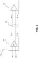
- FIG. 1 is a schematic diagram of an example high speed communication system 100, including a transmitter 102 and a receiver 104.
- the transmitter transmits differential signals to the receiver over differential communication lines 106.
- the use of differential signals may help to reduce the level of noise in signals received by the receiver 104, particularly where there is greater distance between the transmitter 102 and the receiver 104.
- the transmitter 102 includes a transmitter driver 108.
- the transmitter driver 108 may include more than one circuit component, as discussed further below.
- the transmitter 102 may include other components in addition to the transmitter driver 108.
- the transmitter 102 receives input data signals at transmitter input ports D0 and D0b, and outputs differential signals at transmitter output ports Tx_m and Tx_p.
- the differential signals are transmitted over the differential communication lines 106 and received by the receiver 104 at receiver input ports Rx_m and Rx_p.
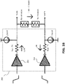
- FIG. 2A is a simplified diagram illustrating a source-series-terminated (SST) transmitter driver 200
- FIG. 2B shows the SST transmitter driver 200 with a DC voltage boost.
- first and second voltage mode transmitters 202, 204 are connected to respective resistors Rout_TX (assuming fixed output resistance).
- the voltage mode transmitters 202, 204 each receive respective differential input signals, as shown.
- the current from each voltage mode transmitter 202, 204 is I_sst.
- Far-end termination resistors are shown as Rtermination, and the output signals of the transmitter driver 200 are the differential signals at Voutp and Voutm.
- a DC current boost may be added, as shown in FIG. 2B , where a current source I_boost is connected to the outputs of each voltage mode transmitter 202, 204.
- I_boost the total current the transmitter driver 200 delivers to the termination resistors Rtermination is I_sst + I_boost.
- the DC voltage boost at the output Voutp and Voutm is dependent on the values of Rout_TX, Rtermination and I_boost. In the case were Rout_TX and Rtermination have the same resistance R, the voltage swing boost achieved is 2 ⁇ I_boost ⁇ R.
- I_boost (mA) Vswing (Vppd) V_boost (mV) 0 1 0 2.2 1.2 220 3.3 1.3 330 where Vswing is the peak-to-peak voltage of the voltage output and V_boost is the additional voltage boost resulting from I_boost (that is, the additional peak-to-peak voltage of Vswing provided by I_boost, compared to the case where I_boost is 0mA).
- the voltage boost provided is a DC voltage boost, meaning that it is not specific to high frequency output. Because a current boost gives rise to an output voltage boost, in the present disclosure both the terms “current boost” and “voltage boost” may be used interchangeably, and the term “boost” may be used generally to refer to both current boost and voltage boost.
- a high frequency boost may generally refer to current and voltage boost for high frequency input signals (e.g., signals at frequencies up to 14GHz).
- a high frequency boost may be observed as a transient boost in signal amplitude at the top of a rise in a pulse signal, and this boost at the top of a rise may be referred to as "peaking".
- FIG. 3 shows a schematic diagram of an example circuit 300 for the transmitter driver, in which a high frequency voltage boost is enabled.
- the circuit 300 includes first and second voltage mode transmitters 302, 304 (which may also be referred to collectively as differential voltage mode transmitters 302, 304) and a secondary data path 306 connected in parallel.
- the first voltage mode transmitter 302 is coupled to the input port D0 of the transmitter driver, to receive a first differential input signal, and coupled to the output port Tx_m of the transmitter driver, to output a first differential output signal.
- the second voltage mode transmitter 304 is coupled to the input port D0b of the transmitter driver, to receive a second differential input signal, and coupled to the output port Tx_p of the transmitter driver, to output a second differential output signal.
- each of the first and second voltage mode transmitters 302, 304 includes an inverter 308 and a resistor 310.
- Each inverter 308 receives input from the input port D0, D0b, respectively, and is coupled to the output port Tx_m, Tx_p, respectively, via the respective resistor 310.
- the resistance value of each of the resistor 310 may be selected to match the expected impedance of the transmission line coupled to the output ports Tx_m, Tx_p.
- the resistors 310 may each have a resistance of 50 ohms
- the secondary data path 306 has first input and output ports connected in parallel with the first voltage mode transmitter 302, and second input and output ports connected in parallel with the second voltage mode transmitter 304.
- the secondary data path 306 includes a first transistor differential pair, formed by a first pair of PMOS transistors 312. The gate of each of the PMOS transistors 312 is connected to the input port D0, D0b, respectively, and the drain of each PMOS transistor 312 is connected to the output port Tx_m, Tx_p, respectively.
- the secondary data path 306 drives the same output as the voltage mode transmitters 302, 304.
- the secondary data path 306 also includes a second transistor differential pair, formed by a second pair of PMOS transistors 314. The second pair of PMOS transistors 314 is connected to transistor current source.
- the secondary data path 306 receives a boost current from a DC current source 326.
- the boost current provided by the DC current source 326 results in a boost at the output ports Tx_m, Tx_p.
- the example circuit 300 also includes a high frequency booster 320.
- the high frequency booster is connected to the input ports D0, D0b, and is connected between the current source 326 and the secondary data path 306.
- the current or drive strength of the secondary data path 306 is determined by the high frequency booster 320.
- the high frequency booster 320 provides a high frequency path for the boost current, enabling a high frequency boost at the output ports Tx_m, Tx_p.
- the high frequency booster 320 also enables adjustment of the high frequency boost, via variable resistors, described below.
- the boost current from the current source 326 is split into two currents to the first pair of PMOS transistors 312 of the secondary data path 306.
- the high frequency path is provided by a RC network for each of the two differential signals.
- Each RC network includes a feedforward capacitor 322 and a variable resistor 324.
- the feedforward capacitor 322 is connected between each transmitter input port D0, D0b and the source terminal of the first pair of PMOS transistors 312.
- the feedforward capacitor 322 may have capacitance in the range of about lOfF to about 100fF and the variable resistor 324 may have resistance variable between about 0 ohms to about 1000 ohms, for example.
- the addition of the feedforward capacitors 322 provides a path for additional boost current at high frequencies.
- the variable resistors 324 are connected between the feedforward capacitors 322 and a bias voltage for the PMOS transistors 312.
- the variable resistors 324 are controllable (e.g., via a control signal from a processor (not shown)) to adjust the resistance value of the variable resistors 324, which may enable adjustment of the settling time of the boost current.
- the peaking frequency may be tuned by adjusting the values of at least one of the feedforward capacitors 322 and the variable resistors 324.
- the resistance of the variable resistors 324 may be adjusted dynamically. Simulation results discussed further below illustrate how varying the variable resistors 324 affects the output response.
- the addition of the high frequency booster 320 introduces relatively little overhead to the circuit 300 for the transmitter driver 108.
- the feedforward capacitors 322 may be variable capacitors, which may be controllable (e.g., via a control signal from a processor (not shown)) to adjust the capacitance values.
- the ability to control and adjust the capacitance values of the feedforward capacitors 322 may enable additional control of the high frequency response.
- FIG. 4 is a schematic diagram of another example circuit 400 for the transmitter driver 108.
- the example circuit 400 is similar to the circuit 300 of FIG. 3 , with the addition of control switches 402, 404 to control whether or not voltage boost at at least one of DC and high frequency is enabled.
- the operation of the control switches 402, 404 may be controlled via control signals from a processor (not shown), for example.
- the control switches 402, 404 may be turned on or off dynamically.
- the first set of control switches 402 is provided in the high frequency booster 320, to control whether there is high frequency boost provided.
- the second set of control switches 404 is provided at the gates of the first and second pairs of transistors 312, 314, to control whether there is any voltage boost provided.
- the second set of control switches 404 are all turned off, the current path for the boost current is open and no boost current (and hence no voltage boost) is enabled.
- both sets of control switches 402, 404 When both sets of control switches 402, 404 are turned off, no path is provided for the boost current, and the transmitter driver 108 operates without any voltage boost.
- the first set of control switches 402 When the first set of control switches 402 is turned off and the second set of control switches 404 is turned on, only a DC path is provided for the boost current, and the output of the transmitter driver 108 is provided with a DC voltage boost, but without high frequency voltage boost.
- the circuit 400 functions equivalently to the circuit 300 of FIG. 3 , where both DC and high frequency voltage boost are enabled.
- the transistors 312, 314 are off and no DC voltage boost is provided. In some examples, only the first set of control switches 402 may be provided, such that the DC voltage boost is always enabled but the high frequency voltage boost can be enabled or disabled.
- the example circuit 400 may help to lower power consumption at low data rates, where the benefits of the high frequency boost may not be needed.
- simulation results are now discussed. It should be understood that these simulation results are provided for the purpose of illustration only, and are not intended to be limiting or promissory.
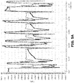
- FIGS. 5A and 5B show simulation results for the example circuit 400 of FIG. 4 , with only DC boost (grey solid line) and with additional high frequency boost (black dotted line).
- FIG. 5A shows the current at location ID indicated in FIG. 4
- FIG. 5B shows the output voltage at output ports Tx_m and Tx_p.
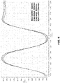
- FIG. 6 is a plot showing a single pulse of a differential output voltage of the example circuit 300 of FIG. 3 , illustrating the transient response when the variable resistors are set at different resistance values. As can be seen from the plot, the higher the resistance value the greater the high frequency boost (although this may cause a longer settling time, which may result in intersymbol interference). The rise time is also shorter for higher resistance values.
- FIG. 7 is a plot showing the rise time of a single pulse of a differential output voltage in the example circuit 300 of FIG. 3 , when the variable resistors 324 are set at different resistance values.
- the rise time may be reduced by up to about 2.2 ps compared to when no high frequency boost is provided.
- the addition of the high frequency booster may enable quicker output response, which may be useful for high speed signaling.
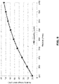
- FIG. 8 is a plot showing the peaking voltage of a single pulse of a 1V differential output voltage in the example circuit 300 of FIG. 3 , when the variable resistors 324 are set at different resistance values. As illustrated in FIG. 8 , by varying the resistance value of the variable resistors 324 from about 200 ohms to about 1000 ohms, the peaking voltage can be controlled to vary between about 10 mV to about 75 mV.
- a transmitter driver circuit in which the output voltage swing is boosted.
- a high frequency booster is added to the conventional transmitter driver circuit to help improve rise/fall time and help provide a high frequency boost.
- the use of variable resistors enables control of the frequency range at which high frequency boost is provided.
- the variable resistors also enable control of rise time and settling time.
- fixed resistors may be used instead of variable resistors (e.g., where the ability to dynamically tune the peaking frequency is not needed).
- control switches may be added to enable the DC voltage boost and high frequency voltage boost to be independently enabled or disabled.
- the examples described herein may provide greater voltage boost at high frequencies (e.g., greater than 56 Gbps). Further, the example circuits described herein may enable voltage boost with a smaller overhead and overall smaller size requirements.
- the present disclosure may also be adapted for single-ended transmitters (e.g., using only high frequency booster with only one feedforward capacitor and one variable resistor).
- Various examples described herein may be used to implement PAM4 signaling in various high speed communication systems, including network, storage, computing and mobile systems.
- the examples described herein may be applicable to standards for high speed communication, for both electrical and optical produces.
Landscapes
- Engineering & Computer Science (AREA)
- Computer Networks & Wireless Communication (AREA)
- Signal Processing (AREA)
- Power Engineering (AREA)
- Dc Digital Transmission (AREA)
- Transmitters (AREA)
Claims (15)
- Sendertreiber (300), der Folgendes umfasst:einen ersten Spannungsmodustreiber (302), der so gekoppelt ist, dass er ein erstes Differenzeingangssignal von einem ersten Eingangsanschluss (D0) des Sendertreibers (300) empfängt, und so gekoppelt ist, dass er ein erstes Differenzausgangssignal an einem ersten Ausgangsanschluss (Tx_m) des Sendertreibers (300) bereitstellt;einen zweiten Spannungsmodustreiber (304), der so gekoppelt ist, dass er ein zweites Differenzeingangssignal von einem zweiten Eingangsanschluss (DOb) des Sendertreibers (300) empfängt, und so gekoppelt ist, dass er ein zweites Differenzausgangssignal an einem zweiten Ausgangsanschluss (Tx_p) des Sendertreibers (300) bereitstellt;einen sekundären Datenpfad (306) mit ersten Eingangs- und Ausgangsanschlüssen, die parallel zu dem ersten Spannungsmodustreiber (302) geschaltet sind, und mit zweiten Eingangs- und Ausgangsanschlüssen, die parallel zu dem zweiten Spannungsmodustreiber (304) geschaltet sind, wobei der sekundäre Datenpfad (306) einen Verstärkungsstrom von einer Stromquelle (326) empfängt;wobei der Sendertreiber dadurch gekennzeichnet ist, dass er ferner Folgendes umfasst:
einen Hochfrequenzverstärker (320), der mit den ersten und zweiten Eingangsanschlüssen des Sendertreibers (300) verbunden und zwischen der Stromquelle (326) und dem sekundären Datenpfad (306) angeschlossen ist, wobei der Hochfrequenzverstärker (320) einen Hochfrequenzpfad für den Verstärkungsstrom von der Stromquelle (326) bereitstellt. - Sendertreiber (300) nach Anspruch 1, wobei der Hochfrequenzverstärker (320) Folgendes umfasst:
ein jeweiliges RC-Netzwerk, das mit jedem der ersten und zweiten Eingangsanschlüsse des Sendertreibers verbunden ist, um den Hochfrequenzpfad bereitzustellen, wobei jedes des jeweiligen RC-Netzwerks, das mit jedem der ersten und zweiten Eingangsanschlüsse des Sendertreibers verbunden ist, einen Vorwärtskopplungskondensator (322) und einen Widerstand (324) aufweist. - Sendertreiber (300) nach Anspruch 2, wobei der Widerstand (324) jedes des jeweiligen RC-Netzwerks, das mit jedem der ersten und zweiten Eingangsanschlüsse des Sendertreibers (300) verbunden ist, ein Regelwiderstand ist.
- Sendertreiber (300) nach Anspruch 3, wobei der Widerstand jedes Regelwiderstands (324) des jeweiligen RC-Netzwerks, das mit jedem der ersten und zweiten Eingangsanschlüsse des Sendertreibers (300) verbunden ist, im Bereich von etwa 0 Ohm bis etwa 1000 Ohm steuerbar variabel ist.
- Sendertreiber (300) nach einem der Ansprüche 2 bis 4, wobei die Kapazität jedes der Vorwärtskopplungskondensatoren (322) des jeweiligen RC-Netzwerks, das mit jedem der ersten und zweiten Eingangsanschlüsse des Sendertreibers (300) verbunden ist, im Bereich von etwa 10 Femtofarad (fF) bis etwa 100 fF liegt.
- Sendertreiber (300) nach einem der Ansprüche 2 bis 5, wobei jeder der Vorwärtskopplungskondensatoren (322) des jeweiligen RC-Netzwerks, das mit jedem der ersten und zweiten Eingangsanschlüsse des Sendertreibers (300) verbunden ist, ein Drehkondensator ist.
- Sendertreiber (400) nach einem der Ansprüche 1 bis 6, der ferner Folgendes umfasst:
einen ersten Satz von Steuerschaltern (402), die mit dem Hochfrequenzverstärker (320) verbunden sind, um den Hochfrequenzpfad zu aktivieren oder zu deaktivieren. - Sendertreiber nach Anspruch 7, der ferner Folgendes umfasst:
einen zweiten Satz von Steuerschaltern (404), die mit dem sekundären Datenpfad (306) verbunden sind, um den Empfang des Verstärkungsstroms zu aktivieren oder zu deaktivieren. - Sender zum Übertragen von Differenzsignalen, der Folgendes umfasst:
einen Sendertreiber (300), der Folgendes umfasst:einen ersten Spannungsmodustreiber (302), der so gekoppelt ist, dass er ein erstes Differenzeingangssignal von einem ersten Eingangsanschluss (D0) des Sendertreibers (300) empfängt, und so gekoppelt ist, dass er ein erstes Differenzausgangssignal an einem ersten Ausgangsanschluss (Tx_m) des Sendertreibers (300) bereitstellt;einen zweiten Spannungsmodustreiber (304), der so gekoppelt ist, dass er ein zweites Differenzeingangssignal von einem zweiten Eingangsanschluss (DOb) des Sendertreibers (300) empfängt, und so gekoppelt ist, dass er ein zweites Differenzausgangssignal an einem zweiten Ausgangsanschluss (Tx_p) des Sendertreibers bereitstellt;einen sekundären Datenpfad (306) mit ersten Eingangs- und Ausgangsanschlüssen, die parallel zu dem ersten Spannungsmodustreiber (302) geschaltet sind, und mit zweiten Eingangs- und Ausgangsanschlüssen, die parallel zu dem zweiten Spannungsmodustreiber (304) geschaltet sind, wobei der sekundäre Datenpfad (306) einen Verstärkungsstrom von einer Stromquelle (326) empfängt;wobei der Sendertreiber dadurch gekennzeichnet ist, dass er ferner Folgendes umfasst:einen Hochfrequenzverstärker (320), der mit den ersten und zweiten Eingangsanschlüssen des Sendertreibers (300) verbunden und zwischen der Stromquelle (326) und dem sekundären Datenpfad (306) angeschlossen ist, wobei der Hochfrequenzverstärker (320) einen Hochfrequenzpfad für den Verstärkungsstrom von der Stromquelle (326) bereitstellt; undeinen mit dem Sendertreiber (300) gekoppelten Prozessor zur Steuerung des Betriebs des Sendertreibers (300). - Sender nach Anspruch 9, wobei der Hochfrequenzverstärker (320) Folgendes umfasst:
ein jeweiliges RC-Netzwerk, das mit jedem der ersten und zweiten Eingangsanschlüsse des Sendertreibers verbunden ist, um den Hochfrequenzpfad bereitzustellen, wobei jedes des jeweiligen RC-Netzwerks, das mit jedem der ersten und zweiten Eingangsanschlüsse des Sendertreibers verbunden ist, einen Vorwärtskopplungskondensator (322) und einen Widerstand (324) aufweist. - Sender nach Anspruch 10, wobei der Widerstand (324) jedes jeweiligen RC-Netzwerks, das mit jedem der ersten und zweiten Eingangsanschlüsse des Sendertreibers verbunden ist, ein Regelwiderstand ist, und wobei der Prozessor so gekoppelt ist, dass er den Widerstand jedes Regelwiderstands steuert.
- Sender nach Anspruch 11, wobei der Widerstand jedes Regelwiderstands (324) des jeweiligen RC-Netzwerks, das mit jedem der ersten und zweiten Eingangsanschlüsse des Sendertreibers (300) verbunden ist, im Bereich von etwa 0 Ohm bis etwa 1000 Ohm steuerbar variabel ist.
- Sender nach einem der Ansprüche 10 bis 12, wobei die Kapazität jedes der Vorwärtskopplungskondensatoren (322) des jeweiligen RC-Netzwerks, das mit jedem der ersten und zweiten Eingangsanschlüsse des Sendertreibers (300) verbunden ist, im Bereich von etwa 10 Femtofarad (fF) bis etwa 100 fF liegt.
- Sender nach einem der Ansprüche 10 bis 13, wobei jeder der Vorwärtskopplungskondensatoren (322) des jeweiligen RC-Netzwerks, das mit jedem der ersten und zweiten Eingangsanschlüsse des Sendertreibers (300) verbunden ist, ein Drehkondensator ist, und wobei der Prozessor gekoppelt ist, um die Kapazität jedes Drehkondensators zu steuern.
- Sender nach einem der Ansprüche 9 bis 14, der ferner Folgendes umfasst:einen ersten Satz von Steuerschaltern (402), die mit dem Hochfrequenzverstärker verbunden sind, um den Hochfrequenzpfad zu aktivieren oder zu deaktivieren;wobei der Prozessor so gekoppelt ist, dass er den ersten Satz von Steuerschaltern ein-oder ausschaltet.
Applications Claiming Priority (2)
| Application Number | Priority Date | Filing Date | Title |
|---|---|---|---|
| US15/425,262 US10044377B1 (en) | 2017-02-06 | 2017-02-06 | High swing transmitter driver with voltage boost |
| PCT/CN2018/075283 WO2018141290A1 (en) | 2017-02-06 | 2018-02-05 | High swing transmitter driver with voltage boost |
Publications (3)
| Publication Number | Publication Date |
|---|---|
| EP3571817A1 EP3571817A1 (de) | 2019-11-27 |
| EP3571817A4 EP3571817A4 (de) | 2020-01-01 |
| EP3571817B1 true EP3571817B1 (de) | 2022-04-06 |
Family
ID=63014014
Family Applications (1)
| Application Number | Title | Priority Date | Filing Date |
|---|---|---|---|
| EP18747203.0A Active EP3571817B1 (de) | 2017-02-06 | 2018-02-05 | Treiber für hochschwingenden sender mit spannungsverstärker |
Country Status (4)
| Country | Link |
|---|---|
| US (1) | US10044377B1 (de) |
| EP (1) | EP3571817B1 (de) |
| CN (1) | CN110301122B (de) |
| WO (1) | WO2018141290A1 (de) |
Families Citing this family (4)
| Publication number | Priority date | Publication date | Assignee | Title |
|---|---|---|---|---|
| EP3373526B1 (de) * | 2017-03-07 | 2020-01-08 | Nxp B.V. | Sender mit unabhängig einstellbarer spannung und impedanz |
| US10469070B1 (en) * | 2017-09-15 | 2019-11-05 | Marvell International Ltd. | PAM-4 voltage-mode driver with stabilized output |
| CN113014243B (zh) * | 2019-12-19 | 2022-11-29 | 上海交通大学 | Pam4模式下高速sst驱动器电平不匹配比优化实现方法 |
| US11431530B2 (en) * | 2020-09-02 | 2022-08-30 | Huawei Technologies Co., Ltd. | Selectable mode transmitter driver |
Family Cites Families (39)
| Publication number | Priority date | Publication date | Assignee | Title |
|---|---|---|---|---|
| US6351185B1 (en) * | 1999-08-16 | 2002-02-26 | Globespan, Inc. | Increased output swing line drivers for operation at supply voltages that exceed the breakdown voltage of the integrated circuit technology |
| JP2002050181A (ja) * | 2000-02-07 | 2002-02-15 | Toshiba Corp | 半導体記憶装置 |
| US6429987B1 (en) * | 2000-04-10 | 2002-08-06 | Marvell International, Inc. | High speed inductor current driver with minimum overshoot |
| WO2003079623A1 (en) * | 2002-03-15 | 2003-09-25 | Gennum Corporation | System and method for compensating line losses over a digital visual interface (dvi) link |
| US7292629B2 (en) * | 2002-07-12 | 2007-11-06 | Rambus Inc. | Selectable-tap equalizer |
| US7532048B1 (en) * | 2004-11-18 | 2009-05-12 | Aquantia Corporation | Multi-level variable-resistor line driver |
| JP2010516104A (ja) * | 2007-01-09 | 2010-05-13 | ラムバス・インコーポレーテッド | 等化送信機および動作方法 |
| US7746591B2 (en) * | 2007-12-14 | 2010-06-29 | Texas Instruments Incorporated | Methods and apparatus to provide dynamically-biased write drivers for hard disk drive (HDD) application |
| JP5114293B2 (ja) * | 2008-05-30 | 2013-01-09 | 株式会社日立製作所 | 波形等化回路 |
| CN102204401A (zh) * | 2008-09-05 | 2011-09-28 | 艾色拉加拿大有限公司 | 具有针对无线应用的可切换输出的无源发射机架构 |
| US7964992B2 (en) * | 2008-09-15 | 2011-06-21 | Silicon Laboratories Inc. | Circuit device including multiple parameterized power regulators |
| US8106684B2 (en) * | 2008-09-24 | 2012-01-31 | Sony Corporation | High-speed low-voltage differential signaling system |
| JPWO2011045832A1 (ja) * | 2009-10-14 | 2013-03-04 | 株式会社アドバンテスト | 差動ドライバ回路およびそれを用いた試験装置 |
| JP2011128440A (ja) * | 2009-12-18 | 2011-06-30 | Fujitsu Ltd | 電圧供給回路及び表示装置 |
| US9008597B2 (en) * | 2010-04-20 | 2015-04-14 | Rf Micro Devices, Inc. | Direct current (DC)-DC converter having a multi-stage output filter |
| WO2011162104A1 (en) * | 2010-06-25 | 2011-12-29 | Semiconductor Energy Laboratory Co., Ltd. | Semiconductor device and method for driving the same |
| TWI491180B (zh) * | 2010-09-08 | 2015-07-01 | Mstar Semiconductor Inc | 具高輸出電壓的低電壓傳輸裝置 |
| US8786321B2 (en) * | 2010-12-30 | 2014-07-22 | Stmicroelectronics International N.V. | Power harvesting in open drain transmitters |
| US8634230B2 (en) * | 2011-01-28 | 2014-01-21 | Semiconductor Energy Laboratory Co., Ltd. | Semiconductor device and method for driving the same |
| US8710752B2 (en) * | 2011-03-03 | 2014-04-29 | Dialog Semiconductor Inc. | Adaptive switch mode LED system |
| US8604876B2 (en) * | 2011-05-13 | 2013-12-10 | Qualcomm, Incorporated | Current buffer |
| US8823421B2 (en) * | 2011-06-30 | 2014-09-02 | Stmicroelectronics International N.V. | Pre-emphasis circuit |
| US8638150B2 (en) | 2011-12-20 | 2014-01-28 | Intersil Americas LLC | Method and system for compensating mode conversion over a communications channel |
| US8797776B2 (en) * | 2012-10-16 | 2014-08-05 | Hong Kong Applied Science & Technology Research Institute Co., Ltd. | Diode-less full-wave rectifier for low-power on-chip AC-DC conversion |
| US9300331B2 (en) * | 2012-11-09 | 2016-03-29 | Omnivision Technologies, Inc. | Method, apparatus and system for providing pre-emphasis in a signal |
| US9710411B2 (en) * | 2013-01-24 | 2017-07-18 | Texas Instruments Incorporated | Signal conditioner |
| JP2014154847A (ja) * | 2013-02-13 | 2014-08-25 | Toshiba Corp | 半導体回路、da変換器、ミキサ回路、無線通信装置、閾値電圧調整方法及びトランジスタの良否判定方法 |
| US8884548B2 (en) * | 2013-02-28 | 2014-11-11 | Asahi Kasei Microdevices Corporation | Power factor correction converter with current regulated output |
| WO2014140660A1 (en) * | 2013-03-14 | 2014-09-18 | Silicon Image, Inc. | Driving data of multiple protocols through a single set of pins |
| JP5990134B2 (ja) * | 2013-06-11 | 2016-09-07 | 株式会社ジャパンディスプレイ | タッチ検出機能付き表示装置及び電子機器 |
| US9871539B2 (en) * | 2013-07-16 | 2018-01-16 | Mediatek Inc. | Driver circuit for signal transmission and control method of driver circuit |
| JP6129677B2 (ja) * | 2013-08-05 | 2017-05-17 | 日立オートモティブシステムズ株式会社 | 電動モータの駆動制御装置 |
| US9153312B2 (en) | 2013-08-23 | 2015-10-06 | Micron Technology, Inc. | Methods and apparatuses including transmitter circuits |
| JP2015198371A (ja) * | 2014-04-01 | 2015-11-09 | ローム株式会社 | オーディオ出力回路およびそれを用いた電子機器 |
| US9679509B2 (en) | 2014-05-01 | 2017-06-13 | Samsung Display Co., Ltd. | Positive feedback enhanced switching equalizer with output pole tuning |
| US9497049B2 (en) | 2014-09-04 | 2016-11-15 | Qualcomm Incorporated | Wideband transmitter with high-frequency signal peaking |
| US9608845B2 (en) * | 2015-02-27 | 2017-03-28 | Huawei Technologies Co., Ltd. | Transmit apparatus and method |
| JP6397811B2 (ja) * | 2015-12-18 | 2018-09-26 | 株式会社東芝 | 半導体集積回路及び高周波アンテナスイッチ |
| US10038382B2 (en) * | 2016-01-19 | 2018-07-31 | Intersil Americas LLC | Current mode 3-state buck-boost PWM control architecture |
-
2017
- 2017-02-06 US US15/425,262 patent/US10044377B1/en active Active
-
2018
- 2018-02-05 CN CN201880010548.0A patent/CN110301122B/zh active Active
- 2018-02-05 EP EP18747203.0A patent/EP3571817B1/de active Active
- 2018-02-05 WO PCT/CN2018/075283 patent/WO2018141290A1/en not_active Ceased
Also Published As
| Publication number | Publication date |
|---|---|
| EP3571817A4 (de) | 2020-01-01 |
| US10044377B1 (en) | 2018-08-07 |
| CN110301122B (zh) | 2020-12-08 |
| CN110301122A (zh) | 2019-10-01 |
| EP3571817A1 (de) | 2019-11-27 |
| WO2018141290A1 (en) | 2018-08-09 |
| US20180227001A1 (en) | 2018-08-09 |
Similar Documents
| Publication | Publication Date | Title |
|---|---|---|
| US10033412B2 (en) | Impedance and swing control for voltage-mode driver | |
| US7696787B2 (en) | Signal history controlled slew-rate transmission method and bus interface transmitter | |
| US8520348B2 (en) | High-swing differential driver using low-voltage transistors | |
| US7830167B2 (en) | Pre-emphasis circuit | |
| US6794900B2 (en) | Method and circuit for pre-emphasis equalization in high speed data communications | |
| US6624670B2 (en) | High speed voltage mode differential digital output driver with edge-emphasis and pre-equalization | |
| US10880133B2 (en) | Voltage-mode transmitter driver | |
| US10313165B2 (en) | Finite impulse response analog receive filter with amplifier-based delay chain | |
| CN117997680A (zh) | 收发器中隔离接收器和发射器的方法和装置 | |
| US8587339B2 (en) | Multi-mode driver with multiple transmitter types and method therefor | |
| US10044377B1 (en) | High swing transmitter driver with voltage boost | |
| KR20150126557A (ko) | 데이터 전송 채널을 이퀄라이징하기 위한 시스템 및 이를 포함하는 디스플레이 | |
| US10659089B2 (en) | Differential data transmitter with pre-emphasis | |
| CA2654553C (en) | Tri-stated driver for bandwidth-limited load | |
| US11431530B2 (en) | Selectable mode transmitter driver | |
| CN110781114A (zh) | 一种高速串行接口接收端的宽带无源线性均衡器电路 | |
| US20050286641A1 (en) | Finite impulse response de-emphasis with inductive shunt peaking for near-end and far-end signal integrity | |
| US11394376B2 (en) | Crosstalk cancellation circuit, transmitter, and transmission and reception system | |
| KR102823144B1 (ko) | Pam-3 신호처리용 미들전압 터미네이션 기반 드라이버 장치 | |
| US20260058849A1 (en) | Continuous time linear equalizer employing current-reuse and current-stealing architecture | |
| CN119449052B (zh) | 发射机均衡驱动电路及待发射信号的处理方法 | |
| EP3635861B1 (de) | Continuous-time-verstärker mit drei eingangssignalen und entzerrer für mehrstufige signalisierung | |
| KR20260065302A (ko) | 저전압 송신 장치 |
Legal Events
| Date | Code | Title | Description |
|---|---|---|---|
| STAA | Information on the status of an ep patent application or granted ep patent |
Free format text: STATUS: THE INTERNATIONAL PUBLICATION HAS BEEN MADE |
|
| PUAI | Public reference made under article 153(3) epc to a published international application that has entered the european phase |
Free format text: ORIGINAL CODE: 0009012 |
|
| STAA | Information on the status of an ep patent application or granted ep patent |
Free format text: STATUS: REQUEST FOR EXAMINATION WAS MADE |
|
| 17P | Request for examination filed |
Effective date: 20190819 |
|
| AK | Designated contracting states |
Kind code of ref document: A1 Designated state(s): AL AT BE BG CH CY CZ DE DK EE ES FI FR GB GR HR HU IE IS IT LI LT LU LV MC MK MT NL NO PL PT RO RS SE SI SK SM TR |
|
| AX | Request for extension of the european patent |
Extension state: BA ME |
|
| A4 | Supplementary search report drawn up and despatched |
Effective date: 20191128 |
|
| RIC1 | Information provided on ipc code assigned before grant |
Ipc: H04L 27/01 20060101AFI20191122BHEP |
|
| DAV | Request for validation of the european patent (deleted) | ||
| DAX | Request for extension of the european patent (deleted) | ||
| GRAP | Despatch of communication of intention to grant a patent |
Free format text: ORIGINAL CODE: EPIDOSNIGR1 |
|
| STAA | Information on the status of an ep patent application or granted ep patent |
Free format text: STATUS: GRANT OF PATENT IS INTENDED |
|
| INTG | Intention to grant announced |
Effective date: 20211019 |
|
| GRAS | Grant fee paid |
Free format text: ORIGINAL CODE: EPIDOSNIGR3 |
|
| GRAA | (expected) grant |
Free format text: ORIGINAL CODE: 0009210 |
|
| STAA | Information on the status of an ep patent application or granted ep patent |
Free format text: STATUS: THE PATENT HAS BEEN GRANTED |
|
| AK | Designated contracting states |
Kind code of ref document: B1 Designated state(s): AL AT BE BG CH CY CZ DE DK EE ES FI FR GB GR HR HU IE IS IT LI LT LU LV MC MK MT NL NO PL PT RO RS SE SI SK SM TR |
|
| REG | Reference to a national code |
Ref country code: GB Ref legal event code: FG4D |
|
| REG | Reference to a national code |
Ref country code: CH Ref legal event code: EP |
|
| REG | Reference to a national code |
Ref country code: AT Ref legal event code: REF Ref document number: 1482431 Country of ref document: AT Kind code of ref document: T Effective date: 20220415 |
|
| REG | Reference to a national code |
Ref country code: IE Ref legal event code: FG4D |
|
| REG | Reference to a national code |
Ref country code: DE Ref legal event code: R096 Ref document number: 602018033401 Country of ref document: DE |
|
| REG | Reference to a national code |
Ref country code: LT Ref legal event code: MG9D |
|
| REG | Reference to a national code |
Ref country code: NL Ref legal event code: MP Effective date: 20220406 |
|
| REG | Reference to a national code |
Ref country code: AT Ref legal event code: MK05 Ref document number: 1482431 Country of ref document: AT Kind code of ref document: T Effective date: 20220406 |
|
| PG25 | Lapsed in a contracting state [announced via postgrant information from national office to epo] |
Ref country code: NL Free format text: LAPSE BECAUSE OF FAILURE TO SUBMIT A TRANSLATION OF THE DESCRIPTION OR TO PAY THE FEE WITHIN THE PRESCRIBED TIME-LIMIT Effective date: 20220406 |
|
| PG25 | Lapsed in a contracting state [announced via postgrant information from national office to epo] |
Ref country code: SE Free format text: LAPSE BECAUSE OF FAILURE TO SUBMIT A TRANSLATION OF THE DESCRIPTION OR TO PAY THE FEE WITHIN THE PRESCRIBED TIME-LIMIT Effective date: 20220406 Ref country code: PT Free format text: LAPSE BECAUSE OF FAILURE TO SUBMIT A TRANSLATION OF THE DESCRIPTION OR TO PAY THE FEE WITHIN THE PRESCRIBED TIME-LIMIT Effective date: 20220808 Ref country code: NO Free format text: LAPSE BECAUSE OF FAILURE TO SUBMIT A TRANSLATION OF THE DESCRIPTION OR TO PAY THE FEE WITHIN THE PRESCRIBED TIME-LIMIT Effective date: 20220706 Ref country code: LT Free format text: LAPSE BECAUSE OF FAILURE TO SUBMIT A TRANSLATION OF THE DESCRIPTION OR TO PAY THE FEE WITHIN THE PRESCRIBED TIME-LIMIT Effective date: 20220406 Ref country code: HR Free format text: LAPSE BECAUSE OF FAILURE TO SUBMIT A TRANSLATION OF THE DESCRIPTION OR TO PAY THE FEE WITHIN THE PRESCRIBED TIME-LIMIT Effective date: 20220406 Ref country code: GR Free format text: LAPSE BECAUSE OF FAILURE TO SUBMIT A TRANSLATION OF THE DESCRIPTION OR TO PAY THE FEE WITHIN THE PRESCRIBED TIME-LIMIT Effective date: 20220707 Ref country code: FI Free format text: LAPSE BECAUSE OF FAILURE TO SUBMIT A TRANSLATION OF THE DESCRIPTION OR TO PAY THE FEE WITHIN THE PRESCRIBED TIME-LIMIT Effective date: 20220406 Ref country code: ES Free format text: LAPSE BECAUSE OF FAILURE TO SUBMIT A TRANSLATION OF THE DESCRIPTION OR TO PAY THE FEE WITHIN THE PRESCRIBED TIME-LIMIT Effective date: 20220406 Ref country code: BG Free format text: LAPSE BECAUSE OF FAILURE TO SUBMIT A TRANSLATION OF THE DESCRIPTION OR TO PAY THE FEE WITHIN THE PRESCRIBED TIME-LIMIT Effective date: 20220706 Ref country code: AT Free format text: LAPSE BECAUSE OF FAILURE TO SUBMIT A TRANSLATION OF THE DESCRIPTION OR TO PAY THE FEE WITHIN THE PRESCRIBED TIME-LIMIT Effective date: 20220406 |
|
| PG25 | Lapsed in a contracting state [announced via postgrant information from national office to epo] |
Ref country code: RS Free format text: LAPSE BECAUSE OF FAILURE TO SUBMIT A TRANSLATION OF THE DESCRIPTION OR TO PAY THE FEE WITHIN THE PRESCRIBED TIME-LIMIT Effective date: 20220406 Ref country code: PL Free format text: LAPSE BECAUSE OF FAILURE TO SUBMIT A TRANSLATION OF THE DESCRIPTION OR TO PAY THE FEE WITHIN THE PRESCRIBED TIME-LIMIT Effective date: 20220406 Ref country code: LV Free format text: LAPSE BECAUSE OF FAILURE TO SUBMIT A TRANSLATION OF THE DESCRIPTION OR TO PAY THE FEE WITHIN THE PRESCRIBED TIME-LIMIT Effective date: 20220406 Ref country code: IS Free format text: LAPSE BECAUSE OF FAILURE TO SUBMIT A TRANSLATION OF THE DESCRIPTION OR TO PAY THE FEE WITHIN THE PRESCRIBED TIME-LIMIT Effective date: 20220806 |
|
| REG | Reference to a national code |
Ref country code: DE Ref legal event code: R097 Ref document number: 602018033401 Country of ref document: DE |
|
| PG25 | Lapsed in a contracting state [announced via postgrant information from national office to epo] |
Ref country code: SM Free format text: LAPSE BECAUSE OF FAILURE TO SUBMIT A TRANSLATION OF THE DESCRIPTION OR TO PAY THE FEE WITHIN THE PRESCRIBED TIME-LIMIT Effective date: 20220406 Ref country code: SK Free format text: LAPSE BECAUSE OF FAILURE TO SUBMIT A TRANSLATION OF THE DESCRIPTION OR TO PAY THE FEE WITHIN THE PRESCRIBED TIME-LIMIT Effective date: 20220406 Ref country code: RO Free format text: LAPSE BECAUSE OF FAILURE TO SUBMIT A TRANSLATION OF THE DESCRIPTION OR TO PAY THE FEE WITHIN THE PRESCRIBED TIME-LIMIT Effective date: 20220406 Ref country code: EE Free format text: LAPSE BECAUSE OF FAILURE TO SUBMIT A TRANSLATION OF THE DESCRIPTION OR TO PAY THE FEE WITHIN THE PRESCRIBED TIME-LIMIT Effective date: 20220406 Ref country code: DK Free format text: LAPSE BECAUSE OF FAILURE TO SUBMIT A TRANSLATION OF THE DESCRIPTION OR TO PAY THE FEE WITHIN THE PRESCRIBED TIME-LIMIT Effective date: 20220406 Ref country code: CZ Free format text: LAPSE BECAUSE OF FAILURE TO SUBMIT A TRANSLATION OF THE DESCRIPTION OR TO PAY THE FEE WITHIN THE PRESCRIBED TIME-LIMIT Effective date: 20220406 |
|
| PLBE | No opposition filed within time limit |
Free format text: ORIGINAL CODE: 0009261 |
|
| STAA | Information on the status of an ep patent application or granted ep patent |
Free format text: STATUS: NO OPPOSITION FILED WITHIN TIME LIMIT |
|
| 26N | No opposition filed |
Effective date: 20230110 |
|
| PG25 | Lapsed in a contracting state [announced via postgrant information from national office to epo] |
Ref country code: AL Free format text: LAPSE BECAUSE OF FAILURE TO SUBMIT A TRANSLATION OF THE DESCRIPTION OR TO PAY THE FEE WITHIN THE PRESCRIBED TIME-LIMIT Effective date: 20220406 |
|
| PG25 | Lapsed in a contracting state [announced via postgrant information from national office to epo] |
Ref country code: SI Free format text: LAPSE BECAUSE OF FAILURE TO SUBMIT A TRANSLATION OF THE DESCRIPTION OR TO PAY THE FEE WITHIN THE PRESCRIBED TIME-LIMIT Effective date: 20220406 |
|
| REG | Reference to a national code |
Ref country code: DE Ref legal event code: R119 Ref document number: 602018033401 Country of ref document: DE |
|
| PG25 | Lapsed in a contracting state [announced via postgrant information from national office to epo] |
Ref country code: MC Free format text: LAPSE BECAUSE OF FAILURE TO SUBMIT A TRANSLATION OF THE DESCRIPTION OR TO PAY THE FEE WITHIN THE PRESCRIBED TIME-LIMIT Effective date: 20220406 |
|
| REG | Reference to a national code |
Ref country code: CH Ref legal event code: PL |
|
| REG | Reference to a national code |
Ref country code: BE Ref legal event code: MM Effective date: 20230228 |
|
| PG25 | Lapsed in a contracting state [announced via postgrant information from national office to epo] |
Ref country code: LU Free format text: LAPSE BECAUSE OF NON-PAYMENT OF DUE FEES Effective date: 20230205 Ref country code: LI Free format text: LAPSE BECAUSE OF NON-PAYMENT OF DUE FEES Effective date: 20230228 Ref country code: CH Free format text: LAPSE BECAUSE OF NON-PAYMENT OF DUE FEES Effective date: 20230228 |
|
| REG | Reference to a national code |
Ref country code: IE Ref legal event code: MM4A |
|
| PG25 | Lapsed in a contracting state [announced via postgrant information from national office to epo] |
Ref country code: IT Free format text: LAPSE BECAUSE OF FAILURE TO SUBMIT A TRANSLATION OF THE DESCRIPTION OR TO PAY THE FEE WITHIN THE PRESCRIBED TIME-LIMIT Effective date: 20220406 Ref country code: IE Free format text: LAPSE BECAUSE OF NON-PAYMENT OF DUE FEES Effective date: 20230205 Ref country code: FR Free format text: LAPSE BECAUSE OF NON-PAYMENT OF DUE FEES Effective date: 20230228 Ref country code: DE Free format text: LAPSE BECAUSE OF NON-PAYMENT OF DUE FEES Effective date: 20230901 |
|
| PG25 | Lapsed in a contracting state [announced via postgrant information from national office to epo] |
Ref country code: BE Free format text: LAPSE BECAUSE OF NON-PAYMENT OF DUE FEES Effective date: 20230228 |
|
| P01 | Opt-out of the competence of the unified patent court (upc) registered |
Free format text: CASE NUMBER: UPC_APP_329648/2023 Effective date: 20230524 |
|
| PG25 | Lapsed in a contracting state [announced via postgrant information from national office to epo] |
Ref country code: BG Free format text: LAPSE BECAUSE OF FAILURE TO SUBMIT A TRANSLATION OF THE DESCRIPTION OR TO PAY THE FEE WITHIN THE PRESCRIBED TIME-LIMIT Effective date: 20220406 |
|
| PG25 | Lapsed in a contracting state [announced via postgrant information from national office to epo] |
Ref country code: BG Free format text: LAPSE BECAUSE OF FAILURE TO SUBMIT A TRANSLATION OF THE DESCRIPTION OR TO PAY THE FEE WITHIN THE PRESCRIBED TIME-LIMIT Effective date: 20220406 |
|
| PG25 | Lapsed in a contracting state [announced via postgrant information from national office to epo] |
Ref country code: CY Free format text: LAPSE BECAUSE OF FAILURE TO SUBMIT A TRANSLATION OF THE DESCRIPTION OR TO PAY THE FEE WITHIN THE PRESCRIBED TIME-LIMIT; INVALID AB INITIO Effective date: 20180205 |
|
| PG25 | Lapsed in a contracting state [announced via postgrant information from national office to epo] |
Ref country code: HU Free format text: LAPSE BECAUSE OF FAILURE TO SUBMIT A TRANSLATION OF THE DESCRIPTION OR TO PAY THE FEE WITHIN THE PRESCRIBED TIME-LIMIT; INVALID AB INITIO Effective date: 20180205 |
|
| PG25 | Lapsed in a contracting state [announced via postgrant information from national office to epo] |
Ref country code: TR Free format text: LAPSE BECAUSE OF FAILURE TO SUBMIT A TRANSLATION OF THE DESCRIPTION OR TO PAY THE FEE WITHIN THE PRESCRIBED TIME-LIMIT Effective date: 20220406 |
|
| PGFP | Annual fee paid to national office [announced via postgrant information from national office to epo] |
Ref country code: GB Payment date: 20260106 Year of fee payment: 9 |