EP3565383A1 - Procédé d'éclairage et dispositif électroluminescent - Google Patents
Procédé d'éclairage et dispositif électroluminescent Download PDFInfo
- Publication number
- EP3565383A1 EP3565383A1 EP19180488.9A EP19180488A EP3565383A1 EP 3565383 A1 EP3565383 A1 EP 3565383A1 EP 19180488 A EP19180488 A EP 19180488A EP 3565383 A1 EP3565383 A1 EP 3565383A1
- Authority
- EP
- European Patent Office
- Prior art keywords
- light
- emitting device
- emitting element
- illumination
- favorably
- Prior art date
- Legal status (The legal status is an assumption and is not a legal conclusion. Google has not performed a legal analysis and makes no representation as to the accuracy of the status listed.)
- Pending
Links
Images


Classifications
-
- C—CHEMISTRY; METALLURGY
- C09—DYES; PAINTS; POLISHES; NATURAL RESINS; ADHESIVES; COMPOSITIONS NOT OTHERWISE PROVIDED FOR; APPLICATIONS OF MATERIALS NOT OTHERWISE PROVIDED FOR
- C09K—MATERIALS FOR MISCELLANEOUS APPLICATIONS, NOT PROVIDED FOR ELSEWHERE
- C09K11/00—Luminescent, e.g. electroluminescent, chemiluminescent materials
- C09K11/08—Luminescent, e.g. electroluminescent, chemiluminescent materials containing inorganic luminescent materials
-
- H—ELECTRICITY
- H01—ELECTRIC ELEMENTS
- H01L—SEMICONDUCTOR DEVICES NOT COVERED BY CLASS H10
- H01L33/00—Semiconductor devices with at least one potential-jump barrier or surface barrier specially adapted for light emission; Processes or apparatus specially adapted for the manufacture or treatment thereof or of parts thereof; Details thereof
- H01L33/02—Semiconductor devices with at least one potential-jump barrier or surface barrier specially adapted for light emission; Processes or apparatus specially adapted for the manufacture or treatment thereof or of parts thereof; Details thereof characterised by the semiconductor bodies
- H01L33/26—Materials of the light emitting region
- H01L33/30—Materials of the light emitting region containing only elements of group III and group V of the periodic system
- H01L33/32—Materials of the light emitting region containing only elements of group III and group V of the periodic system containing nitrogen
-
- H—ELECTRICITY
- H01—ELECTRIC ELEMENTS
- H01L—SEMICONDUCTOR DEVICES NOT COVERED BY CLASS H10
- H01L33/00—Semiconductor devices with at least one potential-jump barrier or surface barrier specially adapted for light emission; Processes or apparatus specially adapted for the manufacture or treatment thereof or of parts thereof; Details thereof
- H01L33/48—Semiconductor devices with at least one potential-jump barrier or surface barrier specially adapted for light emission; Processes or apparatus specially adapted for the manufacture or treatment thereof or of parts thereof; Details thereof characterised by the semiconductor body packages
- H01L33/50—Wavelength conversion elements
- H01L33/501—Wavelength conversion elements characterised by the materials, e.g. binder
- H01L33/502—Wavelength conversion materials
- H01L33/504—Elements with two or more wavelength conversion materials
-
- H—ELECTRICITY
- H05—ELECTRIC TECHNIQUES NOT OTHERWISE PROVIDED FOR
- H05B—ELECTRIC HEATING; ELECTRIC LIGHT SOURCES NOT OTHERWISE PROVIDED FOR; CIRCUIT ARRANGEMENTS FOR ELECTRIC LIGHT SOURCES, IN GENERAL
- H05B45/00—Circuit arrangements for operating light-emitting diodes [LED]
- H05B45/20—Controlling the colour of the light
- H05B45/22—Controlling the colour of the light using optical feedback
-
- H—ELECTRICITY
- H05—ELECTRIC TECHNIQUES NOT OTHERWISE PROVIDED FOR
- H05B—ELECTRIC HEATING; ELECTRIC LIGHT SOURCES NOT OTHERWISE PROVIDED FOR; CIRCUIT ARRANGEMENTS FOR ELECTRIC LIGHT SOURCES, IN GENERAL
- H05B45/00—Circuit arrangements for operating light-emitting diodes [LED]
- H05B45/20—Controlling the colour of the light
- H05B45/24—Controlling the colour of the light using electrical feedback from LEDs or from LED modules
-
- H—ELECTRICITY
- H01—ELECTRIC ELEMENTS
- H01L—SEMICONDUCTOR DEVICES NOT COVERED BY CLASS H10
- H01L2924/00—Indexing scheme for arrangements or methods for connecting or disconnecting semiconductor or solid-state bodies as covered by H01L24/00
- H01L2924/0001—Technical content checked by a classifier
- H01L2924/0002—Not covered by any one of groups H01L24/00, H01L24/00 and H01L2224/00
-
- H—ELECTRICITY
- H01—ELECTRIC ELEMENTS
- H01L—SEMICONDUCTOR DEVICES NOT COVERED BY CLASS H10
- H01L33/00—Semiconductor devices with at least one potential-jump barrier or surface barrier specially adapted for light emission; Processes or apparatus specially adapted for the manufacture or treatment thereof or of parts thereof; Details thereof
- H01L33/48—Semiconductor devices with at least one potential-jump barrier or surface barrier specially adapted for light emission; Processes or apparatus specially adapted for the manufacture or treatment thereof or of parts thereof; Details thereof characterised by the semiconductor body packages
- H01L33/50—Wavelength conversion elements
- H01L33/501—Wavelength conversion elements characterised by the materials, e.g. binder
- H01L33/502—Wavelength conversion materials
Definitions
- the present invention relates to an illumination method by which light emitted from a light-emitting device including a semiconductor light-emitting element that is a light-emitting element illuminates an object, and to a light-emitting device including a semiconductor light-emitting element that is a light-emitting element.
- a GaN related blue light-emitting element as an excitation light source of a yellow phosphor and create a so-called pseudo-white light source from a spectrum of the GaN related blue light-emitting element and a spectrum of the yellow phosphor, use the pseudo-white light source as an illumination light source or create a lighting fixture that incorporates the pseudo-white light source or, further, fabricate a lighting system in which a plurality of such fixtures are arranged in a space (refer to Patent Document 1).
- packaged LEDs for example, those that include the GaN related blue light-emitting element, the yellow phosphor, an encapsulant, and the like in a package material
- a source for example, those that include the GaN related blue light-emitting element, the yellow phosphor, an encapsulant, and the like in a package material
- CCT correlated color temperature
- LCD liquid crystal display
- Attempts to address this issue include superimposing a spectrum of a red phosphor or a red semiconductor light-emitting element on a spectrum of a blue light-emitting element and a spectrum of a yellow phosphor in order to improve scores of a color rendering index (CRI) (CIE (13.3)) as established by the International Commission on Illumination (Commission Internationale de l'Eclairage /CIE) .
- CIE color rendering index
- Non-Patent Document 1 describes a red-based illumination light source.
- a color rendering index is an index which indicates how close a color appearance is, when illuminating with light (test light) of a light-emitting device that is an evaluation object, compared to a color appearance when illuminating with a "reference light” that is selected in correspondence with a CCT of the test light.
- a color rendering index is an index indicating fidelity of the light-emitting device that is an evaluation object.
- R a high average color rendering index
- R i high special color rendering index
- the effect of illuminance of an illuminated objectcausing a variation in color appearance is not included in various color rendition metric that are currently in use. It is an everyday experience that a vivid color of a flower seen outdoors where illuminance is normally around 10000 lx or higher becomes dull once the flower is brought indoors where illuminance is around 500 lx as though the flower itself has changed to a different flower with lower chroma, even though the color is fundamentally the same. Generally, saturation regarding the color appearance of an object is dependent on illuminance, and saturation decreases as illuminance decreases even though a spectral power distribution that is being illuminated is unchanged. In other words, color appearance becomes dull. This effect is known as the Hunt effect.
- the Hunt effect is not actively considered for overall evaluation of a light-emitting device such as a light source, a fixture, or a system.
- the simplest way to compensate for the Hunt effect is to dramatically increase indoor illuminance, this causes an unnecessary increase in energy consumption.
- a specific method of achieving a color appearance or an object appearance that is as natural, vivid, highly visible, and comfortable as perceived outdoors under illuminance comparable to an indoor illumination environment remains to be revealed.
- the present invention has been made in order to solve problems such as those described above, and a primary object of the present invention is to provide an illumination method and an overall light-emitting device such as an illumination light source, a lighting fixture, and a lighting system which are capable of achieving, under an indoor illumination environment where illuminance is around 5000 lx or lower including cases where detailed work is performed and generally around 1500 lx or lower, a color appearance or an object appearance as perceived by a person which is as natural, vivid, highly visible, and comfortable as perceived outdoors in a high-illuminance environment regardless of scores of various color rendition metric.
- Another object of the present invention is to achieve a highly efficient and comfortable illuminated environment.
- Yet another object of the present invention is to provide a design guideline for such favorable light-emitting devices.
- An illumination method comprising: illuminated objects preparation step of preparing illuminated objects; and an illumination step of illuminating the objects by light emitted from light-emitting devices including a semiconductor light-emitting element that is a light-emitting element, wherein in the illumination step, when light emitted from the light-emitting devices illuminate the objects, the objects are illuminated so that the light measured at a position of the objects satisfies (1), (2), and (3) below: (1) a distance D uvSSL from a black-body radiation locus as defined by ANSI C78.377 of the light measured at the position of the objects satisfies -0.0350 ⁇ D uvSSL ⁇ -0.0040; (2) if an a* value and a b* value in CIE 1976 L*a*b* color space of 15 Munsell renotation color samples from #01 to #15 listed below when mathematically
- an illumination method and a light-emitting device are achieved which are capable of realizing a truly favorable color appearance of objects statistically judged by a large number of subjects to be more favorable even at an approximately similar CCT and/or an approximately similar illuminance.
- colors among close hues can be identified more easily and work or the like can be performed as comfortably as though under a high-illuminance environment as compared to cases where illumination is performed with experimental reference light or experimental pseudo-reference light even at an approximately similar CCT and/or an approximately similar illuminance.
- a plurality of lipsticks with similar red colors can be more readily distinguished from each other.
- objects can be viewed more clearly and readily as though viewed under a high-illuminance environment as compared to cases where illumination is performed with experimental reference light or experimental pseudo-reference light even at an approximately similar CCT and/or an approximately similar illuminance.
- an illumination method specifies the invention based on light at a position where an object is illuminated in a case where light emitted from a light-emitting device used in the illumination method illuminates the object. Therefore, illumination methods used by light-emitting devices capable of emitting light at a "position where an object is illuminated" which meets requirements of the present invention are to be included in the spirit and scope of the present invention.
- second and third embodiments of the present invention specify the invention based on light in a "main radiant direction" among light emitted from a light-emitting device. Therefore, light-emitting devices capable of radiating light including light in a "main radiant direction" which meets requirements of the present invention are to be included in the spirit and scope of the present invention.
- the "main radiant direction" refers to a direction in which light is radiated over a suitable range and in a suitable orientation which are in line with usage of the light-emitting device.
- the "main radiant direction" may be a direction in which luminous intensity or luminance of the light-emitting device is maximum or locally maximum.
- the "main radiant direction" may be a direction having a finite range including a direction in which the luminous intensity or the luminance of the light-emitting device is maximum or locally maximum.
- the "main radiant direction" may be a direction in which radiant intensity or radiance of the light-emitting device is maximum or locally maximum.
- the "main radiant direction" may be a direction having a finite range including a direction in which the radiant intensity or the radiance of the light-emitting device is maximum or locally maximum.
- a main radiant direction may be a vertical direction of each light-emitting device or within a finite solid angle which includes the vertical direction and which ranges between, for example, a maximum of ⁇ (sr) and a minimum of ⁇ /100 (sr).
- a main radiant direction may be a vertical direction of each light-emitting device or within a finite solid angle which includes the vertical direction and which ranges between, for example, a maximum of ⁇ (sr) and a minimum of ⁇ /100 (sr).
- the main radiant direction may be a direction in which luminous intensity or luminance of the light-emitting device is maximum or locally maximum.
- the main radiant direction may be within a finite solid angle that includes a direction in which luminous intensity or luminance of the light-emitting device is maximum or locally maximum and which ranges between, for example, a maximum of ⁇ (sr) and a minimum of ⁇ /100 (sr).
- the main radiant direction may be a direction in which radiant intensity or radiance of the light-emitting device is maximum or locally maximum.
- the main radiant direction may be within a finite solid angle which includes a direction in which radiant intensity or radiance of the light-emitting device is maximum or locally maximum and which ranges between, for example, a maximum of ⁇ (sr) and a minimum of ⁇ /100 (sr) .
- the main radiant direction may be a vertical direction of a planar center of each light-emitting device or within a finite solid angle which includes the vertical direction and which ranges between, for example, a maximum of ⁇ (sr) and a minimum of ⁇ /100 (sr).
- the main radiant direction may be a direction in which luminous intensity or luminance of the light-emitting device is maximum or locally maximum.
- the main radiant direction may be within a finite solid angle which includes a direction in which luminous intensity or luminance of the light-emitting device is maximum or locally maximum and which ranges between, for example, a maximum of ⁇ (sr) and a minimum of ⁇ /100 (sr).
- the main radiant direction may be a direction in which radiant intensity or radiance of the light-emitting device is maximum or locally maximum.
- the main radiant direction may be within a finite solid angle which includes a direction in which radiant intensity or radiance of the light-emitting device is maximum or locally maximum and which ranges between, for example, a maximum of ⁇ (sr) and a minimum of ⁇ /100 (sr).
- a spectral power distribution of light emitted in the main radiant direction by the light-emitting device is favorably measured at a distance where illuminance at a measuring point is a practical illuminance (as will be described later, 150 lx or higher and 5000 lx or lower).
- reference light as defined by CIE which is used in calculations for estimating a mathematical color appearance may sometimes be referred to as reference light, calculational reference light, and the like.
- experimental reference light which is used when making actual visual comparisons or, in other words, light from an incandescent bulb which incorporates a tungsten filament or the like may sometimes be referred to as reference light, experimental reference light and the like.
- light with a high R a and a high R i which is estimated to have a color appearance that is close to reference light such as light from an LED light source which is used as alternate light for experimental reference light in a visual comparison experiment may sometimes be referred to as reference light, experimental pseudo-reference light and the like.
- light that is an object of a mathematical or experimental examination may sometimes be referred to as test light in contrast to reference light.
- the light-emitting device used in the illumination method according to the first embodiment of the present invention includes a semiconductor light-emitting element that is a light-emitting element.
- the light-emitting device according to the second embodiment of the present invention includes a semiconductor light-emitting element that is a light-emitting element. Configurations other than the above are not particularly limited, and an individual semiconductor light-emitting element to which a lead or the like as a conducting mechanism is added or a packaged LED to which a heat dissipating mechanism is further added and integrated with a phosphor or the like may be adopted.
- an LED module in which a robust heat dissipating mechanism is added to one or more packaged LEDs and which is generally mounted with a plurality of packaged LEDs may be adopted.
- an LED lighting fixture in which a lens, a light-reflecting mechanism, and the like are added to a packaged LED and the like may be adopted.
- a lighting system which supports a large number of LED lighting fixtures or the like and which is configured to be capable of illuminating an object may be adopted.
- the light-emitting device according to the present embodiment encompasses all of the above.
- the present inventor has discovered a radiometric property or a photometric property common to spectra or spectral power distributions capable of realizing a color appearance or an object appearance which is as natural, vivid, highly visible, and comfortable as though perceived outdoors in a high-illuminance environment even in an ordinary indoor illuminance environment.
- the present inventor further ascertained, from a colorimetric perspective, in what way the color appearance of the color samples having specific spectral reflectance characteristics when assuming that the color is illuminated by light having the aforementioned spectrum or spectral power distribution changes (or does not change) when the object described above is achieved in comparison with a case where illumination by calculational reference light is assumed, and collectively reached the present invention. It should be noted that the present invention was made based on experimental facts which defy common and conventional wisdom.
- a baseline mathematical examination was conducted on the assumption of: A) a packaged LED light source incorporating both a semiconductor light-emitting element and a phosphor; and B) a packaged LED light source which does not include a phosphor and which only incorporates a semiconductor light-emitting element as a light-emitting element, which both have a high degree of freedom in setting a spectral power distribution.
- prototypes of a packaged LED light source and a lighting fixture incorporating the packaged LED light source were made based on the mathematically examined test light.
- an incandescent bulb with a tungsten filament was prepared as experimental reference light.
- prototypes of a light source capable of emitting light (experimental pseudo-reference light) with high R a and high R i and which produces a color appearance that is close to that of calculational reference light as well as a lighting fixture incorporating the light source were also made.
- chromatic objects As a third step, comparative visual experiments were performed. Due consideration was given to preparing chromatic objects so that colors of the observation objects covered all hues including purple, bluish purple, blue, greenish blue, green, yellowish green, yellow, reddish yellow, red, and reddish purple. Achromatic objects such as white objects and black objects were also prepared. These chromatic and achromatic objects were prepared in wide varieties and in large numbers including still objects, fresh flowers, food, clothing, and printed material. At this point, the subjects were asked to evaluate a color appearance when the objects were illuminated by experimental reference light or experimental pseudo-reference light and a color appearance when the objects were illuminated by test light. Comparisons between the former and the latter were performed at similar CCTs and similar illuminance. The subjects were asked to perform evaluations from the perspective of which of the lights had relatively achieved a color appearance or an object appearance that is as natural, vivid, highly visible, and comfortable as though perceived outdoors. The subjects were also asked the reasons for their judgment regarding which is superior or inferior.
- radiometric properties and photometric properties of the experimental reference light/experimental pseudo-reference light and the test light were extracted from actual measured values. Furthermore, a difference in colorimetric properties regarding a color appearance of color samples having specific spectral reflectance characteristics which differs from the observation objects described above between a case where illumination at a spectral power distribution of calculational reference light is calculationally assumed and a case where illumination at a spectral power distribution of an actually measured experimental reference light/experimental pseudo-reference light/test light is calculationally assumed was compared with the evaluations by the subjects in the visual experiments, and characteristics of the illumination method or the light-emitting device determined to be truly comfortable were extracted. Moreover, contents of the third and fourth steps also represent examples/comparative examples of the illumination method according to the first embodiment of the present invention, and contents of the second, third, and fourth steps also represent examples/comparative examples of the second and third embodiments of the present invention.
- a spectral power distribution at a position where light emitted from a light-emitting device mainly examined in the illumination method according to the present invention illuminates an object or a spectral power distribution of light in a main radiant direction which is emitted by the light-emitting device according to the present invention was assumed to vary saturation of an illuminated object from a case where illumination is performed using reference light. At this point, the following selections were made in order to quantify a color appearance or a variation thereof.
- a color sample with obvious mathematical spectral reflectance characteristics is favorably defined and a difference in color appearance of the color sample between a case of illumination by calculational reference light and a case of illumination by test light is adopted as an index.
- color samples R 1 to R 8 which are used when deriving an average color rendering index or the like are color samples with intermediate chroma and were therefore considered unsuitable when discussing saturation of high-chroma colors.
- R 9 to R 12 are high-chroma color samples, there are not enough samples for a detailed discussion covering a range of all hue angles.
- selection of a color space and selection of a chromatic adaptation formula are also important when quantitatively evaluating color appearance that is mathematically derived from the spectral power distributions described above.
- CIE 1976 L*a*b* CIELAB
- CMCCAT2000 Cold Measurement Committee's Chromatic Adaptation Transform of 2000
- chromaticity derived from a light source a spectral power distribution at a position where an object is illuminated by light from the light source, or a spectral power distribution of light in a main radiant direction emitted from a light-emitting device can be defined by, for example, a CIE 1931 (x,y) chromaticity diagram
- the derived chromaticity is favorably discussed using a CIE 1976 (u',v') chromaticity diagram which is a more uniform chromaticity diagram.
- a (u' , (2/3)v') chromaticity diagram (synonymous with a CIE 1960 (u,v) chromaticity diagram) is particularly used.
- D uv as described in the present specification is an amount defined by ANSI C78.377 and represents a distance of closest approach to a black-body radiation locus on a (u', (2/3) v') chromaticity diagram as an absolute value thereof.
- a positive sign means that a chromaticity point of a light-emitting device is above (on a side where v' is greater than) the black-body radiation locus
- a negative sign means that the chromaticity point of the light-emitting device is below (on a side where v' is smaller than) the black-body radiation locus.
- the color appearance of an object can vary even if the chromaticity point remains the same.
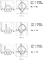
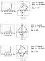
- peak wavelengths of blue semiconductor light-emitting elements were respectively set to 459 nm for FIG. 1 , 475 nm for FIG. 2 , and 425 nm for FIG. 3 .
- Expected color appearances of the 15 color samples when assuming illumination at the respective spectral power distributions and illumination by calculational reference lights corresponding to the respective spectral power distributions are as depicted in the CIELAB color spaces in FIGS. 1 to 3 .
- points connected by dotted lines represent illumination by calculational reference light and points connected by solid lines represent illumination by test light.
- a direction perpendicular to the plane of paper represents lightness, only a* and b* axes were plotted for the sake of convenience.
- the present inventor mathematically examined color appearances of the 15 color samples when assigning different D uv values to a plurality of spectral power distributions while comparing with a case where illumination is performed by calculational reference light.
- white appears greenish when D uv is biased toward positive
- white appears reddish when D uv takes a negative value
- overall color appearance becomes unnatural when D uv deviates from the vicinity of 0.
- coloring of white induces such perceptions.
- the present inventor conducted the following examination with an aim to increase saturation controllability.
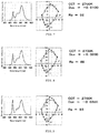
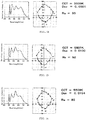
- the eight spectral power distributions shown in FIGS. 4 to 11 represent calculation results of varying D uv from -0.0500 to +0.0150 at a same CCT (2700 K) when assuming a packaged LED which incorporates a blue semiconductor light-emitting element with a peak wavelength of 459 nm and which uses the blue semiconductor light-emitting element as an excitation light source of a green phosphor and a red phosphor.
- Expected color appearances of the 15 color samples when assuming illumination at the respective spectral power distributions (test lights) and illumination by calculational reference lights corresponding to the respective test lights are as represented in the CIELAB color spaces in FIGS. 4 to 11 .
- test lights shown in FIGS. 7 to 11 represent examples where D uv is shifted in a negative direction from -0.0100 to -0.0500.
- D uv is shifted in the negative direction
- the present inventor mathematically examined predictions of color appearances of the 15 most vivid color samples which are positioned outermost in the Munsell renotation color system when assigning various D uv values to test lights in which spectrum-forming light-emitting elements (light-emitting materials) differ from each other while comparing with calculational reference lights.
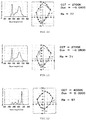
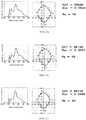
- the 10 spectral power distributions shown in FIGS. 12 to 21 represent results of varying D uv from -0.0500 to +0.0400 at a same CCT (4000 K) when a packaged LED incorporating four semiconductor light-emitting elements is assumed. Peak wavelengths of the four semiconductor light-emitting elements were respectively set to 459 nm, 528 m, 591 nm, and 662 nm. Expected color appearances of the 15 color samples when assuming illumination by the 10 respective test lights and illumination by the calculational reference lights corresponding to the respective test lights are as represented in the CIELAB color spaces in FIGS. 12 to 21 . In the drawings, points connected by dotted lines represent results obtained with the calculational reference lights and points connected by solid lines represent results regarding the respective test lights. Moreover, while a direction perpendicular to the plane of paper represents lightness, only a* and b* axes were plotted for the sake of convenience.
- test lights shown in FIGS. 17 to 21 represent examples where D uv is shifted in a negative direction from -0.0100 to -0.0500.
- D uv is shifted in the negative direction
- the present inventor mathematically examined predictions of color appearances of the 15 most vivid color samples which are positioned outermost in the Munsell renotation color system when assigning various D uv values to test lights in which spectrum-forming light-emitting elements (light-emitting materials) further differ from each other while comparing with calculational reference light.
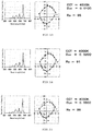
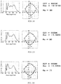
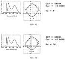
- the 11 spectral power distributions shown in FIGS. 22 to 32 represent calculation results of varying D uv from -0.0448 to +0.0496 at a close CCT (approximately 5500 K) when assuming a packaged LED which incorporates a purple semiconductor light-emitting element and which uses the purple semiconductor light-emitting element as an excitation light source of a blue phosphor, a green phosphor, and a red phosphor.
- a peak wavelength of the incorporated semiconductor light-emitting element was set to 405 nm.
- the result shown in FIG. 32 was obtained without including a green phosphor in order to cause D uv to take an excessively negative value.
- test lights shown in FIGS. 28 to 32 represent examples where D uv is shifted in a negative direction from -0.0100 to -0.0448.
- an a* value and a b* value of the 15 color samples in a CIE 1976 L*a*b* color space of test light as measured at a position of an object when the object is illuminated by the test light (according to the illumination method of the present invention) and test light when a light-emitting device emits the test light in a main radiant direction (according to the light-emitting device of the present invention) be respectively denoted by a* nSSL and b* nSSL (where n is a natural number from 1 to 15), hue angles of the 15 color samples be respectively denoted by ⁇ nSSL (degrees) (where n is a natural number from 1 to 15), an a* value and a b* value of the 15 color samples in a CIE 1976 L*a*b* color space when mathematically assuming illumination by calculational reference light that is selected according to a CCT of the test light (black-body radiator when lower than 5000 K and CIE daylight when equal to
- ⁇ C max a maximum saturation difference value among the 15 Munsell renotation color samples
- ⁇ C min a minimum saturation difference value among the 15 Munsell renotation color samples
- the index A cg is an attempt to describe a difference between a color appearance by experimental reference light or experimental pseudo-reference light and a color appearance by test light as a radiometric property and a photometric property of a spectral power distribution or a spectrum shape.
- the index A cg has been defined in the present invention as follows.
- ⁇ ref ( ⁇ ) and ⁇ SSL ( ⁇ ) respectively denote spectral power distributions of calculational reference light and test light which represent color stimuli that differ from one another when measured at a position of an illuminated objects (according to the illumination method of the present invention) or when measuring light emitted in a main radiant direction from a light-emitting device (according to the light-emitting device of the present invention), x ( ⁇ ), y ( ⁇ ), and z ( ⁇ ) denote a color-matching function, and (X ref , Y ref , Z ref ) and (X SSL , Y SSL , Z SSL ) respectively denote tristimulus values corresponding to the calculational reference light and the test light.
- a cg ⁇ ⁇ 1 ⁇ 2 ⁇ S ⁇ d ⁇ + ⁇ ⁇ 2 ⁇ 3 ⁇ ⁇ S ⁇ d ⁇ + ⁇ ⁇ 3 ⁇ 4 ⁇ S ⁇ d ⁇ Moreover, upper and lower limit wavelengths of the integrals were respectively set to
- ⁇ 4 was defined divided into the following two cases.
- S SSL ( ⁇ ) when a wavelength which provides a longest wavelength local maximum value within 380 nm to 780 nm is denoted by ⁇ R (nm) and a spectral intensity of the wavelength ⁇ R (nm) is denoted by S SSL ( ⁇ R ), a wavelength which is on a longer wavelength-side of ⁇ R and which has an intensity of S SSL ( ⁇ R )/2 was adopted as ⁇ 4. If no such wavelength exists within a range up to 780 nm, then ⁇ 4 was set to 780 nm.
- the index A cg is used when a visible range related to radiations that are color stimuli is roughly divided into a short wavelength range (or the blue region including purple and the like), an intermediate wavelength range (the green region including yellow and the like), and a long wavelength range (the red region including orange and the like) in order to determine whether a concave and/or a convex shapeof a spectrum exist at an appropriate intensity and at an appropriate position in a normalized test light spectral power distribution as compared to a mathematically normalized reference light spectral power distribution.
- long wavelength integral ranges differ according to positions of a longest wavelength local maximum value.
- selections of calculational reference light differ according to a CCT of test light. In the case of FIG.
- a first term of A cg (an integral of ⁇ S ( ⁇ )) is more likely to have a negative value when a spectrum intensity of the normalized test light spectral power distribution is higher than that of the mathematically normalized reference light spectral power distribution.
- a second term of A cg (an integral of - ⁇ S ( ⁇ )) is more likely to have a negative value when a spectrum intensity of the normalized test light spectral power distribution is lower than that of the normalized reference light spectral power distribution.
- a third term of A cg (an integral of ⁇ S ( ⁇ )) is more likely to have a negative value when a spectrum intensity of the normalized test light spectral power distribution is higher than that of the normalized reference light spectral power distribution.
- the calculational reference light varies according to the CCT of the test light.
- black-body radiator is used as the calculational reference light when the CCT of the test light is lower than 5000 K
- defined CIE daylight is used as the calculational reference light when the CCT of the test light is equal to or higher than 5000 K.
- K Km ⁇ ⁇ 380 780 ⁇ SSL ⁇ ⁇ V ⁇ d ⁇ / ⁇ 380 780 ⁇ SSL ⁇ d ⁇
- the luminous efficacy of radiation K (lm/W) of the test light spectral power distribution ⁇ SSL ( ⁇ ) when measured at a position of an illuminated object (according to the illumination method of the present invention) or when measuring light emitted in a main radiant direction from a light-emitting device (according to the light-emitting device of the present invention) is an amount that equals luminous efficacy of a source ⁇ (lm/W) when an efficiency of the spectral power distribution which is attributable to its shape and which is related to characteristics of all materials constituting the light-emitting device (for example, efficiencies such as internal quantum efficiency and light extraction efficiency of a semiconductor light-emitting element, internal quantum efficiency and external quantum efficiency of a phosphor, and light transmission characteristics of an encapsulant) is 100%.
- prototypes of a packaged LED light source and a lighting fixture were made based on the mathematically examined spectra (test lights) .
- prototypes of a light source for light with a high R a and a high R i and which produces a color appearance that is close to that of calculational reference light as well as prototypes of a lighting fixture incorporating the light source were also made.
- prototypes of a light source that excites a green phosphor and a red phosphor using a blue semiconductor light-emitting element, a light source that excites a yellow phosphor and a red phosphor using a blue semiconductor light-emitting element, and a light source that excites a blue phosphor, a green phosphor, and a red phosphor using a purple semiconductor light-emitting element were made and instrumentalized.
- BAM or SBCA was used as the blue phosphor.
- BSS, ⁇ -SiAlON, or BSON was used as the green phosphor.
- YAG was used as the yellow phosphor.
- CASON or SCASN was used as the red phosphor.
- a normally practiced method was used when making packaged LED prototypes. Specifically, a semiconductor light-emitting element (chip) was flip-chip-mounted on a ceramic package which incorporated metal wiring capable of providing electric contact. Next, a slurry created by mixing a phosphor to be used and a binder resin was arranged as a phosphor layer.
- the packaged LEDs were used to create LED bulbs of MR16 Gu10 and MR16 Gu5.3, and the like.
- the LED bulbs were made into a type of a lighting fixture by building a drive circuit into the LED bulbs and also mounting a reflecting mirror, a lens, and the like to the LED bulbs.
- some commercially available LED bulbs were also prepared.
- incandescent bulbs incorporating a tungsten filament were also prepared to be used as experimental reference light.
- a large number of the LED bulbs were arranged to produce a lighting system for conducting comparative visual experiments.
- a system capable of illumination by instantaneously switching among three kinds of bulbs was assembled.
- a type of drive power wire was dedicated for an incandescent bulb having a tungsten filament (experimental reference light), and an adjustable transformer was arranged at a subsequent stage so that the CCT can be varied by boosting drive voltage from 110 V to 130 V relative to 100 V input voltage.
- two remaining lines of the drive power wire were used for the LED bulbs, in which one system was used for experimental pseudo-reference light (LED light source) and the other for test light.
- comparative visual experiment were conducted in which subjects were asked to evaluate color appearances of a large number of observation objects while switching between experimental reference light (or experimental pseudo-reference light) and test light.
- the lighting system was installed in a dark room in order to remove disturbance.
- illuminance at the positions of the observation objects was set approximately the same by varying the number of fixtures of experimental reference light (or experimental pseudo-reference light) and test light which were mounted to the lighting system.
- the experiment was conducted within an illuminance range of approximately 150 lx to approximately 5000 lx.
- Illuminated objects and observed objects which were actually used will be listed below. Due consideration was given to preparing chromatic objects so that colors of all hues including purple, bluish purple, blue, greenish blue, green, yellowish green, yellow, reddish yellow, red, and reddish purple were represented. Achromatic objects such as white objects and black objects were also prepared. Illuminated objects with color were prepared. In addition, these objects were prepared in wide varieties and in large numbers including still objects, fresh flowers, food, clothing, and printed material. Furthermore, the skins of the subjects (Japanese) themselves were also included in the experiment as observation objects. Moreover, the color names partially added to the object names listed below simply signify that such objects will appear in such colors in an ordinary environment and are not accurate representations of the colors.
- the prepared experimental reference light, experimental pseudo-reference light, and test light were divided per CCT as measured at the position of illuminated objects (according to the illumination method of the present invention) or lights emitted in the main radiant directions among the prepared experimental reference light, experimental pseudo-reference light, and test light were divided per CCT (according to the light-emitting device of the present invention) into six experiments. Details are as follows.
- Table 1 CCT classification in visual experiments Experiment CCT range (K) A 2500 or higher lower than 2600 B 2600 or higher lower than 2700 C 2700 or higher lower than 2900 D 2900 or higher lower than 3250 E 3500 or higher lower than 4100 F 5400 or higher lower than 5700
- results of comparative visual experiments conducted in the third step using the prototypes of LED light sources/fixtures/systems made in the second step were compiled.
- Table 2 represents results corresponding to experiment A and Table 3 represents results corresponding to experiment B.
- Table 7 represents results corresponding to experiment F.
- a comparable appearance is represented by a central "0”
- an evaluation that the test light is slightly favorable is represented by "1”
- an evaluation that the test light is favorable is represented by "2”
- an evaluation that the test light is more favorable is represented by "3”
- an evaluation that the test light is extremely favorable is represented by "4"
- an evaluation that the test light is dramatically favorable is represented by "5".
- an evaluation that the test light is slightly unfavorable is represented by "-1"
- an evaluation that the test light is unfavorable is represented by "-2”
- an evaluation that the test light is more unfavorable is represented by "-3”
- an evaluation that the test light is extremely unfavorable is represented by "-4”
- an evaluation that the test light is dramatically unfavorable is represented by "-5”.
- the fourth step in particular, an attempt was made to extract a radiometric property and a photometric property of a spectral power distribution shared by the test light from an actually measured spectrum in a case where the color appearance of an illuminated object when illuminated by the test light was judged to be more favorable than when illuminated by experimental reference light or experimental pseudo-reference light in a visual experiment.
- test lights and comparative test lights in the tables may sometimes be collectively referred to as a "test light".
- Tables 4, 5, and 7 include results in which the D uv of test light is on the positive side of experimental reference light (or experimental pseudo-reference light). From these results, it is found that the greater the positive value of the D uv of the test light, the less favorable the color appearance or the object appearance of the illuminated objects as judged by the subjects. A more specific description will be given below.
- Tables 2 to 7 include results in which the D uv of test light is on the negative side of experimental reference light (or experimental pseudo-reference light) . These results show that when the D uv of the test light was in an appropriate negative range and the various indices in the tables were in appropriate ranges, the subjects judged the color appearance or the object appearance of the illuminated object to be slightly favorable, favorable, more favorable, extremely favorable, or dramatically favorable. On the other hand, it is also shown that even if the D uv of the test light was in a similar range, the color appearance or the object appearance of the illuminated object was judged to be unfavorable when the various indices in the tables were not in appropriate ranges as shown in Table 5.
- legibility had slightly increased, increased, further increased, extremely increased, or dramatically increased in comparison to being illuminated by experimental reference light (or experimental pseudo-reference light) when the D uv of the test light was in an appropriate negative range and the various indices in the tables were in appropriate ranges.
- experimental reference light or experimental pseudo-reference light
- the subjects judged that the color appearances of the illuminated objects had a slightly natural vividness, a natural vividness, a further natural vividness, an extremely natural vividness, or a dramatically natural vividness in comparison to being illuminated by experimental reference light (or experimental pseudo-reference light) when the D uv of the test light was in an appropriate negative range and the various indices in the tables were in appropriate ranges.
- experimental reference light or experimental pseudo-reference light
- the subjects judged that the color appearances of the color samples were slightly close, close, further close, extremely close, or dramatically close to their memories when seeing the color samples outdoors in comparison to being illuminated by experimental reference light (or experimental pseudo-reference light) when the D uv of the test light was in an appropriate negative range and the various indices in the tables were in appropriate ranges.
- the subjects also pointed out that the closer to an optimum range, the more natural and favorable the color appearance, which more closely resembled their memories when seeing the color samples outdoors. This was a totally unexpected result.
- the index A cg and the luminous efficacy of radiation K (lm/W) are favorably within appropriate ranges.
- test lights which produced a favorable color appearance or a favorable object appearance had the following characteristics with respect to the color appearance of the 15 color samples when illumination by calculational reference light is assumed and the color appearance of the 15 color samples when illumination by an actually measured test light spectral power distribution is assumed.
- individual saturations ( ⁇ C n ) of the 15 color samples also show that none of the respective ⁇ C n of the 15 color samples when illuminated by the test lights was excessively lower or higher than the same values when illuminated by the calculational reference light and were all in appropriate ranges.
- a solid line in FIG. 35 represents a normalized test light spectral power distribution of test light 5 judged to be "dramatically favorable" in the comprehensive judgment shown in Table 3.
- a dotted line in FIG. 35 represents a normalized spectral power distribution of calculational reference light (black-body radiator) calculated based on a CCT of the test light.
- FIG. 36 represents a CIELAB plot related to color appearances of the 15 color samples when assuming illumination by the test light 5 (solid line) and assuming illumination by the calculational reference light (black-body radiator) (dotted line).
- a direction perpendicular to the plane of paper represents lightness, only a* and b* axes were plotted for the sake of convenience.
- FIGS. 37 and 38 summarize results of test light 15 judged to be “dramatically favorable” in the comprehensive judgment shown in Table 5 in a similar manner to that described above
- FIGS. 39 and 40 summarize results of test light 19 judged to be “dramatically favorable” in the comprehensive judgment shown in Table 6 in a similar manner to that described above.
- FIGS. 41 and 42 represent a result of a CIELAB plot performed with respect to a normalized spectral power distribution and color appearances of the 15 color samples for the comparative test light 14 in a similar manner to FIGS. 35, 36 , and the like.
- D uv in the illumination method according to the first embodiment of the present invention was -0.0040 or lower, slightly favorably -0.0042 or lower, favorably -0.0070 or lower, more favorably -0.0100 or lower, extremely favorably -0.0120 or lower, and dramatically favorably -0.0160 or lower.
- D uv in the illumination method according to the first embodiment of the present invention was -0.0350 or higher, slightly favorably -0.0340 or higher, favorably -0.0290 or higher, more favorably -0.0250 or higher, extremely favorably -0.0230 or higher, and dramatically favorably -0.0200 or higher.
- in the illumination method according to the first embodiment of the present invention was 9.0 or lower, extremely favorably 8.4 or lower, and dramatically favorably 7.3 or lower.
- is more favorable and that each
- in the illumination method according to the first embodiment of the present invention was 0 or higher and a minimum value thereof during the visual experiments was 0.0029. Furthermore, an examination performed using actual test light during the visual experiments revealed that a favorable range of each
- ⁇ n 1 15 ⁇ C n 15 in the illumination method according to the first embodiment of the present invention was: 1.0 or higher, slightly favorably 1.1 or higher, favorably 1.9 or higher, extremely favorably 2.3 or higher, and dramatically favorably 2.6 or higher; and 7.0 or lower, favorably 6.4 or lower, extremely favorably 5.1 or lower, and dramatically favorably 4.7 or lower.
- Each ⁇ C n in the illumination method according to the first embodiment of the present invention was -3.8 or higher, slightly favorably -3.5 or higher, extremely favorably -2.5 or higher, and dramatically favorably -0.7 or higher.
- each ⁇ C n in the illumination method according to the first embodiment of the present invention was 18.6 or lower, extremely favorably 17.0 or lower, and dramatically favorably 15.0 or lower. Furthermore, an examination performed using actual test light during the visual experiments revealed that a favorable range of each ⁇ C n within favorable experiment results under examination was -3.4 or higher and 16.8 or lower.
- ( ⁇ C max - ⁇ C min ) in the illumination method according to the first embodiment of the present invention was 19.6 or lower
- ( ⁇ C max - ⁇ C min ) was extremely favorably 17.9 or lower, and dramatically favorably 15.2 or lower.
- a lower ( ⁇ C max - ⁇ C min ) is more favorable and that ( ⁇ C max - ⁇ C min ) is more dramatically favorably 14.0 or lower and extremely dramatically favorably 13.0 or lower.
- ( ⁇ C max - ⁇ C min ) in the illumination method according to the first embodiment of the present invention was 2.8 or higher and a minimum value thereof during the visual experiments was 3.16. Furthermore, an examination performed using actual test light during the visual experiments revealed that a favorable range of ( ⁇ C max - ⁇ C min ) within favorable experiment results under examination was 3.2 or higher and 17.8 or lower.
- D uv was as considered heretofore and was -0.0040 or lower, slightly favorably -0.0042 or lower, favorably -0.0070 or lower, more favorably -0.0100 or lower, extremely favorably -0.0120 or lower, and dramatically favorably -0.0160 or lower.
- D uv according to the present invention was -0.0350 or higher, slightly favorably -0.0340 or higher, favorably -0.0290 or higher, more favorably -0.0250 or higher, extremely favorably -0.0230 or higher, and dramatically favorably -0.0200 or higher.
- a cg assumes a negative value in an appropriate range means that there are appropriate existence of a concave and/or a convex shape in a normalized test light spectral power distribution, and radiant flux intensity of the normalized test light spectral power distribution tends to be higher than that of a mathematical normalized reference light spectral power distribution in a short wavelength range between 380 nm and 495 nm, and/or radiant flux intensity of the normalized test light spectral power distribution tends to be lower than that of a mathematical normalized reference light spectral power distribution in an intermediate wavelength range between 495 nm and 590 nm, and/or radiant flux intensity of the normalized test light spectral power distribution tends to be higher than that of a mathematical normalized reference light spectral power distribution in a long wavelength range between 590 nm and ⁇ 4.
- a cg is a sum of respective elements in the short wavelength range, the intermediate wavelength range, and the long wavelength range, individual elements may not necessarily exhibit the tendencies described above. Based on the above, it is understood that a favorable color appearance or a favorable object appearance was produced when A cg is quantitatively -10 or lower and -360 or higher.
- a cg in the illumination method according to the first embodiment of the present invention was preferably -10 or lower, slightly favorably -11 or lower, more favorably -28 or lower, extremely favorably -41 or lower, and dramatically favorably -114 or lower.
- a cg was preferably -360 or higher, slightly favorably -330 or higher, favorably -260 or higher, extremely favorably -181 or higher, and dramatically favorably -178 or higher.
- the luminous efficacy of radiation of the spectral power distributions produced by the illumination method according to the first embodiment of the present invention favorably ranged from 180 (lm/W) to 320 (lm/W) and was at least higher by 20% or more than 150 (lm/W) which is a value of an ordinary incandescent bulb or the like.
- the luminous efficacy of radiation in the illumination method according to the present invention favorably ranged as described below.
- the luminous efficacy of radiation K in the illumination method according to the first embodiment of the present invention was preferably 180 (lm/W) or higher
- the luminous efficacy of radiation K was slightly favorably 205 (lm/W) or higher, favorably 208 (lm/W) or higher, and extremely favorably 215 (lm/W) or higher.
- the luminous efficacy of radiation K in the present invention was preferably 320 (lm/W) or lower.
- the luminous efficacy of radiation K was slightly favorably 282 (lm/W) or lower, favorably 232 (lm/W) or lower, and dramatically favorably 231 (lm/W) or lower.
- CCT in the illumination method according to the first embodiment of the present invention.
- ⁇ n 1 15 ⁇ C n 15 can be increased while keeping
- a CCT in the illumination method according to the first embodiment of the present invention ranges slightly favorably from 1800 K to 15000 K, favorably from 2000 K to 10000 K, more favorably from 2300 K to 7000 K, extremely favorably from 2600 K to 6600 K, dramatically favorably from 2900 K to 5800 K, and most favorably from 3400 K to 5100 K.
- the indices A cg described in Tables 2 to 7 must be within appropriate ranges in addition to D uv .
- the various indices namely, the luminous efficacy of radiation K (lm/W),
- , ⁇ n 1 15 ⁇ C n 15 , ⁇ C n , and ( ⁇ C max - ⁇ C min ) are favorably within appropriate ranges.
- results of the test lights judged to be favorable in the visual experiments revealed the following with respect to D uv and the index A cg .
- D uv was -0.0040 or lower, slightly favorably -0.0042 or lower, favorably -0.0070 or lower, more favorably -0.0100 or lower, extremely favorably -0.0120 or lower, and dramatically favorably -0.0160 or lower.
- D uv according to the present invention was -0.0350 or higher, slightly favorably -0.0340 or higher, favorably -0.0290 or higher, more favorably -0.0250 or higher, extremely favorably -0.0230 or higher, and dramatically favorably -0.0200 or higher.
- a cg assumes a negative value in an appropriate range means that there are appropriate existence of a concave and/or a convex shape in a normalized test light spectral power distribution, and radiant flux intensity of the normalized test light spectral power distribution tends to be higher than that of a mathematical normalized reference light spectral power distribution in a short wavelength range between 380 nm and 495 nm, and/or radiant flux intensity of the normalized test light spectral power distribution tends to be lower than that of a mathematical normalized reference light spectral power distribution in an intermediate wavelength range between 495 nm and 590 nm, and/or radiant flux intensity of the normalized test light spectral power distribution tends to be higher than that of a mathematical normalized reference light spectral power distribution in a long wavelength range between 590 nm and ⁇ 4. Based on the above, it is understood that a favorable color appearance or a favorable object appearance was produced when A cg is quantitatively -10 or lower and -360 or higher.
- a cg as derived from a spectral power distribution of light emitted in a main radiant direction from the light-emitting device according to the second embodiment of the present invention was -10 or lower, slightly favorably -11 or lower, more favorably -28 or lower, extremely favorably -41 or lower, and dramatically favorably -114 or lower.
- a cg as derived from a spectral power distribution of light emitted in a main radiant direction from the light-emitting device according to the second embodiment of the present invention was -360 or higher, slightly favorably -330 or higher, favorably -260 or higher, extremely favorably -181 or higher, and dramatically favorably -178 or higher.
- the luminous efficacy of radiation of the spectral power distribution produced by the light-emitting device according to the second embodiment of the present invention favorably ranged from 180 (lm/W) to 320 (lm/W) and was at least higher by 20% or more than 150 (lm/W) which is a value of an ordinary incandescent bulb or the like.
- the luminous efficacy of radiation as obtained from a spectral power distribution of light emitted in a main radiant direction by the light-emitting device according to the second embodiment of the present invention favorably ranged as described below.
- the luminous efficacy of radiation K produced by the light-emitting device according to the second embodiment of the present invention was preferably 180 (lm/W) or higher
- the luminous efficacy of radiation K was slightly favorably 205 (lm/W) or higher, favorably 208 (lm/W) or higher, and extremely favorably 215 (lm/W) or higher.
- the luminous efficacy of radiation K in the present invention was preferably 320 (lm/W) or lower.
- the luminous efficacy of radiation K was slightly favorably 282 (lm/W) or lower, favorably 232 (lm/W) or lower, and dramatically favorably 231 (lm/W) of lower.
- test lights which produced a favorable color appearance or a favorable object appearance had the following characteristics with respect to the color appearance of the 15 color samples when illumination by calculational reference light is assumed and the color appearance of the 15 color samples when illumination by an actually measured test light spectral power distribution is assumed.
- individual saturations ( ⁇ C n ) of the 15 color samples also show that none of the respective ⁇ C n of the 15 color samples when illuminated by the test lights was excessively lower or higher than the same values when illuminated by the calculational reference light and were all in appropriate ranges.
- a solid line in FIG. 35 represents a normalized test light spectral power distribution of the test light 5 judged to be "dramatically favorable" in the comprehensive judgment shown in Table 3.
- a dotted line in FIG. 35 represents a normalized spectral power distribution of calculational reference light (black-body radiator) calculated based on a CCT of the test light.
- FIG. 36 represents a CIELAB plot related to color appearances of the 15 color samples when assuming illumination by the test light 5 (solid line) and assuming illumination by the calculational reference light (black-body radiator) (dotted line).
- a direction perpendicular to the plane of paper represents lightness, only a* and b* axes were plotted for the sake of convenience.
- FIGS. 37 and 38 summarize results of the test light 15 judged to be “dramatically favorable” in the comprehensive judgment shown in Table 5 in a similar manner to that described above
- FIGS. 39 and 40 summarize results of the test light 19 judged to be “dramatically favorable” in the comprehensive judgment shown in Table 6 in a similar manner to that described above.
- FIGS. 41 and 42 represent a result of a CIELAB plot performed with respect to a normalized spectral power distribution and color appearances of the 15 color samples for the comparative test light 14 in a similar manner to FIGS. 35, 36 , and the like. As is apparent from FIGS.
- D uv in the light-emitting device according to the second embodiment of the present invention was -0.0040 or lower, slightly favorably -0.0042 or lower, favorably -0.0070 or lower, more favorably -0.0100 or lower, extremely favorably -0.0120 or lower, and dramatically favorably -0.0160 or lower.
- D uv in the light-emitting device according to the second embodiment of the present invention was -0.0350 or higher, slightly favorably -0.0340 or higher, favorably -0.0290 or higher, more favorably -0.0250 or higher, extremely favorably -0.0230 or higher, and dramatically favorably -0.0200 or higher.
- in the light-emitting device according to the second embodiment of the present invention was preferably 9.0 or lower, extremely favorably 8.4 or lower, and dramatically favorably 7. 3 or lower.
- is more favorable and that each
- in the light-emitting device according to the second embodiment of the present invention was preferably 0 or higher and a minimum value thereof during the visual experiments was 0.0029. Furthermore, an examination performed using actual test light during the visual experiments revealed that a favorable range of each
- ⁇ n 1 15 ⁇ C n 15 in the light-emitting device according to the second embodiment of the present invention was: preferably 1.0 or higher, slightly favorably 1.1 or higher, favorably 1.9 or higher, extremely favorably 2. 3 or higher, and dramatically favorably 2.6 or higher; and preferably 7.0 or lower, favorably 6.4 or lower, extremely favorably 5.1 or lower, and dramatically favorably 4.7 or lower.
- Each ⁇ C n in the light-emitting device according to the second embodiment of the present invention was preferably -3.8 or higher, slightly favorably-3. 5 or higher, extremely favorably -2.5 or higher, and dramatically favorably -0.7 or higher.
- each ⁇ C n in the light-emitting device according to the second embodiment of the present invention was preferably 18.6 or lower, extremely favorably 17.0 or lower, and dramatically favorably 15.0 or lower.
- ( ⁇ C max - ⁇ C min ) in the light-emitting device according to the second embodiment of the present invention was preferably 19.6 or lower
- ( ⁇ C max - ⁇ C min ) was extremely favorably 17.9 or lower, and dramatically favorably 15.2 or lower.
- a lower ( ⁇ C max - ⁇ C min ) is more favorable and that ( ⁇ C max - ⁇ C min ) is more dramatically favorably 14.0 or lower and extremely dramatically favorably 13.0 or lower.
- ( ⁇ C max - ⁇ C min ) in the light-emitting device according to the second embodiment of the present invention was preferably 2.8 or higher and a minimum value thereof during the visual experiments was 3.16. Furthermore, an examination performed using actual test light during the visual experiments revealed that a favorable range of ( ⁇ C max - ⁇ C min ) within favorable experiment results under examination is 3.2 or higher and 17.8 or lower.
- ⁇ n 1 15 ⁇ C n 15 can be increased while keeping
- a CCT in the light-emitting device ranges slightly favorably from 1800 K to 15000 K, favorably from 2000 K to 10000 K, more favorably from 2300 K to 7000 K, extremely favorably from 2600 K to 6600 K, dramatically favorably from 2900 K to 5800 K, and most favorably from 3400 K to 5100 K.
- the illumination method according to the present invention no restrictions are placed on configurations, materials, and the like of the light-emitting device as long as a photometric property of test light which is irradiated on an illuminated objects and which becomes a color stimulus is in an appropriate range and, at the same time, a difference between color appearances of the 15 color samples when illumination by calculational reference light is assumed and color appearances of the 15 color samples when illumination by an actually measured test light spectral power distribution is assumed is in an appropriate range.
- the light-emitting device With the light-emitting device according to the present invention, no restrictions are placed on configurations, materials, and the like of the light-emitting device as long as a radiometric property and a photometric property of test light which is irradiated from the light-emitting device in a main radiant direction and which becomes a color stimulus with respect to an illuminated object are in appropriate ranges.
- a light-emitting device for implementing the illumination method or the light-emitting device according to the present invention such as an illumination light source, a lighting fixture including the illumination light source, or a lighting system including the illumination light source or the lighting fixture includes at least one semiconductor light-emitting element that is a light-emitting element.
- the illumination light source including the semiconductor light-emitting element may be configured such that a plurality of semiconductor light-emitting elements of different types such as blue, green, and red is incorporated in one illumination light source or may be configured such that a blue semiconductor light-emitting element is included in one illumination light source, a green semiconductor light-emitting element is included in another illumination light source, and a red semiconductor light-emitting element is included in yet another illumination light source, whereby the semiconductor light-emitting elements are integrated with a lens, a reflecting mirror, a drive circuit, and the like in a light fixture and provided to a lighting system.
- semiconductor light-emitting elements are integrated with a lens, a reflecting mirror, a drive circuit, and the like in a light fixture and provided to a lighting system.
- a lighting system may be configured such that light radiated as the lighting system satisfies desired characteristics at a position of an illuminated object due to additive color mixing with light from a different lighting fixture that exists in the lighting system or the lighting system may be configured such that light in a main radiant direction among light radiated as the lighting system satisfies desired characteristics.
- light as a color stimulus which is ultimately irradiated on an illuminated object or light in a main radiant direction among light emitted from the light-emitting device need only satisfy appropriate conditions according to the present invention.
- a light-emitting device for implementing the illumination method according to the first embodiment of the present invention or the light-emitting device according to the second embodiment of the present invention favorably includes a light-emitting element (light-emitting material) which has a peak within a short wavelength range from ⁇ 1 (380 nm) to ⁇ 2 (495 nm), another light-emitting element (light-emitting material) which has a peak within an intermediate wavelength range from ⁇ 2 (495 nm) to ⁇ 3 (590 nm), and yet another light-emitting element (light-emitting material) which has a peak within a long wavelength range from ⁇ 3 (590 nm) to 780 nm.
- a light-emitting element light-emitting material
- another light-emitting element which has a peak within an intermediate wavelength range from ⁇ 2 (495 nm) to ⁇ 3 (590 nm)
- yet another light-emitting element (light-emitting material) which has
- a light-emitting device for implementing the illumination method according to the first embodiment of the present invention or the light-emitting device according to the second embodiment of the present invention favorably includes at least one each of light-emitting elements (light-emitting materials) which have emission peaks in the three respective wavelength ranges described above, more favorably includes one light-emitting element (light-emitting material) in each of two wavelength ranges among the three wavelength ranges and a plurality of light-emitting elements (light-emitting materials) in the one remaining wavelength range, extremely favorably includes one light-emitting element (light-emitting material) in one wavelength range among the three wavelength ranges and a plurality of light-emitting elements (light-emitting materials) in each of the two remaining wavelength ranges, and dramatically favorably includes a plurality of light-emitting elements (light-emitting materials) in all three wavelength ranges. This is because by incorporating light-emitting elements such that two or more peak wavelengths exist in one range, controll
- an actual light-emitting device that uses a semiconductor light-emitting element as a phosphor excitation light source, favorably, there are two types of phosphors in one light-emitting device and there are peak wavelengths in each of the three wavelength ranges including the wavelength of the semiconductor light-emitting element.
- an actual light-emitting device is configured using only semiconductor light-emitting elements with different peak wavelengths.
- the number of different types of semiconductor light-emitting elements in one light source is favorably three or more, more favorably four or more, extremely favorably five or more, and dramatically favorably six or more. Having seven or more different types creates a hassle when mounting on a light source or the like and therefore becomes unfavorable.
- a light-emitting device may be configured with two types of semiconductor light-emitting elements.
- semiconductor light-emitting elements and phosphors can be mixed and mounted at will.
- a blue light-emitting element and two types of phosphors may be mounted in one light source, or a blue light-emitting element and three types of phosphors (green, red 1, and red 2) may be mounted in one light source.
- a purple light-emitting element and four types of phosphors blue, green, red 1, and red 2 may be mounted in one light source.
- one light source may incorporate a portion mounted with a blue light-emitting element and two types of phosphors (green and red) and a portion mounted with a purple light-emitting element and three types of phosphors (blue, green, and red) .
- light-emitting elements in each of the three wavelength ranges favorably include at least one light-emitting element with a relatively narrow band.
- two ranges among the three respective wavelength ranges include a relatively narrow band light-emitting element and, even more favorably, all of the three respective wavelength ranges include a relatively narrow band light-emitting element.
- a relatively narrow band light-emitting element may itself individually constitute a light-emitting element in a given wavelength region, more favorably, a plurality of types of relatively narrow band light-emitting elements exist in the wavelength region and, equally more favorably, a relatively narrow band light-emitting element and a relatively broad band light-emitting element coexist in the wavelength region.
- a "relatively narrow band” as used herein refers to a full-width at half-maximum of a light-emitting element (light-emitting material) being equal to or less than 2/3 of 115 nm, 95 nm, and 190 nm which are respective range widths of the short wavelength range (380 nm to 495 nm), the intermediate wavelength range (495 nm to 590 nm), and the long wavelength range (590 nm to 780 nm).
- a full-width at half-maximum of the light-emitting element with respect to the respective range widths is favorably 1/2 or less, more favorably 1/3 or less, extremely favorably 1/4 or less, and dramatically favorably 1/5 or less.
- the full-width at half-maximum is favorably 2 nm or more, more favorably 4 nm or more, extremely favorably 6 nm or more, and dramatically favorably 8 nm or more.
- the following light-emitting materials, phosphor materials, and semiconductor light-emitting elements are favorably incorporated in the light-emitting device as light-emitting elements.
- light emitted from all light sources can be included, such as thermal emission light from a hot filament or the like, electric discharge emission light from a fluorescent tube, a high-pressure sodium lamp, or the like, stimulated emission light from a laser or the like, spontaneous emission light from a semiconductor light-emitting element, and spontaneous emission light from a phosphor.
- emission of light from a photoexcited phosphor, emission of light from a photoexcited semiconductor light-emitting element, and emission of light from a photoexcited semiconductor laser are favorable due to their small sizes, high energy efficiency, and their ability to emit light in a relatively narrow band.
- a semiconductor light-emitting element include a purple light-emitting element (with a peak wavelength of around 395 nm to 420 nm), a bluish purple light-emitting element (with a peak wavelength of around 420 nm to 455 nm), or a blue light-emitting element (with a peak wavelength of around 455 nm to 485 nm) in which an In(Al)GaN material formed on a sapphire substrate or a GaN substrate is included in an active layer structure.
- a blue light-emitting element (with a peak wavelength of around 455 nm to 485 nm) in which a Zn(Cd) (S) Se material formed on a GaAs substrate is included in an active layer structure is also favorable.
- a spectral power distribution or a peak wavelength of a radiant flux produced by a light-emitting element (light-emitting material) such as a semiconductor light-emitting element or a phosphor normally fluctuates slightly depending on ambient temperature, a heat dissipation environment of the light-emitting device including a package and a fixture, injected current, circuit architecture and, in some cases, deterioration or the like. Therefore, a semiconductor light-emitting element with a peak wavelength of 418 nm under a certain drive condition may exhibit a peak wavelength of, for example, 421 nm when temperature of ambient environment rises.
- a spectral power distribution or a peak wavelength of a radiant flux produced by light-emitting elements such as the semiconductor light-emitting elements and phosphors described below.
- the active layer structure may be any of a multiple quantum well structure in which a quantum well layer and a barrier layer are laminated, a single or a double heterostructure including a relatively thick active layer and a barrier layer (or a clad layer), and a homo junction constituted by a single pn junction.
- the active layer includes an In(Al)GaN material
- a bluish purple light-emitting element and a purple light-emitting element in which In concentration decreases in the active layer structure as compared to a blue light-emitting element are favorable since emission wavelength fluctuation due to segregation by In decreases and a full-width at half-maximum of the emission spectrum becomes narrower.
- a bluish purple light-emitting element and a purple light-emitting element are favorable because wavelengths are positioned closer to a relatively outer side (short wavelength-side) of the wavelength range from 380 nm to 495 nm and D uv can be readily controlled.
- a semiconductor light-emitting element having an emission peak in the short wavelength range from ⁇ 1 (380 nm) to ⁇ 2 (495 nm) in the present invention is favorably a blue light-emitting element (with a peak wavelength of around 455 nm to 485 nm), more favorably a bluish purple light-emitting element (with a peak wavelength of around 420 nm to 455 nm) with a shorter wavelength, and extremely favorably a purple light-emitting element (with a peak wavelength of around 395 nm to 420 nm) with a shorter wavelength. Furthermore, it is also favorable to use a plurality of types of these light-emitting elements.
- a semiconductor laser is also favorably used as the light-emitting element and, for the same reasons as described above, the semiconductor laser is favorably a blue semiconductor laser (with an emission wavelength of around 455 nm to 485 nm), more favorably a bluish purple semiconductor laser (with an emission wavelength of around 420 nm to 455 nm) with a longer wavelength, and extremely favorably a purple semiconductor laser (with an emission wavelength of around 395 nm to 420 nm) with a longer wavelength.
- a full-width at half-maximum of an emission spectrum of the semiconductor light-emitting element is favorably narrow.
- the full-width at half-maximum of the semiconductor light-emitting element used in the short wavelength range is favorably 45 nm or less, more favorably 40 nm or less, extremely favorably 35 nm or less, and dramatically favorably 30 nm or less.
- the full-width at half-maximum of the semiconductor light-emitting element used in the short wavelength range is favorably 2 nm or more, more favorably 4 nm or more, extremely favorably 6 nm or more, and dramatically favorably 8 nm or more.
- the short wavelength range semiconductor light-emitting element that is used in the illumination method or the light-emitting device according to the present invention favorably includes an In(Al)GaN material in an active layer structure
- the semiconductor light-emitting element is favorably a light-emitting element formed on a sapphire substrate or a GaN substrate.
- the degree of In segregation in the active layer of a light-emitting element formed on a GaN substrate is more favorable than when formed on a sapphire substrate. This is dependent on the degree of lattice matching between the substrate and active layer structure material.
- the substrate is favorably either thick or completely separated from the semiconductor light-emitting element.
- the substrate when creating a short wavelength range semiconductor light-emitting element on a GaN substrate, in order to facilitate light extraction from side walls of the GaN substrate, the substrate is favorably thick and is 100 ⁇ m or more, more favorably 200 ⁇ m or more, extremely favorably 400 ⁇ m or more, and dramatically favorably 600 ⁇ m or more.
- the substrate thickness is favorably 2 mm or less, more favorably 1.8 mm or less, extremely favorably 1.6 mm or less, and dramatically favorably 1.4 mm or less.
- the substrate is favorably separated using a method such as laser lift-off.
- a method such as laser lift-off.
- Such a configuration reduces stress acting on the quantum well layer which facilitates widening of bandwidth due to an extreme lattice mismatch with the substrate and, as a result, a narrower band spectrum of the light-emitting element can be achieved. Therefore, with a light-emitting element separated from a sapphire substrate or the like, a dramatic synergistic effect with the present invention can be expected and is therefore extremely favorable.
- a full-width at half-maximum of the phosphor material is favorably narrow.
- the full-width at half-maximum of an emission spectrum of the phosphor material used in the short wavelength range when photoexcited at room temperature is favorably 90 nm or less, more favorably 80 nm or less, extremely favorably 70 nm or less, and dramatically favorably 60 nm or less.
- the full-width at half-maximum of the phosphor material used in the short wavelength range is favorably 2 nm or more, more favorably 4 nm or more, extremely favorably 6 nm or more, and dramatically favorably 8 nm or more.
- the phosphor material favorably has a peak wavelength in the following ranges.
- the peak wavelength favorably ranges from 455 nm to 485 nm and more favorably has a shorter wavelength from 420 nm to 455 nm.
- the peak wavelength favorably ranges from 455 nm to 485 nm, more favorably has a shorter wavelength from 420 nm to 455 nm, and extremely favorably has a shorter wavelength from 395 nm to 420 nm.
- the short wavelength range phosphor material used in the illumination method or the light-emitting device according to the present invention while any phosphor material satisfying the full-width at half-maximum described above can be favorably used, one specific example is a blue phosphor which uses Eu 2+ as an activator and a crystal constituted by alkaline-earth aluminate or alkaline-earth halophosphate as a host.
- examples include a phosphor represented by the following general formula (5), a phosphor represented by the following general formula (5)', (Sr,Ba) 3 MgSi 2 O 8 :Eu 2+ , and (Ba,Sr,Ca,Mg)Si 2 O 2 N 2 :Eu. (Ba,Sr,Ca)MgAl 10 O 17 :Mn,Eu (5) (An alkaline-earth aluminate phosphor represented by the general formula (5) is referred to as a BAM phosphor).
- Sr a Ba b Eu x (PO 4 ) c X d (5)' In the general formula (5)', X is Cl.
- c, d, and x are numbers satisfying 2.7 ⁇ c ⁇ 3.3, 0.9 ⁇ d ⁇ 1.1, and 0.3 ⁇ x ⁇ 1.2.
- Such phosphors include a BAM phosphor, a SBCA phosphor, a SCA phosphor, a Ba-SION phosphor ((Ba,Sr,Ca,Mg)Si 2 O 2 N 2 :Eu), and a (Sr,Ba) 3 MgSi 2 O 8 :Eu 2+ phosphor.
- light emitted from all light sources can be included, such as thermal emission light from a hot filament or the like, electric discharge emission light from a fluorescent tube, a high-pressure sodium lamp, or the like, stimulated emission light from a laser or the like including second-order harmonic generation (SHG) using a non-linear optical effect or the like, spontaneous emission light from a semiconductor light-emitting element, and spontaneous emission light from a phosphor.
- thermal emission light from a hot filament or the like such as thermal emission light from a hot filament or the like, electric discharge emission light from a fluorescent tube, a high-pressure sodium lamp, or the like, stimulated emission light from a laser or the like including second-order harmonic generation (SHG) using a non-linear optical effect or the like, spontaneous emission light from a semiconductor light-emitting element, and spontaneous emission light from a phosphor.
- SHG second-order harmonic generation
- emission of light from a photoexcited phosphor emission of light from a photoexcited semiconductor light-emitting element, emission of light from a photoexcited semiconductor laser, and emission of light from a photoexcited SHG laser are favorable due to their small sizes, high energy efficiency, and their ability to emit light in a relatively narrow band.
- a semiconductor light-emitting element include a greenish blue light-emitting element (with a peak wavelength of around 495 nm to 500 nm), a green light-emitting element (with a peak wavelength of around 500 nm to 530 nm), a yellowish green light-emitting element (with a peak wavelength of around 530 nm to 570 nm), or a yellow light-emitting element (with a peak wavelength of around 570 nm to 580 nm) in which an In (Al)GaN material on a sapphire substrate or a GaN substrate is included in an active layer structure.
- a yellowish green light-emitting element (with a peak wavelength of around 530 nm to 570 nm) due to GaP on a GaP substrate or a yellow light-emitting element (with a peak wavelength of around 570 nm to 580 nm) due to GaAsP on a GaP substrate is also favorable. Furthermore, a yellow light-emitting element (with a peak wavelength of around 570 nm to 580 nm) due to AlInGaP on a GaAs substrate is also favorable.
- the active layer structure may be any of a multiple quantum well structure in which a quantum well layer and a barrier layer are laminated, a single or a double heterostructure including a relatively thick active layer and a barrier layer (or a clad layer), and a homo junction constituted by a single pn junction.
- a yellowish green light-emitting element, a green light-emitting element, and a greenish blue light-emitting element in which In concentration decreases in the active layer structure as compared to a yellow light-emitting element are favorable since emission wavelength fluctuation due to segregation by In decreases and a full-width at half-maximum of the emission spectrum becomes narrower.
- a semiconductor light-emitting element having an emission peak in the intermediate wavelength range from A2 (495 nm) to A3 (590 nm) in the present invention is favorably a yellow light-emitting element (with a peak wavelength of around 570 nm to 580 nm), more favorably a yellowish green light-emitting element (with a peak wavelength of around 530 nm to 570 nm) with a shorter wavelength, extremely favorably a green light-emitting element (with a peak wavelength of around 500 nm to 530 nm) with a shorter wavelength, and dramatically favorably a greenish blue light-emitting element (with a peak wavelength of around 495 nm to 500 nm).
- an emission wavelength is favorably within a yellow range (with a peak wavelength of around 570 nm to 580 nm), more favorably within a yellowish green range (with a peak wavelength of around 530 nm to 570 nm) with a shorter wavelength, extremely favorably within a green range (with a peak wavelength of around 500 nm to 530 nm) with a shorter wavelength, and dramatically favorably within a greenish blue range (with a peak wavelength of around 495 nm to 500 nm).
- a full-width at half-maximum of an emission spectrum of the semiconductor light-emitting element is favorably narrow.
- the full-width at half-maximum of the semiconductor light-emitting element used in the intermediate wavelength range is favorably 75 nm or less, more favorably 60 nm or less, extremely favorably 50 nm or less, and dramatically favorably 40 nm or less.
- the full-width at half-maximum of the semiconductor light-emitting element used in the intermediate wavelength range is favorably 2 nm or more, more favorably 4 nm or more, extremely favorably 6 nm or more, and dramatically favorably 8 nm or more.
- the semiconductor light-emitting element is favorably a light-emitting element formed on a sapphire substrate or a GaN substrate.
- a light-emitting element formed on a GaN substrate is particularly favorable.
- an InAlGaN element formed on a GaN substrate reduces a piezoelectric effect attributable to a difference in lattice constants from the substrate and enables suppression of spatial separation of electrons/holes when injecting a carrier into a quantum well layer as compared to an InAlGaN element formed on a sapphire substrate. As a result, a full-width at half-maximum of the emission wavelength can be narrowed.
- the substrate is favorably either thick or completely removed.
- the substrate when creating an intermediate wavelength range semiconductor light-emitting element on a GaN substrate, in order to facilitate light extraction from side walls of the GaN substrate, the substrate is favorably thick and is 100 ⁇ m or more, more favorably 200 ⁇ m or more, extremely favorably 400 ⁇ m or more, and dramatically favorably 600 ⁇ m or more.
- the substrate thickness is favorably 2 mm or less, more favorably 1.8 mm or less, extremely favorably 1.6 mm or less, and dramatically favorably 1.4 mm or less .
- the substrate is favorably thick and is 100 ⁇ m or more, more favorably 200 ⁇ m or more, extremely favorably 400 ⁇ m or more, and dramatically favorably 600 ⁇ m or more.
- the substrate thickness is favorably 2 mm or less, more favorably 1.8 mm or less, extremely favorably 1.6 mm or less, and dramatically favorably 1.4 mm or less.
- the substrate is favorably thin or completely separated from the semiconductor light-emitting element.
- the substrate is favorably separated using a method such as laser lift-off.
- a method such as laser lift-off.
- Such a configuration reduces stress acting on the quantum well layer which causes widening of bandwidth due to an extreme lattice mismatch with the substrate and, as a result, a narrower band spectrum of the light-emitting element can be achieved. Therefore, with a semiconductor light-emitting element separated from a sapphire substrate or the like, a dramatic synergistic effect with the present invention can be expected and is therefore extremely favorable.
- a full-width at half-maximum of the phosphor material is favorably narrow.
- the full-width at half-maximum of an emission spectrum of the phosphor material used in the intermediate wavelength range when photoexcited at room temperature is favorably 130 nm or less, more favorably 110 nm or less, extremely favorably 90 nm or less, and dramatically favorably 70 nm or less.
- the full-width at half-maximum of the phosphor material used in the intermediate wavelength range is favorably 2 nm or more, more favorably 4 nm or more, extremely favorably 6 nm or more, and dramatically favorably 8 nm or more.
- a peak wavelength of the phosphor material favorably ranges from 495 nm to 500 nm.
- a peak wavelength ranging from 500 nm to 530 nm and a peak wavelength ranging from 570 nm to 580 nm are both more favorable to similar degrees, and a peak wavelength ranging from 530 nm to 570 nm is extremely favorable.
- any phosphor material satisfying the full-width at half-maximum described above can be favorably used.
- such specific examples include a green phosphor containing Eu 2+ , Ce 3+ , or the like as an activator.
- a preferable green phosphor using Eu 2+ as an activator is a green phosphor which uses a crystal constituted by alkaline-earth silicate, alkaline-earth nitride silicate, or SiAlON as a host.
- a green phosphor of this type can normally be excited using a semiconductor light-emitting element ranging from ultraviolet to blue.
- Alkaline-earth silicate represented by the general formula (6) is referred to as a BSS phosphor.
- Ba 1-x-y Sr x Eu y Mg 1-z Mn z Al 10 O 17 (6)' In the general formula (6)', x, y, and z respectively satisfy 0.1 ⁇ x ⁇ 0.4, 0.25 ⁇ y ⁇ 0.6, and 0.05 ⁇ z ⁇ 0.5) .
- G-BAM phosphor Alkaline-earth silicate represented by the general formula (6)
- SiAlON crystal examples include a phosphor represented by Si 6-z Al z O z N 8-z :Eu (where 0 ⁇ z ⁇ 4.2) (this phosphor is referred to as a ⁇ -SiAlON phosphor).
- Preferable green phosphors using Ce 3+ as an activator include a green phosphor with a garnet-type oxide crystal as a host such as Ca 3 (Sc,Mg) 2 Si 3 O 12 :Ce or a green phosphor with an alkaline-earth scandate crystal as a host such as CaSc 2 O 4 :Ce.
- Other examples include SrGaS 4 :Eu 2+ .
- Still other examples include an oxynitride phosphor represented by (Ba,Ca,Sr,Mg,Zn,Eu) 3 Si 6 O 12 N 2 (this phosphor is referred to as a BSON phosphor).
- Yet other examples include a yttrium aluminum garnet phosphor represented by (Y 1-u Gd u ) 3 (Al 1-v Ga v ) 5 O 12 :Ce, Eu (where u and v respectively satisfy 0 ⁇ u ⁇ 0.3 and 0 ⁇ v ⁇ 0.5) (this phosphor is referred to as a YAG phosphor) and a lanthanum silicon nitride phosphor represented by Ca 1 . 5x La 3-x Si 6 N 11 :Ce (where x satisfies 0 ⁇ x ⁇ 1) (this phosphor is referred to as an LSN phosphor).
- a yttrium aluminum garnet phosphor represented by (Y 1-u Gd u ) 3 (Al 1-v Ga v ) 5 O 12 :Ce, Eu (where u and v respectively satisfy 0 ⁇ u ⁇ 0.3 and 0 ⁇ v ⁇ 0.5)
- this phosphor is
- favorable examples include a BSS phosphor, a ⁇ -SiAlON phosphor, a BSON phosphor, a G-BAM phosphor, a YAG phosphor, and a SrGaS 4 :Eu 2+ phosphor.
- light emitted from all light sources can be included, such as thermal emission light from a hot filament or the like, electric discharge emission light from a fluorescent tube, a high-pressure sodium lamp, or the like, stimulated emission light from a laser or the like, spontaneous emission light from a semiconductor light-emitting element, and spontaneous emission light from a phosphor.
- emission of light from a photoexcited phosphor, emission of light from a photoexcited semiconductor light-emitting element, and emission of light from a photoexcited semiconductor laser are favorable due to their small sizes, high energy efficiency, and their ability to emit light in a relatively narrow band.
- an orange light-emitting element (with a peak wavelength of around 590 nm to 600 nm) or a red light-emitting element (from 600 nm to 780 nm) in which an AlGaAs material formed on a GaAs substrate or an (Al)InGaP material formed on a GaAs substrate is included in an active layer structure is favorable.
- a red light-emitting element (from 600 nm to 780 nm) in which an GaAsP material formed on a GaP substrate is included in an active layer structure is favorable.
- the active layer structure may be any of a multiple quantum well structure in which a quantum well layer and a barrier layer are laminated, a single or a double heterostructure including a relatively thick active layer and a barrier layer (or a clad layer), and a homo junction constituted by a single pn junction.
- a peak wavelength is favorably close to a vicinity of 630 nm in consideration of achieving a balance between D uv controllability and luminous efficacy of radiation. From this perspective, a red light-emitting element is more favorable than an orange light-emitting element.
- a semiconductor light-emitting element having an emission peak in the long wavelength range from ⁇ 3 (590 nm) to 780 nm in the present invention is favorably an orange light-emitting element (with a peak wavelength of around 590 nm to 600 nm), more favorably a red light-emitting element (with a peak wavelength of around 600 nm to 780 nm), and extremely favorably a red light-emitting element with a peak wavelength that is close to around 630 nm.
- a red light-emitting element with a peak wavelength ranging from 615 nm to 645 nm is extremely favorable.
- a semiconductor laser is also favorably used as a light-emitting element.
- an emission wavelength is favorably within an orange range (with a peak wavelength of around 590 nm to 600 nm), more favorably within a red range (with a peak wavelength of around 600 nm to 780 nm), and extremely favorably within a red range in which a peak wavelength is close to around 630 nm.
- a red semiconductor laser with a peak wavelength ranging from 615 nm to 645 nm is extremely favorable.
- a full-width at half-maximum of an emission spectrum of the semiconductor light-emitting element is favorably narrow.
- the full-width at half-maximum of the semiconductor light-emitting element used in the long wavelength range is favorably 30 nm or less, more favorably 25 nm or less, extremely favorably 20 nm or less, and dramatically favorably 15 nm or less.
- the full-width at half-maximum of the semiconductor light-emitting element used in the long wavelength range is favorably 2 nm or more, more favorably 4 nm or more, extremely favorably 6 nm or more, and dramatically favorably 8 nm or more.
- the substrate is favorably thin or completely removed.
- a full-width at half-maximum of the phosphor material is favorably narrow.
- the full-width at half-maximum of an emission spectrum of the phosphor material used in the long wavelength range when photoexcited at room temperature is favorably 130 nm or less, more favorably 110 nm or less, extremely favorably 90 nm or less, and dramatically favorably 70 nm or less.
- the full-width at half-maximum of the phosphor material used in the long wavelength range is favorably 2 nm or more, more favorably 4 nm or more, extremely favorably 6 nm or more, and dramatically favorably 8 nm or more.
- a peak wavelength is extremely favorably close to 630 nm in consideration of achieving a balance between D uv controllability and luminous efficacy of radiation.
- a phosphor material having an emission peak in a long wavelength range from A3 (590 nm) to 780 nm in the present invention has a peak that is favorably between 590 nm and 600 nm and more favorably around 600 nm to 780 nm, and a peak wavelength is extremely favorably close to 630 nm.
- a phosphor material with a peak wavelength ranging from 620 nm to 655 nm is extremely favorable.
- any phosphor material satisfying the full-width at half-maximum described above can be favorably used.
- specific examples include phosphors using Eu 2+ as an activator and a crystal constituted by alkaline-earth silicon-nitride, ⁇ SiAlON, or alkaline-earth silicate as a host.
- a red phosphor of this type can normally be excited using a semiconductor light-emitting element ranging from ultraviolet to blue.
- phosphors using an alkaline-earth silicon-nitride crystal as a host include a phosphor represented by (Ca,Sr,Ba,Mg)AlSiN 3 :Eu and/or (Ca,Sr,Ba)AlSiN 3 :Eu (this phosphor is referred to as a SCASN phosphor), a phosphor represented by (CaAlSiN 3 ) 1-x (Si 2 N 2 O) x :Eu (where x satisfies 0 ⁇ x ⁇ 0.5) (this phosphor is referred to as a CASON phosphor), a phosphor represented by (Sr,Ca,Ba) 2 Al x Si 5-x O x N 8-x :Eu (where 0 ⁇ x ⁇ 2), and a phosphor represented by Eu y (Sr,Ca,Ba) 1-y :Al 1+x Si 4-x O x N
- a Mn 4+ -activated fluoride complex phosphor is a phosphor which uses Mn 4+ as an activator and a fluoride complex salt of an alkali metal, amine, or an alkaline-earth metal as a host crystal.
- Fluoride complex salts which form the host crystal include those whose coordination center is a trivalent metal (B, Al, Ga, In, Y, Sc, or a lanthanoid), a tetravalent metal (Si, Ge, Sn, Ti, Zr, Re, or Hf), and a pentavalent metal (V, P, Nb, or Ta), and the number of fluorine atoms coordinated around the center ranges from 5 to 7.
- a favorable Mn 4+ -activated fluoride complex phosphor is A 2+x M y Mn z F n (where A is Na and/or K; M is Si and Al; and -1 ⁇ x ⁇ 1 and 0.9 ⁇ y + z ⁇ 1.1 and 0.001 ⁇ z ⁇ 0.4 and 5 ⁇ n ⁇ 7) which uses a hexafluoro complex of an alkali metal as a host crystal.
- a phosphor represented by the following general formula (7) and a phosphor represented by the following general formula (7)'.
- x and y denote numbers respectively satisfying 0.02 ⁇ x ⁇ 0.50 and 0 ⁇ y ⁇ 0.50
- Ln denotes at least one trivalent rare-earth element among Y, Gd, Lu, Sc, Sm, and Er
- LOS phosphor A lanthanum oxysulfide phosphor represented by the general formula (7) is referred to as an LOS phosphor).
- favorable examples include a LOS phosphor, an MGOF phosphor, a KSF phosphor, a KSNAF phosphor, a SCASN phosphor, a CASON phosphor, a (Sr,Ca,Ba) 2 Si 5 N 8 :Eu phosphor, and a (Sr,Ca,Ba)AlSi 4 N 7 phosphor.
- a purple LED with a peak wavelength of around 395 nm to 420 nm
- at least one or more phosphors selected from a group of relatively narrow band phosphors consisting of ⁇ -SiAlON, BSS, BSON, and G-BAM in the light source as a light-emitting element in the intermediate wavelength range
- at least one or more phosphors selected from the group consisting of CASON, SCASN, LOS, KSF, and KSNAF in the light source as a light-emitting element in the long wavelength range.
- a purple LED with a peak wavelength of around 395 nm to 420 nm
- SBCA that is a relatively narrow band phosphor in a light source
- ⁇ -SiAlON that is a relatively narrow band phosphor as a first light-emitting element in the intermediate wavelength range
- CASON CASON as a first light-emitting element in the long wavelength range
- a purple LED with a peak wavelength of around 395 nm to 420 nm
- SCA that is a relatively narrow band phosphor in a light source
- ⁇ -SiAlON that is a relatively narrow band phosphor as a first light-emitting element in the intermediate wavelength range
- CASON CASON as a first light-emitting element in the long wavelength range
- a purple LED with a peak wavelength of around 395 nm to 420 nm
- BAM that is a relatively narrow band phosphor in a light source
- BSS that is a relatively narrow band phosphor
- CASON CASON
- a bluish purple LED with a peak wavelength of around 420 nm to 455 nm
- a blue LED with a peak wavelength of around 455 nm to 485 nm
- incorporate at least one or more phosphors selected from a group of relatively narrow band phosphors consisting of ⁇ -SiAlON, BSS, BSON, and G-BAM in a light source as a light-emitting element in the intermediate wavelength range and incorporate at least one or more phosphors selected from the group consisting of CASON, SCASN, LOS, KSF, and KSNAF in the light source as a light-emitting element in the long wavelength range.
- a bluish purple LED with a peak wavelength of around 420 nm to 455 nm
- a blue LED with a peak wavelength of around 455 nm to 485 nm
- BSON that is a relatively narrow band phosphor
- SCASN as a first light-emitting element in the long wavelength range
- a bluish purple LED with a peak wavelength of around 420 nm to 455 nm
- a blue LED with a peak wavelength of around 455 nm to 485 nm
- ⁇ -SiAlON that is a relatively narrow band phosphor
- CASON CASON
- a bluish purple LED with a peak wavelength of around 420 nm to 455 nm
- a blue LED with a peak wavelength of around 455 nm to 485 nm
- ⁇ -SiAlON that is a relatively narrow band phosphor
- CASON as a first light-emitting element in the long wavelength range
- KSF or KSNAF as a second light-emitting element in the long wavelength range.
- a bluish purple LED with a peak wavelength of around 420 nm to 455 nm
- a blue LED with a peak wavelength of around 455 nm to 485 nm
- ⁇ -SiAlON that is a relatively narrow band phosphor
- SCASN as a first light-emitting element in the long wavelength range
- a bluish purple LED with a peak wavelength of around 420 nm to 455 nm
- a blue LED with a peak wavelength of around 455 nm to 485 nm
- ⁇ -SiAlON that is a relatively narrow band phosphor
- SCASN as a first light-emitting element in the long wavelength range
- KSF or KSNAF as a second light-emitting element in the long wavelength range.
- peak wavelength positions, full-widths at half-maximum, and the like of the respective light-emitting elements are extremely advantageous in realizing a color appearance or an object appearance perceived as favorable by the subjects in the visual experiments.
- the illumination method or the light-emitting device it is favorable to use the light-emitting elements (light-emitting materials) heretofore described because the index A cg , the luminous efficacy of radiation K (lm/W), D uv , and the like can be more readily set to desired values.
- a relative emission intensity of the light-emitting element in the short wavelength range can be increased, a relative emission intensity of the light-emitting element in the long wavelength range can be increased, a relative emission intensity of the light-emitting element in the intermediate wavelength range can be decreased, or the like.
- the emission position of the light-emitting element in the short wavelength range may be moved toward a shorter wavelength side and, at the same time, the emission position of the light-emitting element in the long wavelength range may be moved toward a longer wavelength side, or the like.
- operations opposite to those described above may be performed to vary D uv toward a positive side.
- D uv can be lowered by, for example, increasing a relative intensity of a light-emitting element on a relatively shorter wavelength side among the two light-emitting elements in the short wavelength range, increasing a relative intensity of a light-emitting element on a relatively longer wavelength side among the two light-emitting elements in the long wavelength range, or the like.
- the relative intensity of the light-emitting element on a relatively shorter wavelength side among the two light-emitting elements in the short wavelength range is increased and, at the same time, the relative intensity of the light-emitting element on a relatively longer wavelength side among the two light-emitting elements in the long wavelength range is increased.
- operations opposite to those described above may be performed to vary D uv toward a positive side.
- ⁇ n 1 15 ⁇ C n 15 , ⁇ C n , and ( ⁇ C max - ⁇ C min ) which are related to a difference between color appearances of the 15 color samples when illumination by the light-emitting device is assumed and color appearances when illumination by calculational reference light is assumed and, in particular, as means for increasing ⁇ C n , operations such as described below can be performed after adjusting an entire spectral power distribution so that D uv assumes a desired value.
- Operations which may be performed include replacing each light-emitting element with a material having a narrow full-width at half-maximum, forming a spectrum shape in which light-emitting elements are appropriately separated from each other, installing a filter that absorbs a desired wavelength in an illumination light source, a lighting fixture, or the like in order to form a concave and/or a convex shape in a spectrum of each light-emitting element, and additionally mounting a light-emitting element which performs emission at a narrower band in a light-emitting element.
- the present invention reveals a primary illumination method or a primary light-emitting device for producing, with respect to a wide variety of illuminated objects with various hues, a color appearance or an object appearance which is as natural, vivid, highly visible, and comfortable as though perceived in a high-illuminance environment such as outdoors where illuminance exceeds 10000 lx, within an illuminance range of approximately 150 lx to approximately 5000 lx for which visual experiments have been carried out.
- the illumination method or the light-emitting device according to the present invention provides respective hues with natural vividness and, at the same time, enables white objects to be perceived more whiter as compared to experimental reference light.
- Means according to the illumination method of the present invention for producing a color appearance or an object appearance which is as natural, vivid, highly visible, and comfortable as perceived in a high-illuminance environment involve setting D uv of light at a position of an illuminated object to within an appropriate range and, at the same time, setting indices related to a difference between color appearances of the 15 color samples when illumination by the light is assumed and color appearances when illumination by calculational reference light is assumed such as
- , ⁇ n 1 15 ⁇ C n 15 , ⁇ C n , and ( ⁇ C max - ⁇ C min ) to within appropriate ranges.
- the illumination method according to the present invention is an illumination method of illuminating light in which a spectral power distribution thereof includes light emitted from a semiconductor light-emitting element as a component and in which
- , ⁇ n 1 15 ⁇ C n 15 , ⁇ C n , ( ⁇ C max - ⁇ C min ), D uvSSL , and the like are within appropriate ranges to an illuminated object, and a light-emitting device used in the illumination method according to the present invention can be configured in any way as long as the device is capable of providing such illumination.
- the device may be any of an individual illumination light source, an illuminating module in which at least one or more of the light sources is mounted on a heatsink or the like, and a lighting fixture in which a lens, a light-reflecting mechanism, a driving electric circuit, and the like are added to the light source or the module.
- the device may be a lighting system which is a collection of individual light sources, individual modules, individual fixtures, and the like and which at least has a mechanism for supporting such components.
- the light-emitting device is a light-emitting device in which means for producing a color appearance or an object appearance which is as natural, vivid, highly visible, and comfortable as perceived in a high-illuminance environment involve setting D uv as obtained from a spectral power distribution of light emitted in a main radiant direction to within an appropriate range and, at the same time, setting the index A cg to within an appropriate range.
- the light-emitting device may be configured in any way as long as the light-emitting device includes light emitted from a semiconductor light-emitting element as a spectral component in a spectral power distribution in a main radiant direction and in which D uv derived from a spectral power distribution of light which is in the radiant direction and the index A cg are in appropriate ranges .
- the device may be any of an individual illumination light source, an illuminating module in which at least one or more of the light sources is mounted on a heatsink or the like, and a lighting fixture in which a lens, a light-reflecting mechanism, a driving electric circuit, and the like are added to the light source or the module.
- the device may be a lighting system which is a collection of individual light sources, individual modules, individual fixtures, and the like and which at least has a mechanism for supporting such components.
- the illumination method or the light-emitting device such as an illumination light source, a lighting fixture, a lighting system, and the like according to the present invention has an extremely wide field of application and may be used without being limited to particular uses. However, in consideration of the features of the illumination method or the light-emitting device according to the present invention, the illumination method or the light-emitting device according to the present invention is favorably applied to the following fields.
- white when illuminated by the illumination method or the light-emitting device according to the present invention, white may be perceived as being whiter, more natural, and more comfortable as compared to a conventional illumination method or a conventional light-emitting device even at a similar CCT and a similar illuminance. Furthermore, differences in lightness among achromatic colors such as white, gray, and black become more visible.
- favorable applications include a reading light, lighting for a writing desk, and work lighting such as office lighting.
- work lighting such as office lighting.
- illumination by the illumination method according to the present invention makes color identification among close hues easier and realizes a work environment that is as comfortable as though in a high-illuminance environment. Even from such a perspective, applications to work lighting are favorable.
- the illumination method or device according to the present invention which achieves favorable color appearance (chroma), it is expected that arterial blood and venous blood can be readily distinguished from each other.
- favorable color representation in color image information such as an endoscope has a significant effect on diagnosis, it is expected that a normal location and a lesion location can be readily distinguished from each other. Due to similar reasons, the illumination method can be favorably applied to an illumination method inside industrial devices such as a product image judgment device.
- the illumination method or the light-emitting device according to the present invention to ordinary lighting for homes and the like, it is conceivable that food may appear fresher and more appetizing, newspapers, magazines, and the like may become more legible, and visibility of differences in level in the house may increase, thereby contributing to improving home safety. Accordingly, the present invention is favorably applied to home lighting.
- the present invention is also favorable as exhibit lighting for clothing, food, vehicles, suitcases, shoes, ornaments, furniture, and the like, and enables lighting which makes such items stand out from their surroundings.
- the present invention is also favorable as lighting for goods such as cosmetics in which slight differences in color are the decisive factor when purchasing the goods.
- the present invention When used as exhibit lighting for white dresses and the like, since subtle differences in color become more visible such as a difference between bluish white and creamy white among similar whites, a person can select a color that is exactly according to his or her desire. Furthermore, the present invention is also favorable as presentation lighting at a wedding center, a theater, and the like, and enables a pure white dress or the like to be perceived as being pure white and kimonos, makeup, in kabuki or the like to appear vividly. The present invention also favorably highlights skin tones. In addition, by using the present invention as lighting in a hair salon, colors that are no different than those perceived outdoors can be obtained during hair coloring and excessive dyeing or insufficient dyeing can be prevented.
- the present invention is also favorable as a light source in a location where a wide variety of activities are conducted in a given limited space. For example, passengers in an airplane read, work, and eat at their seats. Similar situations take place on a train, a long-distance bus, and the like.
- the present invention is favorably applicable as interior lighting in such public transport.
- the present invention enables paintings and the like in an art museum or the like to be illuminated in a natural tone as though viewed outdoors and is therefore also favorable as lighting for works of art.
- the present invention is also favorably applicable as lighting for aged persons.
- the illumination method or the light-emitting device according to the present invention even in case where small characters are hard to read and difference in levels or the like are hard to see under normal illuminance, by applying the illumination method or the light-emitting device according to the present invention, such problems can be solved since achromatic colors and chromatic colors can be readily distinguished from one another. Therefore, the present invention is also favorably applicable to lighting in public facilities or the like which are used by the general public such as a waiting room in a retirement house or a hospital, a book store, and a library.
- the illumination method or the light-emitting device according to the present invention can be favorably used in applications for securing visibility by adapting to an illumination environment in which illuminance is often at a relatively low level due to various circumstances.
- the illumination method or the light-emitting device according to the present invention is favorably applied to street lamps, head lights of vehicles, and foot lamps to increase visibility as compared to using conventional light sources.
- An illumination method comprising: illuminated objects preparation step of preparing illuminated objects; and an illumination step of illuminating the objects by light emitted from light-emitting devices including a semiconductor light-emitting element that is a light-emitting element, wherein in the illumination step, when light emitted from the light-emitting devices illuminate the objects, the objects are illuminated so that the light measured at a position of the objects satisfies (1), (2), and (3) below: (1) a distance D uvSSL from a black-body radiation locus as defined by ANSI C78.377 of the light measured at the position of the objects satisfies -0.0350 ⁇ D uvSSL ⁇ -0.0040; (2) if an a* value and a b* value in CIE 1976 L*a*b* color space of 15 Munsell renotation color samples from #01 to #15 listed below when mathematically assuming illumination by the light measured at the position
Applications Claiming Priority (5)
| Application Number | Priority Date | Filing Date | Title |
|---|---|---|---|
| JP2011192142 | 2011-09-02 | ||
| JP2011192140 | 2011-09-02 | ||
| JP2011223472 | 2011-10-07 | ||
| PCT/JP2012/072144 WO2013031943A1 (fr) | 2011-09-02 | 2012-08-31 | Procédé d'éclairage, et dispositif luminescent |
| EP12827647.4A EP2753151A4 (fr) | 2011-09-02 | 2012-08-31 | Procédé d'éclairage, et dispositif luminescent |
Related Parent Applications (1)
| Application Number | Title | Priority Date | Filing Date |
|---|---|---|---|
| EP12827647.4A Division EP2753151A4 (fr) | 2011-09-02 | 2012-08-31 | Procédé d'éclairage, et dispositif luminescent |
Publications (1)
| Publication Number | Publication Date |
|---|---|
| EP3565383A1 true EP3565383A1 (fr) | 2019-11-06 |
Family
ID=47756419
Family Applications (2)
| Application Number | Title | Priority Date | Filing Date |
|---|---|---|---|
| EP19180488.9A Pending EP3565383A1 (fr) | 2011-09-02 | 2012-08-31 | Procédé d'éclairage et dispositif électroluminescent |
| EP12827647.4A Ceased EP2753151A4 (fr) | 2011-09-02 | 2012-08-31 | Procédé d'éclairage, et dispositif luminescent |
Family Applications After (1)
| Application Number | Title | Priority Date | Filing Date |
|---|---|---|---|
| EP12827647.4A Ceased EP2753151A4 (fr) | 2011-09-02 | 2012-08-31 | Procédé d'éclairage, et dispositif luminescent |
Country Status (5)
| Country | Link |
|---|---|
| US (5) | US9373757B2 (fr) |
| EP (2) | EP3565383A1 (fr) |
| JP (7) | JP5257538B2 (fr) |
| CN (2) | CN105357796B (fr) |
| WO (1) | WO2013031943A1 (fr) |
Families Citing this family (36)
| Publication number | Priority date | Publication date | Assignee | Title |
|---|---|---|---|---|
| JP5257538B2 (ja) | 2011-09-02 | 2013-08-07 | 三菱化学株式会社 | 照明方法及び発光装置 |
| JP5252107B2 (ja) | 2011-09-02 | 2013-07-31 | 三菱化学株式会社 | 照明方法及び発光装置 |
| CN106888522B (zh) | 2013-03-04 | 2018-12-07 | 西铁城电子株式会社 | 发光装置 |
| DK2982224T3 (en) * | 2013-04-04 | 2019-01-21 | Circadian Zirclight Inc | LIGHTING SYSTEMS TO PROTECT CIRCADIC NEUROENDOCRINE FUNCTION |
| ITUD20130104A1 (it) * | 2013-08-08 | 2015-02-09 | Martini Spa | Sorgente luminosa a luce piacevole |
| EP3031302A1 (fr) * | 2013-08-08 | 2016-06-15 | Merck Patent GmbH | Substances luminescentes |
| JP6356018B2 (ja) * | 2014-09-03 | 2018-07-11 | シチズン電子株式会社 | 発光装置及び発光装置の製造方法 |
| CN111554790B (zh) * | 2013-12-27 | 2023-09-15 | 西铁城电子株式会社 | 发光装置的设计方法 |
| EP3091585A4 (fr) * | 2013-12-27 | 2017-07-26 | Citizen Electronics Co., Ltd | Dispositif électroluminescent et procédé de conception de dispositif électroluminescent |
| JP6356005B2 (ja) * | 2013-12-27 | 2018-07-11 | シチズン電子株式会社 | 発光装置及び発光装置の設計方法 |
| JP6666064B2 (ja) * | 2014-09-03 | 2020-03-13 | シチズン電子株式会社 | 半導体発光素子を含む発光装置、および照明方法 |
| JP6349771B2 (ja) * | 2014-02-21 | 2018-07-04 | サンケン電気株式会社 | 照明装置 |
| US9929319B2 (en) * | 2014-06-13 | 2018-03-27 | General Electric Company | LED package with red-emitting phosphors |
| US10357582B1 (en) | 2015-07-30 | 2019-07-23 | Vital Vio, Inc. | Disinfecting lighting device |
| CN107921161B (zh) * | 2015-07-30 | 2020-08-28 | 维塔尔维奥公司 | 使微生物失活的发光装置 |
| US10918747B2 (en) | 2015-07-30 | 2021-02-16 | Vital Vio, Inc. | Disinfecting lighting device |
| WO2017131697A1 (fr) * | 2016-01-28 | 2017-08-03 | Ecosense Lighting Inc | Systèmes de production de lumière blanche accordable à rendu de couleur élevé |
| WO2017133459A1 (fr) | 2016-02-03 | 2017-08-10 | 欧普照明股份有限公司 | Module de source de lumière et dispositif d'éclairage |
| EP3249703B1 (fr) * | 2016-05-26 | 2021-08-04 | Nichia Corporation | Dispositif électroluminescent |
| JP6929296B2 (ja) | 2016-10-17 | 2021-09-01 | シチズン電子株式会社 | モバイルデバイス |
| WO2018155665A1 (fr) | 2017-02-27 | 2018-08-30 | シチズン電子株式会社 | Dispositif électroluminescent en semiconducteur et dispositif d'éclairage |
| DE102017108190A1 (de) | 2017-04-18 | 2018-10-31 | Osram Opto Semiconductors Gmbh | Strahlungsemittierendes optoelektronisches Bauelement |
| US20200396815A1 (en) * | 2017-04-20 | 2020-12-17 | Citizen Electronics Co., Ltd. | Lighting system for lighting space where display item is displayed, and lighting method |
| KR102373817B1 (ko) | 2017-05-02 | 2022-03-14 | 삼성전자주식회사 | 백색 발광장치 및 조명 장치 |
| CN108022920A (zh) * | 2017-11-10 | 2018-05-11 | 江苏稳润光电科技有限公司 | 一种可双面发光的生鲜灯led光源的制作方法 |
| US10835627B2 (en) | 2017-12-01 | 2020-11-17 | Vital Vio, Inc. | Devices using flexible light emitting layer for creating disinfecting illuminated surface, and related method |
| US10413626B1 (en) | 2018-03-29 | 2019-09-17 | Vital Vio, Inc. | Multiple light emitter for inactivating microorganisms |
| US11639897B2 (en) | 2019-03-29 | 2023-05-02 | Vyv, Inc. | Contamination load sensing device |
| US11541135B2 (en) | 2019-06-28 | 2023-01-03 | Vyv, Inc. | Multiple band visible light disinfection |
| WO2021030748A1 (fr) | 2019-08-15 | 2021-02-18 | Vital Vio, Inc. | Dispositifs configurés pour désinfecter des intérieurs |
| JP7149602B2 (ja) * | 2019-08-19 | 2022-10-07 | 株式会社ユニバーサルエンターテインメント | 遊技機 |
| US11878084B2 (en) | 2019-09-20 | 2024-01-23 | Vyv, Inc. | Disinfecting light emitting subcomponent |
| WO2021085546A1 (fr) * | 2019-10-30 | 2021-05-06 | 日亜化学工業株式会社 | Appareil d'éclairage et système de commande de gradation |
| CN110859159B (zh) * | 2019-12-05 | 2021-09-21 | 中国水产科学研究院南海水产研究所 | 一种陆架区海底巡航式分类采样装置及其使用方法 |
| CN114916109B (zh) * | 2022-05-20 | 2023-09-26 | 苏州汉瑞森光电科技股份有限公司 | 一种均匀发光车用后位置灯的角度识别方法及系统 |
| US20240057239A1 (en) * | 2022-08-15 | 2024-02-15 | Alliance Sports Group, L.P. | Lighting Device |
Citations (3)
| Publication number | Priority date | Publication date | Assignee | Title |
|---|---|---|---|---|
| JPS503139B1 (fr) | 1970-08-12 | 1975-01-31 | ||
| US20080297027A1 (en) * | 2007-05-30 | 2008-12-04 | Miller Michael E | Lamp with adjustable color |
| WO2011024818A1 (fr) | 2009-08-26 | 2011-03-03 | 三菱化学株式会社 | Dispositif émettant de la lumière blanche à semi-conducteur |
Family Cites Families (50)
| Publication number | Priority date | Publication date | Assignee | Title |
|---|---|---|---|---|
| JPS515016B2 (fr) | 1973-05-12 | 1976-02-17 | ||
| US5803579A (en) | 1996-06-13 | 1998-09-08 | Gentex Corporation | Illuminator assembly incorporating light emitting diodes |
| TW383508B (en) | 1996-07-29 | 2000-03-01 | Nichia Kagaku Kogyo Kk | Light emitting device and display |
| JP3424566B2 (ja) * | 1998-09-29 | 2003-07-07 | 松下電器産業株式会社 | 蛍光ランプおよび照明器具 |
| US6577073B2 (en) | 2000-05-31 | 2003-06-10 | Matsushita Electric Industrial Co., Ltd. | Led lamp |
| JP2002057376A (ja) * | 2000-05-31 | 2002-02-22 | Matsushita Electric Ind Co Ltd | Ledランプ |
| US7453195B2 (en) | 2004-08-02 | 2008-11-18 | Lumination Llc | White lamps with enhanced color contrast |
| US20070241657A1 (en) | 2004-08-02 | 2007-10-18 | Lumination, Llc | White light apparatus with enhanced color contrast |
| JP2006269448A (ja) * | 2005-03-22 | 2006-10-05 | Stanley Electric Co Ltd | Led |
| JP4890152B2 (ja) * | 2005-11-08 | 2012-03-07 | シャープ株式会社 | 発光装置 |
| JP2007141737A (ja) | 2005-11-21 | 2007-06-07 | Sharp Corp | 照明装置、液晶表示装置、照明装置の制御方法、照明装置制御プログラム、および記録媒体 |
| JP2007299714A (ja) | 2006-05-08 | 2007-11-15 | Osram-Melco Ltd | 照明器具 |
| JP2008041842A (ja) * | 2006-08-03 | 2008-02-21 | Sharp Corp | 半導体発光装置および半導体発光装置の製造方法 |
| JP2008081831A (ja) * | 2006-09-29 | 2008-04-10 | Mitsubishi Chemicals Corp | 基体表面処理方法、固形物、蛍光体含有組成物、発光装置、画像表示装置、および照明装置 |
| JP2008112811A (ja) | 2006-10-30 | 2008-05-15 | Kyocera Corp | 発光装置の製造方法 |
| JP2009099510A (ja) * | 2007-02-15 | 2009-05-07 | Toshiba Lighting & Technology Corp | 照明装置 |
| KR100926898B1 (ko) * | 2007-02-16 | 2009-11-17 | 삼성전자주식회사 | 심적색 형광체 및 이의 제조 방법 |
| WO2008142622A1 (fr) * | 2007-05-22 | 2008-11-27 | Koninklijke Philips Electronics N.V. | Contrôleur de gradation personnalisée |
| JP2009048989A (ja) * | 2007-07-20 | 2009-03-05 | Toshiba Lighting & Technology Corp | 照明装置 |
| JP2009060094A (ja) * | 2007-08-08 | 2009-03-19 | Toshiba Lighting & Technology Corp | 照明装置 |
| JP2009065145A (ja) * | 2007-08-10 | 2009-03-26 | Mitsubishi Chemicals Corp | 半導体発光装置、バックライトおよびカラー画像表示装置 |
| US20100194291A1 (en) | 2007-09-26 | 2010-08-05 | Toshiba Lighting & Technology Corporation | Illumination apparatus |
| US8247959B2 (en) * | 2007-10-17 | 2012-08-21 | General Electric Company | Solid state illumination system with improved color quality |
| US8373338B2 (en) | 2008-10-22 | 2013-02-12 | General Electric Company | Enhanced color contrast light source at elevated color temperatures |
| EP2211083A4 (fr) | 2007-11-12 | 2014-06-25 | Mitsubishi Chem Corp | Système d'éclairage |
| WO2009082737A1 (fr) | 2007-12-24 | 2009-07-02 | Columbia Insurance Company | Système de représentation des couleurs comprenant une capsule de lumière d'intégration |
| US7990045B2 (en) * | 2008-03-15 | 2011-08-02 | Sensor Electronic Technology, Inc. | Solid-state lamps with partial conversion in phosphors for rendering an enhanced number of colors |
| JP2010232529A (ja) | 2009-03-27 | 2010-10-14 | Toyoda Gosei Co Ltd | 発光装置及びバックライト装置 |
| WO2010126065A1 (fr) * | 2009-04-27 | 2010-11-04 | 東芝ライテック株式会社 | Dispositif d'éclairage |
| JP5462535B2 (ja) | 2009-06-25 | 2014-04-02 | パナソニック株式会社 | 照明装置 |
| JP2011029497A (ja) * | 2009-07-28 | 2011-02-10 | Mitsubishi Chemicals Corp | 白色発光装置およびそれを用いた照明装置 |
| US8258722B2 (en) | 2009-09-24 | 2012-09-04 | Cree, Inc. | Lighting device with defined spectral power distribution |
| JP5824676B2 (ja) | 2009-09-29 | 2015-11-25 | パナソニックIpマネジメント株式会社 | Led照明光源及び照明装置 |
| TW201115788A (en) * | 2009-10-30 | 2011-05-01 | Kingbright Electronics Co Ltd | Improved white light LED lighting device |
| CA2783741C (fr) | 2009-12-09 | 2017-05-02 | Koninklijke Philips Electronics N.V. | Systeme lumineux destine a mettre en valeur des objets |
| US8466611B2 (en) * | 2009-12-14 | 2013-06-18 | Cree, Inc. | Lighting device with shaped remote phosphor |
| JP5814264B2 (ja) * | 2010-01-28 | 2015-11-17 | コーニンクレッカ フィリップス エヌ ヴェKoninklijke Philips N.V. | 物体色を強調するための方法及びシステム |
| JP2011159809A (ja) * | 2010-02-01 | 2011-08-18 | Mitsubishi Chemicals Corp | 白色発光装置 |
| US20120281155A1 (en) * | 2010-02-17 | 2012-11-08 | Sharp Kabushiki Kaisha | Light source unit, lighting device, display device and television receiver |
| JP2011171590A (ja) * | 2010-02-19 | 2011-09-01 | Citizen Electronics Co Ltd | 発光ダイオード |
| JP2011181579A (ja) | 2010-02-26 | 2011-09-15 | Panasonic Corp | 発光装置、及びこれを用いた照明光源、表示装置ならびに電子機器 |
| EP2540798A4 (fr) | 2010-02-26 | 2014-04-30 | Mitsubishi Chem Corp | Luminophore d'halogénophosphate et dispositif émetteur de lumière blanche |
| US20120267999A1 (en) | 2010-02-26 | 2012-10-25 | Mitsubishi Chemical Corporation | Halophosphate phosphor and white light-emitting device |
| JP2012060097A (ja) | 2010-06-25 | 2012-03-22 | Mitsubishi Chemicals Corp | 白色半導体発光装置 |
| EP2629341B8 (fr) | 2010-10-15 | 2020-04-08 | Mitsubishi Chemical Corporation | Dispositif électroluminescent à lumière blanche et dispositif d'éclairage |
| JP5654328B2 (ja) | 2010-11-24 | 2015-01-14 | パナソニックIpマネジメント株式会社 | 発光装置 |
| EP2468416A1 (fr) | 2010-12-24 | 2012-06-27 | Sika Technology AG | Dispositif d'application pour matières à plusieurs composants, ensemble de cartouche et unité d'emballage |
| CN103608938B (zh) | 2011-06-03 | 2017-03-08 | 西铁城电子株式会社 | 半导体发光装置、展示物照射用照明装置、肉照射用照明装置、蔬菜照射用照明装置、鲜鱼照射用照明装置、一般用照明装置和半导体发光系统 |
| JP5257538B2 (ja) * | 2011-09-02 | 2013-08-07 | 三菱化学株式会社 | 照明方法及び発光装置 |
| JP5252107B2 (ja) * | 2011-09-02 | 2013-07-31 | 三菱化学株式会社 | 照明方法及び発光装置 |
-
2012
- 2012-08-31 JP JP2012191022A patent/JP5257538B2/ja active Active
- 2012-08-31 EP EP19180488.9A patent/EP3565383A1/fr active Pending
- 2012-08-31 CN CN201510756038.6A patent/CN105357796B/zh active Active
- 2012-08-31 CN CN201280005125.2A patent/CN103299718B/zh active Active
- 2012-08-31 EP EP12827647.4A patent/EP2753151A4/fr not_active Ceased
- 2012-08-31 WO PCT/JP2012/072144 patent/WO2013031943A1/fr unknown
-
2013
- 2013-04-18 JP JP2013087055A patent/JP5964269B2/ja active Active
-
2014
- 2014-03-04 US US14/196,617 patent/US9373757B2/en active Active
- 2014-07-14 JP JP2014143970A patent/JP6038083B2/ja active Active
-
2015
- 2015-10-30 US US14/927,703 patent/US9478714B2/en active Active
-
2016
- 2016-06-29 JP JP2016128778A patent/JP6190005B2/ja active Active
- 2016-09-07 US US15/258,155 patent/US9722150B2/en active Active
-
2017
- 2017-04-24 US US15/494,664 patent/US9954149B2/en active Active
- 2017-08-03 JP JP2017151030A patent/JP6363277B2/ja active Active
-
2018
- 2018-03-05 US US15/911,269 patent/US10355177B2/en active Active
- 2018-06-27 JP JP2018121511A patent/JP6530113B2/ja active Active
-
2019
- 2019-05-15 JP JP2019091951A patent/JP6811804B2/ja active Active
Patent Citations (3)
| Publication number | Priority date | Publication date | Assignee | Title |
|---|---|---|---|---|
| JPS503139B1 (fr) | 1970-08-12 | 1975-01-31 | ||
| US20080297027A1 (en) * | 2007-05-30 | 2008-12-04 | Miller Michael E | Lamp with adjustable color |
| WO2011024818A1 (fr) | 2009-08-26 | 2011-03-03 | 三菱化学株式会社 | Dispositif émettant de la lumière blanche à semi-conducteur |
Non-Patent Citations (3)
| Title |
|---|
| "General-purpose fluorescent light Meat-kun, [online", 16 May 2011, PRINCE ELECTRIC CO.,LTD. |
| "LEDs MAGAZINE", 22 August 2011 |
| WENDY DAVIS: "Color quality scale", OPTICAL ENGINEERING., vol. 49, no. 3, 1 March 2010 (2010-03-01) - 30 March 2010 (2010-03-30), BELLINGHAM, pages 033602, XP055622978, ISSN: 0091-3286, DOI: 10.1117/1.3360335 * |
Also Published As
| Publication number | Publication date |
|---|---|
| JP6190005B2 (ja) | 2017-08-30 |
| US10355177B2 (en) | 2019-07-16 |
| EP2753151A1 (fr) | 2014-07-09 |
| JP5964269B2 (ja) | 2016-08-03 |
| US20140217417A1 (en) | 2014-08-07 |
| JP2018014331A (ja) | 2018-01-25 |
| JP2013201132A (ja) | 2013-10-03 |
| EP2753151A4 (fr) | 2016-05-18 |
| WO2013031943A1 (fr) | 2013-03-07 |
| JP6038083B2 (ja) | 2016-12-07 |
| JP6363277B2 (ja) | 2018-07-25 |
| CN103299718B (zh) | 2015-12-23 |
| JP2018186091A (ja) | 2018-11-22 |
| JP6530113B2 (ja) | 2019-06-12 |
| US9954149B2 (en) | 2018-04-24 |
| US20160072020A1 (en) | 2016-03-10 |
| CN105357796B (zh) | 2019-02-15 |
| JP2014225463A (ja) | 2014-12-04 |
| US9478714B2 (en) | 2016-10-25 |
| JP2019149573A (ja) | 2019-09-05 |
| JP2013093311A (ja) | 2013-05-16 |
| US9722150B2 (en) | 2017-08-01 |
| CN103299718A (zh) | 2013-09-11 |
| CN105357796A (zh) | 2016-02-24 |
| JP5257538B2 (ja) | 2013-08-07 |
| US20160380163A1 (en) | 2016-12-29 |
| US20180198036A1 (en) | 2018-07-12 |
| JP6811804B2 (ja) | 2021-01-13 |
| JP2016186946A (ja) | 2016-10-27 |
| US20170229620A1 (en) | 2017-08-10 |
| US9373757B2 (en) | 2016-06-21 |
Similar Documents
| Publication | Publication Date | Title |
|---|---|---|
| US10355177B2 (en) | Illumination method and light-emitting device | |
| US10236424B2 (en) | Illumination method and light-emitting device | |
| US10930823B2 (en) | Light-emitting device, method for designing light-emitting device, method for driving light-emitting device, illumination method, and method for manufacturing light-emitting device | |
| EP2892306B9 (fr) | Procédé d'éclairage et dispositif d'émission de lumière | |
| JP6632704B2 (ja) | 発光装置及び発光装置の製造方法 | |
| JP6362877B2 (ja) | 半導体発光素子を含む発光装置、発光装置の設計方法、発光装置の駆動方法、および照明方法 |
Legal Events
| Date | Code | Title | Description |
|---|---|---|---|
| PUAI | Public reference made under article 153(3) epc to a published international application that has entered the european phase |
Free format text: ORIGINAL CODE: 0009012 |
|
| STAA | Information on the status of an ep patent application or granted ep patent |
Free format text: STATUS: REQUEST FOR EXAMINATION WAS MADE |
|
| 17P | Request for examination filed |
Effective date: 20190617 |
|
| AC | Divisional application: reference to earlier application |
Ref document number: 2753151 Country of ref document: EP Kind code of ref document: P |
|
| AK | Designated contracting states |
Kind code of ref document: A1 Designated state(s): AL AT BE BG CH CY CZ DE DK EE ES FI FR GB GR HR HU IE IS IT LI LT LU LV MC MK MT NL NO PL PT RO RS SE SI SK SM TR |
|
| STAA | Information on the status of an ep patent application or granted ep patent |
Free format text: STATUS: EXAMINATION IS IN PROGRESS |
|
| 17Q | First examination report despatched |
Effective date: 20200706 |
|
| STAA | Information on the status of an ep patent application or granted ep patent |
Free format text: STATUS: EXAMINATION IS IN PROGRESS |
|
| APBK | Appeal reference recorded |
Free format text: ORIGINAL CODE: EPIDOSNREFNE |
|
| APBN | Date of receipt of notice of appeal recorded |
Free format text: ORIGINAL CODE: EPIDOSNNOA2E |
|
| APBR | Date of receipt of statement of grounds of appeal recorded |
Free format text: ORIGINAL CODE: EPIDOSNNOA3E |
|
| APAF | Appeal reference modified |
Free format text: ORIGINAL CODE: EPIDOSCREFNE |