EP2892306B9 - Procédé d'éclairage et dispositif d'émission de lumière - Google Patents
Procédé d'éclairage et dispositif d'émission de lumière Download PDFInfo
- Publication number
- EP2892306B9 EP2892306B9 EP13832489.2A EP13832489A EP2892306B9 EP 2892306 B9 EP2892306 B9 EP 2892306B9 EP 13832489 A EP13832489 A EP 13832489A EP 2892306 B9 EP2892306 B9 EP 2892306B9
- Authority
- EP
- European Patent Office
- Prior art keywords
- light
- ssl
- emitting device
- favorably
- spectral power
- Prior art date
- Legal status (The legal status is an assumption and is not a legal conclusion. Google has not performed a legal analysis and makes no representation as to the accuracy of the status listed.)
- Active
Links
- 238000005286 illumination Methods 0.000 title claims description 265
- 238000000034 method Methods 0.000 title claims description 144
- 230000003595 spectral effect Effects 0.000 claims description 205
- 238000009826 distribution Methods 0.000 claims description 198
- 230000005457 Black-body radiation Effects 0.000 claims description 14
- 230000002596 correlated effect Effects 0.000 claims description 9
- 238000012360 testing method Methods 0.000 description 277
- OAICVXFJPJFONN-UHFFFAOYSA-N Phosphorus Chemical compound [P] OAICVXFJPJFONN-UHFFFAOYSA-N 0.000 description 252
- 239000004065 semiconductor Substances 0.000 description 170
- 230000002349 favourable effect Effects 0.000 description 159
- 238000002474 experimental method Methods 0.000 description 92
- 239000000463 material Substances 0.000 description 71
- 239000000758 substrate Substances 0.000 description 60
- 230000000007 visual effect Effects 0.000 description 59
- 238000010586 diagram Methods 0.000 description 49
- 229910003564 SiAlON Inorganic materials 0.000 description 46
- 230000005855 radiation Effects 0.000 description 43
- 239000003086 colorant Substances 0.000 description 41
- 230000000052 comparative effect Effects 0.000 description 41
- 238000000295 emission spectrum Methods 0.000 description 39
- 238000001228 spectrum Methods 0.000 description 31
- 239000011575 calcium Substances 0.000 description 25
- 238000011156 evaluation Methods 0.000 description 23
- JMASRVWKEDWRBT-UHFFFAOYSA-N Gallium nitride Chemical compound [Ga]#N JMASRVWKEDWRBT-UHFFFAOYSA-N 0.000 description 21
- 230000000875 corresponding effect Effects 0.000 description 17
- 229910052712 strontium Inorganic materials 0.000 description 17
- 230000007423 decrease Effects 0.000 description 15
- 238000009877 rendering Methods 0.000 description 14
- 229910052594 sapphire Inorganic materials 0.000 description 14
- 239000010980 sapphire Substances 0.000 description 14
- 229910052788 barium Inorganic materials 0.000 description 13
- 239000013078 crystal Substances 0.000 description 13
- 230000000694 effects Effects 0.000 description 13
- 229910052791 calcium Inorganic materials 0.000 description 11
- 238000004364 calculation method Methods 0.000 description 11
- 230000007246 mechanism Effects 0.000 description 11
- 239000000523 sample Substances 0.000 description 11
- 239000011734 sodium Substances 0.000 description 11
- 229910001218 Gallium arsenide Inorganic materials 0.000 description 10
- 230000004907 flux Effects 0.000 description 9
- 230000006866 deterioration Effects 0.000 description 8
- 230000005284 excitation Effects 0.000 description 8
- 235000013305 food Nutrition 0.000 description 8
- 230000002269 spontaneous effect Effects 0.000 description 8
- 230000001419 dependent effect Effects 0.000 description 7
- 239000007787 solid Substances 0.000 description 7
- WFKWXMTUELFFGS-UHFFFAOYSA-N tungsten Chemical compound [W] WFKWXMTUELFFGS-UHFFFAOYSA-N 0.000 description 7
- 229910052721 tungsten Inorganic materials 0.000 description 7
- 239000010937 tungsten Substances 0.000 description 7
- 235000008534 Capsicum annuum var annuum Nutrition 0.000 description 6
- 239000012190 activator Substances 0.000 description 6
- 230000004888 barrier function Effects 0.000 description 6
- 239000008280 blood Substances 0.000 description 6
- 210000004369 blood Anatomy 0.000 description 6
- YBMRDBCBODYGJE-UHFFFAOYSA-N germanium dioxide Chemical compound O=[Ge]=O YBMRDBCBODYGJE-UHFFFAOYSA-N 0.000 description 6
- 229910052708 sodium Inorganic materials 0.000 description 6
- 230000002195 synergetic effect Effects 0.000 description 6
- 229910052693 Europium Inorganic materials 0.000 description 5
- DGAQECJNVWCQMB-PUAWFVPOSA-M Ilexoside XXIX Chemical compound C[C@@H]1CC[C@@]2(CC[C@@]3(C(=CC[C@H]4[C@]3(CC[C@@H]5[C@@]4(CC[C@@H](C5(C)C)OS(=O)(=O)[O-])C)C)[C@@H]2[C@]1(C)O)C)C(=O)O[C@H]6[C@@H]([C@H]([C@@H]([C@H](O6)CO)O)O)O.[Na+] DGAQECJNVWCQMB-PUAWFVPOSA-M 0.000 description 5
- 229910052782 aluminium Inorganic materials 0.000 description 5
- 229910052749 magnesium Inorganic materials 0.000 description 5
- 229910052710 silicon Inorganic materials 0.000 description 5
- 240000004160 Capsicum annuum Species 0.000 description 4
- 229910020440 K2SiF6 Inorganic materials 0.000 description 4
- 229910017623 MgSi2 Inorganic materials 0.000 description 4
- BPQQTUXANYXVAA-UHFFFAOYSA-N Orthosilicate Chemical compound [O-][Si]([O-])([O-])[O-] BPQQTUXANYXVAA-UHFFFAOYSA-N 0.000 description 4
- 238000000605 extraction Methods 0.000 description 4
- 229910052751 metal Inorganic materials 0.000 description 4
- 239000002184 metal Substances 0.000 description 4
- 230000007935 neutral effect Effects 0.000 description 4
- 150000003839 salts Chemical class 0.000 description 4
- 229910052706 scandium Inorganic materials 0.000 description 4
- 229910052727 yttrium Inorganic materials 0.000 description 4
- OYPRJOBELJOOCE-UHFFFAOYSA-N Calcium Chemical compound [Ca] OYPRJOBELJOOCE-UHFFFAOYSA-N 0.000 description 3
- 244000000626 Daucus carota Species 0.000 description 3
- 235000002767 Daucus carota Nutrition 0.000 description 3
- 229910052691 Erbium Inorganic materials 0.000 description 3
- 229910052688 Gadolinium Inorganic materials 0.000 description 3
- 229910052765 Lutetium Inorganic materials 0.000 description 3
- 229910052772 Samarium Inorganic materials 0.000 description 3
- 229910002790 Si2N2O Inorganic materials 0.000 description 3
- 229910052581 Si3N4 Inorganic materials 0.000 description 3
- 230000006978 adaptation Effects 0.000 description 3
- 150000004645 aluminates Chemical class 0.000 description 3
- DSAJWYNOEDNPEQ-UHFFFAOYSA-N barium atom Chemical compound [Ba] DSAJWYNOEDNPEQ-UHFFFAOYSA-N 0.000 description 3
- 150000002222 fluorine compounds Chemical class 0.000 description 3
- 229910052909 inorganic silicate Inorganic materials 0.000 description 3
- 229910052748 manganese Inorganic materials 0.000 description 3
- 239000000203 mixture Substances 0.000 description 3
- 230000008447 perception Effects 0.000 description 3
- 238000002360 preparation method Methods 0.000 description 3
- 229910052761 rare earth metal Inorganic materials 0.000 description 3
- 238000005204 segregation Methods 0.000 description 3
- CIOAGBVUUVVLOB-UHFFFAOYSA-N strontium atom Chemical compound [Sr] CIOAGBVUUVVLOB-UHFFFAOYSA-N 0.000 description 3
- 229910019655 synthetic inorganic crystalline material Inorganic materials 0.000 description 3
- JBQYATWDVHIOAR-UHFFFAOYSA-N tellanylidenegermanium Chemical compound [Te]=[Ge] JBQYATWDVHIOAR-UHFFFAOYSA-N 0.000 description 3
- 239000010936 titanium Substances 0.000 description 3
- CURLTUGMZLYLDI-UHFFFAOYSA-N Carbon dioxide Chemical compound O=C=O CURLTUGMZLYLDI-UHFFFAOYSA-N 0.000 description 2
- 206010015535 Euphoric mood Diseases 0.000 description 2
- KRHYYFGTRYWZRS-UHFFFAOYSA-M Fluoride anion Chemical compound [F-] KRHYYFGTRYWZRS-UHFFFAOYSA-M 0.000 description 2
- 229910052783 alkali metal Inorganic materials 0.000 description 2
- 150000001340 alkali metals Chemical class 0.000 description 2
- 239000000919 ceramic Substances 0.000 description 2
- 230000008859 change Effects 0.000 description 2
- 239000002131 composite material Substances 0.000 description 2
- 230000001276 controlling effect Effects 0.000 description 2
- 230000003247 decreasing effect Effects 0.000 description 2
- 238000013461 design Methods 0.000 description 2
- 238000004043 dyeing Methods 0.000 description 2
- 238000010894 electron beam technology Methods 0.000 description 2
- 239000008393 encapsulating agent Substances 0.000 description 2
- 238000005265 energy consumption Methods 0.000 description 2
- 239000004744 fabric Substances 0.000 description 2
- 230000006870 function Effects 0.000 description 2
- 238000007689 inspection Methods 0.000 description 2
- 238000005259 measurement Methods 0.000 description 2
- 230000003287 optical effect Effects 0.000 description 2
- 230000010287 polarization Effects 0.000 description 2
- 238000011002 quantification Methods 0.000 description 2
- WPPDXAHGCGPUPK-UHFFFAOYSA-N red 2 Chemical compound C1=CC=CC=C1C(C1=CC=CC=C11)=C(C=2C=3C4=CC=C5C6=CC=C7C8=C(C=9C=CC=CC=9)C9=CC=CC=C9C(C=9C=CC=CC=9)=C8C8=CC=C(C6=C87)C(C=35)=CC=2)C4=C1C1=CC=CC=C1 WPPDXAHGCGPUPK-UHFFFAOYSA-N 0.000 description 2
- HQVNEWCFYHHQES-UHFFFAOYSA-N silicon nitride Chemical compound N12[Si]34N5[Si]62N3[Si]51N64 HQVNEWCFYHHQES-UHFFFAOYSA-N 0.000 description 2
- 229910052719 titanium Inorganic materials 0.000 description 2
- 230000005428 wave function Effects 0.000 description 2
- 239000011701 zinc Substances 0.000 description 2
- QGHDLJAZIIFENW-UHFFFAOYSA-N 4-[1,1,1,3,3,3-hexafluoro-2-(4-hydroxy-3-prop-2-enylphenyl)propan-2-yl]-2-prop-2-enylphenol Chemical group C1=C(CC=C)C(O)=CC=C1C(C(F)(F)F)(C(F)(F)F)C1=CC=C(O)C(CC=C)=C1 QGHDLJAZIIFENW-UHFFFAOYSA-N 0.000 description 1
- 229910000980 Aluminium gallium arsenide Inorganic materials 0.000 description 1
- 241000205585 Aquilegia canadensis Species 0.000 description 1
- 235000017060 Arachis glabrata Nutrition 0.000 description 1
- 244000105624 Arachis hypogaea Species 0.000 description 1
- 235000010777 Arachis hypogaea Nutrition 0.000 description 1
- 235000018262 Arachis monticola Nutrition 0.000 description 1
- 241000972773 Aulopiformes Species 0.000 description 1
- 240000007124 Brassica oleracea Species 0.000 description 1
- 235000003899 Brassica oleracea var acephala Nutrition 0.000 description 1
- 235000011299 Brassica oleracea var botrytis Nutrition 0.000 description 1
- 235000011301 Brassica oleracea var capitata Nutrition 0.000 description 1
- 235000017647 Brassica oleracea var italica Nutrition 0.000 description 1
- 235000001169 Brassica oleracea var oleracea Nutrition 0.000 description 1
- 240000003259 Brassica oleracea var. botrytis Species 0.000 description 1
- 229910052684 Cerium Inorganic materials 0.000 description 1
- 235000005979 Citrus limon Nutrition 0.000 description 1
- 244000131522 Citrus pyriformis Species 0.000 description 1
- 241000494579 Fritillaria pudica Species 0.000 description 1
- 229910020491 K2TiF6 Inorganic materials 0.000 description 1
- 240000008415 Lactuca sativa Species 0.000 description 1
- 235000003228 Lactuca sativa Nutrition 0.000 description 1
- 235000007688 Lycopersicon esculentum Nutrition 0.000 description 1
- 241000581835 Monodora junodii Species 0.000 description 1
- 240000008790 Musa x paradisiaca Species 0.000 description 1
- 235000018290 Musa x paradisiaca Nutrition 0.000 description 1
- 240000007594 Oryza sativa Species 0.000 description 1
- 235000007164 Oryza sativa Nutrition 0.000 description 1
- ZLMJMSJWJFRBEC-UHFFFAOYSA-N Potassium Chemical compound [K] ZLMJMSJWJFRBEC-UHFFFAOYSA-N 0.000 description 1
- 244000000231 Sesamum indicum Species 0.000 description 1
- 235000003434 Sesamum indicum Nutrition 0.000 description 1
- 240000003768 Solanum lycopersicum Species 0.000 description 1
- RTAQQCXQSZGOHL-UHFFFAOYSA-N Titanium Chemical compound [Ti] RTAQQCXQSZGOHL-UHFFFAOYSA-N 0.000 description 1
- YELHQTOAIOZZMW-UHFFFAOYSA-N [P].O=S.[La] Chemical compound [P].O=S.[La] YELHQTOAIOZZMW-UHFFFAOYSA-N 0.000 description 1
- TVGGZXXPVMJCCL-UHFFFAOYSA-N [Si].[La] Chemical compound [Si].[La] TVGGZXXPVMJCCL-UHFFFAOYSA-N 0.000 description 1
- 238000010521 absorption reaction Methods 0.000 description 1
- 239000000654 additive Substances 0.000 description 1
- 230000000996 additive effect Effects 0.000 description 1
- 229910052784 alkaline earth metal Inorganic materials 0.000 description 1
- 150000001342 alkaline earth metals Chemical class 0.000 description 1
- JNDMLEXHDPKVFC-UHFFFAOYSA-N aluminum;oxygen(2-);yttrium(3+) Chemical compound [O-2].[O-2].[O-2].[Al+3].[Y+3] JNDMLEXHDPKVFC-UHFFFAOYSA-N 0.000 description 1
- 150000001412 amines Chemical class 0.000 description 1
- 238000013459 approach Methods 0.000 description 1
- QVGXLLKOCUKJST-UHFFFAOYSA-N atomic oxygen Chemical compound [O] QVGXLLKOCUKJST-UHFFFAOYSA-N 0.000 description 1
- 239000011230 binding agent Substances 0.000 description 1
- 230000005540 biological transmission Effects 0.000 description 1
- 229910052796 boron Inorganic materials 0.000 description 1
- 229910002092 carbon dioxide Inorganic materials 0.000 description 1
- 239000001569 carbon dioxide Substances 0.000 description 1
- 235000019219 chocolate Nutrition 0.000 description 1
- 230000004456 color vision Effects 0.000 description 1
- 238000004040 coloring Methods 0.000 description 1
- 239000000470 constituent Substances 0.000 description 1
- 235000014510 cooky Nutrition 0.000 description 1
- 239000002537 cosmetic Substances 0.000 description 1
- 238000003745 diagnosis Methods 0.000 description 1
- 238000005516 engineering process Methods 0.000 description 1
- 230000003203 everyday effect Effects 0.000 description 1
- 230000001747 exhibiting effect Effects 0.000 description 1
- 238000005562 fading Methods 0.000 description 1
- 125000001153 fluoro group Chemical group F* 0.000 description 1
- 229910052733 gallium Inorganic materials 0.000 description 1
- 229910052732 germanium Inorganic materials 0.000 description 1
- 230000037308 hair color Effects 0.000 description 1
- 230000017525 heat dissipation Effects 0.000 description 1
- 229910052738 indium Inorganic materials 0.000 description 1
- 229910052747 lanthanoid Inorganic materials 0.000 description 1
- 150000002602 lanthanoids Chemical class 0.000 description 1
- 230000003902 lesion Effects 0.000 description 1
- 235000013372 meat Nutrition 0.000 description 1
- 238000012986 modification Methods 0.000 description 1
- 230000004048 modification Effects 0.000 description 1
- 229910052758 niobium Inorganic materials 0.000 description 1
- -1 nitride silicate Chemical class 0.000 description 1
- 229910052760 oxygen Inorganic materials 0.000 description 1
- 239000001301 oxygen Substances 0.000 description 1
- 235000020232 peanut Nutrition 0.000 description 1
- 229910052698 phosphorus Inorganic materials 0.000 description 1
- 229910052700 potassium Inorganic materials 0.000 description 1
- 239000011591 potassium Substances 0.000 description 1
- 238000011160 research Methods 0.000 description 1
- 239000011347 resin Substances 0.000 description 1
- 229920005989 resin Polymers 0.000 description 1
- 229910052702 rhenium Inorganic materials 0.000 description 1
- 235000009566 rice Nutrition 0.000 description 1
- 235000019685 rice crackers Nutrition 0.000 description 1
- 235000019515 salmon Nutrition 0.000 description 1
- 235000013580 sausages Nutrition 0.000 description 1
- 238000012216 screening Methods 0.000 description 1
- 238000000926 separation method Methods 0.000 description 1
- 239000010703 silicon Substances 0.000 description 1
- 238000004088 simulation Methods 0.000 description 1
- 239000002002 slurry Substances 0.000 description 1
- 235000002639 sodium chloride Nutrition 0.000 description 1
- 230000001629 suppression Effects 0.000 description 1
- 229910052718 tin Inorganic materials 0.000 description 1
- UJMBCXLDXJUMFB-UHFFFAOYSA-K trisodium;5-oxo-1-(4-sulfonatophenyl)-4-[(4-sulfonatophenyl)diazenyl]-4h-pyrazole-3-carboxylate Chemical compound [Na+].[Na+].[Na+].[O-]C(=O)C1=NN(C=2C=CC(=CC=2)S([O-])(=O)=O)C(=O)C1N=NC1=CC=C(S([O-])(=O)=O)C=C1 UJMBCXLDXJUMFB-UHFFFAOYSA-K 0.000 description 1
- 229910052720 vanadium Inorganic materials 0.000 description 1
- 230000003442 weekly effect Effects 0.000 description 1
- 239000002023 wood Substances 0.000 description 1
- 229910019901 yttrium aluminum garnet Inorganic materials 0.000 description 1
- 229910052725 zinc Inorganic materials 0.000 description 1
- 229910052726 zirconium Inorganic materials 0.000 description 1
Images


Classifications
-
- C—CHEMISTRY; METALLURGY
- C09—DYES; PAINTS; POLISHES; NATURAL RESINS; ADHESIVES; COMPOSITIONS NOT OTHERWISE PROVIDED FOR; APPLICATIONS OF MATERIALS NOT OTHERWISE PROVIDED FOR
- C09K—MATERIALS FOR MISCELLANEOUS APPLICATIONS, NOT PROVIDED FOR ELSEWHERE
- C09K11/00—Luminescent, e.g. electroluminescent, chemiluminescent materials
- C09K11/08—Luminescent, e.g. electroluminescent, chemiluminescent materials containing inorganic luminescent materials
- C09K11/66—Luminescent, e.g. electroluminescent, chemiluminescent materials containing inorganic luminescent materials containing germanium, tin or lead
- C09K11/664—Halogenides
- C09K11/665—Halogenides with alkali or alkaline earth metals
-
- C—CHEMISTRY; METALLURGY
- C09—DYES; PAINTS; POLISHES; NATURAL RESINS; ADHESIVES; COMPOSITIONS NOT OTHERWISE PROVIDED FOR; APPLICATIONS OF MATERIALS NOT OTHERWISE PROVIDED FOR
- C09K—MATERIALS FOR MISCELLANEOUS APPLICATIONS, NOT PROVIDED FOR ELSEWHERE
- C09K11/00—Luminescent, e.g. electroluminescent, chemiluminescent materials
- C09K11/08—Luminescent, e.g. electroluminescent, chemiluminescent materials containing inorganic luminescent materials
- C09K11/77—Luminescent, e.g. electroluminescent, chemiluminescent materials containing inorganic luminescent materials containing rare earth metals
- C09K11/7728—Luminescent, e.g. electroluminescent, chemiluminescent materials containing inorganic luminescent materials containing rare earth metals containing europium
- C09K11/77347—Silicon Nitrides or Silicon Oxynitrides
-
- C—CHEMISTRY; METALLURGY
- C09—DYES; PAINTS; POLISHES; NATURAL RESINS; ADHESIVES; COMPOSITIONS NOT OTHERWISE PROVIDED FOR; APPLICATIONS OF MATERIALS NOT OTHERWISE PROVIDED FOR
- C09K—MATERIALS FOR MISCELLANEOUS APPLICATIONS, NOT PROVIDED FOR ELSEWHERE
- C09K11/00—Luminescent, e.g. electroluminescent, chemiluminescent materials
- C09K11/08—Luminescent, e.g. electroluminescent, chemiluminescent materials containing inorganic luminescent materials
- C09K11/77—Luminescent, e.g. electroluminescent, chemiluminescent materials containing inorganic luminescent materials containing rare earth metals
- C09K11/7728—Luminescent, e.g. electroluminescent, chemiluminescent materials containing inorganic luminescent materials containing rare earth metals containing europium
- C09K11/7734—Aluminates
-
- C—CHEMISTRY; METALLURGY
- C09—DYES; PAINTS; POLISHES; NATURAL RESINS; ADHESIVES; COMPOSITIONS NOT OTHERWISE PROVIDED FOR; APPLICATIONS OF MATERIALS NOT OTHERWISE PROVIDED FOR
- C09K—MATERIALS FOR MISCELLANEOUS APPLICATIONS, NOT PROVIDED FOR ELSEWHERE
- C09K11/00—Luminescent, e.g. electroluminescent, chemiluminescent materials
- C09K11/08—Luminescent, e.g. electroluminescent, chemiluminescent materials containing inorganic luminescent materials
- C09K11/77—Luminescent, e.g. electroluminescent, chemiluminescent materials containing inorganic luminescent materials containing rare earth metals
- C09K11/7728—Luminescent, e.g. electroluminescent, chemiluminescent materials containing inorganic luminescent materials containing rare earth metals containing europium
- C09K11/77342—Silicates
-
- C—CHEMISTRY; METALLURGY
- C09—DYES; PAINTS; POLISHES; NATURAL RESINS; ADHESIVES; COMPOSITIONS NOT OTHERWISE PROVIDED FOR; APPLICATIONS OF MATERIALS NOT OTHERWISE PROVIDED FOR
- C09K—MATERIALS FOR MISCELLANEOUS APPLICATIONS, NOT PROVIDED FOR ELSEWHERE
- C09K11/00—Luminescent, e.g. electroluminescent, chemiluminescent materials
- C09K11/08—Luminescent, e.g. electroluminescent, chemiluminescent materials containing inorganic luminescent materials
- C09K11/77—Luminescent, e.g. electroluminescent, chemiluminescent materials containing inorganic luminescent materials containing rare earth metals
- C09K11/7728—Luminescent, e.g. electroluminescent, chemiluminescent materials containing inorganic luminescent materials containing rare earth metals containing europium
- C09K11/77348—Silicon Aluminium Nitrides or Silicon Aluminium Oxynitrides
-
- C—CHEMISTRY; METALLURGY
- C09—DYES; PAINTS; POLISHES; NATURAL RESINS; ADHESIVES; COMPOSITIONS NOT OTHERWISE PROVIDED FOR; APPLICATIONS OF MATERIALS NOT OTHERWISE PROVIDED FOR
- C09K—MATERIALS FOR MISCELLANEOUS APPLICATIONS, NOT PROVIDED FOR ELSEWHERE
- C09K11/00—Luminescent, e.g. electroluminescent, chemiluminescent materials
- C09K11/08—Luminescent, e.g. electroluminescent, chemiluminescent materials containing inorganic luminescent materials
- C09K11/77—Luminescent, e.g. electroluminescent, chemiluminescent materials containing inorganic luminescent materials containing rare earth metals
- C09K11/7728—Luminescent, e.g. electroluminescent, chemiluminescent materials containing inorganic luminescent materials containing rare earth metals containing europium
- C09K11/7737—Phosphates
- C09K11/7738—Phosphates with alkaline earth metals
- C09K11/7739—Phosphates with alkaline earth metals with halogens
-
- C—CHEMISTRY; METALLURGY
- C09—DYES; PAINTS; POLISHES; NATURAL RESINS; ADHESIVES; COMPOSITIONS NOT OTHERWISE PROVIDED FOR; APPLICATIONS OF MATERIALS NOT OTHERWISE PROVIDED FOR
- C09K—MATERIALS FOR MISCELLANEOUS APPLICATIONS, NOT PROVIDED FOR ELSEWHERE
- C09K11/00—Luminescent, e.g. electroluminescent, chemiluminescent materials
- C09K11/08—Luminescent, e.g. electroluminescent, chemiluminescent materials containing inorganic luminescent materials
- C09K11/77—Luminescent, e.g. electroluminescent, chemiluminescent materials containing inorganic luminescent materials containing rare earth metals
- C09K11/7783—Luminescent, e.g. electroluminescent, chemiluminescent materials containing inorganic luminescent materials containing rare earth metals containing two or more rare earth metals one of which being europium
- C09K11/7784—Chalcogenides
- C09K11/7787—Oxides
- C09K11/7789—Oxysulfides
-
- H—ELECTRICITY
- H05—ELECTRIC TECHNIQUES NOT OTHERWISE PROVIDED FOR
- H05B—ELECTRIC HEATING; ELECTRIC LIGHT SOURCES NOT OTHERWISE PROVIDED FOR; CIRCUIT ARRANGEMENTS FOR ELECTRIC LIGHT SOURCES, IN GENERAL
- H05B45/00—Circuit arrangements for operating light-emitting diodes [LED]
- H05B45/20—Controlling the colour of the light
- H05B45/24—Controlling the colour of the light using electrical feedback from LEDs or from LED modules
Definitions
- the present invention relates to an illumination method by which light emitted from a light-emitting device illuminates an object, and to a light-emitting device realizing the illumination method.
- a GaN related blue light-emitting element as an excitation light source of a yellow phosphor and create a so-called pseudo-white light source from a spectrum of the GaN related blue light-emitting element and a spectrum of the yellow phosphor, use the pseudo-white light source as an illumination light source or create a lighting fixture that incorporates the pseudo-white light source or, further, fabricate a lighting system in which a plurality of such fixtures are arranged in a space (refer to Patent Document 1).
- packaged LEDs for example, those that include the GaN related blue light-emitting element, the yellow phosphor, an encapsulant, and the like in a package material
- a source for example, those that include the GaN related blue light-emitting element, the yellow phosphor, an encapsulant, and the like in a package material
- CCT correlated color temperature
- Attempts to address this issue include superimposing a spectrum of a red phosphor or a red semiconductor light-emitting element on a spectrum of a blue light-emitting element and a spectrum of a yellow phosphor in order to improve scores of a color rendering index (CRI) (CIE (13.3)) as established by the Commission International de l'Eclairage (CIE) .
- CIE color rendering index
- Non-Patent Document 1 describes a red-based illumination light source.
- a color rendering index is an index which indicates how close a color appearance is, when illuminating with light (test light) of a light-emitting device that is an evaluation object, compared to a color appearance when illuminating with a "reference light” that is selected in correspondence with a CCT of the test light.
- a color rendering index is an index indicating fidelity of the light-emitting device that is an evaluation object.
- R a high average color rendering index
- R i high special color rendering index
- the effect of illuminance of an illuminated object causing a variation in color appearance is not included in various color rendition metric that are currently in use. It is an everyday experience that a vivid color of a flower seen outdoors where illuminance is normally around 10000 lx or higher becomes dull once the flower is brought indoors where illuminance is around 500 lx as though the flower itself has changed to a different flower with lower chroma, even though the color is fundamentally the same. Further, when the flower is viewed in an environment having an even lower illuminance of 150 lx or lower, for example, the luminance decreases further such that the colors appear even duller.
- saturation regarding the color appearance of an object is dependent on illuminance, and saturation decreases as illuminance decreases even though a spectral power distribution that is being illuminated is unchanged. In other words, color appearance becomes dull. This effect is known as the Hunt effect.
- the Hunt effect is not actively considered for overall evaluation of a light-emitting device such as a light source, a fixture, or a system.
- a method of securing a color rendering property, visibility, and so on in a low illuminance environment of approximately 5 lx to 150 lx, for example, is not clarified.
- the present invention has been designed to solve the problems described above, and an object thereof is to provide an illumination method for illuminating an object in an illuminance region between 5 lx and 150 lx such that improvements in the appearance of the object can be realized in terms of the color appearance of chromatic colors perceived by a human, a feeling of brightness, and visibility in comparison with a case where the object is illuminated at a similar illuminance using a conventional light source, as well as a light-emitting device for implementing the illumination method.
- the present invention provides a method of designing a light-emitting device according to claim 1 or claim 2.
- the invention further provides a light-emitting device according to any of claims 3-15.
- a first embodiment of the present invention relates to the following.
- An illumination method comprising: illuminated objects preparation step of preparing illuminated objects; and an illumination step of illuminating the objects by light emitted from light-emitting devices in an illuminance range of 5 lx or higher and 150 lx or lower, wherein in the illumination step, when light emitted from the light-emitting devices illuminate the objects, the objects are illuminated so that the light measured at a position of the objects satisfies (1), (2), and (3) below: (1) a distance D uvSSL from a black-body radiation locus as defined by ANSI C78.377 of the light measured at the position of the objects satisfies -0.04268 ⁇ D uvSSL ⁇ -0.0070; (2) if an a* value and a b* value in CIE 1976 L*a*b* color space of 15 Munsell renotation color samples from #01 to #15 listed below when mathematically assuming illumination by the light measured at the position
- a cg ⁇ 380 495 ⁇ S ⁇ d ⁇ + ⁇ 495 590 ⁇ ⁇ S ⁇ d ⁇ + ⁇ 590 ⁇ 4 ⁇ S ⁇ d ⁇ [3]
- a cg ⁇ 380 495 ⁇ S ⁇ d ⁇ + ⁇ 495 590 ⁇ ⁇ S ⁇ d ⁇ + ⁇ 590 780 ⁇ S ⁇ d ⁇
- the illumination method according to any one of [1] to [3], wherein a luminous efficacy of radiation K (lm/W) in a wavelength range from 380 nm to 780 nm as derived from the spectral power distribution ⁇ SSL ( ⁇ ) of light measured at the position of the object satisfies 174 lm / W ⁇ K lm / W ⁇ 318 lm / W .
- the phosphor includes one or more types of phosphors selected from the group consisting of a phosphor represented by general formula (7) below, a phosphor represented by general formula (7)' below, (Sr,Ca,Ba) 2 Al x Si 5-x O x N 8-x : Eu (where 0 ⁇ x ⁇ 2), Eu y (Sr,Ca,Ba) 1-y :Al 1+x Si 4-x O x N 7-x (where 0 ⁇ x ⁇ 4, 0 ⁇ y ⁇ 0.2), K 2 SiF 6 :Mn 4+ , A 2+x M y Mn z F n (where A is Na and/or K; M is Si and Al; -1 ⁇ x ⁇ 1 and 0.9 ⁇ y + z ⁇ 1.1 and 0.001 ⁇ z ⁇ 0.4 and 5 ⁇ n ⁇ 7), (Ca,Sr,Ba,Mg)
- the illumination method according to any one of [1] to [13] comprising a phosphor as a light-emitting element, wherein a peak wavelength of an emission spectrum of the semiconductor light-emitting element is 395 nm or longer and shorter than 420 nm, and the phosphor includes SBCA, ⁇ -SiAlON, and CASON.
- the illumination method according to any one of [1] to [13] comprising a phosphor as a light-emitting element, wherein a peak wavelength of an emission spectrum of the semiconductor light-emitting element is 395 nm or longer and shorter than 420 nm, and the phosphor includes SCA, ⁇ -SiAlON, and CASON.
- the illumination method according to any one of [1] to [33] which is for residential uses.
- the illumination method according to any one of [1] to [33] which is used for presentation purposes.
- the illumination method according to any one of [1] to [33] which is used for medical uses.
- the illumination method according to any one of [1] to [33] which is for work use.
- a light-emitting device incorporating a light-emitting element wherein light emitted from the light-emitting device includes, in a main radiant direction thereof, light whose distance D uvSSL from a black-body radiation locus as defined by ANSI C78.377 satisfies -0.04268 ⁇ D uvSSL ⁇ -0.0070, and if a spectral power distribution of light emitted from the light-emitting device in the radiant direction is denoted by ⁇ SSL ( ⁇ ), a spectral power distribution of a reference light that is selected according to T SSL (K) of the light emitted from the light-emitting device in the radiant direction is denoted by ⁇ ref ( ⁇ ), tristimulus values of the light emitted from the light-emitting device in the radiant direction are denoted by (X SSL , Y SSL , Z SSL ), and tristimulus values of the reference light that is selected according to T SSL (K) of the light
- a light-emitting device incorporating a light-emitting element wherein light emitted from the light-emitting device includes, in a main radiant direction thereof, light whose distance D uvSSL from a black-body radiation locus as defined by ANSI C78.377 satisfies -0.04268 ⁇ D uvSSL ⁇ -0.0070, and if a spectral power distribution of light emitted from the light-emitting device in the radiant direction is denoted by ⁇ SSL ( ⁇ ), a spectral power distribution of a reference light that is selected according to T SSL (K) of the light emitted from the light-emitting device in the radiant direction is denoted by ⁇ ref ( ⁇ ), tristimulus values of
- a cg ⁇ 380 495 ⁇ S ⁇ d ⁇ + ⁇ 495 590 ⁇ ⁇ S ⁇ d ⁇ + ⁇ 590 780 ⁇ S ⁇ d ⁇
- (1) and (2) below (1) if an a* value and a b* value in CIE 1976 L*a*b* color space of 15 Munsell renotation color samples from #01 to #15 listed below when mathematically assuming illumination by the light emitted from the light-emitting device in the radiant direction are respectively denoted by a* nSSL and b* nSSL (where n is a natural number from 1 to 15), and an a* value and a b* value in CIE 1976 L*a*b* color space of the 15 Munsell renotation color samples when mathematically assuming illumination by
- the light-emitting device according to any one of [43] to [55], wherein the light-emitting device comprises a semiconductor light-emitting element as a light-emitting element and emits, in the radiant direction, light emitted from one or more and six or less of light-emitting elements including the light emitted by the semiconductor light-emitting element.
- a peak wavelength of an emission spectrum of the semiconductor light-emitting element is 380 nm or longer and shorter than 495 nm and the full-width at half-maximum of the emission spectrum of the semiconductor light-emitting element is 2 nm to 45 nm.
- the light-emitting device according to any one of [43] to [56], wherein the peak wavelength of the emission spectrum of the semiconductor light-emitting element is 495 nm or longer and shorter than 590 nm and the full-width at half-maximum of the emission spectrum of the semiconductor light-emitting element is 2 nm to 75 nm.
- the light-emitting device according to any one of [43] to [56], wherein the peak wavelength of the emission spectrum of the semiconductor light-emitting element is 590 nm or longer and shorter than 780 nm and the full-width at half-maximum of the emission spectrum of the semiconductor light-emitting element is 2 nm to 30 nm.
- the light-emitting device according to any one of [43] to [62], wherein the semiconductor light-emitting element is fabricated on any substrate selected from the group consisting of a sapphire substrate, a GaN substrate, a GaAs substrate, and a GaP substrate.
- the semiconductor light-emitting element is fabricated on a GaN substrate or a GaP substrate and a thickness of the substrate is 100 ⁇ m to 2 mm.
- [65] The light-emitting device according to any one of [43] to [62], wherein the semiconductor light-emitting element is fabricated on a sapphire substrate or a GaAs substrate and the semiconductor light-emitting element is removed from the substrate.
- the phosphor includes one to five phosphors each having different emission spectra.
- the phosphor includes a phosphor having an individual emission spectrum, when photoexcited at room temperature, with a peak wavelength of 380 nm or longer and shorter than 495 nm and a full-width at half-maximum of 2 nm to 90 nm.
- the phosphor includes a phosphor having an individual emission spectrum, when photoexcited at room temperature, with a peak wavelength of 495 nm or longer and shorter than 590 nm and a full-width at half-maximum of 2 to 130 nm.
- the phosphor includes one or more types of phosphors selected from the group consisting of a phosphor represented by general formula (7) below, a phosphor represented by general formula (7)' below, (Sr,Ca,Ba) 2 Al x Si 5-x O x N 8-x :Eu (where 0 ⁇ x ⁇ 2), Eu y (Sr,Ca,Ba) 1-y :Al 1+x Si 4-x O x N 7-x (where 0 ⁇ x ⁇ 4, 0 ⁇ y ⁇ 0.2), K 2 SiF 6: Mn 4+ , A 2+x M y Mn z F n (where A is Na and/or K; M is Si and Al; -1 ⁇ x ⁇ 1 and 0.9 ⁇ y + z ⁇ 1.1 and 0.001 ⁇ z ⁇ 0.4 and 5 ⁇ n ⁇ 7), (Ca,Sr,Ba) 2 Al x Si 5-x O x N 8-x
- the light-emitting device according to any one of [43] to [56] comprising a phosphor as a light-emitting element, wherein a peak wavelength of an emission spectrum of the semiconductor light-emitting element is 395 nm or longer and shorter than 420 nm, and the phosphor includes SBCA, ⁇ -SiAlON, and CASON.
- the light-emitting device according to any one of [43] to [56] comprising a phosphor as a light-emitting element, wherein a peak wavelength of an emission spectrum of the semiconductor light-emitting element is 395 nm or longer and shorter than 420 nm, and the phosphor includes SCA, ⁇ -SiAlON, and CASON.
- the light-emitting device according to any one of [43] to [75], which is selected from the group consisting of a packaged LED, an LED module, an LED lighting fixture, and an LED lighting system.
- the light-emitting device according to any one of [43] to [76], which is used as a residential uses' device.
- illumination is performed with reference light (sometimes referred to as experimental reference light)
- a case where illumination is performed by a light-emitting device emitting light which produces a color appearance close to reference light and which has a high R a and a high R i (sometimes referred to as experimental pseudo-reference light), and the like, illumination is achieved judged by subjects to be more favorable even at an approximately similar CCT and/or an approximately similar illuminance.
- color appearance of chromatic colors perceived by a human is better compared to a case where an object is illuminated by a conventional light source with the same level of illuminance, for a majority of colors such as purple, bluish purple, blue, greenish blue, green, yellowish green, yellow, reddish yellow, red, and reddish purple, and in some cases, all colors even when illuminance is 5 lx to 150 lx or lower.
- the skin colors of subjects Japanese
- various foods, clothing, wooden colors, and the like which have intermediate chroma also acquire a color appearance which the subjects feel more favorable.
- colors among close hues can be identified more easily and visibility improves and obj ects can be viewed more clearly and readily as though under a high-illuminance environment as compared to cases where illumination is performed with experimental reference light or experimental pseudo-reference light even at an approximately similar CCT and/or an approximately similar illuminance.
- an illumination method specifies the invention based on light at a position where an object is illuminated in a case where light emitted from a light-emitting device used in the illumination method illuminates the object. Therefore, illumination methods used by light-emitting devices capable of emitting light at a "position where an object is illuminated" which meets requirements of the present invention are to be included in the spirit and scope of the present invention.
- an illuminating device specifies the invention based on light in a "main radiant direction" among light emitted from a light-emitting device. Therefore, light-emitting devices capable of radiating light including light in a "main radiant direction" which meets requirements of the present invention are to be included in the spirit and scope of the present invention.
- the "main radiant direction" refers to a direction in which light is radiated over a suitable range and in a suitable orientation which are in line with usage of the light-emitting device.
- the "main radiant direction" may be a direction in which luminous intensity or luminance of the light-emitting device is maximum or locally maximum.
- the "main radiant direction" may be a direction having a finite range including a direction in which the luminous intensity or the luminance of the light-emitting device is maximum or locally maximum.
- the "main radiant direction" may be a direction in which radiant intensity or radiance of the light-emitting device is maximum or locally maximum.
- the "main radiant direction" may be a direction having a finite range including a direction in which the radiant intensity or the radiance of the light-emitting device is maximum or locally maximum.
- a main radiant direction may be a vertical direction of each light-emitting device or within a finite solid angle which includes the vertical direction and which ranges between, for example, a maximum of ⁇ (sr) and a minimum of ⁇ /100 (sr) .
- a main radiant direction may be a vertical direction of each light-emitting device or within a finite solid angle which includes the vertical direction and which ranges between, for example, a maximum of ⁇ (sr) and a minimum of ⁇ /100 (sr).
- the main radiant direction may be a direction in which luminous intensity or luminance of the light-emitting device is maximum or locally maximum.
- the main radiant direction may be within a finite solid angle that includes a direction in which luminous intensity or luminance of the light-emitting device is maximum or locally maximum and which ranges between, for example, a maximum of ⁇ (sr) and a minimum of ⁇ /100 (sr).
- the main radiant direction may be a direction in which radiant intensity or radiance of the light-emitting device is maximum or locally maximum.
- the main radiant direction may be within a finite solid angle which includes a direction in which radiant intensity or radiance of the light-emitting device is maximum or locally maximum and which ranges between, for example, a maximum of ⁇ (sr) and a minimum of ⁇ /100 (sr) .
- the main radiant direction may be a vertical direction of a planar center of each light-emitting device or within a finite solid angle which includes the vertical direction and which ranges between, for example, a maximum of ⁇ (sr) and a minimum of ⁇ /100 (sr).
- the main radiant direction may be a direction in which luminous intensity or luminance of the light-emitting device is maximum or locally maximum.
- the main radiant direction may be within a finite solid angle which includes a direction in which luminous intensity or luminance of the light-emitting device is maximum or locally maximum and which ranges between, for example, a maximum of ⁇ (sr) and a minimum of ⁇ /100 (sr).
- the main radiant direction may be a direction in which radiant intensity or radiance of the light-emitting device is maximum or locally maximum.
- the main radiant direction may be within a finite solid angle which includes a direction in which radiant intensity or radiance of the light-emitting device is maximum or locally maximum and which ranges between, for example, a maximum of ⁇ (sr) and a minimum of ⁇ /100 (sr) .
- a spectral power distribution of light emitted in the main radiant direction by the light-emitting device is favorably measured at a distance where illuminance at a measuring point is a practical illuminance (as will be described later, 150 lx or higher and 5000 lx or lower).
- reference light as defined by CIE which is used in calculations for estimating a mathematical color appearance may sometimes be referred to as reference light, calculational reference light, and the like.
- experimental reference light which is used when making actual visual comparisons or, in other words, light from an incandescent bulb which incorporates a tungsten filament or the like may sometimes be referred to as reference light, experimental reference light and the like.
- light with a high R a and a high R i which is estimated to have a color appearance that is close to reference light such as light from an LED light source which is used as alternate light for experimental reference light in a visual comparison experiment may sometimes be referred to as reference light, experimental pseudo-reference light and the like.
- light that is an object of a mathematical or experimental examination may sometimes be referred to as test light in contrast to reference light.
- the light-emitting device used in the illumination method according to the first embodiment includes a light-emitting element.
- the light-emitting device according to the second embodiment of the present invention includes a light-emitting element.
- the light-emitting element is not particularly limited as long as it can emit light corresponding to a range of 380 nm to 780 nm in some way, and examples of the light-emitting element include thermal emission light from a hot filament or the like, electric discharge emission light from a fluorescent tube, a high-pressure sodium lamp, or the like, stimulated emission light from a laser or the like, spontaneous emission light from a semiconductor light-emitting element, and spontaneous emission light from a phosphor.
- the light-emitting device according to the present embodiment is not particularly limited in configurations other than the above. There are no particular limitations on all other configurations of the light-emitting device according to this embodiment.
- the light-emitting element included in the light-emitting device used in the illumination method according to the first embodiment of the present invention or the light-emitting element included in the light-emitting device according to the second embodiment of the present invention preferably includes a semiconductor light-emitting element.
- an individual semiconductor light-emitting element to which a lead or the like as a conducting mechanism is added or a packaged LED to which a heat dissipating mechanism is further added and integrated with a phosphor or the like may be adopted as the light-emitting device according to the present embodiment when the light-emitting device includes a semiconductor light-emitting device as the light emitting element.
- an LED module in which a robust heat dissipating mechanism is added to one or more packaged LEDs and which is generally mounted with a plurality of packaged LEDs may be adopted.
- an LED lighting fixture in which a lens, a reflecting mechanism, and the like are added to a packaged LED may be adopted.
- a lighting system which supports a large number of LED lighting fixtures or the like and which is configured to be capable of illuminating an object may be adopted.
- the light-emitting device according to the present embodiment encompasses all of the above.
- an individual electric discharge tube to which a mechanism capable of applying a high voltage is added or an electric discharge tube having a phosphor arranged in the interior or circumference thereof may be adopted as the light-emitting device according to the present embodiment when the light-emitting device includes an electric discharge tube as the light-emitting element.
- a lighting fixture in which a plurality of fluorescent tubes incorporating one or more phosphors are disposed may also be adopted.
- a lighting fixture to which a reflecting mechanism or the like is added may be adopted.
- a control circuit or the like may be added to the lighting fixture to provide a lighting system.
- the light-emitting device according to the present embodiment encompasses all of the above.
- the present inventor has discovered a radiometric property or a photometric property common to spectra or spectral power distributions capable of realizing a better color appearance of chromatic colors perceived by a human, high feeling of brightness, and an object appearance which provides higher visibility, compared to a case where an object is illuminated by a conventional light source with the same level of illuminance in a low illuminance range which has illuminance of 5 lx or higher and 150 lx or lower.
- the present inventor further ascertained, from a colorimetric perspective, in what way the color appearance of the color samples having specific spectral reflectance characteristics when assuming that the color is illuminated by light having the aforementioned spectrum or spectral power distribution changes (or does not change) when the object described above is achieved in comparison with a case where illumination by calculational reference light is assumed, and collectively reached the present invention.
- a baseline mathematical examination was conducted on the assumption of: A) a packaged LED light source incorporating both a semiconductor light-emitting element and a phosphor; and B) a packaged LED light source which does not include a phosphor and which only incorporates a semiconductor light-emitting element as a light-emitting element, which both have a high degree of freedom in setting a spectral power distribution.
- test lights causing changes in hue, saturation (chroma), or the like were examined in detail.
- the mathematical examination focused on light with variations in saturation of color appearance of an illuminated object.
- prototypes of a packaged LED light source and a lighting fixture incorporating the packaged LED light source were made based on the mathematically examined test light.
- an incandescent bulb with a tungsten filament was prepared as experimental reference light.
- prototypes of a light source capable of emitting light (experimental pseudo-reference light) with high R a and high R i and which produces a color appearance that is close to that of calculational reference light as well as a lighting fixture incorporating the light source were also made.
- an illumination experiment system capable of illuminating different illuminating light on a large number of observation objects was fabricated. Note that the lighting experiment system was configured such that an ND filter can be disposed under the lighting fixture in order to illuminate the observation object at a low illuminance.
- chromatic objects As a third step, comparative visual experiments were performed. During the experiment, the illuminance was adjusted using the ND filter in the location of the observation object to achieve an illuminance of 5 lx or higher and 150 lx or lower. Due consideration was given to preparing chromatic objects so that colors of the observation objects covered all hues including purple, bluish purple, blue, greenish blue, green, yellowish green , yellow, reddish yellow, red, and reddish purple. Achromatic objects such as white objects and black objects were also prepared. These chromatic and achromatic objects were prepared in wide varieties and in large numbers including still objects, fresh flowers, food, clothing, and printed material.
- the subjects were asked to evaluate a color appearance when the objects were illuminated by experimental reference light or experimental pseudo-reference light and a color appearance when the objects were illuminated by test light. Comparisons between the former and the latter were performed at similar CCTs and similar illuminance. The evaluation was performed to determine the light with which an object appearance exhibiting improvements in the color appearance of chromatic colors perceived by a human, a feeling of brightness, and visibility can be realized. The subjects were also asked the reasons for their judgment regarding which is superior or inferior.
- radiometric properties and photometric properties of the experimental reference light/experimental pseudo-reference light and the test light were extracted from actual measured values.
- the spectral radiant flux of each light source was measured after removing the ND filter.
- contents of the third and fourth steps also represent examples/comparative examples of the illumination method according to the first embodiment of the present invention
- contents of the second, third, and fourth steps also represent examples/comparative examples according to the second and third embodiments of the present invention.
- a spectral power distribution at a position where light emitted from a light-emitting device mainly examined in the illumination method according to the present invention illuminates an object or a spectral power distribution of light in a main radiant direction which is emitted by the light-emitting device according to the present invention was assumed to vary saturation of an illuminated object from a case where illumination is performed using reference light. At this point, the following selections were made in order to quantify a color appearance or a variation thereof.
- a color sample with obvious mathematical spectral reflectance characteristics is favorably defined and a difference in color appearance of the color sample between a case of illumination by calculational reference light and a case of illumination by test light is adopted as an index.
- color samples R 1 to R 8 which are used when deriving an average color rendering index or the like are color samples with intermediate chroma and were therefore considered unsuitable when discussing saturation of high-chroma colors.
- R 9 to R 12 are high-chroma color samples, there are not enough samples for a detailed discussion covering a range of all hue angles.
- selection of a color space and selection of a chromatic adaptation formula are also important when quantitatively evaluating color appearance that is mathematically derived from the spectral power distributions described above.
- CIE 1976 L*a*b* CIELAB
- CMCCAT2000 Cold Measurement Committee's Chromatic Adaptation Transform of 2000
- chromaticity derived from a light source a spectral power distribution at a position where an object is illuminated by light from the light source, or a spectral power distribution of light in a main radiant direction emitted from a light-emitting device can be defined by, for example, a CIE 1931 (x,y) chromaticity diagram
- the derived chromaticity is favorably discussed using a CIE 1976 (u',v') chromaticity diagram which is a more uniform chromaticity diagram.
- a (u', (2/3) v') chromaticity diagram (synonymous with a CIE 1960 (u,v) chromaticity diagram) is particularly used.
- D uv as described in the present specification is an amount defined by ANSI C78.377 and represents a distance of closest approach to a black-body radiation locus on a (u' , (2/3) v') chromaticity diagram as an absolute value thereof.
- a positive sign means that a chromaticity point of a light-emitting device is above (on a side where v' is greater than) the black-body radiation locus
- a negative sign means that the chromaticity point of the light-emitting device is below (on a side where v' is smaller than) the black-body radiation locus.
- the color appearance of an object can vary even if the chromaticity point remains the same.
- peak wavelengths of blue semiconductor light-emitting elements were respectively set to 459 nm for FIG. 1 , 475 nm for FIG. 2 , and 425 nm for FIG. 3 .
- Expected color appearances of the 15 color samples when assuming illumination at the respective spectral power distributions and illumination by calculational reference lights corresponding to the respective spectral power distributions are as depicted in the CIELAB color spaces in FIGS. 1 to 3 .
- points connected by dotted lines represent illumination by calculational reference light and points connected by solid lines represent illumination by test light.
- a direction perpendicular to the plane of paper represents lightness, only a* and b* axes were plotted for the sake of convenience.
- the present inventor mathematically examined color appearances of the 15 color samples when assigning different D uv values to a plurality of spectral power distributions while comparing with a case where illumination is performed by calculational reference light. Generally, it is thought that overall color appearance becomes unnatural when D uv deviates from the vicinity of 0. In particular, it is thought that coloring of white induces such perceptions. However, the present inventor conducted the following examination with an aim to increase saturation controllability.
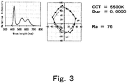
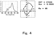
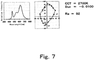
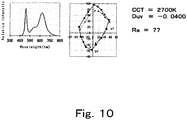
- the eight spectral power distributions shown in FIGS. 4 to 11 represent calculation results of varying D uv from -0.0500 to +0.0150 at a same CCT (2700 K) when assuming a packaged LED which incorporates a blue semiconductor light-emitting element with a peak wavelength of 459 nm and which uses the blue semiconductor light-emitting element as an excitation light source of a green phosphor and a red phosphor.
- Expected color appearances of the 15 color samples when assuming illumination at the respective spectral power distributions (test lights) and illumination by calculational reference lights corresponding to the respective test lights are as represented in the CIELAB color spaces in FIGS. 4 to 11 .
- test lights shown in FIGS. 7 to 11 represent examples where D uv is shifted in a negative direction from -0.0100 to -0.0500.
- D uv is shifted in the negative direction
- the present inventor mathematically examined predictions of color appearances of the 15 most vivid color samples which are positioned outermost in the Munsell renotation color system when assigning various D uv values to test lights in which spectrum-forming light-emitting elements (light-emitting materials) differ from each other while comparing with calculational reference lights.
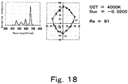
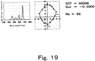
- the 10 spectral power distributions shown in FIGS. 12 to 21 represent results of varying D uv from -0.0500 to +0.0400 at a same CCT (4000 K) when a packaged LED incorporating four semiconductor light-emitting elements is assumed. Peak wavelengths of the four semiconductor light-emitting elements were respectively set to 459 nm, 528 m, 591 nm, and 662 nm. Expected color appearances of the 15 color samples when assuming illumination by the 10 respective test lights and illumination by the calculational reference lights corresponding to the respective test lights are as represented in the CIELAB color spaces in FIGS. 12 to 21 . In the drawings, points connected by dotted lines represent results obtained with the calculational reference lights and points connected by solid lines represent results regarding the respective test lights. Moreover, while a direction perpendicular to the plane of paper represents lightness, only a* and b* axes were plotted for the sake of convenience.
- test lights shown in FIGS. 17 to 21 represent examples where D uv is shifted in a negative direction from -0.0100 to -0.0500.
- D uv is shifted in the negative direction
- the present inventor mathematically examined predictions of color appearances of the 15 most vivid color samples which are positioned outermost in the Munsell renotation color system when assigning various D uv values to test lights in which spectrum-forming light-emitting elements (light-emitting materials) further differ from each other while comparing with calculational reference light.
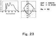
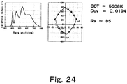
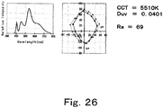
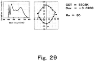
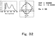
- the 11 spectral power distributions shown in FIGS. 22 to 32 represent calculation results of varying D uv from -0.0448 to +0.0496 at a close CCT (approximately 5500 K) when assuming a packaged LED which incorporates a purple semiconductor light-emitting element and which uses the purple semiconductor light-emitting element as an excitation light source of a blue phosphor, a green phosphor, and a red phosphor.
- a peak wavelength of the incorporated semiconductor light-emitting element was set to 405 nm.
- the result shown in FIG. 32 was obtained without including a green phosphor in order to cause D uv to take an excessively negative value.
- test lights shown in FIGS. 28 to 32 represent examples where D uv is shifted in a negative direction from -0.0100 to -0.0448.
- an a* value and a b* value of the 15 color samples in a CIE 1976 L*a*b* color space of test light as measured at a position of an object when the object is illuminated by the test light (according to the illumination method of the present invention) and test light when a light-emitting device emits the test light in a main radiant direction (according to the light-emitting device of the present invention) be respectively denoted by a* nSSL and b* nSSL (where n is a natural number from 1 to 15), hue angles of the 15 color samples be respectively denoted by ⁇ nSSL (degrees) (where n is a natural number from 1 to 15), an a* value and a b* value of the 15 color samples in a CIE 1976 L*a*b* color space when mathematically assuming illumination by calculational reference light that is selected according to a CCT of the test light (black-body radiator when lower than 5000 K and CIE daylight when equal to
- ⁇ C max a maximum saturation difference value among the 15 Munsell renotation color samples
- ⁇ C min a minimum saturation difference value among the 15 Munsell renotation color samples
- the index A cg is an attempt to describe a difference between a color appearance by experimental reference light or experimental pseudo-reference light and a color appearance by test light as a radiometric property and a photometric property of a spectral power distribution or a spectrum shape.
- the index A cg has been defined in the present invention as follows.
- ⁇ ref ( ⁇ ) and ⁇ SSL ( ⁇ ) respectively denote spectral power distributions of calculational reference light and test light which represent color stimuli that differ from one another when measured at a position of an illuminated object (according to the illumination method of the present invention) or when measuring light emitted in a main radiant direction from a light-emitting device (according to the light-emitting device of the present invention), x( ⁇ ), y( ⁇ ), and z( ⁇ ) denote a color-matching function, and (X ref , Y ref , Z ref ) and (X SSL , Y SSL , Z SSL ) respectively denote tristimulus values corresponding to the calculational reference light and the test light.
- index A cg was defined as follows.
- a cg ⁇ ⁇ 1 ⁇ 2 ⁇ S ⁇ d ⁇ + ⁇ ⁇ 2 ⁇ 3 ⁇ ⁇ S ⁇ d ⁇ + ⁇ ⁇ 3 ⁇ 4 ⁇ S ⁇ d ⁇
- upper and lower limit wavelengths of the integrals were respectively set to
- ⁇ 4 was defined divided into the following two cases.
- S SSL ( ⁇ ) when a wavelength which provides a longest wavelength local maximum value within 380 nm to 780 nm is denoted by ⁇ R (nm) and a spectral intensity of the wavelength ⁇ R (nm) is denoted by S SSL ( ⁇ R ), a wavelength which is on a longer wavelength-side of ⁇ R and which has an intensity of S SSL ( ⁇ R )/2 was adopted as ⁇ 4. If no such wavelength exists within a range up to 780 nm, then ⁇ 4 was set to 780 nm.
- the index A cg is used when a visible range related to radiations that are color stimuli is roughly divided into a short wavelength range (or the blue region including purple and the like), an intermediate wavelength range (the green region including yellow and the like), and a long wavelength range (the red region including orange and the like) in order to determine whether a concave and/or a convex shape of a spectrum exist at an appropriate intensity and at an appropriate position in a normalized test light spectral power distribution as compared to a mathematically normalized reference light spectral power distribution.
- long wavelength integral ranges differ according to positions of a longest wavelength local maximum value.
- selections of calculational reference light differ according to a CCT of test light. In the case of FIG.
- a first term of A cg (an integral of ⁇ S( ⁇ )) is more likely to have a negative value when a spectrum intensity of the normalized test light spectral power distribution is higher than that of the mathematically normalized reference light spectral power distribution.
- a second term of A cg (an integral of - ⁇ S( ⁇ )) is more likely to have a negative value when a spectrum intensity of the normalized test light spectral power distribution is lower than that of the normalized reference light spectral power distribution.
- a third term of A cg (an integral of ⁇ S( ⁇ )) is more likely to have a negative value when a spectrum intensity of the normalized test light spectral power distribution is higher than that of the normalized reference light spectral power distribution.
- the calculational reference light varies according to the CCT of the test light.
- black-body radiator is used as the calculational reference light when the CCT of the test light is lower than 5000 K
- defined CIE daylight is used as the calculational reference light when the CCT of the test light is equal to or higher than 5000 K.
- K Km ⁇ ⁇ 380 780 ⁇ SSL ⁇ ⁇ V ⁇ d ⁇ / ⁇ 380 780 ⁇ SSL ⁇ d ⁇
- the luminous efficacy of radiation K (lm/W) of the test light spectral power distribution ⁇ SSL ( ⁇ ) when measured at a position of an illuminated object (according to the illumination method of the present invention) or when measuring light emitted in a main radiant direction from a light-emitting device (according to the light-emitting device of the present invention) is an amount that equals luminous efficacy of a source ⁇ (lm/W) when an efficiency of the spectral power distribution which is attributable to its shape and which is related to characteristics of all materials constituting the light-emitting device (for example, efficiencies such as internal quantum efficiency and light extraction efficiency of a semiconductor light-emitting element, internal quantum efficiency and external quantum efficiency of a phosphor, and light transmission characteristics of an encapsulant) is 100%.
- prototypes of a packaged LED light source and a lighting fixture were made based on the mathematically examined spectra (test lights) .
- prototypes of a light source for light with a high R a and a high R i and which produces a color appearance that is close to that of calculational reference light as well as prototypes of a lighting fixture incorporating the light source were also made.
- prototypes of a light source that excites a green phosphor and a red phosphor using a blue semiconductor light-emitting element, a light source that excites a yellow phosphor and a red phosphor using a blue semiconductor light-emitting element, and a light source that excites a blue phosphor, a green phosphor, and a red phosphor using a purple semiconductor light-emitting element were made and instrumentalized.
- BAM or SBCA was used as the blue phosphor.
- BSS, ⁇ -SiAlON, or BSON was used as the green phosphor.
- YAG was used as the yellow phosphor.
- CASON or SCASN was used as the red phosphor.
- a normally practiced method was used when making packaged LED prototypes. Specifically, a semiconductor light-emitting element (chip) was flip-chip-mounted on a ceramic package which incorporated metal wiring capable of providing electric contact. Next, a slurry created by mixing a phosphor to be used and a binder resin was arranged as a phosphor layer.
- the packaged LEDs were used to create LED bulbs of MR16 Gu10, and MR16 Gu5.3.
- the LED bulbs were made into a type of a lighting fixture by building a drive circuit into the LED bulbs and also mounting a reflecting mirror, a lens, and the like to the LED bulbs.
- some commercially available LED bulbs were also prepared.
- incandescent bulbs incorporating a tungsten filament were also prepared to be used as experimental reference light.
- a large number of the LED bulbs were arranged to produce a lighting system for conducting comparative visual experiments.
- the lighting system was configured such that an ND filter can be disposed under the lighting fixture in order to illuminate the observation object at a low illuminance.
- a system capable of illumination by instantaneously switching among three kinds of bulbs was assembled.
- a type of drive power wire was dedicated for an incandescent bulb having a tungsten filament (experimental reference light), and an adjustable transformer was arranged at a subsequent stage so that the CCT can be varied by boosting drive voltage from 110 V to 130 V relative to 100 V input voltage.
- two remaining lines of the drive power wire were used for the LED bulbs, in which one system was used for experimental pseudo-reference light (LED light source) and the other for test light.
- comparative visual experiment were conducted in which subjects were asked to evaluate color appearances of a large number of observation objects while switching between experimental reference light (or experimental pseudo-reference light) and test light.
- the lighting system was installed in a dark room in order to remove disturbance.
- illuminance at the positions of the observation objects was set approximately the same by varying the number of fixtures of experimental reference light (or experimental pseudo-reference light) and test light which were mounted to the lighting system.
- the experiment was conducted within an illuminance range of approximately 5 lx to approximately 150 lx.
- Illuminated objects and observed objects which were actually used will be listed below. Due consideration was given to preparing chromatic objects so that colors of all hues including purple, bluish purple, blue, greenish blue, green, yellowish green , yellow, reddish yellow, red, and reddish purple were represented. Achromatic objects such as white objects and black objects were also prepared. In addition, these objects were prepared in wide varieties and in large numbers including still objects, fresh flowers, food, clothing, and printed material. Furthermore, the skins of the subjects (Japanese) themselves were also included in the experiment as observation objects. Moreover, the color names partially added to the object names listed below simply signify that such objects will appear in such colors in ordinary environments and are not accurate representations of the colors.
- the prepared experimental reference light, experimental pseudo-reference light, and test light were divided per CCT as measured at the position of illuminated objects (according to the illumination method of the present invention) or lights emitted in the main radiant directions among the prepared experimental reference light, experimental pseudo-reference light, and test light were divided per CCT (according to the light-emitting device of the present invention) into six experiments. Details are as follows.
- Table 1 CCT classification in visual experiments Experiment CCT range (K) A 2500 or higher lower than 2600 B 2600 or higher lower than 2700 C 2700 or higher lower than 2900 D 2900 or higher lower than 3250 E 3500 or higher lower than 4100 F 5400 or higher lower than 5700
- results of comparative visual experiments conducted in the third step using the prototypes of LED light sources/fixtures/systems made in the second step were compiled.
- Table 2 represents results corresponding to experiment A and Table 3 represents results corresponding to experiment B.
- Table 7 represents results corresponding to experiment F.
- a comparable appearance is represented by a central "0”
- an evaluation that the test light is slightly favorable is represented by "1”
- an evaluation that the test light is favorable is represented by "2”
- an evaluation that the test light is more favorable is represented by "3”
- an evaluation that the test light is extremely favorable is represented by "4"
- an evaluation that the test light is dramatically favorable is represented by "5".
- an evaluation that the test light is slightly unfavorable is represented by "-1"
- an evaluation that the test light is unfavorable is represented by "-2”
- an evaluation that the test light is more unfavorable is represented by "-3”
- an evaluation that the test light is extremely unfavorable is represented by "-4”
- an evaluation that the test light is dramatically unfavorable is represented by "-5”.
- the fourth step in particular, an attempt was made to extract a radiometric property and a photometric property of a spectral power distribution shared by the test light from an actually measured spectrum in a case where the color appearance of an illuminated object when illuminated by the test light was judged to be more favorable than when illuminated by experimental reference light or experimental pseudo-reference light in a visual experiment.
- test lights and comparative test lights in the tables may sometimes be collectively referred to as a "test light".
- Tables 4, 5, and 7 include results in which the D uv of test light is on the positive side of experimental reference light (or experimental pseudo-reference light). From these results, it is found that the greater the positive value of the D uv of the test light, the less favorable the color appearance or the object appearance of the illuminated object as judged by the subjects. A more specific description will be given below.
- the subjects judged that the greater the positive value of D uv , the more yellowish (greenish) the appearance and the greater a feeling of strangeness.
- the subjects judged that differences in lightness became less visible.
- the subjects pointed out that characters in illuminated printed matter became more illegible.
- the subjects judged that the greater the positive value of the D uv of the test light, the duller the color appearances as compared to when illuminated by experimental reference light (or experimental pseudo-reference light) .
- the subjects pointed out that their illuminated own skin colors appeared unnatural and unhealthy.
- the subjects pointed out that differences in color of foods with similar and analogous colors (for example, different individuals of the same type of bell pepper, carrot, etc.) became less distinguishable as compared to when illuminated by experimental reference light.
- Tables 2 to 7 include results in which the D uv of test light is on the negative side of experimental reference light (or experimental pseudo-reference light). These results show that when the D uv of the test light was in an appropriate negative range and the various indices in the tables were in appropriate ranges, the subjects judged the color appearance or the object appearance of the illuminated object to be slightly favorable, favorable, more favorable, extremely favorable, or dramatically favorable. On the other hand, it is also shown that even if the D uv of the test light was in a similar range, the color appearance or the object appearance of the illuminated object was judged to be unfavorable when the various indices in the tables were not in appropriate ranges as shown in Table 5.
- the feeling of brightness at an approximately identical illuminance was confirmed as an overall impression of the illuminated object.
- the index A cg and the luminous efficacy of radiation K (lm/W) are favorably within appropriate ranges.
- test lights which produced a favorable color appearance or a favorable object appearance had the following characteristics with respect to the color appearance of the 15 color samples when illumination by calculational reference light is assumed and the color appearance of the 15 color samples when illumination by an actually measured test light spectral power distribution is assumed.
- individual saturations ( ⁇ C n ) of the 15 color samples also show that none of the respective ⁇ C n of the 15 color samples when illuminated by the test lights was excessively lower or higher than the same values when illuminated by the calculational reference light and were all in appropriate ranges.
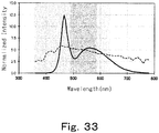
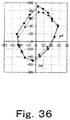
- a solid line in FIG. 35 represents a normalized test light spectral power distribution of test light 3 judged to be "dramatically favorable" in the comprehensive judgment shown in Table 3.
- a dotted line in FIG. 35 represents a normalized spectral power distribution of calculational reference light (black-body radiator) calculated based on a CCT of the test light.
- FIG. 36 represents a CIELAB plot related to color appearances of the 15 color samples when assuming illumination by the test light 3 (solid line) and assuming illumination by the calculational reference light (black-body radiator) (dotted line).
- a direction perpendicular to the plane of paper represents lightness, only a* and b* axes were plotted for the sake of convenience.
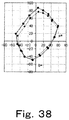
- FIGS. 37 and 38 summarize results of test light 11 judged to be “dramatically favorable” in the comprehensive judgment shown in Table 5 in a similar manner to that described above
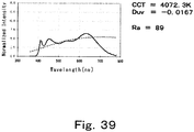
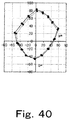
- FIGS. 39 and 40 summarize results of test light 15 judged to be “dramatically favorable” in the comprehensive judgment shown in Table 6 in a similar manner to that described above.
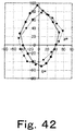
- FIGS. 41 and 42 represent a result of a CIELAB plot performed with respect to a normalized spectral power distribution and color appearances of the 15 color samples for the comparative test light 18 in a similar manner to FIGS.
- D uv in the illumination method according to the first embodiment of the present invention was -0.0070 or lower, favorably -0.00778 or lower, more favorably -0.0105 or lower, extremely favorably -0.0126 or lower, and dramatically favorably -0.0166 or lower.
- D uv in the illumination method according to the first embodiment of the present invention was -0.0430 or higher, or -0.04268 or higher, favorably -0.0389 or higher, more favorably -0.0334 or higher, extremely favorably -0.0285 or higher, and dramatically favorably -0.0250 or higher.
- in the illumination method according to the first embodiment of the present invention was 9.2 or lower, extremely favorably 8.4 or lower, and dramatically favorably 7.7 or lower.
- is more favorable and that each
- in the illumination method according to the first embodiment of the present invention was 0 or higher and a minimum value thereof during the visual experiments was 0.00292. Furthermore, an examination performed using actual test light during the visual experiments revealed that a favorable range of each
- ⁇ n 1 15 ⁇ C n 15 in the illumination method according to the first embodiment of the present invention was 1.7 or higher, favorably 1.9 or higher, extremely favorably 2.3 or higher, and dramatically favorably 2.6 or higher; and
- Each ⁇ C n in the illumination method according to the first embodiment of the present invention was -2.7 or higher, extremely favorably -2.5 or higher, and dramatically favorably -1.2 or higher.
- each ⁇ C n in the illumination method according to the first embodiment of the present invention was 22.3 or lower, favorably 20.3 or lower, and dramatically favorably 16.9 or lower.
- an examination performed using actual test light during the visual experiments revealed that a favorable range of each ⁇ C n within favorable experiment results under examination was -2.4 or higher and 20.2 or lower.
- ( ⁇ C max - ⁇ C min ) in the illumination method according to the first embodiment of the present invention was 21.8 or lower
- ( ⁇ C max - ⁇ C min ) was favorably 19.8 or lower, and dramatically favorably 17.9 or lower.
- a lower ( ⁇ C max - ⁇ C min ) is more favorable and that ( ⁇ C max - ⁇ C min ) is more dramatically favorably 15.0 or lower and extremely dramatically favorably 14.0 or lower.
- ( ⁇ C max - ⁇ C min ) in the illumination method according to the first embodiment of the present invention was 3.0 or higher
- ( ⁇ C max - ⁇ C min ) was favorably 3.3 or higher
- a minimum value thereof during the visual experiments was 3.36.
- D uv was as considered heretofore and was -0.0070 or lower, favorably -0.00778 or lower, more favorably -0.0105 or lower, extremely favorably -0.0126 or lower, and dramatically favorably -0.0166 or lower.
- D uv in the illumination method according to the first embodiment of the present invention was -0.0430 or higher, or -0.04268 or higher, favorably -0.0389 or higher, more favorably -0.0334 or higher, extremely favorably -0.0285 or higher, and dramatically favorably -0.0250 or higher.
- a cg assumes a negative value in an appropriate range means that there are appropriate existence of a concave and/or a convex shape in a normalized test light spectral power distribution, and radiant flux intensity of the normalized test light spectral power distribution tends to be higher than that of a mathematical normalized reference light spectral power distribution in a short wavelength range between 380 nm and 495 nm, and/or radiant flux intensity of the normalized test light spectral power distribution tends to be lower than that of a mathematical normalized reference light spectral power distribution in an intermediate wavelength range between 495 nm and 590 nm, and/or radiant flux intensity of the normalized test light spectral power distribution tends to be higher than that of a mathematical normalized reference light spectral power distribution in a long wavelength range between 590 nm and ⁇ 4.
- a cg is a sum of respective elements in the short wavelength range, the intermediate wavelength range, and the long wavelength range, individual elements may not necessarily exhibit the tendencies described above. Based on the above, it is understood that a favorable color appearance or a favorable object appearance was produced when A cg is quantitatively -25 or lower and -461 or higher.
- a cg in the illumination method according to the first embodiment of the present invention was preferably -25 or lower, more favorably -28 or lower, extremely favorably -41 or lower, and dramatically favorably -114 or lower.
- a cg was preferably -461 or higher, favorably -420 or higher, more favorably -323 or higher, extremely favorably -254 or higher, and dramatically favorably -248 or higher.
- the luminous efficacy of radiation of the spectral power distributions produced by the illumination method according to the first embodiment of the present invention favorably ranged from 174 (lm/W) to 318 (lm/W) and was higher by approximately 15% or more than 150 (lm/W) which is a value of an ordinary incandescent bulb or the like.
- the reason for this is believed to be that radiation from the semiconductor light-emitting element and radiation from the phosphor were internal.
- the reason for this is also believed to be that an appropriate concave and/or convex shape was present at an appropriate position in the spectral power distributions with respect to a relationship with V ( ⁇ ). From the perspective of achieving a balance with color appearance, the luminous efficacy of radiation in the illumination method according to the present invention favorably ranged as described below.
- the luminous efficacy of radiation K in the illumination method according to the first embodiment of the present invention was preferably 174 (lm/W) or higher
- the luminous efficacy of radiation K was favorably 193 (lm/W) or higher, more favorably 204 (lm/W) or higher, extremely favorably 208 (lm/W) or higher, and dramatically favorably 209 (lm/W) or higher.
- the luminous efficacy of radiation K in the present invention was preferably 318 (lm/W) or lower. In consideration of achieving a balance with color appearance, the luminous efficacy of radiation K was more favorably 290 (lm/W) or lower, and dramatically favorably 258 (lm/W) or lower.
- CCT in the illumination method according to the first embodiment of the present invention.
- ⁇ n 1 15 ⁇ C n 15 can be increased while keeping
- a CCT in the illumination method according to the first embodiment of the present invention ranges slightly favorably from 1800 K to 15000 K, favorably from 2000 K to 10000 K, more favorably from 2300 K to 7000 K, extremely favorably from 2600 K to 6600 K, dramatically favorably from 2900 K to 5800 K, and most favorably from 3400 K to 5100 K.
- the indices A cg described in Tables 2 to 7 must be within appropriate ranges in addition to D uv .
- the various indices namely, the luminous efficacy of radiation K (lm/W) ,
- , ⁇ n 1 15 ⁇ C n 15 , ⁇ C n , and ( ⁇ C max - ⁇ C min ) are favorably within appropriate ranges.
- results of the test lights judged to be favorable in the visual experiments revealed the following with respect to D uv and the index A cg .
- D uv was as considered heretofore and was -0.0070 or lower, favorably -0.00778 or lower, more favorably -0.0105 or lower, extremely favorably -0.0126 or lower, and dramatically favorably -0.0166 or lower.
- D uv in the light-emitting device according to the second embodiment of the present invention was -0.0430 or higher, or -0.04268 or higher, favorably -0.0389 or higher, more favorably -0.0334 or higher, extremely favorably -0.0285 or higher, and dramatically favorably -0.0250 or higher.
- a cg assumes a negative value in an appropriate range means that there are appropriate existence of a concave and/or a convex shape in a normalized test light spectral power distribution, and radiant flux intensity of the normalized test light spectral power distribution tends to be higher than that of a mathematical normalized reference light spectral power distribution in a short wavelength range between 380 nm and 495 nm, and/or radiant flux intensity of the normalized test light spectral power distribution tends to be lower than that of a mathematical normalized reference light spectral power distribution in an intermediate wavelength range between 495 nm and 590 nm, and/or radiant flux intensity of the normalized test light spectral power distribution tends to be higher than that of a mathematical normalized reference light spectral power distribution in a long wavelength range between 590 nm and ⁇ 4. Based on the above, it is understood that a favorable color appearance or a favorable object appearance was produced when A cg is quantitatively -25 or lower and -461 or higher.
- a cg as derived from a spectral power distribution of light emitted in a main radiant direction from the light-emitting device according to the second embodiment of the present invention was -25 or lower, more favorably -28 or lower, extremely favorably -41 or lower, and dramatically favorably -114 or lower.
- a cg as derived from a spectral power distribution of light emitted in a main radiant direction from the light-emitting device according to the second embodiment of the present invention was -461 or higher, favorably -420 or higher, more favorably -323 or higher, extremely favorably -254 or higher, and dramatically favorably -248 or higher.
- the luminous efficacy of radiation of the spectral power distribution produced by the light-emitting device according to the second embodiment of the present invention favorably ranged from 174 (lm/W) to 318 (lm/W) and was higher by approximately 15% or more than 150 (lm/W) which is a value of an ordinary incandescent bulb or the like.
- the reason for this is believed to be that radiation from the semiconductor light-emitting element and radiation from the phosphor were internal.
- the reason for this is also believed to be that an appropriate concave and/or convex shape was present at an appropriate position in the spectral power distributions with respect to a relationship with V ( ⁇ ).
- the luminous efficacy of radiation as obtained from a spectral power distribution of light emitted in a main radiant direction by the light-emitting device according to the second embodiment of the present invention favorably ranged as described below.
- the luminous efficacy of radiation K produced by the light-emitting device according to the second embodiment of the present invention was preferably 174 (lm/W) or higher
- the luminous efficacy of radiation K was favorably 193 (lm/W) or higher, more favorably 204 (lm/W) or higher, extremely favorably 208 (lm/W) or higher, and dramatically favorably 209 or higher.
- the luminous efficacy of radiation K in the present invention was preferably 318 (lm/W) or lower. In consideration of achieving a balance with color appearance, the luminous efficacy of radiation K was more favorably 290 (lm/W) or lower, and dramatically favorably 258 (lm/W) of lower.
- test lights which produced a favorable color appearance or a favorable object appearance had the following characteristics with respect to the color appearance of the 15 color samples when illumination by calculational reference light is assumed and the color appearance of the 15 color samples when illumination by an actually measured test light spectral power distribution is assumed.
- individual saturations ( ⁇ C n ) of the 15 color samples also show that none of the respective ⁇ C n of the 15 color samples when illuminated by the test lights was excessively lower or higher than the same values when illuminated by the calculational reference light and were all in appropriate ranges.
- a solid line in FIG. 35 represents a normalized test light spectral power distribution of the test light 3 judged to be "dramatically favorable" in the comprehensive judgment shown in Table 3.
- a dotted line in FIG. 35 represents a normalized spectral power distribution of calculational reference light (black-body radiator) calculated based on a CCT of the test light.
- FIG. 36 represents a CIELAB plot related to color appearances of the 15 color samples when assuming illumination by the test light 3 (solid line) and assuming illumination by the calculational reference light (black-body radiator) (dotted line).
- a direction perpendicular to the plane of paper represents lightness, only a* and b* axes were plotted for the sake of convenience.
- FIGS. 37 and 38 summarize results of the test light 11 judged to be “dramatically favorable” in the comprehensive judgment shown in Table 5 in a similar manner to that described above
- FIGS. 39 and 40 summarize results of the test light 15 judged to be “dramatically favorable” in the comprehensive judgment shown in Table 6 in a similar manner to that described above.
- FIGS. 41 and 42 represent a result of a CIELAB plot performed with respect to a normalized spectral power distribution and color appearances of the 15 color samples for the comparative test light 18 in a similar manner to FIGS. 35 , 36 , and the like. As is apparent from FIGS.
- D uv in the light-emitting device according to the second embodiment of the present invention was -0.0070 or lower, favorably -0.00778 or lower, more favorably -0.0105 or lower, extremely favorably -0.0126 or lower, and dramatically favorably -0.0166 or lower.
- D uv in the light-emitting device according to the second embodiment of the present invention was -0.0070 or lower, favorably -0.00778 or lower, more favorably -0.0105 or lower, extremely favorably -0.0126 or lower, and dramatically favorably -0.0166 or lower.
- D uv in the light-emitting device according to the second embodiment of the present invention was -0.0430 or higher, or -0.04268 or higher, favorably -0.0389 or higher, more favorably -0.0334 or higher, extremely favorably -0.0285 or higher, and dramatically favorably -0.0250 or higher.
- in the light-emitting device according to the second embodiment of the present invention was preferably 9.2 or lower, extremely favorably 8.4 or lower, and dramatically favorably 7.7 or lower.
- is more favorable and that each
- in the light-emitting device according to the second embodiment of the present invention was preferably 0 or higher and a minimum value thereof during the visual experiments was 0.00292. Furthermore, an examination performed using actual test light during the visual experiments revealed that a favorable range of each
- ⁇ n 1 15 ⁇ C n 15 in the light-emitting device according to the second embodiment of the present invention was: preferably 1.7 or higher, favorably 1.9 or higher, extremely favorably 2.3 or higher, and dramatically favorably 2.6 or higher; and preferably 8.2 or lower, favorably 7.5 or lower, extremely favorably 6.4 or lower, and dramatically favorably 5.1 or lower.
- Each ⁇ C n in the light-emitting device according to the second embodiment of the present invention was preferably - 2.7 or higher, extremely favorably -2.5 or higher, and dramatically favorably -1.2 or higher.
- each ⁇ C n in the light-emitting device according to the second embodiment of the present invention was preferably 22.3 or lower, favorably 20.3 or lower, and dramatically favorably 16.9 or lower.
- ( ⁇ C max - ⁇ C min ) in the light-emitting device according to the second embodiment of the present invention was preferably 21.8 or lower
- ( ⁇ C max - ⁇ C min ) was favorably 19.8 or lower, and dramatically favorably 17.9 or lower.
- a lower ( ⁇ C max - ⁇ C min ) is more favorable and that ( ⁇ C max - ⁇ C min ) is more dramatically favorably 15.0 or lower and extremely dramatically favorably 14.0 or lower.
- ( ⁇ C max - ⁇ C min ) in the light-emitting device according to the second embodiment of the present invention was preferably 3.0 or higher, favorably 3.3 or higher, and dramatically favorably 4.0 or higher and a minimum value thereof during the visual experiments was 3.36.
- an examination performed using actual test light during the visual experiments revealed that a favorable range of ( ⁇ C max - ⁇ C min ) within favorable experiment results under examination is 3.4 or higher and 19.7 or lower.
- ⁇ n 1 15 ⁇ C n 15 can be increased while keeping
- a CCT in the light-emitting device ranges slightly favorably from 1800 K to 15000 K, favorably from 2000 K to 10000 K, more favorably from 2300 K to 7000 K, extremely favorably from 2600 K to 6600 K, dramatically favorably from 2900 K to 5800 K, and most favorably from 3400 K to 5100 K.
- the illumination method according to the present invention no restrictions are placed on configurations, materials, and the like of the light-emitting device as long as a photometric property of test light which is irradiated on an illuminated object and which becomes a color stimulus is in an appropriate range and, at the same time, a difference between color appearances of the 15 color samples when illumination by calculational reference light is assumed and color appearances of the 15 color samples when illumination by an actually measured test light spectral power distribution is assumed is in an appropriate range.
- the light-emitting device With the light-emitting device according to the present invention, no restrictions are placed on configurations, materials, and the like of the light-emitting device as long as a radiometric property and a photometric property of test light which is irradiated from the light-emitting device in a main radiant direction and which becomes a color stimulus with respect to an illuminated object are in appropriate ranges.
- a light-emitting device for implementing the illumination method or the light-emitting device according to the present invention such as an illumination light source, a lighting fixture including the illumination light source, or a lighting system including the illumination light source or the lighting fixture is not restricted in any way, but preferably includes at least one semiconductor light-emitting element that is a light-emitting element.
- the illumination light source including the semiconductor light-emitting element may be configured such that a plurality of semiconductor light-emitting elements of different types such as blue, green, and red is incorporated in one illumination light source or may be configured such that a blue semiconductor light-emitting element is included in one illumination light source, a green semiconductor light-emitting element is included in another illumination light source, and a red semiconductor light-emitting element is included in yet another illumination light source, whereby the semiconductor light-emitting elements are integrated with a lens, a reflecting mirror, a drive circuit, and the like in a light fixture and provided to a lighting system.
- semiconductor light-emitting elements are integrated with a lens, a reflecting mirror, a drive circuit, and the like in a light fixture and provided to a lighting system.
- a lighting system may be configured such that light radiated as the lighting system satisfies desired characteristics at a position of an illuminated object due to additive color mixing with light from a different lighting fixture that exists in the lighting system or the lighting system may be configured such that light in a main radiant direction among light radiated as the lighting system satisfies desired characteristics.
- light as a color stimulus which is ultimately irradiated on an illuminated object or light in a main radiant direction among light emitted from the light-emitting device need only satisfy appropriate conditions according to the present invention.
- a light-emitting device for implementing the illumination method according to the first embodiment of the present invention or the light-emitting device according to the second embodiment of the present invention favorably includes a light-emitting element (light-emitting material) which has a peak within a short wavelength range from ⁇ 1 (380 nm) to A2 (495 nm), another light-emitting element (light-emitting material) which has a peak within an intermediate wavelength range from ⁇ 2 (495 nm) to ⁇ 3 (590 nm), and yet another light-emitting element (light-emitting material) which has a peak within a long wavelength range from ⁇ 3 (590 nm) to 780 nm.
- a light-emitting element light-emitting material
- another light-emitting element which has a peak within an intermediate wavelength range from ⁇ 2 (495 nm) to ⁇ 3 (590 nm)
- yet another light-emitting element (light-emitting material) which has
- a light-emitting device for implementing the illumination method according to the first embodiment of the present invention or the light-emitting device according to the second embodiment of the present invention favorably includes at least one each of light-emitting elements (light-emitting materials) which have emission peaks in the three respective wavelength ranges described above, more favorably includes one light-emitting element (light-emitting material) in each of two wavelength ranges among the three wavelength ranges and a plurality of light-emitting elements (light-emitting materials) in the one remaining wavelength range, extremely favorably includes one light-emitting element (light-emitting material) in one wavelength range among the three wavelength ranges and a plurality of light-emitting elements (light-emitting materials) in each of the two remaining wavelength ranges, and dramatically favorably includes a plurality of light-emitting elements (light-emitting materials) in all three wavelength ranges. This is because by incorporating light-emitting elements such that two or more peak wavelengths exist in one range, controll
- an actual light-emitting device that uses a semiconductor light-emitting element as a phosphor excitation light source, favorably, there are two types of phosphors in one light-emitting device and there are peak wavelengths in each of the three wavelength ranges including the wavelength of the semiconductor light-emitting element.
- an actual light-emitting device is configured using only semiconductor light-emitting elements with different peak wavelengths.
- the number of different types of semiconductor light-emitting elements in one light source is favorably three or more, more favorably four or more, extremely favorably five or more, and dramatically favorably six or more. Having seven or more different types creates a hassle when mounting on a light source or the like and therefore becomes unfavorable.
- a light-emitting device may be configured with two types of semiconductor light-emitting elements.
- semiconductor light-emitting elements and phosphors can be mixed and mounted at will.
- a blue light-emitting element and two types of phosphors may be mounted in one light source, or a blue light-emitting element and three types of phosphors (green, red 1, and red 2) may be mounted in one light source.
- a purple light-emitting element and four types of phosphors blue, green, red 1, and red 2 may be mounted in one light source.
- one light source may incorporate a portion mounted with a blue light-emitting element and two types of phosphors (green and red) and a portion mounted with a purple light-emitting element and three types of phosphors (blue, green, and red).
- light-emitting elements in each of the three wavelength ranges favorably include at least one light-emitting element with a relatively narrow band.
- two ranges among the three respective wavelength ranges include a relatively narrow band light-emitting element and, even more favorably, all of the three respective wavelength ranges include a relatively narrow band light-emitting element.
- a relatively narrow band light-emitting element may itself individually constitute a light-emitting element in a given wavelength region, more favorably, a plurality of types of relatively narrow band light-emitting elements exist in the wavelength region and, equally more favorably, a relatively narrow band light-emitting element and a relatively broad band light-emitting element coexist in the wavelength region.
- a "relatively narrow band” as used herein refers to a full-width at half-maximum of a light-emitting element (light-emitting material) being equal to or less than 2/3 of 115 nm, 95 nm, and 190 nm which are respective range widths of the short wavelength range (380 nm to 495 nm), the intermediate wavelength range (495 nm to 590 nm), and the long wavelength range (590 nm to 780 nm).
- a full-width at half-maximum of the light-emitting element with respect to the respective range widths is favorably 1/2 or less, more favorably 1/3 or less, extremely favorably 1/4 or less, and dramatically favorably 1/5 or less.
- the full-width at half-maximum is favorably 2 nm or more, more favorably 4 nm or more, extremely favorably 6 nm or more, and dramatically favorably 8 nm or more.
- the following light-emitting materials, phosphor materials, and semiconductor light-emitting elements are favorably incorporated in the light-emitting device as light-emitting elements.
- light emitted from all light sources can be included, such as thermal emission light from a hot filament or the like, electric discharge emission light from a fluorescent tube, a high-pressure sodium lamp, or the like, stimulated emission light from a laser or the like, spontaneous emission light from a semiconductor light-emitting element, and spontaneous emission light from a phosphor.
- emission of light from a photoexcited phosphor, emission of light from a photoexcited semiconductor light-emitting element, and emission of light from a photoexcited semiconductor laser are favorable due to their small sizes, high energy efficiency, and their ability to emit light in a relatively narrow band.
- a semiconductor light-emitting element include a purple light-emitting element (with a peak wavelength of around 395 nm to 420 nm), a bluish purple light-emitting element (with a peak wavelength of around 420 nm to 455 nm), or a blue light-emitting element (with a peak wavelength of around 455 nm to 485 nm) in which an In(Al)GaN material formed on a sapphire substrate or a GaN substrate is included in an active layer structure.
- a blue light-emitting element (with a peak wavelength of around 455 nm to 485 nm) in which a Zn(Cd) (S) Se material formed on a GaAs substrate is included in an active layer structure is also favorable.
- a spectral power distribution or a peak wavelength of a radiant flux produced by a light-emitting element (light-emitting material) such as a semiconductor light-emitting element or a phosphor normally fluctuates slightly depending on ambient temperature, a heat dissipation environment of the light-emitting device including a package and a fixture, injected current, circuit architecture and, in some cases, deterioration or the like. Therefore, a semiconductor light-emitting element with a peak wavelength of 418 nm under a certain drive condition may exhibit a peak wavelength of, for example, 421 nm when temperature of ambient environment rises.
- a spectral power distribution or a peak wavelength of a radiant flux produced by light-emitting elements such as the semiconductor light-emitting elements and phosphors described below.
- the active layer structure may be any of a multiple quantum well structure in which a quantum well layer and a barrier layer are laminated, a single or a double heterostructure including a relatively thick active layer and a barrier layer (or a clad layer), and a homo junction constituted by a single pn junction.
- the active layer includes an In(Al) GaN material
- a bluish purple light-emitting element and a purple light-emitting element in which In concentration decreases in the active layer structure as compared to a blue light-emitting element are favorable since emission wavelength fluctuation due to segregation by In decreases and a full-width at half-maximum of the emission spectrum becomes narrower.
- a bluish purple light-emitting element and a purple light-emitting element are favorable because wavelengths are positioned closer to a relatively outer side (short wavelength-side) of the wavelength range from 380 nm to 495 nm and D uv can be easily controlled.
- a semiconductor light-emitting element having an emission peak in the short wavelength range from ⁇ 1 (380 nm) to A2 (495 nm) in the present invention is favorably a blue light-emitting element (with a peak wavelength of around 455 nm to 485 nm), more favorably a bluish purple light-emitting element (with a peak wavelength of around 420 nm to 455 nm) with a shorter wavelength, and extremely favorably a purple light-emitting element (with a peak wavelength of around 395 nm to 420 nm) with a shorter wavelength. Furthermore, it is also favorable to use a plurality of types of these light-emitting elements.
- a semiconductor laser is also favorably used as the light-emitting element and, for the same reasons as described above, the semiconductor laser is favorably a blue semiconductor laser (with an emission wavelength of around 455 nm to 485 nm), more favorably a bluish purple semiconductor laser (with an emission wavelength of around 420 nm to 455 nm) with a longer wavelength, and extremely favorably a purple semiconductor laser (with an emission wavelength of around 395 nm to 420 nm) with a longer wavelength.
- a full-width at half-maximum of an emission spectrum of the semiconductor light-emitting element is favorably narrow.
- the full-width at half-maximum of the semiconductor light-emitting element used in the short wavelength range is favorably 45 nm or less, more favorably 40 nm or less, extremely favorably 35 nm or less, and dramatically favorably 30 nm or less.
- the full-width at half-maximum of the semiconductor light-emitting element used in the short wavelength range is favorably 2 nm or more, more favorably 4 nm or more, extremely favorably 6 nm or more, and dramatically favorably 8 nm or more.
- the short wavelength range semiconductor light-emitting element that is used in the illumination method or the light-emitting device according to the present invention favorably includes an In(Al)GaN material in an active layer structure
- the semiconductor light-emitting element is favorably a light-emitting element formed on a sapphire substrate or a GaN substrate.
- the degree of In segregation in the active layer of a light-emitting element formed on a GaN substrate is more favorable than when formed on a sapphire substrate. This is dependent on the degree of lattice matching between the substrate and active layer structure material.
- the substrate is favorably either thick or completely separated from the semiconductor light-emitting element.
- the substrate when creating a short wavelength range semiconductor light-emitting element on a GaN substrate, in order to facilitate light extraction from side walls of the GaN substrate, the substrate is favorably thick and is 100 ⁇ m or more, more favorably 200 ⁇ m or more, extremely favorably 400 ⁇ m or more, and dramatically favorably 600 ⁇ m or more.
- the substrate thickness is favorably 2 mm or less, more favorably 1.8 mm or less, extremely favorably 1.6 mm or less, and dramatically favorably 1.4 mm or less.
- the substrate is favorably separated using a method such as laser lift-off.
- a method such as laser lift-off.
- Such a configuration reduces stress acting on the quantum well layer which facilitates widening of bandwidth due to an extreme lattice mismatch with the substrate and, as a result, a narrower band spectrum of the light-emitting element can be achieved. Therefore, with a light-emitting element separated from a sapphire substrate or the like, a dramatic synergistic effect with the present invention can be expected and is therefore extremely favorable.
- a full-width at half-maximum of the phosphor material is favorably narrow.
- the full-width at half-maximum of an emission spectrum of the phosphor material used in the short wavelength range when photoexcited at room temperature is favorably 90 nm or less, more favorably 80 nm or less, extremely favorably 70 nm or less, and dramatically favorably 60 nm or less.
- the full-width at half-maximum of the phosphor material used in the short wavelength range is favorably 2 nm or more, more favorably 4 nm or more, extremely favorably 6 nm or more, and dramatically favorably 8 nm or more.
- the phosphor material favorably has a peak wavelength in the following ranges.
- the peak wavelength favorably ranges from 455 nm to 485 nm and more favorably has a shorter wavelength from 420 nm to 455 nm.
- the peak wavelength favorably ranges from 455 nm to 485 nm, more favorably has a shorter wavelength from 420 nm to 455 nm, and extremely favorably has a shorter wavelength from 395 nm to 420 nm.
- the short wavelength range phosphor material used in the illumination method or the light-emitting device according to the present invention while any phosphor material satisfying the full-width at half-maximum described above can be favorably used, one specific example is a blue phosphor which uses Eu 2+ as an activator and a crystal constituted by alkaline-earth aluminate or alkaline-earth halophosphate as a host.
- examples include a phosphor represented by the following general formula (5), a phosphor represented by the following general formula (5)', (Sr,Ba) 3 MgSi 2 O 8 :Eu 2+ , and (Ba, Sr, Ca, Mg) Si 2 O 2 N 2 :Eu. (Ba, Sr, Ca) MgAl 10 O 17 :Mn, Eu (5) (An alkaline-earth aluminate phosphor represented by the general Formula (5) is referred to as a BAM phosphor).
- X is Cl.
- c, d, and x are numbers satisfying 2.7 ⁇ c ⁇ 3.3, 0.9 ⁇ d ⁇ 1.1, and 0.3 ⁇ x ⁇ 1.2.
- Favorable examples include a BAM phosphor, a SBCA phosphor, and a SCA phosphor, which are the phosphors described above, as well as a Ba-SION phosphor ((Ba,Sr,Ca,Mg)Si 2 O 2 N 2 :Eu) and a (Sr,Ba) 3 MgSi 2 O 8 :Eu 2+ phosphor.
- light emitted from all light sources can be included, such as thermal emission light from a hot filament or the like, electric discharge emission light from a fluorescent tube, a high-pressure sodium lamp, or the like, stimulated emission light from a laser or the like including second-order harmonic generation (SHG) using a non-linear optical effect or the like, spontaneous emission light from a semiconductor light-emitting element, and spontaneous emission light from a phosphor.
- thermal emission light from a hot filament or the like such as thermal emission light from a hot filament or the like, electric discharge emission light from a fluorescent tube, a high-pressure sodium lamp, or the like, stimulated emission light from a laser or the like including second-order harmonic generation (SHG) using a non-linear optical effect or the like, spontaneous emission light from a semiconductor light-emitting element, and spontaneous emission light from a phosphor.
- SHG second-order harmonic generation
- emission of light from a photoexcited phosphor emission of light from a photoexcited semiconductor light-emitting element, emission of light from a photoexcited semiconductor laser, and emission of light from a photoexcited SHG laser are favorable due to their small sizes, high energy efficiency, and their ability to emit light in a relatively narrow band.
- a semiconductor light-emitting element include a greenish blue light-emitting element (with a peak wavelength of around 495 nm to 500 nm), a green light-emitting element (with a peak wavelength of around 500 nm to 530 nm), a yellowish green light-emitting element (with a peak wavelength of around 530 nm to 570 nm), or a yellow light-emitting element (with a peak wavelength of around 570 nm to 580 nm) in which an In(Al)GaN material on a sapphire substrate or a GaN substrate is included in an active layer structure.
- a yellowish green light-emitting element (with a peak wavelength of around 530 nm to 570 nm) due to GaP on a GaP substrate or a yellow light-emitting element (with a peak wavelength of around 570 nm to 580 nm) due to GaAsP on a GaP substrate is also favorable. Furthermore, a yellow light-emitting element (with a peak wavelength of around 570 nm to 580 nm) due to AlInGaP on a GaAs substrate is also favorable.
- the active layer structure may be any of a multiple quantum well structure in which a quantum well layer and a barrier layer are laminated, a single or a double heterostructure including a relatively thick active layer and a barrier layer (or a clad layer), and a homo junction constituted by a single pn junction.
- a yellowish green light-emitting element, a green light-emitting element, and a greenish blue light-emitting element in which In concentration decreases in the active layer structure as compared to a yellow light-emitting element are favorable since emission wavelength fluctuation due to segregation by In decreases and a full-width at half-maximum of the emission spectrum becomes narrower.
- a semiconductor light-emitting element having an emission peak in the intermediate wavelength range from A2 (495 nm) to A3 (590 nm) in the present invention is favorably a yellow light-emitting element (with a peak wavelength of around 570 nm to 580 nm), more favorably a yellowish green light-emitting element (with a peak wavelength of around 530 nm to 570 nm) with a shorter wavelength, extremely favorably a green light-emitting element (with a peak wavelength of around 500 nm to 530 nm) with a shorter wavelength, and dramatically favorably a greenish blue light-emitting element (with a peak wavelength of around 495 nm to 500 nm).
- an emission wavelength is favorably within a yellow range (with a peak wavelength of around 570 nm to 580 nm), more favorably within a yellowish green range (with a peak wavelength of around 530 nm to 570 nm) with a shorter wavelength, extremely favorably within a green range (with a peak wavelength of around 500 nm to 530 nm) with a shorter wavelength, and dramatically favorably within a greenish blue range (with a peak wavelength of around 495 nm to 500 nm).
- a full-width at half-maximum of an emission spectrum of the semiconductor light-emitting element is favorably narrow.
- the full-width at half-maximum of the semiconductor light-emitting element used in the intermediate wavelength range is favorably 75 nm or less, more favorably 60 nm or less, extremely favorably 50 nm or less, and dramatically favorably 40 nm or less.
- the full-width at half-maximum of the semiconductor light-emitting element used in the intermediate wavelength range is favorably 2 nm or more, more favorably 4 nm or more, extremely favorably 6 nm or more, and dramatically favorably 8 nm or more.
- the semiconductor light-emitting element is favorably a light-emitting element formed on a sapphire substrate or a GaN substrate.
- a light-emitting element formed on a GaN substrate is particularly favorable.
- an InAlGaN element formed on a GaN substrate reduces a piezoelectric effect attributable to a difference in lattice constants from the substrate and enables suppression of spatial separation of electrons/holes when injecting a carrier into a quantum well layer as compared to an InAlGaN element formed on a sapphire substrate. As a result, a full-width at half-maximum of the emission wavelength can be narrowed.
- the substrate is favorably either thick or completely removed.
- the substrate when creating an intermediate wavelength range semiconductor light-emitting element on a GaN substrate, in order to facilitate light extraction from side walls of the GaN substrate, the substrate is favorably thick and is 100 ⁇ m or more, more favorably 200 ⁇ m or more, extremely favorably 400 ⁇ m or more, and dramatically favorably 600 ⁇ m or more.
- the substrate thickness is favorably 2 mm or less, more favorably 1.8 mm or less, extremely favorably 1.6 mm or less, and dramatically favorably 1.4 mm or less.
- the substrate is favorably thick and is 100 ⁇ m or more, more favorably 200 ⁇ m or more, extremely favorably 400 ⁇ m or more, and dramatically favorably 600 ⁇ m or more.
- the substrate thickness is favorably 2 mm or less, more favorably 1.8 mm or less, extremely favorably 1.6 mm or less, and dramatically favorably 1.4 mm or less.
- the substrate is favorably thin or completely separated from the semiconductor light-emitting element.
- the substrate is favorably separated using a method such as laser lift-off.
- a method such as laser lift-off.
- Such a configuration reduces stress acting on the quantum well layer which causes widening of bandwidth due to an extreme lattice mismatch with the substrate and, as a result, a narrower band spectrum of the light-emitting element can be achieved. Therefore, with a semiconductor light-emitting element separated from a sapphire substrate or the like, a dramatic synergistic effect with the present invention can be expected and is therefore extremely favorable.
- a full-width at half-maximum of the phosphor material is favorably narrow.
- the full-width at half-maximum of an emission spectrum of the phosphor material used in the intermediate wavelength range when photoexcited at room temperature is favorably 130 nm or less, more favorably 110 nm or less, extremely favorably 90 nm or less, and dramatically favorably 70 nm or less.
- the full-width at half-maximum of the phosphor material used in the intermediate wavelength range is favorably 2 nm or more, more favorably 4 nm or more, extremely favorably 6 nm or more, and dramatically favorably 8 nm or more.
- a peak wavelength of the phosphor material favorably ranges from 495 nm to 500 nm.
- a peak wavelength ranging from 500 nm to 530 nm and a peak wavelength ranging from 570 nm to 580 nm are both more favorable to similar degrees, and a peak wavelength ranging from 530 nm to 570 nm is extremely favorable.
- any phosphor material satisfying the full-width at half-maximum described above can be favorably used.
- such specific examples include a green phosphor containing Eu 2+ , Ce 3+ , or the like as an activator.
- a preferable green phosphor using Eu 2+ as an activator is a green phosphor which uses a crystal constituted by alkaline-earth silicate, alkaline-earth nitride silicate, or SiAlON as a host.
- a green phosphor of this type can normally be excited using a semiconductor light-emitting element ranging from ultraviolet to blue.
- alkaline-earth silicate crystal as a host
- a phosphor represented by the following general formula (6) and a phosphor represented by the following general formula (6)'.
- Alkaline-earth silicate represented by the general formula (6) is referred to as a BSS phosphor) .
- SiAlON crystal examples include a phosphor represented by Si 6-z Al z O z N 8-z :Eu (where 0 ⁇ z ⁇ 4.2) (this phosphor is referred to as a ⁇ -SiAlON phosphor) .
- Preferable green phosphors using Ce 3+ as an activator include a green phosphor with a garnet-type oxide crystal as a host such as Ca 3 (Sc,Mg) 2 Si 3 O 12 :Ce or a green phosphor with an alkaline-earth scandate crystal as a host such as CaSc 2 O 4 :Ce.
- Other examples include SrGaS 4 :Eu 2+ .
- Still other examples include an oxynitride phosphor represented by (Ba,Ca,Sr,Mg,Zn,Eu) 3 Si 6 O 12 N 2 (this phosphor is referred to as a BSON phosphor).
- Yet other examples include a yttrium aluminum garnet phosphor represented by (Y 1-u Gd u ) 3 (Al 1-v Ga v ) 5 O 12 : Ce, Eu (where u and v respectively satisfy 0 ⁇ u ⁇ 0.3 and 0 ⁇ v ⁇ 0.5) (this phosphor is referred to as a YAG phosphor) and a lanthanum silicon nitride phosphor represented by Ca 1.5x La 3-X Si 6 N 11 :Ce (where x satisfies 0 ⁇ x ⁇ 1) (this phosphor is referred to as an LSN phosphor.)
- favorable examples include a BSS phosphor, a ⁇ -SiAlON phosphor, a BSON phosphor, a G-BAM phosphor, a YAG phosphor, and a SrGaS 4 :Eu 2+ phosphor.
- light emitted from all light sources can be included, such as thermal emission light from a hot filament or the like, electric discharge emission light from a fluorescent tube, a high-pressure sodium lamp, or the like, stimulated emission light from a laser or the like, spontaneous emission light from a semiconductor light-emitting element, and spontaneous emission light from a phosphor.
- emission of light from a photoexcited phosphor, emission of light from a photoexcited semiconductor light-emitting element, and emission of light from a photoexcited semiconductor laser are favorable due to their small sizes, high energy efficiency, and their ability to emit light in a relatively narrow band.
- an orange light-emitting element (with a peak wavelength of around 590 nm to 600 nm) or a red light-emitting element (from 600 nm to 780 nm) in which an AlGaAs material formed on a GaAs substrate or an (Al) InGaP material formed on a GaAs substrate is included in an active layer structure is favorable.
- a red light-emitting element (from 600 nm to 780 nm) in which an GaAsP material formed on a GaP substrate is included in an active layer structure is favorable.
- the active layer structure may be any of a multiple quantum well structure in which a quantum well layer and a barrier layer are laminated, a single or a double heterostructure including a relatively thick active layer and a barrier layer (or a clad layer), and a homo junction constituted by a single pn junction.
- a peak wavelength is favorably close to a vicinity of 630 nm in consideration of achieving a balance between D uv controllability and luminous efficacy of radiation. From this perspective, a red light-emitting element is more favorable than an orange light-emitting element.
- a semiconductor light-emitting element having an emission peak in the long wavelength range from A3 (590 nm) to 780 nm in the present invention is favorably an orange light-emitting element (with a peak wavelength of around 590 nm to 600 nm), more favorably a red light-emitting element (with a peak wavelength of around 600 nm to 780 nm), and extremely favorably a red light-emitting element with a peak wavelength that is close to around 630 nm.
- a red light-emitting element with a peak wavelength ranging from 615 nm to 645 nm is extremely favorable.
- a semiconductor laser is also favorably used as a light-emitting element.
- an emission wavelength is favorably within an orange range (with a peak wavelength of around 590 nm to 600 nm), more favorably within a red range (with a peak wavelength of around 600 nm to 780 nm), and extremely favorably within a red range in which a peak wavelength is close to around 630 nm.
- a red semiconductor laser with a peak wavelength ranging from 615 nm to 645 nm is extremely favorable.
- a full-width at half-maximum of an emission spectrum of the semiconductor light-emitting element is favorably narrow.
- the full-width at half-maximum of the semiconductor light-emitting element used in the long wavelength range is favorably 30 nm or less, more favorably 25 nm or less, extremely favorably 20 nm or less, and dramatically favorably 15 nm or less.
- the full-width at half-maximum of the semiconductor light-emitting element used in the long wavelength range is favorably 2 nm or more, more favorably 4 nm or more, extremely favorably 6 nm or more, and dramatically favorably 8 nm or more.
- the substrate is favorably thin or completely removed.
- a full-width at half-maximum of the phosphor material is favorably narrow.
- the full-width at half-maximum of an emission spectrum of the phosphor material used in the long wavelength range when photoexcited at room temperature is favorably 130 nm or less, more favorably 110 nm or less, extremely favorably 90 nm or less, and dramatically favorably 70 nm or less.
- the full-width at half-maximum of the phosphor material used in the long wavelength range is favorably 2 nm or more, more favorably 4 nm or more, extremely favorably 6 nm or more, and dramatically favorably 8 nm or more.
- a peak wavelength is extremely favorably close to 630 nm in consideration of achieving a balance between D uv controllability and luminous efficacy of radiation.
- a phosphor material having an emission peak in a long wavelength range from A3 (590 nm) to 780 nm in the present invention has a peak that is favorably between 590 nm and 600 nm and more favorably around 600 nm to 780 nm, and a peak wavelength is extremely favorably close to 630 nm.
- a phosphor material with a peak wavelength ranging from 620 nm to 655 nm is extremely favorable.
- any phosphor material satisfying the full-width at half-maximum described above can be favorably used.
- specific examples include phosphors using Eu 2+ as an activator and a crystal constituted by alkaline-earth silicon-nitride, ⁇ SiAlON, or alkaline-earth silicate as a host.
- a red phosphor of this type can normally be excited using a semiconductor light-emitting element ranging from ultraviolet to blue.
- phosphors using an alkaline-earth silicon-nitride crystal as a host include a phosphor represented by (Ca,Sr,Ba,Mg)AlSiN 3 :Eu and/or (Ca,Sr,Ba)AlSiN 3 :Eu (this phosphor is referred to as a SCASN phosphor), a phosphor represented by (CaAlSiN 3 ) 1-x (Si 2 N 2 O) x :Eu (where x satisfies 0 ⁇ x ⁇ 0.5) (this phosphor is referred to as a CASON phosphor), a phosphor represented by (Sr,Ca,Ba) 2 Al x Si 5-x O x N 8-x :Eu (where 0 ⁇ x ⁇ 2), and a phosphor represented by Eu y (Sr,Ca,Ba) 1-y :Al 1+x Si 4-x O x N
- a Mn 4+ -activated fluoride complex phosphor is a phosphor which uses Mn 4+ as an activator and a fluoride complex salt of an alkali metal, amine, or an alkaline-earth metal as a host crystal.
- Fluoride complex salts which form the host crystal include those whose coordination center is a trivalent metal (B, Al, Ga, In, Y, Sc, or a lanthanoid), a tetravalent metal (Si, Ge, Sn, Ti, Zr, Re, or Hf), and a pentavalent metal (V, P, Nb, or Ta), and the number of fluorine atoms coordinated around the center ranges from 5 to 7.
- a favorable Mn 4+ -activated fluoride complex phosphor is A 2+x M y Mn z F n (where A is Na and/or K; M is Si and Al; and -1 ⁇ x ⁇ 1 and 0.9 ⁇ y + z ⁇ 1.1 and 0.001 ⁇ z ⁇ 0.4 and 5 ⁇ n ⁇ 7) which uses a hexafluoro complex of an alkali metal as a host crystal.
- a phosphor represented by the following general formula (7) and a phosphor represented by the following general formula (7)'.
- (La 1-x-y Eu x Ln y ) 2 O 2 S (7) (In the general formula (7), x and y denote numbers respectively satisfying 0.02 ⁇ x ⁇ 0.50 and 0 ⁇ y ⁇ 0.50, and Ln denotes at least one trivalent rare-earth element among Y, Gd, Lu, Sc, Sm, and Er).
- a lanthanum oxysulfide phosphor represented by the general formula (7) is referred to as an LOS phosphor).
- k, x, and y denote numbers respectively satisfying 2.8 ⁇ k ⁇ 5, 0.1 ⁇ x ⁇ 0.7, and 0.005 ⁇ y ⁇ 0.015
- A is any of calcium (Ca), strontium (Sr), barium (Ba), zinc (Zn), and a mixture consisted of these elements).
- a germanate phosphor represented by the general formula (7) is referred to as an MGOF phosphor).
- favorable examples include a LOS phosphor, an MGOF phosphor, a KSF phosphor, a KSNAF phosphor, a SCASN phosphor, a CASON phosphor, a (Sr,Ca,Ba) 2 Si 5 N 8 :Eu phosphor and a (Sr,Ca,Ba)AlSi 4 N 7 phosphor.
- a purple LED with a peak wavelength of around 395 nm to 420 nm
- at least one or more phosphors selected from a group of relatively narrow band phosphors consisting of ⁇ -SiAlON, BSS, BSON, and G-BAM in the light source as a light-emitting element in the intermediate wavelength range
- at least one or more phosphors selected from the group consisting of CASON, SCASN, LOS, KSF, and KSNAF in the light source as a light-emitting element in the long wavelength range.
- a purple LED with a peak wavelength of around 395 nm to 420 nm
- SBCA that is a relatively narrow band phosphor in a light source
- ⁇ -SiAlON that is a relatively narrow band phosphor as a first light-emitting element in the intermediate wavelength range
- CASON CASON as a first light-emitting element in the long wavelength range
- a purple LED with a peak wavelength of around 395 nm to 420 nm
- SCA that is a relatively narrow band phosphor in a light source
- ⁇ -SiAlON that is a relatively narrow band phosphor as a first light-emitting element in the intermediate wavelength range
- CASON CASON as a first light-emitting element in the long wavelength range
- a purple LED with a peak wavelength of around 395 nm to 420 nm
- BAM that is a relatively narrow band phosphor in a light source
- BSS that is a relatively narrow band phosphor
- CASON CASON
- a bluish purple LED with a peak wavelength of around 420 nm to 455 nm
- a blue LED with a peak wavelength of around 455 nm to 485 nm
- incorporate at least one or more phosphors selected from a group of relatively narrow band phosphors consisting of ⁇ -SiAlON, BSS, BSON, and G-BAM in a light source as a light-emitting element in the intermediate wavelength range and incorporate at least one or more phosphors selected from the group consisting of CASON, SCASN, LOS, KSF, and KSNAF in the light source as a light-emitting element in the long wavelength range.
- a bluish purple LED with a peak wavelength of around 420 nm to 455 nm
- a blue LED with a peak wavelength of around 455 nm to 485 nm
- BSON that is a relatively narrow band phosphor
- SCASN as a first light-emitting element in the long wavelength range
- a bluish purple LED with a peak wavelength of around 420 nm to 455 nm
- a blue LED with a peak wavelength of around 455 nm to 485 nm
- ⁇ -SiAlON that is a relatively narrow band phosphor
- CASON CASON
- a bluish purple LED with a peak wavelength of around 420 nm to 455 nm
- a blue LED with a peak wavelength of around 455 nm to 485 nm
- ⁇ -SiAlON that is a relatively narrow band phosphor
- CASON as a first light-emitting element in the long wavelength range
- KSF or KSNAF as a second light-emitting element in the long wavelength range.
- a bluish purple LED with a peak wavelength of around 420 nm to 455 nm
- a blue LED with a peak wavelength of around 455 nm to 485 nm
- ⁇ -SiAlON that is a relatively narrow band phosphor
- SCASN as a first light-emitting element in the long wavelength range
- a bluish purple LED with a peak wavelength of around 420 nm to 455 nm
- a blue LED with a peak wavelength of around 455 nm to 485 nm
- ⁇ -SiAlON that is a relatively narrow band phosphor
- SCASN as a first light-emitting element in the long wavelength range
- KSF or KSNAF as a second light-emitting element in the long wavelength range.
- peak wavelength positions, full-widths at half-maximum, and the like of the respective light-emitting elements are extremely advantageous in realizing a color appearance or an object appearance perceived as favorable by the subjects in the visual experiments.
- the illumination method or the light-emitting device it is favorable to use the light-emitting elements (light-emitting materials) heretofore described because the index A cg , the luminous efficacy of radiation K (lm/W), D uv , and the like can be more readily set to desired values.
- a relative emission intensity of the light-emitting element in the short wavelength range can be increased, a relative emission intensity of the light-emitting element in the long wavelength range can be increased, a relative emission intensity of the light-emitting element in the intermediate wavelength range can be decreased, or the like.
- the emission position of the light-emitting element in the short wavelength range may be moved toward a shorter wavelength side and, at the same time, the emission position of the light-emitting element in the long wavelength range may be moved toward a longer wavelength side, or the like.
- operations opposite to those described above may be performed to vary D uv toward a positive side.
- D uv can be lowered by, for example, increasing a relative intensity of a light-emitting element on a relatively shorter wavelength side among the two light-emitting elements in the short wavelength range, increasing a relative intensity of a light-emitting element on a relatively longer wavelength side among the two light-emitting elements in the long wavelength range, or the like.
- the relative intensity of the light-emitting element on a relatively shorter wavelength side among the two light-emitting elements in the short wavelength range is increased and, at the same time, the relative intensity of the light-emitting element on a relatively longer wavelength side among the two light-emitting elements in the long wavelength range is increased.
- operations opposite to those described above may be performed to vary D uv toward a positive side.
- ⁇ n 1 15 ⁇ C n 15 , ⁇ C n , and ( ⁇ C max - ⁇ C min ) which are related to a difference between color appearances of the 15 color samples when illumination by the light-emitting device is assumed and color appearances when illumination by calculational reference light is assumed and, in particular, as means for increasing ⁇ C n , operations such as described below can be performed after adjusting an entire spectral power distribution so that D uv assumes a desired value.
- Operations which may be performed include replacing each light-emitting element with a material having a narrow full-width at half-maximum, forming a spectrum shape in which light-emitting elements are appropriately separated from each other, installing a filter that absorbs a desired wavelength in an illumination light source, a lighting fixture, or the like in order to form a concave and/or a convex shape in a spectrum of each light-emitting element, and additionally mounting a light-emitting element which performs emission at a narrower band in a light-emitting element.
- the present invention reveals a primary illumination method or a primary light-emitting device for improving, with respect to a wide variety of illuminated objects with various hues, visibility of an object to be illuminated, providing a better color appearance of chromatic colors perceived by a human, and improving a feeling of brightness within an illuminance range of 5 lx to 150 lx for which visual experiments have been carried out.
- Means for achieving this involve setting D uv of light at a position of an illuminated object to within an appropriate range and, at the same time, setting indices related to a difference between color appearances of the 15 color samples when illumination by the light is assumed and color appearances when illumination by calculational reference light is assumed such as
- , ⁇ n 1 15 ⁇ C n 15 , ⁇ C n , and ( ⁇ C max - ⁇ C min ) to within appropriate ranges.
- the illumination method according to the present invention is an illumination method in which light emitted from a semiconductor light-emitting element is included in the spectral power distribution as a constituent element and, at the same time, the illumination method according to the present invention is an illumination method of illuminating light in which
- , ⁇ n 1 15 ⁇ C n 15 , ⁇ C n , ( ⁇ C max - ⁇ C min ), D uvSSL , and the like are within appropriate ranges to an illuminated object, and a light-emitting device used in the illumination method according to the present invention can be configured in any way as long as the device is capable of providing such illumination.
- the device may be any of an individual illumination light source, an illuminating module in which at least one or more of the light sources is mounted on a heatsink or the like, and a lighting fixture in which a lens, a light-reflecting mechanism, a driving electric circuit, and the like are added to the light source or the module .
- the device may be a lighting system which is a collection of individual light sources, individual modules, individual fixtures, and the like and which at least has a mechanism for supporting such components.
- the light-emitting device is a light-emitting device in which means for improving visibility, providing a better color appearance of chromatic colors perceived by a human and improving a feeling of brightness involve setting D uv as obtained from a spectral power distribution of light emitted in a main radiant direction to within an appropriate range and, at the same time, setting the index A cg to within an appropriate range.
- the light-emitting device may be configured in any way as long as the light-emitting device includes light emitted from semiconductor light-emitting elements as a spectral component in a spectral power distribution in a main radiant direction and in which D uv derived from a spectral power distribution of light which is in the radiant direction and the index A cg are in appropriate ranges.
- the device may be any of an individual illumination light source, an illuminating module in which at least one or more of the light sources is mounted on a heatsink or the like, and a lighting fixture in which a lens, a light-reflecting mechanism, a driving electric circuit, and the like are added to the light source or the module.
- the device may be a lighting system which is a collection of individual light sources, individual modules, individual fixtures, and the like and which at least has a mechanism for supporting such components.
- the illumination method or the light-emitting device such as an illumination light source, a lighting fixture, a lighting system, and the like according to the present invention has an extremely wide field of application and may be used without being limited to particular uses. However, in consideration of the features of the illumination method or the light-emitting device according to the present invention, the illumination method or the light-emitting device according to the present invention is favorably applied to the following fields.
- favorable applications include a reading light in a bedroom and work lighting such as a torch during emergency work.
- work lighting such as a torch during emergency work.
- illumination by the illumination method or the light-emitting device according to the present invention makes color identification among close hues easier and realizes a work environment as though in a high-illuminance environment even under a low illuminance (e.g. , approximately 100 lx) with low energy consumption. Even from such a perspective, applications to work lighting are favorable.
- color discrimination ability increases, for example, applications to medical lighting such as a light source used in a gastroscope or the like are also favorable. While arterial blood is vivid red due to its high oxygen content, venous blood is dark red due to its high carbon dioxide content. Although arterial blood and venous blood are both red, chromas of the colors differ from each other. Therefore, with the illumination method or device according to the present invention which achieves favorable color appearance (chroma), it is expected that arterial blood and venous blood can be readily distinguished from each other. In addition, since it is obvious that favorable color representation in color image information such as an endoscope has a significant effect on diagnosis, it is expected that a normal location and a lesion location can be readily distinguished from each other.
- the illumination method can be favorably applied to an illumination method used in industrial equipments such as a product image judgment device.
- a number of determination errors occurring during image determination can be kept as small as a number of determination errors occurring in a high illuminance environment.
- a good color appearance is achieved for a majority of, and in some cases, all colors such as purple, bluish purple, blue, greenish blue, green, yellowish green , yellow, reddish yellow, red, and reddish purple even when illuminance only ranges from 5 lx to 150 lx.
- the skin color of the subjects Japanese
- various foods, clothing, wood colors, and the like which have intermediate chroma also acquire natural color appearances which many of the subjects feel more favorable.
- the illumination method or the light-emitting device according to the present invention to ordinary lighting for homes and the like, it is conceivable that food may appear fresher and more appetizing, newspapers, magazines, and the like may become more legible, and visibility of differences in level in the house may increase, thereby contributing to improving home safety even under a low-illuminance environment with low energy consumption. Accordingly, the present invention is favorably applied to home lighting. In addition, the present invention is also favorable as exhibit lighting to attractively illuminate clothing, food, vehicles, suitcases, shoes, ornaments, furniture, and the like with low illuminance while suppressing the electric consumption at a shop, and enables lighting which makes such items stand out from their surroundings.
- the present invention is also favorable as lighting for goods such as cosmetics in which slight differences in color are the decisive factor when purchasing the goods. Furthermore, the present invention is also favorable as presentation lighting at a wedding center, a theater, and the like, and enables kimonos, makeup in kabuki or the like to appear vividly while the electric consumption is suppressed. The present invention also favorably highlights skin tones. In addition, by using the present invention as lighting in a hair salon, colors that are no different than those perceived outdoors can be obtained during hair coloring and excessive dyeing or insufficient dyeing can be prevented.
- the present invention is favorably applicable as interior lighting in such public transport.
- the present invention is also favorably applicable as lighting for aged persons.
- the illumination method or the light-emitting device according to the present invention can be applied to lighting in public facilities or the like which are used by the general public such as a waiting room in a retirement house or a hospital, a book store, and a library.
- the illumination method or the light-emitting device according to the present invention can be favorably used in applications for securing visibility by adapting to an illumination environment in which illuminance is often at a relatively low level due to various circumstances.
- street lamps and the like tend to conserve energy by emitting a low illuminance of approximately 10 lx on a ground surface.
- Using the light-emitting device or the illumination method according to the present invention for such applications is preferred.
- the illumination method or the light-emitting device according to the present invention is favorably applied to head lights of vehicles to increase visibility as compared to using conventional light sources.
- the present invention can also be used favorably in a foot light that is lit in a movie theater or the like during a screening.
Landscapes
- Chemical & Material Sciences (AREA)
- Inorganic Chemistry (AREA)
- Engineering & Computer Science (AREA)
- Materials Engineering (AREA)
- Organic Chemistry (AREA)
- Led Device Packages (AREA)
- Luminescent Compositions (AREA)
- Circuit Arrangement For Electric Light Sources In General (AREA)
- Non-Portable Lighting Devices Or Systems Thereof (AREA)
- Optical Filters (AREA)
Claims (3)
- Procédé de conception d'un dispositif d'émission de lumière incorporant un élément d'émission de lumière, caractérisé en ce qu'il comprend les étapes consistant à :configurer une lumière émise par le dispositif d'émission de lumière de manière à inclure, dans une direction rayonnante principale de celui-ci, de la lumière dont la distance DuvSSL d'un locus de rayonnement de corps noir tel que défini par la norme ANSI C78.377 satisfait à -0,04268 ≤ DuvSSL ≤ -0,0070, etsi une distribution spectrale d'énergie de la lumière émise par le dispositif d'émission de lumière dans la direction rayonnante est désignée par φSSL(λ), une distribution spectrale d'énergie d'une lumière de référence qui est sélectionnée selon TSSL(K) de la lumière émise par le dispositif d'émission de lumière dans la direction rayonnante est désignée par φref(λ), des valeurs tristimulus de la lumière émise par le dispositif d'émission de lumière dans la direction rayonnante sont désignées par (XSSL, YSSL, ZSSL) et des valeurs tristimulus de la lumière de référence qui est sélectionnée selon TSSL (K) de la lumière émise par le dispositif d'émission de lumière dans la direction rayonnante sont désignées par (Xref, Yref, Zref), etsi une distribution spectrale d'énergie normalisée SSSL (λ) de la lumière émise par le dispositif d'émission de lumière dans la direction rayonnante, une distribution spectrale d'énergie normalisée Sref (λ) d'une lumière de référence qui est sélectionnée selon TSSL (K) de la lumière émise du dispositif d'émission de lumière dans la direction rayonnante, et une différence ΔS(λ) entre ces distributions spectrales d'énergie normalisées sont respectivement définies comme


 si une longueur d'onde qui produit une valeur maximale locale de longueur d'onde la plus longue de SSSL (λ) dans une plage de longueurs d'onde de 380 nm à 780 nm est désignée par λR (nm), alors déterminer une longueur d'onde Λ4 qui satisfait à SSSL (Λ4) = SSSL (λR)/2 et existe sur un côté de longueur d'onde plus long de λR,calculer un indice Acg selon la formule (3) ci-dessous, dans lequel l'indice Acg satisfait à -461 ≤ Acg ≤ -25,
- Procédé de conception d'un dispositif d'émission de lumière incorporant un élément d'émission de lumière, caractérisé en ce qu'il comprend les étapes consistant à :configurer une lumière émise par le dispositif d'émission de lumière de manière à inclure, dans une direction rayonnante principale de celui-ci, de la lumière dont la distance DuvSSL d'un locus de rayonnement de corps noir tel que défini par la norme ANSI C78.377 satisfait à -0,04268 ≤ DuvSSL ≤ -0,0070, etsi une distribution spectrale d'énergie de la lumière émise par le dispositif d'émission de lumière dans la direction rayonnante est désignée par (φSSL (λ), une distribution spectrale d'énergie d'une lumière de référence qui est sélectionnée selon TSSL(K) de la lumière émise par le dispositif d'émission de lumière dans la direction rayonnante est désignée par φref (λ), des valeurs tristimulus de la lumière émise par le dispositif d'émission de lumière dans la direction rayonnante sont désignées par (XSSL, YSSL, ZSSL) et des valeurs tristimulus de la lumière de référence qui est sélectionnée selon TSSL (K) de la lumière émise par le dispositif d'émission de lumière dans la direction rayonnante sont désignées par (Xref, Yref, Zref), etsi une distribution spectrale d'énergie normalisée SSSL (λ) de la lumière émise par le dispositif d'émission de lumière dans la direction rayonnante, une distribution spectrale d'énergie normalisée Sref (λ) d'une lumière de référence qui est sélectionnée selon TSSL (K) de la lumière émise du dispositif d'émission de lumière dans la direction rayonnante, et une différence ΔS(λ) entre ces distributions spectrales d'énergie normalisées sont respectivement définies comme


 si une longueur d'onde qui produit une valeur maximale locale de longueur d'onde la plus longue de SSSL (λ) dans une plage de longueurs d'onde de 380 nm à 780 nm est désignée par λR (nm), alors déterminer qu'une longueur d'onde Λ4 qui satisfait à SSSL (Λ4) = SSSL (λR)/2 n'existe pas sur un côté de longueur d'onde plus long de λR,calculer un indice Acg selon la formule (4) ci-dessous, dans lequel l'indice Acg satisfait à -461 ≤ Acg ≤ -25.
- Procédé de conception d'un dispositif d'émission de lumière selon la revendication 1 ou 2, et dans lequel
la lumière émise par le dispositif d'émission de lumière dans la direction rayonnante satisfait à (1) et (2) ci-dessous :(1) si une valeur a* et une valeur b* dans l'espace colorimétrique CIE 1976 L*a*b* de 15 échantillons de couleur de renotation Munsell de #01 à #15 énumérés ci-dessous lors de l'hypothèse mathématique d'un éclairage par la lumière émise par le dispositif d'émission de lumière dans la direction rayonnante sont respectivement désignées par a*nSSL et b*nSSL (où n est un nombre naturel de 1 à 15), et
une valeur a* et une valeur b* dans l'espace colorimétrique CIE 1976 L*a*b* de 15 échantillons de couleur de renotation Munsell lors de l'hypothèse mathématique d'un éclairage par une lumière de référence qui est sélectionnée selon une température de couleur corrélée TSSL (K) de la lumière émise par le dispositif d'émission de lumière dans la direction rayonnante sont respectivement désignées par a*nref et b*nref (où n est un nombre naturel de 1 à 15), alors chaque différence de saturation ΔCn satisfait à
-2,7 ≤ ΔCn ≤ 22,3 (où n est un nombre naturel de 1 à 15),
une différence de saturation moyenne représentée par la formule (1) ci-dessous satisfait à la formule (2) ci-dessous et


#01 7,5P 4/10 #02 10PB 4/10 #03 5PB 4/12 #04 7,5B 5/10 #05 10BG 6/8 #06 2,5BG 6/10 #07 2,5G 6/12 #08 7,5GY 7/10 #09 2,5GY 8/10 #10 5Y 8,5/12 #11 10YR 7/12 #12 5YR 7/12 #13 10R 6/12 #14 5R 4/14 #15 7,5RP 4/12 (2) si des angles de teinte dans l'espace colorimétrique CIE 1976 L*a*b* des 15 échantillons de couleur de renotation Munsell lors de l'hypothèse mathématique d'un éclairage par la lumière émise par le dispositif d'émission de lumière dans la direction rayonnante sont désignés par θnSSL (degrés) (où n est un nombre naturel de 1 à 15), et
des angles de teinte dans un espace colorimétrique CIE 1976 L*a*b* des 15 échantillons de couleur de renotation Munsell lors de l'hypothèse mathématique d'un éclairage par une lumière de référence qui est sélectionnée selon la température de couleur corrélée TSSL(K) de la lumière émise dans la direction rayonnante sont désignés par θnref (degrés) (où n est un nombre naturel de 1 à 15), puis une valeur absolue de chaque différence d'angles de teinte |Δhn| satisfait à
Applications Claiming Priority (2)
| Application Number | Priority Date | Filing Date | Title |
|---|---|---|---|
| JP2012191015 | 2012-08-31 | ||
| PCT/JP2013/066601 WO2014034228A1 (fr) | 2012-08-31 | 2013-06-17 | Procédé d'éclairage et dispositif d'émission de lumière |
Publications (4)
| Publication Number | Publication Date |
|---|---|
| EP2892306A1 EP2892306A1 (fr) | 2015-07-08 |
| EP2892306A4 EP2892306A4 (fr) | 2015-10-21 |
| EP2892306B1 EP2892306B1 (fr) | 2020-12-23 |
| EP2892306B9 true EP2892306B9 (fr) | 2021-08-25 |
Family
ID=50183052
Family Applications (1)
| Application Number | Title | Priority Date | Filing Date |
|---|---|---|---|
| EP13832489.2A Active EP2892306B9 (fr) | 2012-08-31 | 2013-06-17 | Procédé d'éclairage et dispositif d'émission de lumière |
Country Status (3)
| Country | Link |
|---|---|
| EP (1) | EP2892306B9 (fr) |
| JP (3) | JP6126103B2 (fr) |
| WO (1) | WO2014034228A1 (fr) |
Families Citing this family (8)
| Publication number | Priority date | Publication date | Assignee | Title |
|---|---|---|---|---|
| JP6405738B2 (ja) * | 2014-06-19 | 2018-10-17 | 三菱ケミカル株式会社 | 発光装置 |
| EP3214359B1 (fr) * | 2014-10-28 | 2021-12-15 | Seoul Semiconductor Co., Ltd. | Source de lumière blanche et système de source de lumière blanche |
| WO2018155665A1 (fr) * | 2017-02-27 | 2018-08-30 | シチズン電子株式会社 | Dispositif électroluminescent en semiconducteur et dispositif d'éclairage |
| JP6886150B2 (ja) * | 2017-11-01 | 2021-06-16 | 伊藤光学工業株式会社 | 光学要素 |
| JP7451078B2 (ja) * | 2018-05-29 | 2024-03-18 | 日亜化学工業株式会社 | 発光装置 |
| US10879429B2 (en) | 2018-05-29 | 2020-12-29 | Nichia Corporation | Light emitting device |
| US11320100B2 (en) | 2018-12-04 | 2022-05-03 | Signify Holding B.V. | Crisp white tuning |
| JP7170525B2 (ja) * | 2018-12-18 | 2022-11-14 | シチズン時計株式会社 | Led発光装置 |
Family Cites Families (15)
| Publication number | Priority date | Publication date | Assignee | Title |
|---|---|---|---|---|
| TW383508B (en) | 1996-07-29 | 2000-03-01 | Nichia Kagaku Kogyo Kk | Light emitting device and display |
| JP2000231905A (ja) * | 1998-12-07 | 2000-08-22 | Matsushita Electric Ind Co Ltd | 蛍光ランプ |
| JP2005158795A (ja) * | 2003-11-20 | 2005-06-16 | Sumitomo Electric Ind Ltd | 発光ダイオード及び半導体発光装置 |
| TW200637033A (en) * | 2004-11-22 | 2006-10-16 | Matsushita Electric Ind Co Ltd | Light-emitting device, light-emitting module, display unit, lighting unit and method for manufacturing light-emitting device |
| JP2007141737A (ja) * | 2005-11-21 | 2007-06-07 | Sharp Corp | 照明装置、液晶表示装置、照明装置の制御方法、照明装置制御プログラム、および記録媒体 |
| JP2007299714A (ja) * | 2006-05-08 | 2007-11-15 | Osram-Melco Ltd | 照明器具 |
| JP2009099510A (ja) * | 2007-02-15 | 2009-05-07 | Toshiba Lighting & Technology Corp | 照明装置 |
| JP2009048989A (ja) * | 2007-07-20 | 2009-03-05 | Toshiba Lighting & Technology Corp | 照明装置 |
| US8373338B2 (en) * | 2008-10-22 | 2013-02-12 | General Electric Company | Enhanced color contrast light source at elevated color temperatures |
| US8410714B2 (en) * | 2007-11-12 | 2013-04-02 | Mitsubishi Chemical Corporation | Illuminating device |
| EP2398079A1 (fr) * | 2009-04-27 | 2011-12-21 | Toshiba Lighting&Technology Corporation | Dispositif d'éclairage |
| EP2432037B1 (fr) | 2009-08-26 | 2019-05-22 | Mitsubishi Chemical Corporation | Dispositif émettant de la lumière blanche à semi-conducteur |
| CN102640569B (zh) * | 2009-12-09 | 2015-07-08 | 皇家飞利浦电子股份有限公司 | 用于强调对象的方法和设备 |
| KR101114197B1 (ko) * | 2010-08-09 | 2012-02-22 | 엘지이노텍 주식회사 | 발광 소자 및 이를 구비한 조명 시스템 |
| JP5654328B2 (ja) * | 2010-11-24 | 2015-01-14 | パナソニックIpマネジメント株式会社 | 発光装置 |
-
2013
- 2013-06-17 JP JP2014532847A patent/JP6126103B2/ja active Active
- 2013-06-17 WO PCT/JP2013/066601 patent/WO2014034228A1/fr active Application Filing
- 2013-06-17 EP EP13832489.2A patent/EP2892306B9/fr active Active
-
2017
- 2017-04-06 JP JP2017075721A patent/JP6359718B2/ja active Active
-
2018
- 2018-06-20 JP JP2018116709A patent/JP6584030B2/ja active Active
Also Published As
| Publication number | Publication date |
|---|---|
| JPWO2014034228A1 (ja) | 2016-08-08 |
| JP2018198206A (ja) | 2018-12-13 |
| WO2014034228A1 (fr) | 2014-03-06 |
| JP6584030B2 (ja) | 2019-10-02 |
| EP2892306A1 (fr) | 2015-07-08 |
| EP2892306A4 (fr) | 2015-10-21 |
| JP2017138617A (ja) | 2017-08-10 |
| JP6126103B2 (ja) | 2017-05-10 |
| EP2892306B1 (fr) | 2020-12-23 |
| JP6359718B2 (ja) | 2018-07-18 |
Similar Documents
| Publication | Publication Date | Title |
|---|---|---|
| US10355177B2 (en) | Illumination method and light-emitting device | |
| US10236424B2 (en) | Illumination method and light-emitting device | |
| US10930823B2 (en) | Light-emitting device, method for designing light-emitting device, method for driving light-emitting device, illumination method, and method for manufacturing light-emitting device | |
| EP2892306B9 (fr) | Procédé d'éclairage et dispositif d'émission de lumière | |
| EP3091585A1 (fr) | Dispositif électroluminescent et procédé de conception de dispositif électroluminescent | |
| JP6632704B2 (ja) | 発光装置及び発光装置の製造方法 |
Legal Events
| Date | Code | Title | Description |
|---|---|---|---|
| PUAI | Public reference made under article 153(3) epc to a published international application that has entered the european phase |
Free format text: ORIGINAL CODE: 0009012 |
|
| 17P | Request for examination filed |
Effective date: 20141219 |
|
| AK | Designated contracting states |
Kind code of ref document: A1 Designated state(s): AL AT BE BG CH CY CZ DE DK EE ES FI FR GB GR HR HU IE IS IT LI LT LU LV MC MK MT NL NO PL PT RO RS SE SI SK SM TR |
|
| AX | Request for extension of the european patent |
Extension state: BA ME |
|
| RA4 | Supplementary search report drawn up and despatched (corrected) |
Effective date: 20150922 |
|
| RIC1 | Information provided on ipc code assigned before grant |
Ipc: C09K 11/66 20060101ALI20150916BHEP Ipc: C09K 11/73 20060101ALI20150916BHEP Ipc: C09K 11/84 20060101ALI20150916BHEP Ipc: H01L 33/50 20100101ALI20150916BHEP Ipc: C09K 11/59 20060101ALI20150916BHEP Ipc: H05B 37/02 20060101AFI20150916BHEP Ipc: C09K 11/62 20060101ALI20150916BHEP Ipc: C09K 11/64 20060101ALI20150916BHEP Ipc: C09K 11/08 20060101ALI20150916BHEP Ipc: F21S 2/00 20060101ALI20150916BHEP |
|
| RAP1 | Party data changed (applicant data changed or rights of an application transferred) |
Owner name: CITIZEN ELECTRONICS CO., LTD. |
|
| DAX | Request for extension of the european patent (deleted) | ||
| STAA | Information on the status of an ep patent application or granted ep patent |
Free format text: STATUS: EXAMINATION IS IN PROGRESS |
|
| 17Q | First examination report despatched |
Effective date: 20180815 |
|
| REG | Reference to a national code |
Ref country code: DE Ref legal event code: R079 Ref document number: 602013074914 Country of ref document: DE Free format text: PREVIOUS MAIN CLASS: H05B0037020000 Ipc: H05B0045200000 |
|
| RIC1 | Information provided on ipc code assigned before grant |
Ipc: H05B 45/20 20200101AFI20200612BHEP Ipc: H05B 47/10 20200101ALI20200612BHEP |
|
| GRAP | Despatch of communication of intention to grant a patent |
Free format text: ORIGINAL CODE: EPIDOSNIGR1 |
|
| STAA | Information on the status of an ep patent application or granted ep patent |
Free format text: STATUS: GRANT OF PATENT IS INTENDED |
|
| INTG | Intention to grant announced |
Effective date: 20200805 |
|
| GRAS | Grant fee paid |
Free format text: ORIGINAL CODE: EPIDOSNIGR3 |
|
| GRAA | (expected) grant |
Free format text: ORIGINAL CODE: 0009210 |
|
| STAA | Information on the status of an ep patent application or granted ep patent |
Free format text: STATUS: THE PATENT HAS BEEN GRANTED |
|
| AK | Designated contracting states |
Kind code of ref document: B1 Designated state(s): AL AT BE BG CH CY CZ DE DK EE ES FI FR GB GR HR HU IE IS IT LI LT LU LV MC MK MT NL NO PL PT RO RS SE SI SK SM TR |
|
| REG | Reference to a national code |
Ref country code: GB Ref legal event code: FG4D |
|
| REG | Reference to a national code |
Ref country code: DE Ref legal event code: R096 Ref document number: 602013074914 Country of ref document: DE |
|
| REG | Reference to a national code |
Ref country code: AT Ref legal event code: REF Ref document number: 1348963 Country of ref document: AT Kind code of ref document: T Effective date: 20210115 |
|
| REG | Reference to a national code |
Ref country code: IE Ref legal event code: FG4D |
|
| PG25 | Lapsed in a contracting state [announced via postgrant information from national office to epo] |
Ref country code: RS Free format text: LAPSE BECAUSE OF FAILURE TO SUBMIT A TRANSLATION OF THE DESCRIPTION OR TO PAY THE FEE WITHIN THE PRESCRIBED TIME-LIMIT Effective date: 20201223 Ref country code: FI Free format text: LAPSE BECAUSE OF FAILURE TO SUBMIT A TRANSLATION OF THE DESCRIPTION OR TO PAY THE FEE WITHIN THE PRESCRIBED TIME-LIMIT Effective date: 20201223 Ref country code: NO Free format text: LAPSE BECAUSE OF FAILURE TO SUBMIT A TRANSLATION OF THE DESCRIPTION OR TO PAY THE FEE WITHIN THE PRESCRIBED TIME-LIMIT Effective date: 20210323 Ref country code: GR Free format text: LAPSE BECAUSE OF FAILURE TO SUBMIT A TRANSLATION OF THE DESCRIPTION OR TO PAY THE FEE WITHIN THE PRESCRIBED TIME-LIMIT Effective date: 20210324 |
|
| REG | Reference to a national code |
Ref country code: AT Ref legal event code: MK05 Ref document number: 1348963 Country of ref document: AT Kind code of ref document: T Effective date: 20201223 |
|
| REG | Reference to a national code |
Ref country code: NL Ref legal event code: MP Effective date: 20201223 |
|
| PG25 | Lapsed in a contracting state [announced via postgrant information from national office to epo] |
Ref country code: LV Free format text: LAPSE BECAUSE OF FAILURE TO SUBMIT A TRANSLATION OF THE DESCRIPTION OR TO PAY THE FEE WITHIN THE PRESCRIBED TIME-LIMIT Effective date: 20201223 Ref country code: SE Free format text: LAPSE BECAUSE OF FAILURE TO SUBMIT A TRANSLATION OF THE DESCRIPTION OR TO PAY THE FEE WITHIN THE PRESCRIBED TIME-LIMIT Effective date: 20201223 Ref country code: BG Free format text: LAPSE BECAUSE OF FAILURE TO SUBMIT A TRANSLATION OF THE DESCRIPTION OR TO PAY THE FEE WITHIN THE PRESCRIBED TIME-LIMIT Effective date: 20210323 |
|
| PG25 | Lapsed in a contracting state [announced via postgrant information from national office to epo] |
Ref country code: NL Free format text: LAPSE BECAUSE OF FAILURE TO SUBMIT A TRANSLATION OF THE DESCRIPTION OR TO PAY THE FEE WITHIN THE PRESCRIBED TIME-LIMIT Effective date: 20201223 Ref country code: HR Free format text: LAPSE BECAUSE OF FAILURE TO SUBMIT A TRANSLATION OF THE DESCRIPTION OR TO PAY THE FEE WITHIN THE PRESCRIBED TIME-LIMIT Effective date: 20201223 |
|
| REG | Reference to a national code |
Ref country code: LT Ref legal event code: MG9D |
|
| PG25 | Lapsed in a contracting state [announced via postgrant information from national office to epo] |
Ref country code: PT Free format text: LAPSE BECAUSE OF FAILURE TO SUBMIT A TRANSLATION OF THE DESCRIPTION OR TO PAY THE FEE WITHIN THE PRESCRIBED TIME-LIMIT Effective date: 20210423 Ref country code: SK Free format text: LAPSE BECAUSE OF FAILURE TO SUBMIT A TRANSLATION OF THE DESCRIPTION OR TO PAY THE FEE WITHIN THE PRESCRIBED TIME-LIMIT Effective date: 20201223 Ref country code: RO Free format text: LAPSE BECAUSE OF FAILURE TO SUBMIT A TRANSLATION OF THE DESCRIPTION OR TO PAY THE FEE WITHIN THE PRESCRIBED TIME-LIMIT Effective date: 20201223 Ref country code: LT Free format text: LAPSE BECAUSE OF FAILURE TO SUBMIT A TRANSLATION OF THE DESCRIPTION OR TO PAY THE FEE WITHIN THE PRESCRIBED TIME-LIMIT Effective date: 20201223 Ref country code: CZ Free format text: LAPSE BECAUSE OF FAILURE TO SUBMIT A TRANSLATION OF THE DESCRIPTION OR TO PAY THE FEE WITHIN THE PRESCRIBED TIME-LIMIT Effective date: 20201223 Ref country code: EE Free format text: LAPSE BECAUSE OF FAILURE TO SUBMIT A TRANSLATION OF THE DESCRIPTION OR TO PAY THE FEE WITHIN THE PRESCRIBED TIME-LIMIT Effective date: 20201223 Ref country code: SM Free format text: LAPSE BECAUSE OF FAILURE TO SUBMIT A TRANSLATION OF THE DESCRIPTION OR TO PAY THE FEE WITHIN THE PRESCRIBED TIME-LIMIT Effective date: 20201223 |
|
| REG | Reference to a national code |
Ref country code: CH Ref legal event code: PK Free format text: BERICHTIGUNG B9 |
|
| PG25 | Lapsed in a contracting state [announced via postgrant information from national office to epo] |
Ref country code: AT Free format text: LAPSE BECAUSE OF FAILURE TO SUBMIT A TRANSLATION OF THE DESCRIPTION OR TO PAY THE FEE WITHIN THE PRESCRIBED TIME-LIMIT Effective date: 20201223 Ref country code: PL Free format text: LAPSE BECAUSE OF FAILURE TO SUBMIT A TRANSLATION OF THE DESCRIPTION OR TO PAY THE FEE WITHIN THE PRESCRIBED TIME-LIMIT Effective date: 20201223 |
|
| REG | Reference to a national code |
Ref country code: DE Ref legal event code: R097 Ref document number: 602013074914 Country of ref document: DE |
|
| PG25 | Lapsed in a contracting state [announced via postgrant information from national office to epo] |
Ref country code: IS Free format text: LAPSE BECAUSE OF FAILURE TO SUBMIT A TRANSLATION OF THE DESCRIPTION OR TO PAY THE FEE WITHIN THE PRESCRIBED TIME-LIMIT Effective date: 20210423 |
|
| PG25 | Lapsed in a contracting state [announced via postgrant information from national office to epo] |
Ref country code: AL Free format text: LAPSE BECAUSE OF FAILURE TO SUBMIT A TRANSLATION OF THE DESCRIPTION OR TO PAY THE FEE WITHIN THE PRESCRIBED TIME-LIMIT Effective date: 20201223 Ref country code: IT Free format text: LAPSE BECAUSE OF FAILURE TO SUBMIT A TRANSLATION OF THE DESCRIPTION OR TO PAY THE FEE WITHIN THE PRESCRIBED TIME-LIMIT Effective date: 20201223 |
|
| PLBE | No opposition filed within time limit |
Free format text: ORIGINAL CODE: 0009261 |
|
| STAA | Information on the status of an ep patent application or granted ep patent |
Free format text: STATUS: NO OPPOSITION FILED WITHIN TIME LIMIT |
|
| PG25 | Lapsed in a contracting state [announced via postgrant information from national office to epo] |
Ref country code: DK Free format text: LAPSE BECAUSE OF FAILURE TO SUBMIT A TRANSLATION OF THE DESCRIPTION OR TO PAY THE FEE WITHIN THE PRESCRIBED TIME-LIMIT Effective date: 20201223 Ref country code: ES Free format text: LAPSE BECAUSE OF FAILURE TO SUBMIT A TRANSLATION OF THE DESCRIPTION OR TO PAY THE FEE WITHIN THE PRESCRIBED TIME-LIMIT Effective date: 20201223 |
|
| 26N | No opposition filed |
Effective date: 20210924 |
|
| PG25 | Lapsed in a contracting state [announced via postgrant information from national office to epo] |
Ref country code: MC Free format text: LAPSE BECAUSE OF FAILURE TO SUBMIT A TRANSLATION OF THE DESCRIPTION OR TO PAY THE FEE WITHIN THE PRESCRIBED TIME-LIMIT Effective date: 20201223 |
|
| REG | Reference to a national code |
Ref country code: CH Ref legal event code: PL |
|
| GBPC | Gb: european patent ceased through non-payment of renewal fee |
Effective date: 20210617 |
|
| PG25 | Lapsed in a contracting state [announced via postgrant information from national office to epo] |
Ref country code: SI Free format text: LAPSE BECAUSE OF FAILURE TO SUBMIT A TRANSLATION OF THE DESCRIPTION OR TO PAY THE FEE WITHIN THE PRESCRIBED TIME-LIMIT Effective date: 20201223 |
|
| REG | Reference to a national code |
Ref country code: BE Ref legal event code: MM Effective date: 20210630 |
|
| PG25 | Lapsed in a contracting state [announced via postgrant information from national office to epo] |
Ref country code: LU Free format text: LAPSE BECAUSE OF NON-PAYMENT OF DUE FEES Effective date: 20210617 |
|
| PG25 | Lapsed in a contracting state [announced via postgrant information from national office to epo] |
Ref country code: LI Free format text: LAPSE BECAUSE OF NON-PAYMENT OF DUE FEES Effective date: 20210630 Ref country code: IE Free format text: LAPSE BECAUSE OF NON-PAYMENT OF DUE FEES Effective date: 20210617 Ref country code: GB Free format text: LAPSE BECAUSE OF NON-PAYMENT OF DUE FEES Effective date: 20210617 Ref country code: CH Free format text: LAPSE BECAUSE OF NON-PAYMENT OF DUE FEES Effective date: 20210630 |
|
| PG25 | Lapsed in a contracting state [announced via postgrant information from national office to epo] |
Ref country code: IS Free format text: LAPSE BECAUSE OF FAILURE TO SUBMIT A TRANSLATION OF THE DESCRIPTION OR TO PAY THE FEE WITHIN THE PRESCRIBED TIME-LIMIT Effective date: 20210423 Ref country code: FR Free format text: LAPSE BECAUSE OF NON-PAYMENT OF DUE FEES Effective date: 20210630 |
|
| PG25 | Lapsed in a contracting state [announced via postgrant information from national office to epo] |
Ref country code: BE Free format text: LAPSE BECAUSE OF NON-PAYMENT OF DUE FEES Effective date: 20210630 |
|
| PG25 | Lapsed in a contracting state [announced via postgrant information from national office to epo] |
Ref country code: HU Free format text: LAPSE BECAUSE OF FAILURE TO SUBMIT A TRANSLATION OF THE DESCRIPTION OR TO PAY THE FEE WITHIN THE PRESCRIBED TIME-LIMIT; INVALID AB INITIO Effective date: 20130617 |
|
| PG25 | Lapsed in a contracting state [announced via postgrant information from national office to epo] |
Ref country code: CY Free format text: LAPSE BECAUSE OF FAILURE TO SUBMIT A TRANSLATION OF THE DESCRIPTION OR TO PAY THE FEE WITHIN THE PRESCRIBED TIME-LIMIT Effective date: 20201223 |
|
| PG25 | Lapsed in a contracting state [announced via postgrant information from national office to epo] |
Ref country code: MK Free format text: LAPSE BECAUSE OF FAILURE TO SUBMIT A TRANSLATION OF THE DESCRIPTION OR TO PAY THE FEE WITHIN THE PRESCRIBED TIME-LIMIT Effective date: 20201223 |
|
| PGFP | Annual fee paid to national office [announced via postgrant information from national office to epo] |
Ref country code: DE Payment date: 20240502 Year of fee payment: 12 |
|
| PG25 | Lapsed in a contracting state [announced via postgrant information from national office to epo] |
Ref country code: MT Free format text: LAPSE BECAUSE OF FAILURE TO SUBMIT A TRANSLATION OF THE DESCRIPTION OR TO PAY THE FEE WITHIN THE PRESCRIBED TIME-LIMIT Effective date: 20201223 |