EP3565022B1 - Flexible circuit board and frame assembly including same - Google Patents
Flexible circuit board and frame assembly including same Download PDFInfo
- Publication number
- EP3565022B1 EP3565022B1 EP17888917.6A EP17888917A EP3565022B1 EP 3565022 B1 EP3565022 B1 EP 3565022B1 EP 17888917 A EP17888917 A EP 17888917A EP 3565022 B1 EP3565022 B1 EP 3565022B1
- Authority
- EP
- European Patent Office
- Prior art keywords
- connection circuit
- circuit portions
- portions
- frame assembly
- circuit board
- Prior art date
- Legal status (The legal status is an assumption and is not a legal conclusion. Google has not performed a legal analysis and makes no representation as to the accuracy of the status listed.)
- Active
Links
- 239000000758 substrate Substances 0.000 claims description 50
- 238000005452 bending Methods 0.000 claims description 38
- 230000003014 reinforcing effect Effects 0.000 claims description 24
- 239000000853 adhesive Substances 0.000 claims description 13
- 230000001070 adhesive effect Effects 0.000 claims description 13
- 230000004927 fusion Effects 0.000 claims description 13
- 238000003466 welding Methods 0.000 claims description 11
- 230000006835 compression Effects 0.000 claims description 2
- 238000007906 compression Methods 0.000 claims description 2
- 239000010410 layer Substances 0.000 description 60
- 238000010168 coupling process Methods 0.000 description 48
- 230000008878 coupling Effects 0.000 description 46
- 238000005859 coupling reaction Methods 0.000 description 46
- 238000000034 method Methods 0.000 description 34
- 238000003780 insertion Methods 0.000 description 16
- 230000037431 insertion Effects 0.000 description 16
- 238000005304 joining Methods 0.000 description 15
- 238000004519 manufacturing process Methods 0.000 description 10
- 239000011248 coating agent Substances 0.000 description 9
- 238000000576 coating method Methods 0.000 description 9
- 238000007499 fusion processing Methods 0.000 description 8
- 230000000052 comparative effect Effects 0.000 description 5
- 230000001965 increasing effect Effects 0.000 description 5
- 239000004020 conductor Substances 0.000 description 4
- 238000003825 pressing Methods 0.000 description 4
- 238000005520 cutting process Methods 0.000 description 3
- 230000000694 effects Effects 0.000 description 3
- 230000014509 gene expression Effects 0.000 description 3
- 239000002184 metal Substances 0.000 description 3
- 229910052751 metal Inorganic materials 0.000 description 3
- 239000007769 metal material Substances 0.000 description 3
- 238000013021 overheating Methods 0.000 description 3
- RYGMFSIKBFXOCR-UHFFFAOYSA-N Copper Chemical compound [Cu] RYGMFSIKBFXOCR-UHFFFAOYSA-N 0.000 description 2
- 239000011247 coating layer Substances 0.000 description 2
- 206010039203 Road traffic accident Diseases 0.000 description 1
- 238000003915 air pollution Methods 0.000 description 1
- 229910052802 copper Inorganic materials 0.000 description 1
- 239000010949 copper Substances 0.000 description 1
- 239000011889 copper foil Substances 0.000 description 1
- 230000007797 corrosion Effects 0.000 description 1
- 238000005260 corrosion Methods 0.000 description 1
- 238000005336 cracking Methods 0.000 description 1
- 230000003247 decreasing effect Effects 0.000 description 1
- 230000002950 deficient Effects 0.000 description 1
- 238000007599 discharging Methods 0.000 description 1
- 230000002708 enhancing effect Effects 0.000 description 1
- 239000000446 fuel Substances 0.000 description 1
- 238000001746 injection moulding Methods 0.000 description 1
- 239000011810 insulating material Substances 0.000 description 1
- 239000000463 material Substances 0.000 description 1
- 239000012811 non-conductive material Substances 0.000 description 1
- 238000007500 overflow downdraw method Methods 0.000 description 1
- 230000002787 reinforcement Effects 0.000 description 1
- 238000000926 separation method Methods 0.000 description 1
- 239000002699 waste material Substances 0.000 description 1
Images


Classifications
-
- H—ELECTRICITY
- H01—ELECTRIC ELEMENTS
- H01M—PROCESSES OR MEANS, e.g. BATTERIES, FOR THE DIRECT CONVERSION OF CHEMICAL ENERGY INTO ELECTRICAL ENERGY
- H01M10/00—Secondary cells; Manufacture thereof
- H01M10/42—Methods or arrangements for servicing or maintenance of secondary cells or secondary half-cells
- H01M10/425—Structural combination with electronic components, e.g. electronic circuits integrated to the outside of the casing
-
- H—ELECTRICITY
- H01—ELECTRIC ELEMENTS
- H01M—PROCESSES OR MEANS, e.g. BATTERIES, FOR THE DIRECT CONVERSION OF CHEMICAL ENERGY INTO ELECTRICAL ENERGY
- H01M10/00—Secondary cells; Manufacture thereof
- H01M10/42—Methods or arrangements for servicing or maintenance of secondary cells or secondary half-cells
- H01M10/48—Accumulators combined with arrangements for measuring, testing or indicating the condition of cells, e.g. the level or density of the electrolyte
- H01M10/482—Accumulators combined with arrangements for measuring, testing or indicating the condition of cells, e.g. the level or density of the electrolyte for several batteries or cells simultaneously or sequentially
-
- H—ELECTRICITY
- H01—ELECTRIC ELEMENTS
- H01M—PROCESSES OR MEANS, e.g. BATTERIES, FOR THE DIRECT CONVERSION OF CHEMICAL ENERGY INTO ELECTRICAL ENERGY
- H01M50/00—Constructional details or processes of manufacture of the non-active parts of electrochemical cells other than fuel cells, e.g. hybrid cells
- H01M50/50—Current conducting connections for cells or batteries
- H01M50/528—Fixed electrical connections, i.e. not intended for disconnection
-
- H—ELECTRICITY
- H01—ELECTRIC ELEMENTS
- H01M—PROCESSES OR MEANS, e.g. BATTERIES, FOR THE DIRECT CONVERSION OF CHEMICAL ENERGY INTO ELECTRICAL ENERGY
- H01M50/00—Constructional details or processes of manufacture of the non-active parts of electrochemical cells other than fuel cells, e.g. hybrid cells
- H01M50/50—Current conducting connections for cells or batteries
- H01M50/543—Terminals
- H01M50/564—Terminals characterised by their manufacturing process
- H01M50/567—Terminals characterised by their manufacturing process by fixing means, e.g. screws, rivets or bolts
-
- H—ELECTRICITY
- H01—ELECTRIC ELEMENTS
- H01M—PROCESSES OR MEANS, e.g. BATTERIES, FOR THE DIRECT CONVERSION OF CHEMICAL ENERGY INTO ELECTRICAL ENERGY
- H01M50/00—Constructional details or processes of manufacture of the non-active parts of electrochemical cells other than fuel cells, e.g. hybrid cells
- H01M50/20—Mountings; Secondary casings or frames; Racks, modules or packs; Suspension devices; Shock absorbers; Transport or carrying devices; Holders
- H01M50/204—Racks, modules or packs for multiple batteries or multiple cells
-
- H—ELECTRICITY
- H05—ELECTRIC TECHNIQUES NOT OTHERWISE PROVIDED FOR
- H05K—PRINTED CIRCUITS; CASINGS OR CONSTRUCTIONAL DETAILS OF ELECTRIC APPARATUS; MANUFACTURE OF ASSEMBLAGES OF ELECTRICAL COMPONENTS
- H05K1/00—Printed circuits
- H05K1/18—Printed circuits structurally associated with non-printed electric components
Definitions
- the present disclosure relates to a flexible circuit board and a frame assembly including the same.
- a secondary battery is widely used in mobile devices, auxiliary power devices, and the like.
- the secondary battery has been attracting attention as a major power source for an electric vehicle, a hybrid electric vehicle, a plug-in hybrid electric vehicle, and the like, which have been proposed as alternatives to solve various problems such as air pollution and the like caused by conventional gasoline vehicles and diesel vehicles.
- a secondary battery used in an electric vehicle or the like uses a battery module in which a plurality of battery cells are stacked and electrically connected in series and parallel.
- a battery module has an advantage in that it can provide a required high output depending on the degree of stacking of battery cells.
- the battery cells are used in a stacked state and, therefore, some battery cells may suffer from a phenomenon such as overvoltage, overcurrent, overheating, or the like.
- the battery module senses the voltage of each battery cell using a circuit board connected to the battery cell and transmits the sensed voltage as electric information to a battery management system (BMS) through a bus bar, thereby detecting a phenomenon such as overvoltage, overcurrent, overheating or the like of each battery cell and preventing resultant additional damage.
- BMS battery management system
- a flexible circuit board in which a copper foil is laminated between thin insulating layers has been used in various fields in recent years due to the advantage that it is light in weight, occupies a small space, and can be cut into a desired shape.
- various studies for using a flexible circuit board to sense a battery cell voltage are underway in order to reduce the weight of a vehicle and to improve the fuel efficiency.
- Various embodiments of the present disclosure provide a flexible circuit board for use in a frame assembly for securing a cell assembly. Furthermore, various embodiments of the present disclosure provide a structure of a flexible circuit board capable of improving a yield in a manufacturing process, preventing breakage which may occur during an assembly process and enhancing the workability.
- a flexible circuit board installed on a frame to which a bus bar is coupled, may include: a central portion having a band shape; first connection circuit portions formed at both ends of the central portion and disposed to face each other; second connection circuit portions extending from the first connection circuit portions in parallel with the central portion; and third connection circuit portions extending from the first connection circuit portions and the second connection circuit portions and connected to the bus bar, wherein an overlapped portion including one portion of each of the second connection circuit portions and another portion of each of the second connection circuit portions overlapped with the one portion of each of the second connection circuit portions in a cross-sectional direction may be formed when each of the second connection circuit portions is folded toward one side of each of the first connection circuit portions, and each of the second connection circuit portions may be disposed on the same line as each of the first connection circuit portions when the overlapped portion is formed.
- the second connection circuit portions may be formed at both ends of each of the first connection circuit portions, and the overlapped portion may include a first overlapped portion formed by folding each of the second connection circuit portions toward each of the first connection circuit portions along a first bending line and a second overlapped portion formed by bending and folding each of the second connection circuit portions in a longitudinal direction of each of the first connection circuit portions along a second bending line.
- the first bending line may be formed in parallel with each of the first connection circuit portions, and the second bending line may be formed to be inclined at a predetermined angle with respect to the first bending line.
- the portions of the second connection circuit portions constituting the first overlapped portion and the second overlapped portion may be closely fixed by an adhesive for providing upward and downward fixing forces.
- the adhesive may be a double-sided tape or a double-sided pad.
- the third connection circuit portions formed in the first connection circuit portions may be spaced apart from each other, and the third connection circuit portions formed in the second connection circuit portions may be disposed in series with the third connection circuit portions formed in the first connection circuit portions when the first connection circuit portions and the second connection circuit portions are positioned on the same line.
- the flexible circuit board may further include: a temperature sensing portion formed to extend outward from the central portion.
- each of the third connection circuit portions may include a substrate layer and an insulating layer configured to expose one surface of the substrate layer, and the one surface of the substrate layer may be configured to make contact with the bus bar.
- each of the third connection circuit portions may include a substrate layer and insulating layers configured to expose both surfaces of the substrate layer, and the substrate layer may include a first surface configured to make contact with the bus bar and a second surface formed on an opposite side of the first surface.
- each of the third connection circuit portions may be configured such that the first surface is larger in size than the second surface.
- the cell assembly may be formed by stacking, in series or in parallel, terminal portions formed at both ends of each of the battery cells, and the terminal portions may be directly joined to and electrically connected to the bus bars.
- the bus bars may have insertion holes formed in the same direction as the stacking direction of the battery cells
- the cell assembly may be formed by stacking the battery cells in parallel and then stacking the battery cells in series, and the terminal portions may be inserted into the insertion holes and electrically connected to the bus bars.
- the terminal portions may pass through the insertion holes and may have protrusion portions which are bent toward outer surfaces of the bus bars and electrically connected to the bus bars by laser welding.
- the first bending line may be formed in parallel with each of the first connection circuit portions
- the second bending line may be formed to be inclined at a predetermined angle with respect to the first bending line
- each of the second connection circuit portions may be sequentially folded along the first bending line and the second bending line so as to be disposed on the same line as each of the first connection circuit portions.
- the frame assembly may further include: a reinforcing plate closely fixed to one side of each of the side plates and configured to cover ends of the central portion, wherein the upper plate further may have ribs formed along the path groove to prevent the central portion from being separated from the path groove.
- the ribs may be alternately provided on both sides of the path groove so as to be spaced apart from each other.
- the side plates may have fusion protrusions formed to correspond to an arrangement position of the central portion, and the central portion and the reinforcing plate may have fixing holes formed to correspond to positions of the fusion protrusions.
- the frame assembly may further include: a top cover configured to cover an upper surface of the central portion in a state in which the central portion is seated in the path groove.
- each of the bus bars may have a seat portion recessed at a predetermined depth
- the frame assembly may further include: a connection terminal fixedly coupled to the flexible circuit board on one side and joined to each of the bus bars on the other side, wherein the connection terminal may include a fixing portion provided with fixing protrusions and fixed to each of the third connection circuit portions, and a connecting portion formed to extend from the fixing portion and disposed in the seat portion.
- the fixing protrusions may be formed on both sides of the fixing portion in a spaced-apart relationship with each other, the fixing protrusions may be electrically connected to the flexible circuit board through the third connection circuit portions at predetermined positions, the fixing protrusions may have protrusion portions fixed by compression and deformation, and the connecting portion may be joined to the seat portion.
- the connecting portion may be formed in a ring shape so as to have a fastening hole
- the frame assembly may further include: a fastening member inserted into the seat portion through the fastening hole to fix the connection terminal.
- the frame assembly may further include: a coating portion configured to cover the third connection circuit portions and a portion of the bus bars around the third connection circuit portions in a state in which the third connection circuit portions are connected to the bus bars.
- each of the bus bars may have a seat portion recessed at a predetermined depth, and one surface of each of the third connection circuit portions may be brought into contact with the seat portion.
- a frame assembly for fixing a cell assembly formed by stacking one or more battery cells, may include: a frame disposed to surround the cell assembly and provided with an upper plate and side plates connected to both ends of the upper plate; bus bars disposed on and fixed to the side plates; a flexible circuit board disposed along the upper plate and the side plates to sense voltages of the battery cells; and a reinforcing plate closely fixed to one side of each of the side plates and configured to cover end portions of the flexible circuit board, wherein the upper plate may have a protection groove recessed at a predetermined depth on a bottom surface of the upper plate, the flexible circuit board may include a band-shaped central portion provided with an outwardly-extending temperature sensing portion and accommodated in the protection groove, first connection circuit portions formed at both ends of the central portion and disposed to face each other, second connection circuit portions extending from both ends of each of the first connection circuit portions in parallel with the central portion, and third connection circuit portions extending from the first connection circuit portions and the second connection circuit portions and connected to
- the overlapped portion formed between the protection groove and the central portion and the overlapped portion formed between each of the first connection circuit portions and each of the second connection circuit portions may be closely fixed by an adhesive.
- a protection hole may be formed in at least one of the upper plate and the side plates in a corresponding relationship with a position of the protection groove, and the central portion may have an end portion formed to pass through the protection hole and bent so that each of the third connection circuit portions is joined to an outer surface of each of the bus bars.
- a fusion protrusion may be formed on each of the side plates in a corresponding relationship with a position of the protection hole, and fixing holes may be formed in the central portion and the reinforcing plate in a corresponding relationship with a position of the fusion protrusion.
- a first coupling hole may be formed in each of the bus bars, a second coupling hole is formed in each of the third connection circuit portions in a corresponding relationship with a position of the first coupling hole, and the frame assembly may further include a coupling member configured to pass through the first coupling hole and the second coupling hole.
- a seat groove recessed at a predetermined depth may be formed in each of the bus bars, the first coupling hole may be formed in the seat groove, and the first coupling hole and the second coupling hole may be formed as a pair in a spaced-apart relationship with each other.
- the coupling member may be a rivet.
- the first connection circuit portions are bent and connected to the ends of the first connection circuit portions.
- the second connection circuit portions are formed parallel to the central portion. Therefore, as compared with a comparative example where the first connection circuit portions and the second connection circuit portions are cut in parallel at the time of initial cutting, it is possible to minimize the loss of a material in design and to reduce the manufacturing cost.
- connection circuit portions are folded along the first bending line and the second bending line and are positioned on the same line as the first connection circuit portions. Therefore, it is possible to improve the production yield and to sense voltages of a plurality of battery cells stacked at a large width.
- the first overlapped portion and the second overlapped portion are closely fixed by a double-sided tape or a double-sided pad. Therefore, it is possible to prevent damage due to lifting in the assembly process and to prevent pattern cracking of the flexible circuit board due to vibration.
- the third connection circuit portions can be directly joined to the bus bars without having to use an additional configuration. Inasmuch as there is no need to use an additional configuration, it is possible to reduce the cost.
- the first surface is larger in size than the second surface, it is possible to facilitate the joining operation and to protect the substrate layer.
- the cell assembly of the battery module according to the present disclosure can be electrically connected with ease via the terminal portions formed in the battery cells.
- the insertion holes are formed in the bus bars, and the terminal portions can be folded and electrically connected to the bus bars through the insertion holes. This makes it easy to assemble the cell assembly.
- the battery cells are primarily fixed by the cell frame provided with the upper plate and the side plates and configured to surround the cell assembly. This makes it possible to protect the battery cells.
- the upper plate and the side plates are hingedly coupled to each other.
- the side plates are rotated at a certain angle so as to facilitate the assembling of the frame.
- the path groove recessed at a predetermined depth may be formed on the upper surface of the upper plate, or the protection groove recessed at a predetermined depth may be formed on the bottom surface of the upper plate. Therefore, it is possible to protect the central portion of the flexible circuit board and to prevent damage which may occur in the assembly process.
- the ribs for preventing separation of the central portion may be formed along the path groove to facilitate the fixing of the flexible circuit board.
- the ribs are alternately formed on both sides of the path groove to prevent damage to the flexible circuit board which may occur in the assembly process.
- top cover for covering the upper side of the flexible circuit board in a state in which the flexible circuit board is seated in the path groove, it is possible to minimize damage to the flexible circuit board that may occur during the assembly process.
- the central portion can be easily fixed to the protection groove by the double-sided tape.
- the protection hole is formed in a corresponding relationship with the position of the protection groove. Therefore, it is possible to minimize the bent portions of the flexible circuit board and to prevent damage to the flexible circuit board which may be caused by the external force generated in the assembly process or the vehicle driving process.
- the frame assembly includes the reinforcement plate closely fixed to one side of each of the side plates and configured to cover the ends of the central portion. Therefore, it is possible to more reliably prevent the possibility of damage which may occur in the process of assembling the flexible circuit board.
- the reinforcing plate covers the ends of the central portion and can prevent damage to the flexible circuit board which may occur during the thermal fusion process.
- the seat portion is formed at a predetermined depth in each of the bus bars. This makes it possible to clarify the joint portion and to improve the workability. Thus, the joining can be performed at the correct position, thereby improving the joining quality.
- the flexible circuit board and the bus bars can be electrically connected to each other through the integral terminals, thereby reducing the number of work steps and reducing the production cost.
- the ring-shaped integral terminal can be connected to each of the bus bars by the fastening member (for example, a screw), it is possible to reduce the number of work steps such as laser welding and the like and to improve the productivity.
- the fastening member for example, a screw
- the coating portion covering the third connection circuit portions and a part of the bus bars may be further formed to increase the joining force between the substrate layer and the bus bars, thereby protecting the substrate layer.
- the coupling member may be made of a metal material having electrical conductivity to electrically connect the bus bars and the flexible circuit board. It is therefore possible to fundamentally prevent distortion due to welding and occurrence of cracks at the welding portions.
- Embodiments of the present disclosure are illustrated for the purpose of explaining the technical idea of the present disclosure.
- the scope of the rights according to the present disclosure is not limited to the embodiments presented below or the detailed descriptions of such embodiments.
- the expressions such as “first”, “second” and the like are used to distinguish a plurality of components from each other and are not intended to limit the order or importance of the components.
- one element is "connected" to another element, it is to be understood that said one element may be directly connected to said another element, or may be connected to said another element via a new additional element.
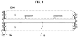
- FIG. 1 is a view for explaining a comparative example for comparison with various embodiments of the present disclosure.
- the flexible circuit board 1000 of the comparative example is cut and used in a form in which the sensing portion of a battery cell is formed to be wide.
- the flexible circuit board 1000 is cut in such a shape as to include a band-shaped central portion 1110, connecting portions 1120 formed at both ends of the central portion 1110 and arranged so as to face each other, and third connection circuit portions 1150 protruding from the connecting portions 1120 so as to be connected to a bus bar.
- a problem may be posed in that the waste portions (a) formed on both sides of the central portion 1110 is increased and the production yield of the flexible circuit board 1000 is reduced to some extent. Furthermore, there may be posed a problem in that in the process of assembling the flexible circuit board 1000 to the frame, the flexible circuit board is broken or torn due to an external force or the like and the electric device mounted on the flexible circuit board is damaged. As a result, a problem may be posed in that cracks are generated in the portions of the flexible circuit board bent as side plates due to the severe vibration or impact applied to the battery module.
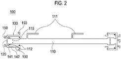
- FIG. 2 is a plan view of a flexible circuit board 100 according to one embodiment of the present disclosure.
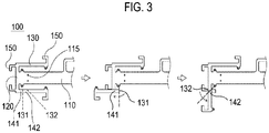
- FIG. 3 is a view showing a folding method of the flexible circuit board 100 shown in FIG. 2 .
- FIG. 4 is a perspective view showing a final shape of a connecting portion on one side of the flexible circuit board 100 shown in FIG. 2 .
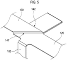
- FIG. 5 is an enlarged perspective view of the overlapped portion 140 shown in FIG. 4 .
- FIG. 6 is a perspective view showing a method in which the first overlapped portion 141 and the second overlapped portion 142 shown in FIG. 5 are fixed by an adhesive 200.
- the flexible circuit board 100 installed on a frame coupled with a bus bar and configured to sense a voltage of a battery cell may include a band-shaped central portion 110, first connection circuit portions 120 formed at both ends of the central portion 110 and disposed to face each other, and second connection circuit portions 130 bent to extend from the first connection circuit portions 120 and formed in parallel with the central portion 110.
- Third connection circuit portions 150 may be formed to extend from the first connection circuit portions 120 and the second connection circuit portions 130 and may be connected to a bus bar.
- each of the second connection circuit portions 130 When each of the second connection circuit portions 130 is folded to one side of each of the first connection circuit portions 120, an overlapped portion 140 may be formed between each of the first connection circuit portions 120 and each of the second connection circuit portions 130. When the overlapped portion 140 is formed, each of the second connection circuit portions 130 may be disposed on the same line as each of the first connection circuit portions 120.
- a substrate layer 101 may be formed at the center of the flexible circuit board 100 in the cross-sectional direction, and insulating layers 102 may be laminated and formed above and below the substrate layer 101.
- the substrate layer 101 may be formed of a circuit for transmitting information as an electrical signal.
- the insulating layers 102 may protect the substrate layer 101 and may prevent the substrate layer 101 from being shortcircuited with other conductive components.
- the substrate layer 101 is formed of an electrically conductive metal layer and may be formed of a copper plate having high electrical conductivity.
- the insulating layers 102 may be made of a non-electrically conductive material in the form of films PEN, Pl. Furthermore, each of the substrate layer 101 and the insulating layers 102 has flexibility and may be easily deformed.
- the flexible circuit board 100 may include the central portion 110, the first connection circuit portions 120 and the second connection circuit portions 130.
- the overlapped portions 140 may be formed between the first connection circuit portions 120 and the second connection circuit portions 130.
- the first connection circuit portions 120, the second connection circuit portions 130 and the overlapped portions 140 may correspond to portions of the flexible circuit board 100 and may be integrally formed with the central portion 110 to constitute one flexible circuit board.
- a first fixing hole 115 may be formed at an end of the central portion 110. Furthermore, protrusion holes 112 may be additionally formed in the portions protruding from the central portion 110 and the second connection circuit portions 130.
- the center portion 110 may be formed to be long in a band shape. Temperature sensing portions 111 may extend outwardly from the central portion 110. The temperature sensing portions 111 may be provided so as to extend to one side. The temperature sensing portions 111 may be configured to measure the temperature of a battery cell and to transmit the measured temperature as electrical information to an external device through the flexible circuit board 100 so that a phenomenon such as overheating or the like can be detected.
- the first connection circuit portions 120 and the second connection circuit portions 130 may be formed at both ends of the center portion 110 in the same form.
- various embodiments of the present disclosure will be described based on the portions formed on one side of the central portion 110.
- the first connection circuit portion 120 is formed at each of both ends of the central portion 110.
- the first connection circuit portion 120 may extend toward both sides from one end of the central portion 110 and may have a shape perpendicular to the central portion 110.
- the first connection circuit portion 120 may extend to the opposite sides across the central portion 110.
- the second connection circuit portions 130 may be bent from the first connection circuit portion 120.
- the second connection circuit portions 130 are bent at a right angle with respect to the first connection circuit portion 120 to extend in parallel with the central portion 110.
- the second connection circuit portions 130 may be formed at each end of the first connection circuit portion 120.
- four second connection circuit portions 130 may be formed in one flexible circuit board 100.
- the overlapped portion 140 may be formed between the first connection circuit portion 120 and the second connection circuit portions 130.
- the overlapped portion 140 may be defined as a portion where the second connection circuit portions 130 is folded to one side of the first connection circuit portion 120 and is overlapped in a plurality of layers.
- the overlapped portion 140 may include a first overlapped portion 141 formed by folding the second connection circuit portion 130 upward toward the first connection circuit portion 120 along a first bending line 131 and a second overlapped portion 142 formed by further folding the second connection circuit portion 130 upward in the longitudinal direction of the first connection circuit portion 120 of the first overlapped portion 141 along a second bending line 132. That is, the overlapped portion 140, which is formed by folding the second connection circuit portion 130 along the first bending line 131 and the second bending line 132, corresponds to a part of the second connection circuit portion 130.
- the second connection circuit portion 130 may be disposed in parallel with the first connection circuit portion 120.
- the third connection circuit portion 150 formed on the second connection circuit portion 130 may be disposed in parallel with the third connection circuit portion 150 formed on the first connection circuit portion 120.
- the case where two components are disposed in parallel includes not only a case where two components are completely parallel to each other so that the extension lines thereof do not meet with each other but also a case where two components are inclined at a predetermined angle so as to be substantially parallel to each other.
- the first bending line 131 may be formed in parallel with the longitudinal direction of the first connection circuit portion 120.
- the second bending line 132 may be formed in an oblique direction so as to make an angle of about 45 degrees with respect to the first bending line 131.
- a folding method of the second connection circuit portion 130 will be described with reference to FIG. 3 .
- first state in which the second connection circuit portion 130 is formed in parallel with the central portion 110, the second connection circuit portion 130 is folded along the first bending line 131 to the upper side of the first connection circuit portion 120 and comes into a state (second state) in which the second connection circuit portion 130 is formed parallel with the central portion 110 on the opposite side of the central portion 110.
- second state in which the second connection circuit portion 130 is formed parallel with the central portion 110 on the opposite side of the central portion 110.
- the first overlapped portion 141 is formed between the first connection circuit portion 120 and the second connection circuit portion 130.
- the second connection circuit portion 130 is fold to the upper side of the first overlapped portion 141 along the second bending line 132 comes into a state (third state) in which the second connection circuit portion 130 is disposed on the same line as the first connection circuit portion 120.
- the second overlapped portion 142 may be formed between the first overlapped portion 141 and the second connection circuit portion 130.
- Two overlapped portions 140 and two bending lines 131 and 132 are not necessarily formed on the basis of one second connection circuit portion 130.
- the number of the overlapped portions 140 and the bending lines 131 and 132 may be differently set depending on the cut shape and final shape of the flexible circuit board 100.
- Portions of the second connection circuit portion 130 that constitute the first overlapped portion 141 and the second overlapped portion 142 may be tightly fixed by an adhesive 200.
- the adhesive 200 may be configured to provide fixing forces on the upper side and the lower side thereof.
- the adhesive 200 may be, for example, a double-sided tape or a double-sided pad. The use of the adhesive 200 makes it possible to minimize the increase in the thickness of the flexible circuit board 100 due to the overlapping of the portions of the flexible circuit board 100 and to prevent lifting of the portions of the flexible circuit board 100, thereby preventing damage due to vibration in an assembling process or during a vehicle transportation.
- the flexible circuit board 100 may have a final shape after the folding operation, which is different from the cut shape before the bending operation. Accordingly, it is possible to improve the yield in the manufacturing process of the flexible circuit board 100 and to sense a voltage of each of the plurality of battery cells stacked in an increased width.
- FIG. 7 is a perspective view showing a state in which the substrate layer of the third connection circuit portion 150 shown in FIG. 4 is exposed.
- FIG. 8 is a plan view showing the first surface 151 and the second surface 152 shown in FIG. 7 .
- FIG. 9 is a sectional view showing a cross section of the third connection circuit portion 150 shown in FIG. 8 .
- the third connection circuit portion 150 is formed to extend from each of the first connection circuit portion 120 and the second connection circuit portion 130 so as to be branched from each of the first connection circuit portion 120 and the second connection circuit portion 130 and may be joined to a bus bar on one side thereof.
- the first connection circuit portion 120 may be formed with a plurality of third connection circuit portions 150 extending in the same direction.
- one third connection circuit portion 150 may be formed at the end of the second connection circuit portion 130.
- the third connection circuit portions 150 may be disposed side by side in the same direction so that, in the state (third state) in which the second connection circuit portion 130 is disposed on the same line as the first connection circuit portion 120, the third connection circuit portion 150 formed in the second connection circuit portion 130 protrude in the same direction as the third connection circuit portions 150 formed in the first connection circuit portion 120.
- the third connection circuit portion 150 may be connected to the bus bar and may measure the voltage and current of each of the battery cells and transmit the voltage and current as electrical information along the substrate layer 101. Accordingly, the number of the third connection circuit portions 150 may be increased or decreased according to the number of battery cells and the number of bus bars.
- the third connection circuit portions 150 may be formed such that the internal substrate layer 101 of the flexible circuit board 100 is exposed on both side surfaces thereof.
- the substrate layer 101 may include a first surface 151 making contact with the bus bar and a second surface 152 formed and exposed on the opposite side of the first surface 151.
- the size of the first surface 151 may be larger than the size of the second surface 152. Such a structure may facilitate joining of the first surface 151 and the bus bar, and may reduce the externally exposed portion of the substrate layer 101 to minimize damage to the substrate layer 101.
- the third connection circuit portion 150 may be formed such that one surface of the internal substrate layer 101 is exposed.
- the opposite surface of the substrate layer 101 may be covered with an insulating layer.
- one exhaust surface of the substrate layer 101 may make contact with the bus bar.
- the bus bar and the third connection circuit portion 150 may be directly joined to each other, thereby reducing the number of work steps and reducing the weight and cost. This will be explained in detail in the battery module description.
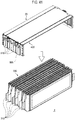
- FIG. 10 is a perspective view of a battery module 1 according to a first embodiment of the present disclosure.
- FIG. 11 is an exploded perspective view of the battery module 1 shown in FIG. 10 .
- FIG. 12 is a perspective view of the cell assembly 300 of the battery module 1 shown in FIG. 10 .
- FIG. 13 is a perspective view of the frame assembly 10 of the battery module 1 shown in FIG. 10 .
- FIG. 14 is a perspective view showing a hinge coupling of the upper plate 410 and the side plate 420 of the frame 400 shown in FIG. 13 .
- the battery module 1 may include a cell assembly 300 formed by stacking one or more battery cells, and a frame assembly 10 for fixing the cell assembly 300.
- the frame assembly 10 may include a frame 400 disposed to surround the cell assembly 300 and provided with an upper plate 410 and side plates 420 connected to both ends of the upper plate 410, bus bars 500 disposed on and fixed to the side plates 420, and a flexible circuit board 100 disposed along the upper plate 410 and the side plates 420 to sense voltages of the battery cells.
- the upper plate 410 may have a path groove 411 recessed at a predetermined depth on the upper surface of the upper plate 410.
- the cell assembly 300 is formed by stacking one or more battery cells.
- the battery cells are usually formed of, but are not limited to, secondary batteries.
- the battery cells may be any rechargeable battery.
- the battery cell protrudes on both sides to form terminal portions 310.
- a (+) terminal is formed on the other side.
- the battery cell is formed of a conductive material and has flexibility so as to be deformable. Accordingly, the terminal portion 310 is folded to one side and electrically connected to the adjacent terminal portion 310 through a joining process.
- the cell assembly 300 may be formed by stacking battery cells in an erected form.
- the terminal portion 310 of the battery cell is connected to the terminal portion 310 of the adjacent battery cell.
- the battery cells are electrically connected in parallel.
- the terminals having different polarities are connected to each other, the battery cells are electrically connected in series.
- connection of the battery cells may be configured differently as needed.
- a 4P/3S connection may be formed by connecting eight battery cells in parallel to form four pairs of battery cells and connecting the four pairs of battery cells in series.
- the battery capacity according to the vehicle package can be easily changed by changing the connection configuration of the battery cells in the cell assembly 300, and the time required for the joining process can be reduced, thereby improving the productivity.
- the frame 400 may include an upper plate 410 and side plates 420 connected to both ends of the upper plate 410.
- the upper plate 410 and the side plates 420 of the frame 400 are hingedly coupled to each other using hook portions 414 formed in the upper plate 410 and rod portions 424 formed in the side plates 420.
- a plurality of hook-shaped hook portions 414 may be formed at the ends of the upper plate 410 in a spaced-apart relationship with each other.
- Rod portions 424 may be formed on the upper surfaces of the side plates 420 in a corresponding relationship with the positions of the hook portions 414.
- the hook portions 414 and the rod portions 424 are formed to protrude from the upper plate 410 and the side plates 420 so as to face each other at one side so that the rod portions 424 can be fitted to and hingedly coupled to the hook portions 414.
- the inner radius of curvature of the hook portion 414 may be equal to or less than the radius of the rod portion 424.
- the frame 400 may be disposed to surround the cell assembly 300 by disposing the upper plate 410 on the upper side of the cell assembly 300 and disposing the side plates 420 on both sides of the cell assembly 300 having the terminal portion 310.
- the upper plate 410 and the side plates 420 may be formed by injection molding a plastic. Accordingly, the frame 400 is low in production cost and can be easily assembled by hinge coupling.
- FIG. 15 is a side view showing the arrangement of the frame 400 of the battery module 1 shown in FIG. 10 and the flexible circuit board 100.
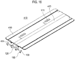
- FIG. 16 is a perspective view showing a combined structure of the upper plate 410 of the frame assembly 10 shown in FIG. 13 and the flexible circuit board 100.
- FIG. 17 is an exploded perspective view showing an exploded configuration of the upper plate 410 shown in FIG. 16 and the flexible circuit board 100.
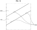
- FIG. 18 is a plan view showing a state in which the flexible circuit board 100 is seated in the path groove 411 of the upper plate 410 shown in FIG. 17 .
- FIG. 19 is a front view of the side plate 420 of the battery module 1 shown in FIG. 10 .
- FIG. 20 is an enlarged perspective view showing the reinforcing plate 600 shown in FIG. 19 .
- FIG. 21 is a sectional perspective view and a sectional view taken along line A-A in FIG. 20 .
- FIG. 22 is a view showing a fixing method of the reinforcing plate 600 shown in FIG. 20 .
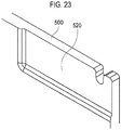
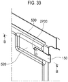
- FIG. 23 is an enlarged perspective view of the seat portion 520 of the bus bar 500 shown in FIG. 19 .
- the flexible circuit board 100 is disposed along the outer side of the frame 400.
- the central portion 110 may be disposed on the upper surface of the upper plate 410.
- the central portion 110 is seated on and fixed to the path groove 411 recessed at a predetermined depth.
- the length of the center portion 110 is larger than the length of the upper plate 410. Both ends of the central portion 110 may be bent along the side plates 420.
- the first connection circuit portion 120 and the second connection circuit portion 130 are disposed on the outer side of the side plate 420 and are bent to make close contact with the outer surface of the side plate 420. Accordingly, the third connection circuit portions 150 formed in the first connection circuit portion 120 and the second connection circuit portion 130 may be structurally disposed outside the bus bar 500.
- protrusion holes 112 may be formed in the central portion 110 and the second connection circuit portion 130.
- the protrusion holes 112 are provided in plural, fastening members (not shown) may be inserted into the protrusion holes 112 to fix the flexible circuit board 100 to the frame 400.
- the protrusion holes 112 are formed so as to protrude outward and, therefore, do not affect the internal circuit.
- One end of the flexible circuit board 100 is electrically connected to the bus bar 500.
- a plurality of wires are arranged in parallel inside the bus bar 500 to transmit information on the voltage and current of the battery cells to a battery management system (BMS) (not shown).
- BMS battery management system
- the BMS manages the charging and discharging of each battery cell. For example, in a charging mode, the BMS may charge a plurality of battery cells discharged at different voltage levels, so as to have a uniform voltage level.
- the upper plate 410 is formed in a rectangular shape corresponding to the size of the cell assembly 300 and is disposed on the upper side of the cell assembly 300.
- a path groove 411 in which the central portion 110 is seated is formed on the upper surface of the upper plate 410.
- the upper plate 410 includes a top cover 413 that covers the upper side of the path groove 411.
- the path groove 411 may be formed to have a predetermined depth so that the central portion 110 can be seated in the path groove 411.
- the top cover 413 may cover the upper side of the central portion 110 in a state in which the central portion 110 is seated in the path groove 411. Therefore, the path groove 411 and the top cover 413 may be formed in the same shape as the shape of the central portion 110. Accordingly, the central portion 110 is prevented from being removed to the outside of the frame 400 and from being exposed to the outside. This makes it possible to avoid damage that may occur in the central portion 110 during the assembly process.
- Ribs 412 protruding toward the inside of the path groove 411 may be formed in the upper plate 410.
- the ribs 412 may be alternately formed on both sides of the path groove 411 and may be spaced apart from each other by a predetermined distance.
- the ribs 412 may be formed to protrude inwardly from both sides of the path groove 411 and the lower surface of the rib 412 may be spaced apart from the path groove 411 at a predetermined interval. Therefore, the central portion 110 is disposed between the ribs 412 and the path groove 411 and is prevented from being removed from the path groove 411.
- the flexible circuit substrate 100 can be closely fixed to the frame 400 without having to use an adhesive such as a double-sided tape or the like.
- the reinforcing plate 600 and the bus bar 500 may be closely fixed to the outer surface of each of the side plates 420.
- Two side plates 420 are connected to both ends of the upper plate 410, respectively.
- the two side plates 420 may be disposed on both side surfaces of the cell assembly 300.
- Both side surfaces of the cell assembly 300 may be both sides where the terminal portions 310 of the battery cells are formed.
- the reinforcing plate 600 may cover the end of the central portion 110 and may be closely fixed to each of the side plates 420.
- Each of the side plates 420 may be provided with fusion protrusions 425 protruding from each of the side plates 420 for fixing the reinforcing plate 600.
- Fixing holes 115 and 615 may be formed in the central portion 110 and the reinforcing plate 600 in a corresponding relationship with the positions of the fusion protrusions 425, respectively.
- the reinforcing plate 600 may be fixed by a fusion method after the fusion protrusions 425 sequentially pass through the first fixing holes 115 of the central portion 110 and the second fixing holes 615 of the reinforcing plate 600.
- a thermal fusion process the fusion protrusions 425 are melted down from the outside and compressed by a pressing member (not shown) provided with a heater. Thereafter, the compressed portions of the fusion protrusions 425 are cooled and hardened so that the reinforcing plate 600 can be brought into close contact with each of the side plates 420.
- the end of the central portion 110 may be disposed and fixed between the reinforcing plate 600 and each of the side plates 420. Since the reinforcing plate 600 moves beyond the bent portion of the central portion 110 and presses the lower end portion of the central portion 110, it is possible to minimize the additional bending of the flexible circuit board 100 by pressurization. This makes it possible to prevent occurrence of damage such as cracks or the like In addition, it is possible to prevent the flexible circuit board 100 from being directly pressed in the thermal fusion process and to absorb external forces such as continuous vibrations or impacts caused by the driving of a vehicle, thereby minimizing damage.
- the fusion process referred to herein may include not only a thermal fusion process but also an ultrasonic fusion process.
- the reinforcing plate 600 may be made of any circuit-less insulating material except for metal so as not to hinder the electrical connection between the flexible circuit board 100 and the bus bar 500.
- the bus bar 500 may be closely fixed to each of the side plates 420. A portion of the bus bar 500 may be connected to the third connection circuit portion 150 and the other portion thereof may be connected to the terminal portion 310. Therefore, the bus bar 500 may be configured to electrically connect the flexible circuit board 100 and the battery cells.
- bus bars 500 may be provided in a spaced-apart relationship with each other.
- the number of the bus bars 500 may be changed as needed.
- insertion holes 510 and seat portions 520 may be formed in each of the bus bars 500.
- the seat portions 520 may be portions of each of the bus bars 500, which are joined to the third connection circuit portions 150 of each of the bus bars 500, and may be formed to have a predetermined depth. Therefore, a worker is capable of visually recognizing a working position based on the seat portions 520 and is capable of clearly grasping a joining position. As a result, it is possible to solve problems such as defective joining and the like.
- the insertion holes 510 may be formed along the same direction as the stacking direction of the battery cells.
- the terminal portions 310 of the cell assembly 300 are inserted into the insertion holes 510.
- the portions of the terminal portions 310 protruding through the insertion holes 510 may be folded to one side and may be joined to each of the bus bars 500. Accordingly, the battery cells may be electrically connected to other battery cells through each of the bus bars 500.
- holes may also be formed in the side plates 420 in a corresponding relationship with the positions where the insertion holes 510 are formed for the insertion of the terminal portions 310.
- the bus bars 500 may include a sensing bus bar and an HV bus bar which are formed independently of each other.
- the bus bars 500 may be electrically connected to the terminal portions 310 of the cell assembly 300 to transmit information on the voltage and current of each battery cell or may be connected to the bus bars provided outside the battery module 1 to transmit electrical information.
- the bus bars 500 may be made of a conductor and may be made of metal having high electrical conductivity.
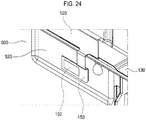
- FIG. 24 is a front view showing a state in which the substrate layer 101 is directly bonded to the seat portion 520 shown in FIG. 23 .
- FIG. 25 is a sectional view showing a bonding method for bonding the substrate layer 101 shown in FIG. 24 to the bus bar 500.
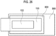
- FIG. 26 is a plan view showing a state in which a coating portion 800 is further formed on the third connection circuit portion 150 shown in FIG. 24 .
- FIG. 27 is a sectional view of the coating layer shown in FIG. 26 .
- the substrate layer 101 may include a first surface 151 configured to make contact with the bus bar 500 and a second surface 152 formed on the opposite side of the first surface 151.
- a coating portion 800 may be further formed on the outer side of the second surface 152.
- the first surface 151 and the second surface 152 may be formed by cutting the insulating layers 102 of the flexible circuit substrate 100 to expose the internal substrate layer 101.
- the first surface 151 may be in contact with one side of the bus bar 500 and may make contact the seat portion 520 recessed at a predetermined depth in the bus bar 500.
- the seat portion 520 clearly indicates the position where the third connection circuit portion 150 is joined. This makes it possible to improve the workability.
- the size of the first surface 151 may be larger than the size of the second surface 152. According to this embodiment, it is possible to secure a welding area over which the substrate layer 101 is welded to the bus bar 500 and to reduce the area of the substrate layer exposed to the outside, thereby preventing the third connection circuit portion 150 from being damaged.
- the substrate layer 101 is configured to serve as a circuit of the flexible circuit board 100 and is made of an electrically conductive material.
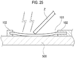
- the substrate layer 101 may electrically connect the bus bar 500 and the flexible circuit board 100 by directly joining the first surface 151 and the seat portion 520. In this process, the first surface 151 may be joined by performing laser welding outside the second surface 152.
- the first surface 151 may be an exposed surface formed by cutting the insulating layer 102. If there is an air gap corresponding to the outside of the seat portion 520 and the thickness of the insulating layer 102, the substrate layer 101 may be blackened in the joining process due to the air gap, or the insulating layers 102 may be burned. Thus, the required quality may not be achieved.
- the air gap existing between the first surface 151 and the seat portion 520 may be removed by pressing the second surface 152 with a jig Z in the joining process.
- the contact area between the seat portion 520 and the first surface 151 is increased by the pressing operation. This makes it possible to enhance the fixing force of the welded portion.
- the third connection circuit portion 150 is configured to be exposed on both sides of the substrate layer 101, the third connection circuit portion 150 may have a structure that can be directly coupled to the bus bar 500. Therefore, it is possible to reduce the number of parts to be used and to reduce the number of work steps, thereby improving the productivity.
- the coating portion 800 may be formed to cover the second surface 152 and a portion of the bus bar 500 around the third connection circuit portion 150.
- the coating portion 800 may be made of a nonconductive material so as not to hinder the electrical connection between the substrate layer 101 and the bus bar 500, and may be applied to only a part of the bus bar 500 using a nozzle.
- the coating portion 800 may be formed in a state in which the first surface 151 is joined to the bus bar 500. Furthermore, the coating portion 800 may be formed to cover a portion of the insulating layer 102 and a portion of the bus bar 500. This makes it possible to prevent corrosion of the substrate layer 101 and to improve the joining strength with the bus bar 500.
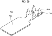
- FIG. 28 is a front view showing a state in which the connecting portion 720 of the integral connection terminal 700 according to one embodiment is joined to the seat portion 520 shown in FIG. 23 .
- FIG. 29 is a perspective view of the integral connection terminal 700 according to one embodiment shown in FIG. 28 .
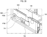
- FIG. 30 is a front view showing a state in which the connecting portion 1720 of a ring-shaped connection terminal 1700 different from the integral connection terminal 700 is joined to the seat portion 520 shown in FIG. 23 .
- FIG. 31 is a perspective view of the ring-shaped connection terminal 1700 shown in FIG. 30 and the fastening member 1730.
- FIG. 32 is a perspective view showing a method in which the fixing portion 710 shown in FIGS. 28 and 30 is fixed to the third connection circuit portion 150.
- the flexible circuit board 100 and the bus bar 500 may be electrically connected by the substrate layer 101 formed in the third connection circuit portion 150 as described in the above embodiment.
- the flexible circuit board 100 and the bus bar 500 may be electrically connected by the connection terminals 700 and 1700 connected to the third connection circuit portion 150 and the bus bar 500.
- the connection terminal 700 or 1700 includes a fixing portion 710 and a connecting portion 720 or 1720.
- the connecting portion 720 or 1720 is integrally formed with the fixing portion 710 to extend from one side of the fixing portion 710.
- the connection terminal 700 or 1700 may be located between the bus bar 500 and the third connection circuit portion 150 and may be connected to the bus bar 500 and the third connection circuit portion 150 to electrically connect them.
- the fixing portion 710 may be fixed to the third connection circuit portion 150 and may be formed to have a relatively small width.
- the fixing portion 710 may be provided with fixing protrusions 711 protruding upward and downward.
- the fixing protrusions 711 are provided so as to be spaced apart from each other and may pass through the third connection circuit portion 150 arranged at a predetermined position. The end portions of the fixing protrusions 711 are bent and fixed to the third connection circuit portion 150.
- connection terminal 700 or 1700 may have various shapes.
- the same reference numerals will be used to denote the same parts even if they correspond to different embodiments.
- the connecting portion 720 of the connection terminal 700 is joined to the seat portion 520 of the bus bar 500 and is formed to have a relatively large width.
- the connecting portion 720 may be joined by laser welding.
- the connecting portion 1720 of the connection terminal 1700 may have a ring shape having a hole 1721 formed at the center thereof.
- the ring-shaped portion may be fixed by a fastening member 1730 such as a screw or the like.
- connection terminal 700 or 1700 unlike the prior art in which a fixing terminal and a connection plate are used to connect a flexible circuit board and a bus bar, the fixing portion 710 and the connecting portion 720 or 1720 are integrally connected to each other. This makes it possible to reduce the number of work steps and to reduce the manufacturing cost, thereby improving the productivity.
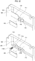
- FIG. 33 is a perspective view showing a state in which a coupling member 2700 is coupled to the seat portion 520 shown in FIG. 23 .
- FIG. 34 is a perspective view showing a coupling method for coupling the coupling member 2700 to the seat portion 520 shown in FIG. 33 .
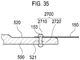
- FIG. 35 is a sectional view taken along line B-B in FIG. 33 .
- the flexible circuit board 100 and the bus bar 500 can be electrically connected to each other by the substrate layer 101 formed in the third connection circuit portion 150 or the connection terminal 700 or 1700 as described above.
- a coupling member 2700 may be doubly joined between the third connection circuit portion 150 and the bus bar 500 to electrically connect the third connection circuit portion 150 and the bus bar 500.
- the coupling member 2700 may include a head 2710 disposed outside the third connection circuit portion 150 and a joint portion 2720 extending from the head 2710.
- the joint portion 2720 may electrically connect the flexible circuit board and the bus bar. Accordingly, the coupling member 2700 is made of metal material having electrical conductivity.
- the head 2710 protrudes outward from the joint portion 2720 to press the third connection circuit portion 150 toward the seat portion 520, thereby fixing the third connection circuit portion to the seat portion 520.
- a first coupling hole 521 may be formed in the seat portion 520 so that the coupling member 2700 can be coupled with the first coupling hole 521, and a second coupling hole 153 may be formed in the third coupling circuit portion 150 in correspondence with the position of the first coupling hole 521.
- a pair of first coupling holes 521 and a pair of second coupling holes 153 may be formed in a spaced-apart relation with each other and formed into a pair and may have the same inner diameter.
- the joint portion 2720 may be fixed to the bus bar 500 through the second coupling hole 153 and the first coupling hole 521 when the coupling member 2700 is coupled.
- the head 2710 is formed to extend outward from the joint portion 2720 and is disposed to protrude outside the third connection circuit portion 150.
- the joint portion 2720 may be formed to have the same size as the first coupling hole 521 and the second coupling hole 153, and the head 2710 may have a radius larger than the radius of the joint portion 2720. Therefore, the head 2710 may be disposed outside the third connection circuit portion 150 without passing through the first coupling hole 521 and the second coupling hole 153.
- the joint portion 2720 of the coupling member 2700 is electrically connected to the substrate layer 101 of the third connection circuit portion 150 through the second coupling hole 153 and is then electrically connected to the bus bar 500 through the first coupling hole 521.
- the coupling member 2700 can electrically connect the flexible circuit board and the bus bar.
- the coupling member 2700 may be composed of a rivet that provides a permanent binding force between thin members.
- a rivet it is possible to fundamentally prevent distortion due to a welding process or occurrence of cracks or the like generated at a welding portion, thereby improving the coupling reliability.
- a battery module 2 according to a second embodiment of the present disclosure is partially identical with the battery module 1 according to the above-described first embodiment. Thus, the duplicate descriptions of the same components will be omitted.
- FIG. 36 is a perspective view of a battery module 2 according to a second embodiment of the present disclosure.
- FIG. 37 is a side view showing an exploded configuration of the frame 400 shown in FIG. 36 and the flexible circuit board 100.
- FIG. 38 is a bottom perspective view of the frame 400 shown in FIG. 36 .
- FIG. 39 is an exploded view of the upper plate 410 shown in FIG. 38 and the flexible circuit board 100.
- the battery module 2 may include a cell assembly 300 formed by stacking one or more battery cells and a frame assembly 20 for fixing the cell assembly 300.
- the frame assembly 20 may include a frame 400 disposed to surround the cell assembly 300 and provided with an upper plate 410 and side plates 420 connected to both ends of the upper plate 410, bus bars 500 disposed on and fixed to the side plates 420, a flexible circuit board 100 disposed along the upper plate 410 and the side plates 420 to sense a voltage of the battery cells, and reinforcing plates 600 closely fixed to one sides of the side plates 420 to cover the ends of the flexible circuit board 100.
- the upper plate 410 may have a protection groove 416 formed at a predetermined depth on the bottom surface of the upper plate 410.
- the central portion 110 of the flexible circuit board 100 may be disposed on the bottom surface of the upper plate 410, and first connection circuit portion 120 and the second connection circuit portion 130 may be disposed on the outer surface of each of the side plates 420.
- the central portion 110 is positioned between the upper plate 410 and the cell assembly 300 so that the portion of the flexible circuit board exposed to the outside of the battery module 2 can be minimized.
- damage to the flexible circuit board 100 such as tearing due to cracks or the like which may occur in an assembly process.
- a protection groove 416 in which the central portion 110 is received may be formed in the upper plate 410 of the frame 400.
- the protection groove 416 may be formed in the same shape as the central portion 110.
- the central portion 110 may be closely fixed to the protection groove 416 by an adhesive 200.
- the adhesive 200 may be a double-sided tape 200 having a shape corresponding to the shape of the central portion 110 and the protection groove 416.
- the thermal fusion process can be minimized during the assembly process of the battery module 2. This makes it possible to shorten the production time and to prevent the breakage of the flexible circuit board 100 which may be generated by a pressing operation in a fusion process.
- a protection hole 417 may be formed in at least one of the upper plate 410 and the side plates 420 in a corresponding relationship with the position where the protection groove 416 is formed. The end of the central portion 110 passes through the protection hole 417 so that the first connection circuit portion 120 and the second connection circuit portion 130 can be disposed on the outer surface of each of the side plates 420.
- the central portion 110 may be bent through the protection hole 417 and may be partially separated.
- the protection hole 417 may be formed in the upper plate 410 in order to minimize such a problem.
- first connection circuit portion 120 and the second connection circuit portion 130 are formed to become wider than the central portion 110. Therefore, if the central portion 110 is accommodated in and fixed to the protection groove 416 before the upper plate 410 and the side plates 420 are hingedly coupled to each other, it is possible to facilitate the assembly of the frame assembly 20.
- FIG. 41 is a perspective view showing a direction in which the frame assembly 20 is assembled to the cell assembly 300.
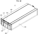
- FIG. 42 is a perspective view showing a state in which the terminal portion 310 is inserted into the insertion hole 510 after the cell assembly 300 and the frame assembly 20 are assembled.
- FIG. 43 is a perspective view showing a state in which the terminal portion 310 is inserted into the insertion hole 510 and is then folded and connected to the bus bar 500.
- FIG. 44 is an enlarged perspective view of the terminal portion 310 shown in FIG. 43 .
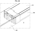
- FIG. 45 is a perspective view showing a method of assembling the battery module 2 and the mono frame 900.
- the terminal portions 310 of one battery cell may be connected to the terminal portions 310 of the adjacent battery cells to form a stacked cell assembly 300. At this time, the terminal portions 310 may be connected to the adjacent terminal portions 310 while protruding from both sides of the battery cells.
- the upper plate 410 and the side plates 420 may be hingedly coupled to each other.
- the flexible circuit board 100 may be disposed along the frame 400 and the third connection circuit portion 150 may be disposed while being joined to the bus bar 500.
- the frame assembly 20 is coupled to the cell assembly 300 from the upper side to the lower side of the cell assembly 300. Since the terminal portions 310 are protruding at this stage, the side plates 420 may be rotated outward about the points of hinge connection with the upper plate 410 so as to spread apart outward with respect to the upper plate 410. Accordingly, the frame assembly 20 may be arranged to surround the outside of the cell assembly 300 without the hindrance of the terminal portions 310.
- the side plates 420 rotated outward may be rotated inward to be positioned at their original positions.
- the protruding terminal portions 310 pass through the holes (not shown) formed in the side plates 420 and the insertion holes 510 formed in the bus bar 500 so that the end portions of the terminal portions 310 can protrude outward of the bus bar 500.
- the end portions of the terminal portions 310 are formed by joining the terminal portions 310 of the battery cell adjacent to each other and are formed by attaching the terminal portions 310.
- the end portions of the terminal portions 310 protruding outward are folded to one side and are joined to the outer surface of the bus bar 500.
- the end portions of the terminal portions 310 do not make contact with the end portions of the adjacent other terminal portions 310. Therefore, the battery cells connected to each other by joining one terminal portion 310 with another terminal portion 310 can be electrically connected to other battery cells only by the bus bar 500.
- the terminal portions 310 and the bus bar 500 can be joined by laser welding at the outer side of the end portions of the terminal portions 310 without providing any separate configuration for coupling. This makes it possible to reduce the time and cost required for the production of the battery module.
- the battery module 2 assembled in the aforementioned manner can be assembled with and fixed to the mono frame 900 once again.
- the mono frame 900 prevents slipping or breakage of the cell assembly 300 when a vehicle suffers from a traffic accident, thereby preventing a secondary accident such as a fire or the like.
- the mono frame 900 protects the joint state of the frame 400 and the cell assembly 300 from an external impact.
- the mono frame 900 may be made of a metallic material having high strength.
Landscapes
- Chemical & Material Sciences (AREA)
- Chemical Kinetics & Catalysis (AREA)
- Electrochemistry (AREA)
- General Chemical & Material Sciences (AREA)
- Engineering & Computer Science (AREA)
- Manufacturing & Machinery (AREA)
- Microelectronics & Electronic Packaging (AREA)
- Connection Of Batteries Or Terminals (AREA)
- Battery Mounting, Suspending (AREA)
Priority Applications (2)
| Application Number | Priority Date | Filing Date | Title |
|---|---|---|---|
| RS20210557A RS61814B1 (sr) | 2016-12-27 | 2017-12-27 | Fleksibilna strujna ploča i okvir koji uključuje istu |
| PL17888917T PL3565022T3 (pl) | 2016-12-27 | 2017-12-27 | Elastyczna płytka obwodu drukowanego i zespół ramy ją zawierający |
Applications Claiming Priority (10)
| Application Number | Priority Date | Filing Date | Title |
|---|---|---|---|
| KR1020160180292A KR101928065B1 (ko) | 2016-12-27 | 2016-12-27 | 버스바 어셈블리의 연결 구조 |
| KR1020160180293A KR101928073B1 (ko) | 2016-12-27 | 2016-12-27 | 버스바 어셈블리의 연결 구조 |
| KR1020160182296A KR101928066B1 (ko) | 2016-12-29 | 2016-12-29 | 버스바 어셈블리의 연결 구조 |
| KR1020160183890A KR101844852B1 (ko) | 2016-12-30 | 2016-12-30 | 배터리셀 모듈의 연성회로기판 고정 구조 |
| KR20170026828 | 2017-02-28 | ||
| KR1020170113677A KR101996449B1 (ko) | 2017-09-06 | 2017-09-06 | 연성회로기판의 보호구조가 구비된 배터리 셀 모듈 |
| KR1020170141527A KR102033001B1 (ko) | 2017-02-28 | 2017-10-27 | 프레임 조립체, 프레임 조립체의 제조 방법 및 배터리 모듈의 제조 방법 |
| KR1020170141526A KR102032999B1 (ko) | 2017-02-28 | 2017-10-27 | 프레임 조립체 및 이를 제조하기 위한 방법 |
| KR1020170159696A KR102087699B1 (ko) | 2017-11-27 | 2017-11-27 | 연성회로기판 및 이를 이용하는 배터리팩 |
| PCT/KR2017/015594 WO2018124751A1 (ko) | 2016-12-27 | 2017-12-27 | 연성회로기판 및 이를 포함하는 프레임 조립체 |
Publications (3)
| Publication Number | Publication Date |
|---|---|
| EP3565022A1 EP3565022A1 (en) | 2019-11-06 |
| EP3565022A4 EP3565022A4 (en) | 2020-03-11 |
| EP3565022B1 true EP3565022B1 (en) | 2021-03-10 |
Family
ID=67483407
Family Applications (1)
| Application Number | Title | Priority Date | Filing Date |
|---|---|---|---|
| EP17888917.6A Active EP3565022B1 (en) | 2016-12-27 | 2017-12-27 | Flexible circuit board and frame assembly including same |
Country Status (7)
| Country | Link |
|---|---|
| US (1) | US11309593B2 (zh) |
| EP (1) | EP3565022B1 (zh) |
| JP (1) | JP6869355B2 (zh) |
| CN (1) | CN110114905B (zh) |
| HU (1) | HUE054599T2 (zh) |
| PL (1) | PL3565022T3 (zh) |
| RS (1) | RS61814B1 (zh) |
Families Citing this family (27)
| Publication number | Priority date | Publication date | Assignee | Title |
|---|---|---|---|---|
| CN112743749A (zh) * | 2017-04-04 | 2021-05-04 | 大山电子株式会社 | 汇流条的制造方法以及通过该制造方法而制造的汇流条 |
| KR102340898B1 (ko) * | 2018-03-30 | 2021-12-16 | 주식회사 엘지에너지솔루션 | 조립성이 향상된 버스바 프레임을 구비한 배터리 모듈 |
| JP6940452B2 (ja) * | 2018-04-18 | 2021-09-29 | 株式会社オートネットワーク技術研究所 | 配線モジュール |
| KR102354401B1 (ko) * | 2018-04-25 | 2022-01-20 | 주식회사 엘지에너지솔루션 | 배터리 모듈 및 이를 포함하는 배터리 팩 |
| JP7081355B2 (ja) * | 2018-07-13 | 2022-06-07 | 株式会社デンソー | 監視装置 |
| CN111448686B (zh) * | 2018-07-26 | 2022-08-12 | 株式会社Lg新能源 | 汇流条组件、电池模块及电池组 |
| KR102395228B1 (ko) | 2018-10-10 | 2022-05-04 | 주식회사 엘지에너지솔루션 | 버스바 프레임 조립 방법 |
| KR102349918B1 (ko) | 2018-11-21 | 2022-01-10 | 주식회사 엘지에너지솔루션 | 배터리 모듈 |
| KR102317638B1 (ko) | 2018-12-05 | 2021-10-25 | 주식회사 엘지에너지솔루션 | 셀 적층체의 보호 구조를 갖는 배터리 모듈 |
| KR102371373B1 (ko) | 2018-12-06 | 2022-03-04 | 주식회사 엘지에너지솔루션 | 전지 모듈 |
| KR102317639B1 (ko) | 2018-12-07 | 2021-10-25 | 주식회사 엘지에너지솔루션 | 인서트 사출된 버스바 조립체를 포함하는 전지 모듈 |
| KR102392767B1 (ko) * | 2018-12-26 | 2022-04-28 | 주식회사 엘지에너지솔루션 | 내측 커버를 포함하는 배터리 모듈 |
| KR102395683B1 (ko) * | 2018-12-26 | 2022-05-06 | 주식회사 엘지에너지솔루션 | Fpcb에 실장된 커넥터를 구비하는 배터리 모듈, 이를 포함하는 배터리 팩 및 자동차 |
| KR102372383B1 (ko) | 2018-12-26 | 2022-03-07 | 주식회사 엘지에너지솔루션 | 에너지 밀도가 향상된 구조를 갖는 배터리 모듈, 이를 포함하는 배터리 팩 및 자동차 |
| KR102423608B1 (ko) | 2019-02-18 | 2022-07-20 | 주식회사 엘지에너지솔루션 | 전지 팩 및 이를 포함하는 디바이스 |
| KR102381762B1 (ko) | 2019-02-21 | 2022-03-31 | 주식회사 엘지에너지솔루션 | 연성 인쇄 회로 기판을 덮는 보호 커버를 포함하는 전지 모듈 |
| JP7016836B2 (ja) * | 2019-06-10 | 2022-02-07 | 矢崎総業株式会社 | 導電システム |
| CN210467965U (zh) * | 2019-09-23 | 2020-05-05 | 宁德时代新能源科技股份有限公司 | 电池模组、电池包以及车辆 |
| CN112582690A (zh) * | 2019-09-29 | 2021-03-30 | 比亚迪股份有限公司 | 柔性电路板、冲切基板和电池装置 |
| KR20210051723A (ko) * | 2019-10-31 | 2021-05-10 | 에스케이이노베이션 주식회사 | 센싱 조립체 및 이를 포함하는 배터리 모듈 |
| CN110993410A (zh) * | 2019-12-20 | 2020-04-10 | 惠州Tcl移动通信有限公司 | 按键模组及终端 |
| JP7177109B2 (ja) * | 2020-03-02 | 2022-11-22 | 矢崎総業株式会社 | 導電モジュール |
| KR20210156089A (ko) * | 2020-06-17 | 2021-12-24 | 주식회사 엘지에너지솔루션 | 버스바와 전압 센싱부재의 연결구조로서 비용접 방식 구조가 적용된 배터리 모듈 |
| KR102485174B1 (ko) * | 2020-08-26 | 2023-01-04 | 한화솔루션 주식회사 | 고단차부 충진이 용이한 배터리 모듈용 버스바 조립체의 제조방법 |
| CN113422151B (zh) * | 2021-06-09 | 2023-02-28 | 东莞新能德科技有限公司 | 电池的制造方法、电池及用电设备 |
| JP7421588B2 (ja) | 2022-03-25 | 2024-01-24 | 本田技研工業株式会社 | バッテリパック |
| CN116706447B (zh) * | 2023-08-04 | 2023-11-24 | 广州凯风新能源科技有限公司 | 一种雾化电源结构及其生产工艺 |
Family Cites Families (48)
| Publication number | Priority date | Publication date | Assignee | Title |
|---|---|---|---|---|
| JP3680720B2 (ja) * | 2000-08-31 | 2005-08-10 | 住友電装株式会社 | 電気接続箱の組み付け方法 |
| JP2002165338A (ja) * | 2000-11-22 | 2002-06-07 | Yazaki Corp | 電気接続箱の回路体配索方法およびその配索方法を用いた回路体配索構造 |
| JP2003204619A (ja) * | 2001-10-24 | 2003-07-18 | Fujikura Ltd | 電気接続箱及びコネクタ |
| US7889139B2 (en) * | 2007-06-21 | 2011-02-15 | Apple Inc. | Handheld electronic device with cable grounding |
| KR100933864B1 (ko) | 2008-03-31 | 2009-12-24 | 삼성에스디아이 주식회사 | 배터리 팩 |
| JP5621765B2 (ja) | 2009-03-31 | 2014-11-12 | 三洋電機株式会社 | 電池モジュール、バッテリシステムおよび電動車両 |
| EP2416436B1 (en) * | 2009-04-01 | 2018-02-21 | LG Chem, Ltd. | Voltage-detecting member, and battery module including same |
| KR101328826B1 (ko) | 2009-11-24 | 2013-11-13 | 엘지디스플레이 주식회사 | 액정표시장치와 그 로컬 디밍 방법 |
| KR101106404B1 (ko) | 2009-11-24 | 2012-01-17 | 삼성에스디아이 주식회사 | 이차 전지 및 그 제조 방법 |
| KR20120005728A (ko) | 2010-07-09 | 2012-01-17 | (주)브이이엔에스 | 서브 팩 모듈 |
| JP2011210710A (ja) | 2010-03-12 | 2011-10-20 | Autonetworks Technologies Ltd | 電池モジュール |
| JP2011210711A (ja) | 2010-03-12 | 2011-10-20 | Autonetworks Technologies Ltd | 電池モジュール |
| US20110255850A1 (en) * | 2010-04-19 | 2011-10-20 | Richard Hung Minh Dinh | Electronic subassemblies for electronic devices |
| JP5715766B2 (ja) | 2010-04-22 | 2015-05-13 | 矢崎総業株式会社 | 配線材の接続構造 |
| US8609266B2 (en) | 2011-02-18 | 2013-12-17 | Samsung Sdi Co., Ltd. | Battery pack |
| KR101273339B1 (ko) | 2011-03-24 | 2013-06-11 | 주식회사 이랜텍 | 적층형 배터리셀 |
| JP2012227004A (ja) | 2011-04-20 | 2012-11-15 | Auto Network Gijutsu Kenkyusho:Kk | 電池接続アセンブリ及び電池モジュール |
| KR101866369B1 (ko) | 2011-07-12 | 2018-06-14 | 에스케이이노베이션 주식회사 | 배터리 케이스 |
| KR101853397B1 (ko) | 2011-09-01 | 2018-04-30 | 엘지전자 주식회사 | 전지모듈 |
| JP2013097894A (ja) * | 2011-10-28 | 2013-05-20 | Auto Network Gijutsu Kenkyusho:Kk | 電池用配線モジュール |
| JP2013098032A (ja) | 2011-11-01 | 2013-05-20 | Auto Network Gijutsu Kenkyusho:Kk | 電圧検知端子の接続構造 |
| US20130149586A1 (en) | 2011-12-09 | 2013-06-13 | Samsung Sdi Co., Ltd. | Battery cell |
| ES2445320T3 (es) * | 2011-12-21 | 2014-03-03 | 3M Innovative Properties Company | Dispositivo de conexión de terminal para un cable eléctrico |
| KR101329250B1 (ko) | 2012-07-06 | 2013-11-13 | 한국단자공업 주식회사 | 배터리모듈용 직렬연결장치의 셀버스바 고정구조 |
| KR101329252B1 (ko) * | 2012-07-11 | 2013-11-13 | 한국단자공업 주식회사 | 배터리모듈용 직렬연결장치 |
| KR101329251B1 (ko) | 2012-07-11 | 2013-11-13 | 한국단자공업 주식회사 | 배터리모듈용 직렬연결장치 |
| US20140193680A1 (en) | 2013-01-08 | 2014-07-10 | Samsung Sdi Co., Ltd. | Battery module |
| KR20140095660A (ko) | 2013-01-24 | 2014-08-04 | 엘지전자 주식회사 | 배터리 셀 케이스 및 이를 포함하는 배터리팩 |
| JP6119385B2 (ja) | 2013-04-03 | 2017-04-26 | 株式会社Gsユアサ | 電池モジュール |
| US20140329124A1 (en) | 2013-05-02 | 2014-11-06 | Arcimoto, Llc | Battery pack design for integrating and monitoring multiple single battery cells |
| KR102046122B1 (ko) | 2013-05-21 | 2019-11-19 | 에스케이이노베이션 주식회사 | Pcb접속유닛 및 이를 이용한 전지모듈제작방법과 상기 방법에 의해 제작된 전지모듈 |
| KR20140139862A (ko) | 2013-05-28 | 2014-12-08 | 삼성에스디아이 주식회사 | 배터리 팩 |
| KR101490026B1 (ko) | 2013-05-31 | 2015-02-06 | 박용미 | 배터리 팩 및 그 생산방법 |
| US20140370355A1 (en) | 2013-06-14 | 2014-12-18 | Samsung Sdi Co., Ltd. | Battery pack |
| KR20150033176A (ko) | 2013-09-23 | 2015-04-01 | 주식회사 엘지화학 | 배터리 모듈 및 이에 적용되는 버스바 |
| KR102258973B1 (ko) | 2013-10-31 | 2021-06-02 | 타이코에이엠피 주식회사 | 센싱 블록 및 이를 포함하는 배터리 패키지 |
| KR20150067694A (ko) | 2013-12-10 | 2015-06-18 | 한국단자공업 주식회사 | 배터리모듈용 연결장치 |
| JP2015118731A (ja) * | 2013-12-16 | 2015-06-25 | 日立金属株式会社 | 配線材、二次電池装置、電子機器、及び配線材の製造方法 |
| KR101723037B1 (ko) | 2014-08-08 | 2017-04-06 | 주식회사 유라코퍼레이션 | 이차전지팩의 이차전지 연결장치 |
| KR20160026469A (ko) | 2014-09-01 | 2016-03-09 | 에스케이이노베이션 주식회사 | 저전압 센싱모듈 일체형 버스바를 구비한 배터리모듈 |
| KR102142661B1 (ko) | 2014-10-07 | 2020-09-14 | 현대자동차주식회사 | 배터리셀 모듈 |
| KR20160044654A (ko) | 2014-10-15 | 2016-04-26 | 세방전지(주) | 전지팩 모듈의 센싱보드 |
| KR102258286B1 (ko) | 2014-10-21 | 2021-05-31 | 에스케이이노베이션 주식회사 | 배터리셀, 및 이를 포함하는 배터리 모듈 |
| KR101750489B1 (ko) | 2014-11-24 | 2017-06-23 | 주식회사 엘지화학 | 전지모듈용 온도 센서 및 이를 포함하는 전지모듈 |
| KR101647694B1 (ko) | 2014-12-15 | 2016-08-23 | 현대오트론 주식회사 | 배터리의 전압을 측정하기 위한 장치 및 그 방법 |
| KR101865995B1 (ko) | 2015-03-27 | 2018-06-08 | 주식회사 엘지화학 | 배터리 모듈 |
| KR20170001135U (ko) | 2015-09-18 | 2017-03-28 | 동우 화인켐 주식회사 | Fpcb 본딩 장치 |
| KR102511737B1 (ko) * | 2018-01-24 | 2023-03-20 | 삼성전자주식회사 | 안테나 구조체 및 안테나 구조체를 포함하는 전자 장치 |
-
2017
- 2017-12-27 PL PL17888917T patent/PL3565022T3/pl unknown
- 2017-12-27 EP EP17888917.6A patent/EP3565022B1/en active Active
- 2017-12-27 RS RS20210557A patent/RS61814B1/sr unknown
- 2017-12-27 CN CN201780081162.4A patent/CN110114905B/zh active Active
- 2017-12-27 US US16/474,414 patent/US11309593B2/en active Active
- 2017-12-27 JP JP2019536176A patent/JP6869355B2/ja active Active
- 2017-12-27 HU HUE17888917A patent/HUE054599T2/hu unknown
Non-Patent Citations (1)
| Title |
|---|
| None * |
Also Published As
| Publication number | Publication date |
|---|---|
| CN110114905A (zh) | 2019-08-09 |
| RS61814B1 (sr) | 2021-06-30 |
| JP6869355B2 (ja) | 2021-05-12 |
| PL3565022T3 (pl) | 2021-10-04 |
| US11309593B2 (en) | 2022-04-19 |
| US20190348720A1 (en) | 2019-11-14 |
| CN110114905B (zh) | 2022-06-24 |
| JP2020514976A (ja) | 2020-05-21 |
| HUE054599T2 (hu) | 2021-09-28 |
| EP3565022A4 (en) | 2020-03-11 |
| EP3565022A1 (en) | 2019-11-06 |
Similar Documents
| Publication | Publication Date | Title |
|---|---|---|
| EP3565022B1 (en) | Flexible circuit board and frame assembly including same | |
| KR102087699B1 (ko) | 연성회로기판 및 이를 이용하는 배터리팩 | |
| EP1992026B1 (en) | Battery module | |
| EP2025019B1 (en) | Middle or large-sized battery module | |
| US9620826B2 (en) | Middle or large-sized battery module | |
| EP2535962B1 (en) | Battery module having enhanced welding reliability and medium or large battery pack including same | |
| JP5584820B2 (ja) | 新規構造を備えた検知部材を有する電池モジュール | |
| CN101395737B (zh) | 中型或大型电池模块 | |
| EP2988344B1 (en) | Battery module having novel structure and battery pack comprising same | |
| KR101305224B1 (ko) | 전지모듈 및 이를 포함하는 전지팩 | |
| EP2416437B1 (en) | Medium or large sized battery module having improved safety | |
| KR20070112490A (ko) | 전지모듈 | |
| KR20130139472A (ko) | 단일 전극단자 결합부를 가진 전지 조합체 | |
| EP3101714B1 (en) | Battery module having voltage sensing member having receptacle structure | |
| EP2662922B1 (en) | Battery pack provided with stable measurement means | |
| KR101136807B1 (ko) | 중대형 전지모듈용 카트리지 |
Legal Events
| Date | Code | Title | Description |
|---|---|---|---|
| STAA | Information on the status of an ep patent application or granted ep patent |
Free format text: STATUS: THE INTERNATIONAL PUBLICATION HAS BEEN MADE |
|
| PUAI | Public reference made under article 153(3) epc to a published international application that has entered the european phase |
Free format text: ORIGINAL CODE: 0009012 |
|
| STAA | Information on the status of an ep patent application or granted ep patent |
Free format text: STATUS: REQUEST FOR EXAMINATION WAS MADE |
|
| 17P | Request for examination filed |
Effective date: 20190729 |
|
| AK | Designated contracting states |
Kind code of ref document: A1 Designated state(s): AL AT BE BG CH CY CZ DE DK EE ES FI FR GB GR HR HU IE IS IT LI LT LU LV MC MK MT NL NO PL PT RO RS SE SI SK SM TR |
|
| AX | Request for extension of the european patent |
Extension state: BA ME |
|
| A4 | Supplementary search report drawn up and despatched |
Effective date: 20200206 |
|
| RIC1 | Information provided on ipc code assigned before grant |
Ipc: H01M 2/20 20060101ALI20200131BHEP Ipc: H01M 10/42 20060101ALI20200131BHEP Ipc: H01M 10/48 20060101ALI20200131BHEP Ipc: H01M 2/34 20060101ALI20200131BHEP Ipc: H01M 2/10 20060101AFI20200131BHEP |
|
| DAV | Request for validation of the european patent (deleted) | ||
| DAX | Request for extension of the european patent (deleted) | ||
| GRAP | Despatch of communication of intention to grant a patent |
Free format text: ORIGINAL CODE: EPIDOSNIGR1 |
|
| STAA | Information on the status of an ep patent application or granted ep patent |
Free format text: STATUS: GRANT OF PATENT IS INTENDED |
|
| INTG | Intention to grant announced |
Effective date: 20201012 |
|
| GRAS | Grant fee paid |
Free format text: ORIGINAL CODE: EPIDOSNIGR3 |
|
| STAA | Information on the status of an ep patent application or granted ep patent |
Free format text: STATUS: GRANT OF PATENT IS INTENDED |
|
| GRAA | (expected) grant |
Free format text: ORIGINAL CODE: 0009210 |
|
| STAA | Information on the status of an ep patent application or granted ep patent |
Free format text: STATUS: THE PATENT HAS BEEN GRANTED |
|
| AK | Designated contracting states |
Kind code of ref document: B1 Designated state(s): AL AT BE BG CH CY CZ DE DK EE ES FI FR GB GR HR HU IE IS IT LI LT LU LV MC MK MT NL NO PL PT RO RS SE SI SK SM TR |
|
| REG | Reference to a national code |
Ref country code: GB Ref legal event code: FG4D |
|
| REG | Reference to a national code |
Ref country code: AT Ref legal event code: REF Ref document number: 1370799 Country of ref document: AT Kind code of ref document: T Effective date: 20210315 Ref country code: CH Ref legal event code: EP |
|
| REG | Reference to a national code |
Ref country code: IE Ref legal event code: FG4D |
|
| REG | Reference to a national code |
Ref country code: DE Ref legal event code: R096 Ref document number: 602017034563 Country of ref document: DE |
|
| REG | Reference to a national code |
Ref country code: LT Ref legal event code: MG9D |
|
| PG25 | Lapsed in a contracting state [announced via postgrant information from national office to epo] |
Ref country code: BG Free format text: LAPSE BECAUSE OF FAILURE TO SUBMIT A TRANSLATION OF THE DESCRIPTION OR TO PAY THE FEE WITHIN THE PRESCRIBED TIME-LIMIT Effective date: 20210610 Ref country code: LT Free format text: LAPSE BECAUSE OF FAILURE TO SUBMIT A TRANSLATION OF THE DESCRIPTION OR TO PAY THE FEE WITHIN THE PRESCRIBED TIME-LIMIT Effective date: 20210310 Ref country code: GR Free format text: LAPSE BECAUSE OF FAILURE TO SUBMIT A TRANSLATION OF THE DESCRIPTION OR TO PAY THE FEE WITHIN THE PRESCRIBED TIME-LIMIT Effective date: 20210611 Ref country code: FI Free format text: LAPSE BECAUSE OF FAILURE TO SUBMIT A TRANSLATION OF THE DESCRIPTION OR TO PAY THE FEE WITHIN THE PRESCRIBED TIME-LIMIT Effective date: 20210310 Ref country code: HR Free format text: LAPSE BECAUSE OF FAILURE TO SUBMIT A TRANSLATION OF THE DESCRIPTION OR TO PAY THE FEE WITHIN THE PRESCRIBED TIME-LIMIT Effective date: 20210310 Ref country code: NO Free format text: LAPSE BECAUSE OF FAILURE TO SUBMIT A TRANSLATION OF THE DESCRIPTION OR TO PAY THE FEE WITHIN THE PRESCRIBED TIME-LIMIT Effective date: 20210610 |
|
| REG | Reference to a national code |
Ref country code: AT Ref legal event code: MK05 Ref document number: 1370799 Country of ref document: AT Kind code of ref document: T Effective date: 20210310 |
|
| REG | Reference to a national code |
Ref country code: NL Ref legal event code: MP Effective date: 20210310 |
|
| PG25 | Lapsed in a contracting state [announced via postgrant information from national office to epo] |
Ref country code: LV Free format text: LAPSE BECAUSE OF FAILURE TO SUBMIT A TRANSLATION OF THE DESCRIPTION OR TO PAY THE FEE WITHIN THE PRESCRIBED TIME-LIMIT Effective date: 20210310 Ref country code: SE Free format text: LAPSE BECAUSE OF FAILURE TO SUBMIT A TRANSLATION OF THE DESCRIPTION OR TO PAY THE FEE WITHIN THE PRESCRIBED TIME-LIMIT Effective date: 20210310 |
|
| REG | Reference to a national code |
Ref country code: HU Ref legal event code: AG4A Ref document number: E054599 Country of ref document: HU |
|
| PG25 | Lapsed in a contracting state [announced via postgrant information from national office to epo] |
Ref country code: NL Free format text: LAPSE BECAUSE OF FAILURE TO SUBMIT A TRANSLATION OF THE DESCRIPTION OR TO PAY THE FEE WITHIN THE PRESCRIBED TIME-LIMIT Effective date: 20210310 |
|
| PG25 | Lapsed in a contracting state [announced via postgrant information from national office to epo] |
Ref country code: AT Free format text: LAPSE BECAUSE OF FAILURE TO SUBMIT A TRANSLATION OF THE DESCRIPTION OR TO PAY THE FEE WITHIN THE PRESCRIBED TIME-LIMIT Effective date: 20210310 Ref country code: SM Free format text: LAPSE BECAUSE OF FAILURE TO SUBMIT A TRANSLATION OF THE DESCRIPTION OR TO PAY THE FEE WITHIN THE PRESCRIBED TIME-LIMIT Effective date: 20210310 Ref country code: EE Free format text: LAPSE BECAUSE OF FAILURE TO SUBMIT A TRANSLATION OF THE DESCRIPTION OR TO PAY THE FEE WITHIN THE PRESCRIBED TIME-LIMIT Effective date: 20210310 Ref country code: CZ Free format text: LAPSE BECAUSE OF FAILURE TO SUBMIT A TRANSLATION OF THE DESCRIPTION OR TO PAY THE FEE WITHIN THE PRESCRIBED TIME-LIMIT Effective date: 20210310 |
|
| PG25 | Lapsed in a contracting state [announced via postgrant information from national office to epo] |
Ref country code: IS Free format text: LAPSE BECAUSE OF FAILURE TO SUBMIT A TRANSLATION OF THE DESCRIPTION OR TO PAY THE FEE WITHIN THE PRESCRIBED TIME-LIMIT Effective date: 20210710 Ref country code: PT Free format text: LAPSE BECAUSE OF FAILURE TO SUBMIT A TRANSLATION OF THE DESCRIPTION OR TO PAY THE FEE WITHIN THE PRESCRIBED TIME-LIMIT Effective date: 20210712 Ref country code: RO Free format text: LAPSE BECAUSE OF FAILURE TO SUBMIT A TRANSLATION OF THE DESCRIPTION OR TO PAY THE FEE WITHIN THE PRESCRIBED TIME-LIMIT Effective date: 20210310 Ref country code: SK Free format text: LAPSE BECAUSE OF FAILURE TO SUBMIT A TRANSLATION OF THE DESCRIPTION OR TO PAY THE FEE WITHIN THE PRESCRIBED TIME-LIMIT Effective date: 20210310 |
|
| REG | Reference to a national code |
Ref country code: DE Ref legal event code: R097 Ref document number: 602017034563 Country of ref document: DE |
|
| PLBE | No opposition filed within time limit |
Free format text: ORIGINAL CODE: 0009261 |
|
| STAA | Information on the status of an ep patent application or granted ep patent |
Free format text: STATUS: NO OPPOSITION FILED WITHIN TIME LIMIT |
|
| PG25 | Lapsed in a contracting state [announced via postgrant information from national office to epo] |
Ref country code: ES Free format text: LAPSE BECAUSE OF FAILURE TO SUBMIT A TRANSLATION OF THE DESCRIPTION OR TO PAY THE FEE WITHIN THE PRESCRIBED TIME-LIMIT Effective date: 20210310 Ref country code: DK Free format text: LAPSE BECAUSE OF FAILURE TO SUBMIT A TRANSLATION OF THE DESCRIPTION OR TO PAY THE FEE WITHIN THE PRESCRIBED TIME-LIMIT Effective date: 20210310 Ref country code: AL Free format text: LAPSE BECAUSE OF FAILURE TO SUBMIT A TRANSLATION OF THE DESCRIPTION OR TO PAY THE FEE WITHIN THE PRESCRIBED TIME-LIMIT Effective date: 20210310 |
|
| 26N | No opposition filed |
Effective date: 20211213 |
|
| PG25 | Lapsed in a contracting state [announced via postgrant information from national office to epo] |
Ref country code: SI Free format text: LAPSE BECAUSE OF FAILURE TO SUBMIT A TRANSLATION OF THE DESCRIPTION OR TO PAY THE FEE WITHIN THE PRESCRIBED TIME-LIMIT Effective date: 20210310 |
|
| PG25 | Lapsed in a contracting state [announced via postgrant information from national office to epo] |
Ref country code: IT Free format text: LAPSE BECAUSE OF FAILURE TO SUBMIT A TRANSLATION OF THE DESCRIPTION OR TO PAY THE FEE WITHIN THE PRESCRIBED TIME-LIMIT Effective date: 20210310 |
|
| PG25 | Lapsed in a contracting state [announced via postgrant information from national office to epo] |
Ref country code: IS Free format text: LAPSE BECAUSE OF FAILURE TO SUBMIT A TRANSLATION OF THE DESCRIPTION OR TO PAY THE FEE WITHIN THE PRESCRIBED TIME-LIMIT Effective date: 20210710 |
|
| PG25 | Lapsed in a contracting state [announced via postgrant information from national office to epo] |
Ref country code: MC Free format text: LAPSE BECAUSE OF FAILURE TO SUBMIT A TRANSLATION OF THE DESCRIPTION OR TO PAY THE FEE WITHIN THE PRESCRIBED TIME-LIMIT Effective date: 20210310 |
|
| REG | Reference to a national code |
Ref country code: CH Ref legal event code: PL |
|
| REG | Reference to a national code |
Ref country code: BE Ref legal event code: MM Effective date: 20211231 |
|
| PG25 | Lapsed in a contracting state [announced via postgrant information from national office to epo] |
Ref country code: LU Free format text: LAPSE BECAUSE OF NON-PAYMENT OF DUE FEES Effective date: 20211227 Ref country code: IE Free format text: LAPSE BECAUSE OF NON-PAYMENT OF DUE FEES Effective date: 20211227 |
|
| PG25 | Lapsed in a contracting state [announced via postgrant information from national office to epo] |
Ref country code: BE Free format text: LAPSE BECAUSE OF NON-PAYMENT OF DUE FEES Effective date: 20211231 |
|
| PG25 | Lapsed in a contracting state [announced via postgrant information from national office to epo] |
Ref country code: LI Free format text: LAPSE BECAUSE OF NON-PAYMENT OF DUE FEES Effective date: 20211231 Ref country code: CH Free format text: LAPSE BECAUSE OF NON-PAYMENT OF DUE FEES Effective date: 20211231 |
|
| PG25 | Lapsed in a contracting state [announced via postgrant information from national office to epo] |
Ref country code: CY Free format text: LAPSE BECAUSE OF FAILURE TO SUBMIT A TRANSLATION OF THE DESCRIPTION OR TO PAY THE FEE WITHIN THE PRESCRIBED TIME-LIMIT Effective date: 20210310 |
|
| P01 | Opt-out of the competence of the unified patent court (upc) registered |
Effective date: 20230821 |
|
| PGFP | Annual fee paid to national office [announced via postgrant information from national office to epo] |
Ref country code: GB Payment date: 20231220 Year of fee payment: 7 |
|
| PGFP | Annual fee paid to national office [announced via postgrant information from national office to epo] |
Ref country code: RS Payment date: 20231214 Year of fee payment: 7 Ref country code: HU Payment date: 20231222 Year of fee payment: 7 Ref country code: FR Payment date: 20231128 Year of fee payment: 7 Ref country code: DE Payment date: 20231214 Year of fee payment: 7 |
|
| PGFP | Annual fee paid to national office [announced via postgrant information from national office to epo] |
Ref country code: PL Payment date: 20231214 Year of fee payment: 7 |
|
| PG25 | Lapsed in a contracting state [announced via postgrant information from national office to epo] |
Ref country code: MK Free format text: LAPSE BECAUSE OF FAILURE TO SUBMIT A TRANSLATION OF THE DESCRIPTION OR TO PAY THE FEE WITHIN THE PRESCRIBED TIME-LIMIT Effective date: 20210310 |